

Samsung S5L9250B01-Q0R0 Datasheet

DATA SHEET S5L9250B
INTRODUCTION
The CD-ROM 48X 1 chip receives the input signal read from the CD-DA/VIDEO-CD/CD-ROM disc after handling
by the RF amplifier. The signal is input into the digital servo block which has a built-in DSP core, and goes
through focus and tracking adjustments. The RF signal input into a data path goes through the data slicer, PLL,
EFM demodulator, C1/C2 ECC and the audio handling block. In the case of a CD-DA, the signal is output through
the 1-bit DAC. In the case of a CD-ROM, the signal is input into an external CD-ROM controller for handling, then
transmitted to the host through the ATAPI I/F. Also, if you operate the CD-DA in audio buffering mode while
already in CAV mode, the signal is stored in the CD-ROM controller DRAM at high speed, then output at 1x from
the CD-ROM controller, after passing through the 1-bit DAC built-in to the S5L9250B.
FEATURES
• Main Features
Digital servo, CD-DSP, 1-bit DAC.
33.8688MHz crystal.
Supports CLV 4X and 8X.
Supports CAV MAX 16X, 20X, 24X, 32X, 40X, and 48X.
Interrupt (SINTB)
MICOM interface
• Digital Servo Block
Automatic adjusting feature (focus/tracking loop offset, balance, loop gain)
Built-in AGC feature that adapts to work optimally with various disc types
Built-in search algorithm for speed control
Servo monitor signal generation (FOK, MIRROR, TZC, ANTI-SHOCK)
Various loop filter coefficient selection by MICOM
Built-in algorithm for handling defects/shocks
Disc discriminating data out (FEpk, SBADpk)
RF IC and serial interface
Built-in 10-bit DAC (Focus/Tracking/SLD)
OAK DSP core
• CD Digital Signal Processing Block
Wide capture range analog PLL
Data Slicer using duty feedback method
EFM demodulation
Sync detection, protection, insertion
CLV, CAV disc spindle motor control
C1/C2 ECC
Built-in 16 K SRAM for ECC
Subcode P - W handling feature
CD-DA Audio handling feature
SUB-Q De-interleaving & CRC check
High speed data transmission support by CD-ROM decoder block for audio buffering (sync mode
selection between subcode sync and CD-DA data)
Digital audio out block
Subcode sync. Insertion, Protection
1

S5L9250B DATA SHEET
• 1-Bit DAC
16-bit ∑ ∆ digital-to-analog converter
On-chip analog postfilter
Filtered line-level outputs, linear phase filtering
90dB SNR
Sampling rate: 44.1kHz
Input rate 1Fs or 2Fs by normal mode/ double mode selection
Digital volume control by MICOM interface
On-chip voltage reference
Digital de-emphasis on/off, digital attenuation
Low clock jitter sensitivity
• Technology & Gate Density
0.35um mixed mode CMOS technology
3.3V power supply (internal core & analog)
5.0V power supply (digital I/O)
Current used: 300mA
Package: 128QFP.
Core used: OAK DSP; ADC for servo use; DAC, 1-bit DAC; 16K SRAM.
Clock used:
1) 33.8688MHz & PLL clock (4.3218MHz * speed coeff.) → DP part.
2) 33.8688MHz or 40MHz synthesized frequency → servo part.
3) 16.9344MHz → 1-bit DAC part.
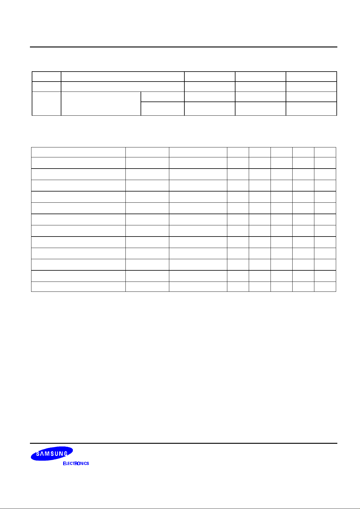
ORDERING INFORMATION
Device Package Operating Temperature
S5L9250B01-Q0R0 128-QFP-1420C -20°C - +75°C
2
DATA SHEET S5L9250B
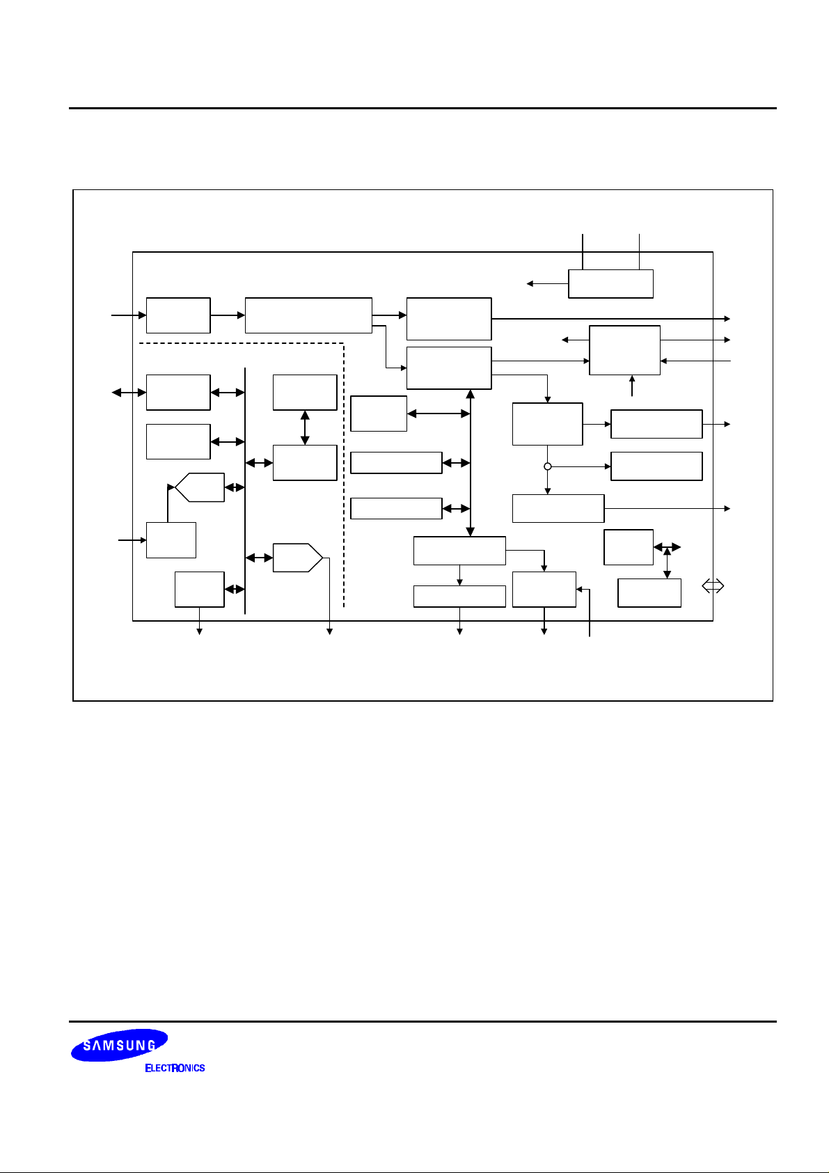
CD-ROM 48X 1 CHIP (DSP+SERVO+1-BIT DAC) BLOCK DIAGRAM
XI XO
33.8688MHz
Timing
RF
Signal
I/O
Signal
Various
Error
Signals
From RF
Data
Slicer
Servo Part
Glue
Logic
Data RAM
512 * 16*2
Analog
Block
10-bit
ADC
PWM
Block
TPWM 1
(bit clock regenerator)
PLL
ROM 8K
Word
OAK Core
10-bit
DAC*4
FOD
Sled 0
TRD
Sled 1
Memory
Control
SRAM for ECC
C1/C2 ECC
CD-DSP Part
EQ Control
Voltage
Generator
EFM
Demodulator
Sync Detector
Audio Processing
Block
DSP I/F
To Servo
Subcode
Processing
Block
Subcode I/F
D/Filter &
1-bit DAC
Analog
Audio
Generator
Spindle
Control
Sub-Q Handling
PSC
CMD
From Servo
D/Audio Out
Block
Micom
I/F
nX-to-1X
CD-DA
Signal
EQ CTL
To Motor
FG
Digital
Audio
Subcode
I/F
Micom
I/F
3
S5L9250B DATA SHEET
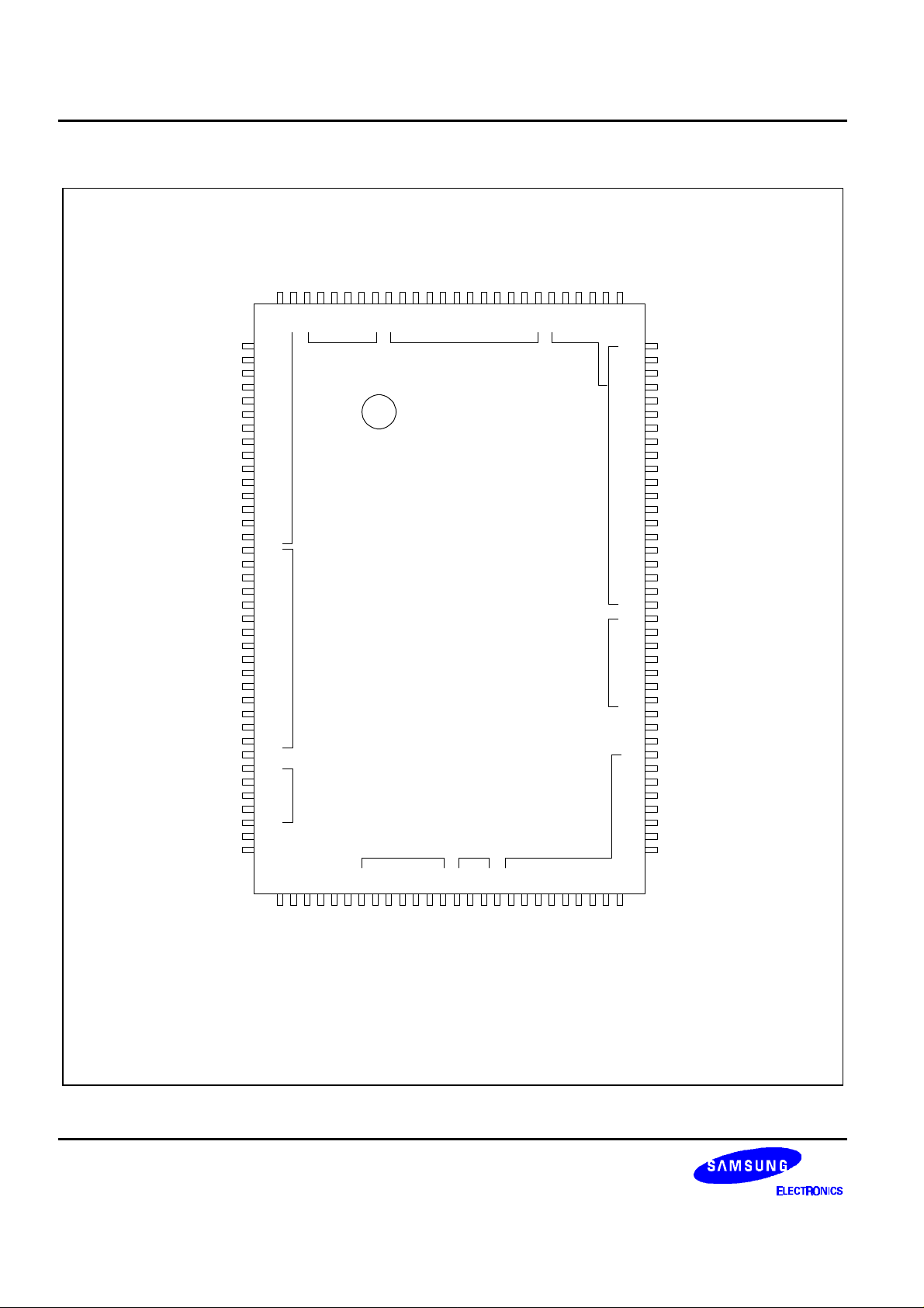
PIN CONFIGURATION
EQCTL
VCCA1(VCCA)
RFI
LPF0
LPF1
VCCA7(VCCA)
EFMCOMP
VSSA7(VSSA)
RISS
VALGC
VCCA6(VSSA)
RVCO
RDAC
VSSA6(VSSA)
VCTRL
VCCA5(VCCA)
VBG
PWMI
PWMO
VSSA5(VSSA)
VHALF
VREF
VCCA4(VCCA)
AOUTR
AOUTL
VSSA4(VSSA)
128
127
126
125
124
123
122
121
120
119
118
117
116
115
114
113
112
111
110
109
108
107
106
105
104
103
102
VSSA1-VSSA
VREFI
VSSA2-VSSA
RFRP
RFCT
SBAD
CEI
TZCA
TE
TELPF
FE
FELPF
VCCA2-VCCA
AOUT
PPUMP
VSSA3-VSSA
TRD
FOD
SLED0
SLED1
SPINDLE
VREFO
VCCA3-VCCA
SMON
DVSS1-VSSOP
GPIO0
SSTOP/GPIO1
PS1/GPIO2
FG
DIRROT
DVDD2-VDD3I
RFEN
RFDATA
RFCLK
DVSS2-VSSI
DFCTI
TEST1
DVDD1-VDD5OP
1
2
3
4
5
6
7
8
9
10
11
12
13
14
15
16
17
18
19
20
21
22
23
24
25
26
27
28
29
30
31
32
33
34
35
36
37
38
Data Slicer
Part
From RF
RF Interface
Motor IFRF IF
PLL Part
KS9250
S5L9050B
EVT3
EVT3
PIN DIAGRAM
PIN DIAGRAM
Micom IF X'tal
i-Bit
DAC
Part
Monitor Part CD-ROM Decoder IF
Micom
IF
101
100
99
98
97
96
95
94
93
92
91
90
89
88
87
86
85
84
83
82
81
80
79
78
77
76
75
74
73
72
71
70
69
68
67
66
65
LRCKI
SDATAI
VDDD1-VDD3I
BCKI
VSSD1-VSSI
SCORO
DVSS12-VSSOP
CK50M
DVDD11-VDD3I
WFCKO
SBSO
DBDD11-VDD5OP
EXCK
DAOUT
DVSS11-VSSOP
BCKO
C2PO
DVSS10-VSSI
LRCKO
SDATAO
GFS
EFML/SL
DVSS9-VSSOP
CLVLOCK
PLCK/EMPH
PLOCK
DVDD8-VDD3I
SCANEN
DVSS8-VSSI
AD0
AD1
AD2
AD3
AD4
AD5
AD6
DVDD7-VDD5OP
AD7
39404142434445464748495051525354555657585960616263
XI
CKO
TEST2
TEST3
TEST4
MIRR/GPIO5
TZCO/GPIO4
TPWM1/GPIO3
NOTES:
1. P1 - P23: Analog
2. P24 - P102: Digital
3. P103 - P128: Digital
DVDD2A(VDD3I)
PHOLD/GPIO6
FOKB/GPIO8
COUT/GPIO7
DVSS4(VSSI)
XO
SENSE
DVSS5(VSSOP)
DVDD3(VDD5OP)
ZRST
SINTB
RDB/DSB
WRB/RWB
DVDD4(VDD3I)
64
CSB
ALE/RSB
DVSS6(VSSI)
DVSS7(VSSOP)
4
DATA SHEET S5L9250B
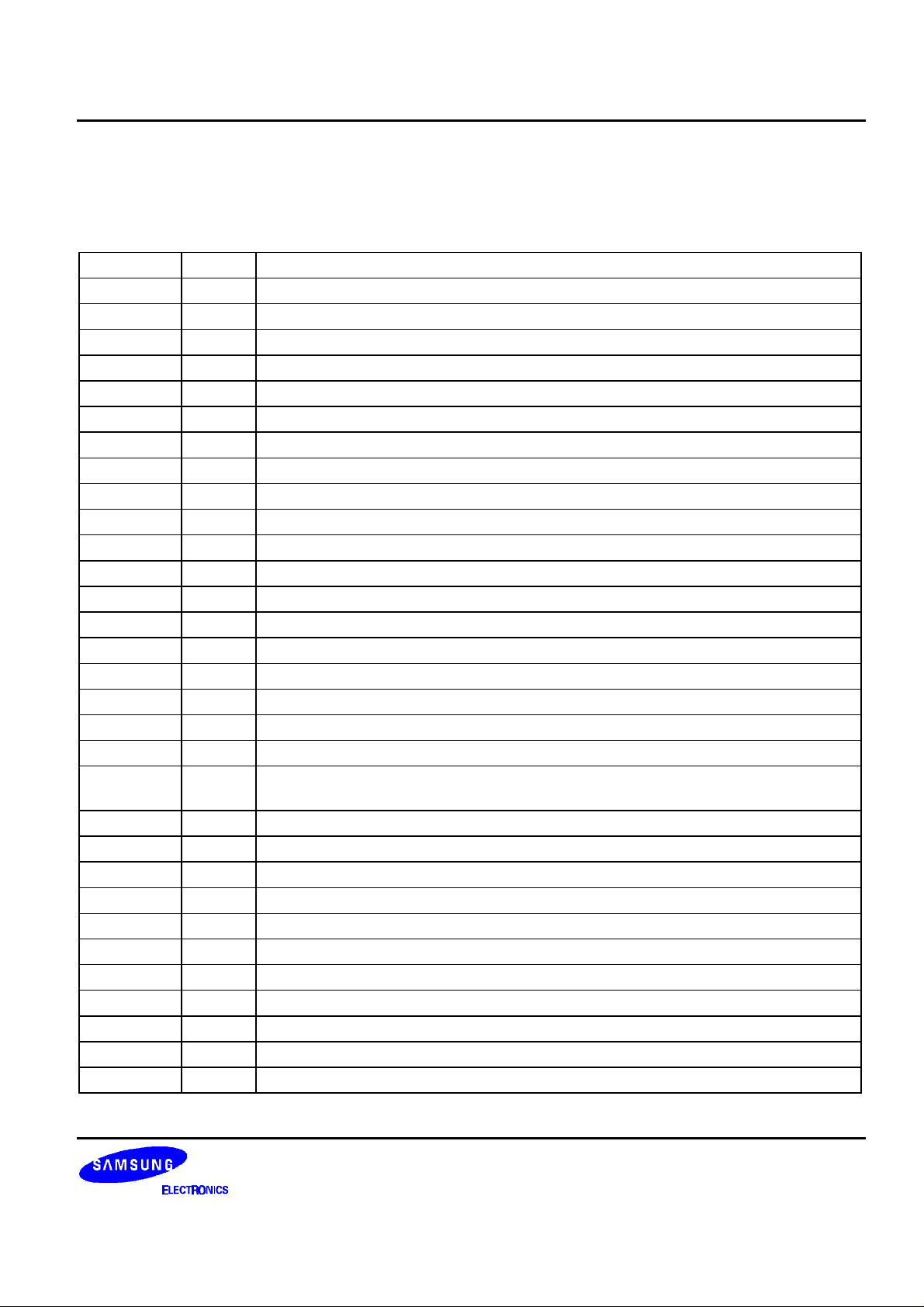
PIN DESCRIPTION
Table 1. Pin Description
No Name Description Related
Block
1 VSSA1 Analog ground (EQ controller) - P VSSA 2 VREFI VREF input SERVO I PICA RF
3 VSSA2 Analog ground (for servo ADC use) - P VSSA 4 RFRP RF envelope signal SERVO I PICA RF
5 RFCT RF envelope's center detection signal SERVO I PICA RF
6 SBAD FOK, DFCT generating SUB-BEAM ADD
signal (E+F)
7 CEI ERROR signal for center servo use SERVO I PICA RF
8 TZCA TZC signal generating signal (=TE) SERVO I PICA RF
9 TE Tracking error signal SERVO I PICA RF
10 TELPF TE defect holding pin SERVO I PICA 11 FE Focusing error signal SERVO I PICA RF
12 FELPF FE defect holding pin SERVO I PICA 13 VCCA2 Analog 3.3V power (for servo ADC use) - P VCCA 14 AOUT Analog out SERVO O POBA MONI
15 PPUMP Pump out for PLL use (filter) SERVO O POBA 16 VSSA3 Analog ground (for servo DAC use) - P VSSA 17 TRD Tracking drive signal (10-bit DAC) SERVO O POBA DRV
18 FOD Focusing drive signal (10-bit DAC) SERVO O POBA DRV
19 SLED0 Stepping control signal 0/DC motor
control signal
20 SLED1 Stepping control signal 1 SERVO O POBA DRV
21 SPINDLE Spindle controlling PWM output CLV O POBA 22 VREFO VREF out for driver IC SERVO O POBA SLED
23 VCCA3 Analog 3.3V power (for DAC use) - P VCCA 24 SMON Spindle motor on/off CLV O PHOB4 MOTOR
25 DVSS1 Digital GND
(for output PAD + PRE driver)
26 GPIO0 General purpose I/O 0 B PHBCT4
27 STOP/GPIO LIMIT switch/sled position sensor
PS0/general purpose I/O
28 PS1/GPIO Sled position sensor signal 1/general
purpose I/O
29 FG Frequency generator signal (for CAV) CLV I PHIC MOTOR
SERVO I PICA RF
SERVO O POBA DRV
- P VSSOP -
SERVO B PHBCT4 -
SERVO B PHBCT4 -
I/O Pad Type To/From
5
S5L9250B DATA SHEET
Table 1. Pin Description (Continued)
No Name Description Related
I/O Pad Type To/From
Block
30 DIRROT Spindle disc rotation direction CLV I PHIC MOTOR
31 DVDD2 Digital 3.3 V power (for internal logic
- P VDD3I -
use)
32 RFEN RF data enable SERVO O PHOB4 RF
33 RFDATA RF serial data SERVO O PHOB4 RF
34 RFCLK RF Interface clock SERVO O PHOB4 RF
35 DVSS2 Digital ground (for internal logic use) - P VSSI 36 DFCTI Defect detection signal SERVO I PHIS RF
37 TEST1 Test mode select TEST I PHICD50 38 DVDD1 Digital 5.0V power
- P VDD5OP -
(for output PAD + PRE driver)
39 PWM1/
GPIO
PWM (TPWM1) output
(sled monitor)/general purpose I/O 3
SERVO B PHBCT4
40 CKO 33.8688MHz CK out O PHOB8SM
41 TEST2 Test mode select TEST I PHICD50 42 TEST3 Test mode select TEST I PHICD50 43 DVDD2A Digital 3.3V power (for servo SRAM use) - P VDD3I 44 TEST4 Test mode select TEST I PHICD50 45 TZCO/GPIO Track zero cross signal/general purpose
SERVO B PHBCT4 MONI
I/O
46 MIRR/GPIO MIRROR signal/general purpose I/O SERVO B PHBCT4 MONI
47 PHOLD/
GPIO
ATSC+DFCT+KICK signal/general
purpose I/O
SERVO B PHBCT4 MONI
48 DVSS4 Digital ground (for servo SRAM use) - P VSSI 49 COUT/GPIO COUT signal/L_MIRR signal/general
SERVO B PHBCT4 MONI
purpose I/O
50 FOKB/ GPIO FOCUSING ok signal/general purpose
SERVO B PHBCT4 MICOM
I/O
51 SENSE Servo processor's status monitor signal SERVO O PHOD4U MICOM
52 DVDD3 Digital 5.0V power
- P VDD5OP -
(for output PAD + PRE driver)
53 XI System clock signal input pin CLK I PHSOSCHF OSC
54 XO System clock signal output pin CLK O PHSOSCHF OSC
55 DVSS5 Digital ground
- P VSSOP -
(for output PAD + PRE driver)
56 SINTB Microprocessor disc interrupt
MICOM O PHOB4 MICOM
(data processor)
6
DATA SHEET S5L9250B
Table 1. Pin Description (Continued)
No Name Description Related
I/O Pad Type To/From
Block
57 ZRST System reset MICOM I PHIS MICOM
58 WRB/RWB Microprocessor write strobe (INTEL)/
MICOM I PHISU50 MICOM
read-write strobe (MOTOROLA)
59 DVDD4 Digital 3.3V power (for internal logic use) - P VDD3I 60 RDB/DSB Microprocessor read strobe (INTEL)/
MICOM I PHISU50 MICOM
data strobe signal (MOTOROLA)
61 ALE/RSB Microprocessor address latch enable/
MICOM I PHISU50 MICOM
address register select in indirect mod
62 DVSS7 Digital ground
- P VSSOP -
(for output PAD + PRE driver)
63 CSB Chip select MICOM I PHISU50 MICOM
64 DVSS6 Digital ground (for internal logic use) - P VSSI 65 AD7 Microprocessor address[7]/DATA BUS[7] MICOM B PHBCT4 MICOM
66 DVDD5 Digital 5.0V power
- P VDD5OP -
(for output PAD + PRE drive)
67 AD6 Microprocessor address[6]/DATA BUS[6] MICOM B PHBCT4 MICOM
68 AD5 Microprocessor address[5]/DATA BUS[5] MICOM B PHBCT4 MICOM
69 AD4 Microprocessor address[4]/DATA BUS[4] MICOM B PHBCT4 MICOM
70 AD3 Microprocessor address[3]/DATA BUS[3] MICOM B PHBCT4 MICOM
71 AD2 Microprocessor Address[2]/DATA BUS[2] MICOM B PHBCT4 MICOM
72 AD1 Microprocessor Address[1]/DATA BUS[1] MICOM B PHBCT4 MICOM
73 AD0 Microprocessor Address[0]/DATA BUS[0] MICOM B PHBCT4 MICOM
74 DVSS8 Digital ground (for internal SRAM: SRAM
- P VSSI -
for DP ECC use)
75 SCANEN Enable pin during scan mode test TEST I PHICD50 76 DVDD8 Digital 3.3V power (for internal SRAM
- P VDD3I -
use: SRAM for DP ECC)
77 PLOCK PLL lock indicator with HYSTERISIS PLL O PHBCT4 MONI
78 PLCK Channel bit clock(O)/EMPH(I) PLL B PHBCT12SM MONI
79 CLVLOCK CLV lock output CLV O PHOB4 MONI
80 DVSS9 Digital ground
- P VSSOP -
(for output PAD + PRE drive)
81 EFML/SL Latched EFM signal(O) PLL O PHOB8SM MONI
82 GFS Good frame sync detection flag EFM O PHOB4 MONI
83 SDATAO Serial data output AUDIO O PHOB12SM ATAPI
84 LRCKO Sample rate clock AUDIO O PHOB4 ATAPI
85 DVSS10 Digital ground (for internal logic use) - P VSSI -
7
S5L9250B DATA SHEET
Table 1. Pin Description (Continued)
No Name Description Related
I/O Pad Type To/From
Block
86 C2PO C2 error pointer AUDIO O PHOB4 ATAPI
87 BCKO Bit clock AUDIO O PHOB12SM ATAPI
88 DVSS11 Digital ground
- P VSSOP -
(for output PAD + PRE drive)
89 DAOUT Digital audio out D/AUDIO O PHOT8 90 EXCK Subcode data readout clock SUB I PHIC ATAPI
91 DVDD11 Digital 5.0V power
- P VDD5OP -
(for output PAD + PRE drive)
92 SBSO Subcode P TO W serial output SUB O PHOB4 ATAPI
93 WFCKO Delayed WFCK (write frame clock) SUB O PHOB4 94 DVDD11 Digital 3.3V power (for internal logic use) - P VDD3I 95 CK50M 1-BIT DAC system clock from KS9246 DAC I PHIC ATAPI
96 DVSS12 Digital ground
- P VSSOP -
(for output PAD + PRE drive)
97 SCORO When either S0 or S1 is detected,
SUB O PHOB4 ATAPI
SCORO is high (subcode block sync)
98 VSSD1 Digital ground (1-bit DAC) DAC P VSSI 99 BCKI Bit clock input DAC I PHIC ATAPI
100 VDDD1 Digital 3.3V power (1-bit DAC) DAC P VDD3I 101 SDATAI Serial digital Input data DAC I PHIC ATAPI
102 LRCKI Sample rate clock input DAC I PHIC ATAPI
103 VSSA4 Analog ground (1-bit DAC) DAC P VSSA 104 AOUTL Analog output for L-CH DAC O POBA SPEAKER
105 AOUTR Analog output for R-CH DAC O POBA SPEAKER
106 VCCA4 Analog 3.3V power (1-bit DAC) DAC P VCCA 107 VREF Reference voltage output for bypass DAC O POBA 108 VHALF Reference voltage output for bypass DAC O POBA 109 VSSA5 Analog ground (PLL_L) PLL P VSSA 110 PWMO ALGC carrier frequency controlling
PLL O POBA -
output
111 PWMI ALGC carrier frequency controlling input PLL I PICA 112 VBG PLL band gap reference monitoring
PLL O POBA -
output
113 VCCA5 Analog 3.3V power (PLL_L) PLL P VCCA 114 VCTRL VCO control voltage PLL I PICA 115 VSSA6 Analog ground (PLL_S) PLL P VSSA -
8
DATA SHEET S5L9250B
Table 1. Pin Description (Continued)
No Name Description Related
I/O Pad Type To/From
Block
116 RDAC Biasing resistor for IDAC at charge pump PLL I PICA 117 RVCO VCO V/I converting resistor PLL I PICA 118 VCCA6 Analog 3.3V power (PLL_S) PLL P VCCA 119 VALGC ALGC PWM LPF output
PLL I PICA -
(external, DC voltage, analog level)
120 RISS VCO bias resistance PLL O POBA 121 VSSA7 Analog ground (data slicer) SLICER P VSSA 122 EFMCOMP Duty feedback slicer output SLICER O POBA MONI
123 VCCA7 Analog 3.3V power (data slicer) SLICER P VCCA 124 LPF1 LPF input (CD X20, X40) SLICER I PICA 125 LFP0 LPF input (CD X1, X2, X4, X8) SLICER I PICA 126 RFI Eye pattern from RF SLICER I PICA_25_
RF
S5L9250B
127 VCCA1 Analog 3.3V power
- P VCCA -
(EQ controller + motor I/F (P1-5))
128 EQCTL EQ output voltage EQCTL O POBA RF
9
S5L9250B DATA SHEET
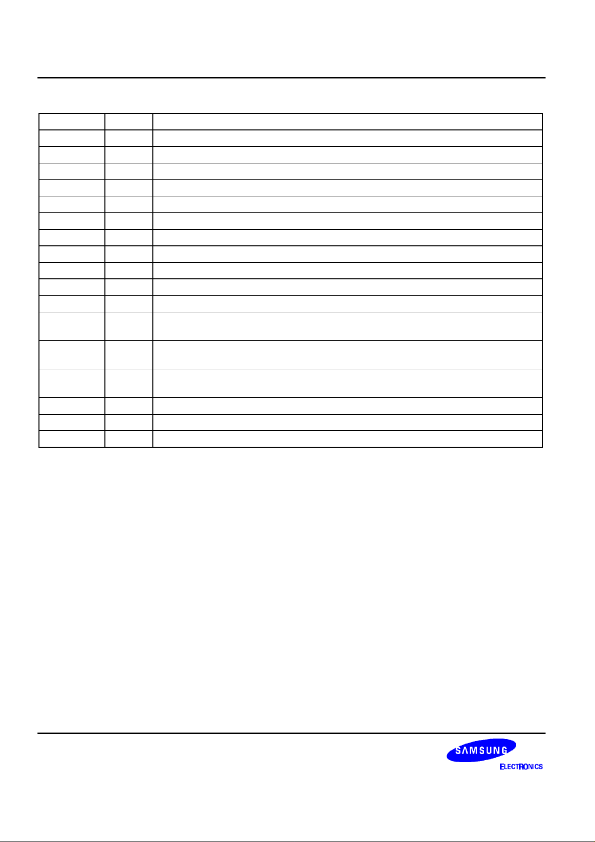
ELECTRICAL CHARACTERISTICS
ABSOLUTE MAXIMUM RATINGS
Item Symbol Spec. Unit
DC supply voltage VDDmax -0.3 to +7.0 V
DC input voltage: 3.3V (internal)
: 5.0V I/O
DC input current Iin
Storage Temperature Tstg -40 to 125
ELECTROSTATIC CHARACTERISTICS
Human Body Mode
Item Spec. Note
VDD positive/negative
VSS positive/negative
Vin3 -0.3 to 3.6 V
Vin5 -0.3 to 5.5
± 10
± 2000V
± 2000V
mA
°C
MM (Machine Model) Mode
Item Spec. Note
VDD positive/negative
VSS positive/negative
CDM Method
Item Spec. Note
VDD positive/negative
VSS positive/negative
± 300V
± 300V
±800V
±800V
10
DATA SHEET S5L9250B
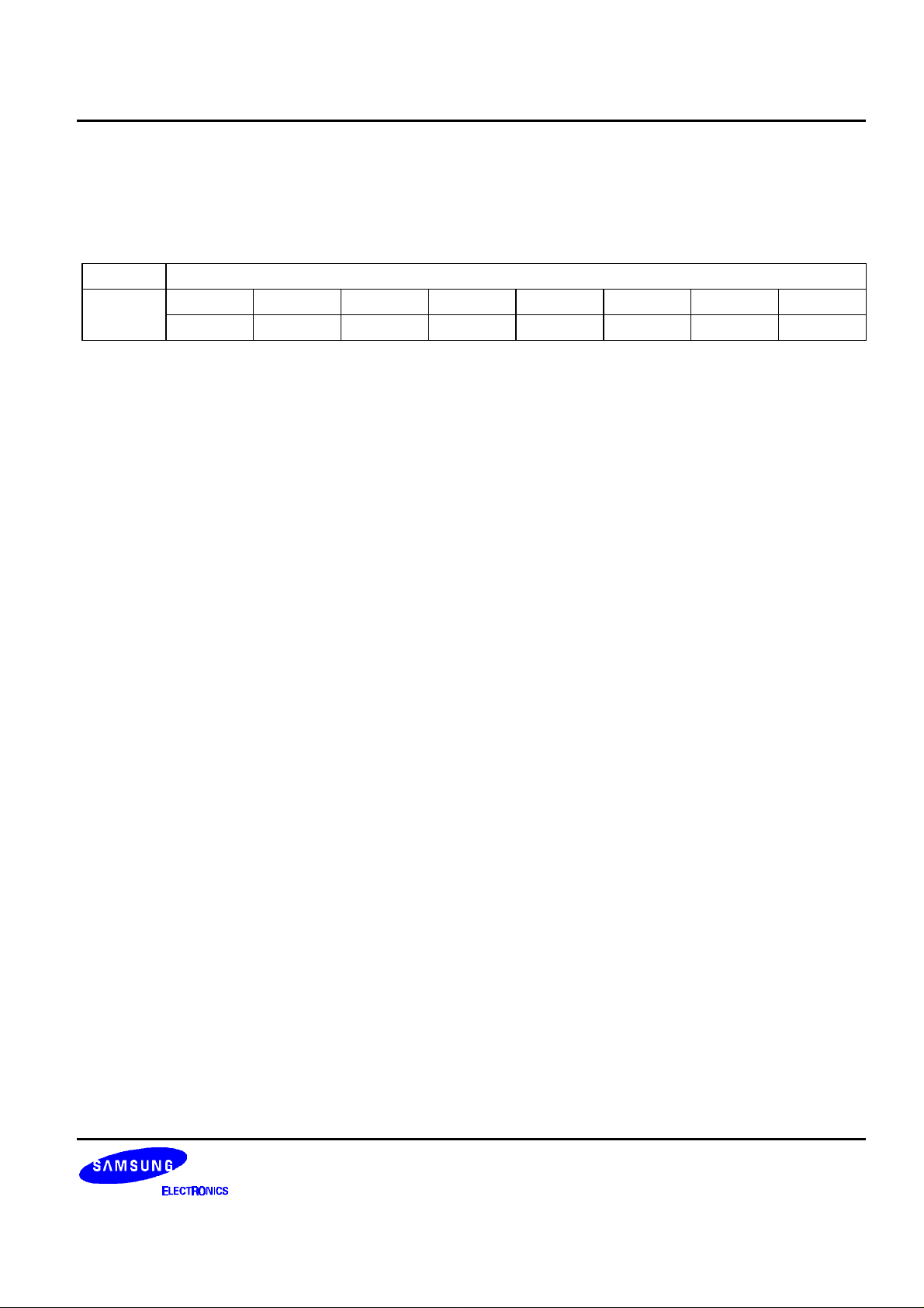
RECOMMENDED OPERATING CONDITIONS
No Item Symbol Spec. Unit
1 Operating temperature Topr 0 - 70
°C
2 DC supply voltage 3.3V VDD3 3.0 - 3.6 V
5.0V VDD5 4.75 5.25 V
DC CHARACTERISTICS: (VDD = 5V, VSS= 0V, Ta = 25°C)
ITEM Symbol Test Condition MIN TYP MAX Unit Note
'H' input voltage1
'L' input voltage1
'H' input voltage2
'L' input voltage2
'H' input current1
'L' input current1
'H' input current2
'L' input current2
'H' output voltage1
'L' output voltage1
Tri-state output leakage current
V
V
V
V
I
IH(1)
I
I
IH(2)
I
V
OH(1)
V
OL(1)
I
IH(1)
IL(1)
IH(2)
IL(2)
IL(1)
IL(2)
OZ
3.5 - - V
- - 1.5 V
2.0 - V
- 0.8- V
Vin = VDD -10 10 uA
Vin = VSS -10 10 uA
Vin = VDD 10 100 200 uA
Vin = VSS -200 -100 -10 uA
IOH = -2/-4/-8mA
IOL = 2/4/8mA
2.4 - - V
- - 0.4 V
Vout = VSS or VDD -10 - 10 uA
(1)
(1)
(2)
(2)
(3)
(3)
(4)
(5)
(6)
(6)
(7)
Quiescent supply current IDS Vin = VSS 100 uA
NOTES:
1. Related pins: All CMOS interface input terminals (PHIC)
All tri-state bi-directional pad's input terminals (PHBCT4)
2. Related pins: All CMOS schmitt trigger input terminals (PHIS, PHISU)
3. Related pins: All input terminals, bi-directional pad's input mode terminals.
4. Related pins: All input buffers with pull-down.
5. Related pins: All input buffers with pull-up.
6. Related pins: All output terminals.
7. Related pins: Tri-state output buffer (PHBCT4)
11

S5L9250B DATA SHEET
AC CHARACTERISTICS
DATA SLICER
Item Symbol Spec. Conditions
Min Typ Max Unit
RF input size Vrf 0.5 1.0 1.5 V
Input resistance Rin0 1.05 1.5 1.95 Kohm RES[2:0] = 0H
Rin1 1.4 2 2.6 Kohm RES[2:0] = 1H
Rin2 1.75 2.5 3.25 Kohm RES[2:0] = 2H
Rin3 2.1 3 3.9 Kohm RES[2:0] = 3H
Rin4 3.5 5 6.5 Kohm RES[2:0] = 4H
Rin5 4.55 6.5 8.45 Kohm RES[2:0] = 5H
Rin6 7 10 13 Kohm RES[2:0] = 6H
Rin7 28 40 52 Kohm RES[2:0] = 7H
Gain input resistance Ra1 8 10 12 Kohm
AMP offset Vosa -10 0 10 mV
Comparator open
Loop duty error DTe -2 0 2 %
COMP output resistance Roc 0 - 100 ohm
Switch on resistance Ron 0 - 100 ohm
Slice level fix
Output rang 1.24V - 2.04V
AMP gain Ra0 - 0 - Kohm INLG[2:0] = 0H
Ra1 4 5 6 Kohm INLG[2:0] = 1H
Ra2 8 10 12 Kohm INLG[2:0] = 2H
Ra3 32 40 48 Kohm INLG[2:0] = 3H
Ra4 72 90 108 Kohm INLG[2:0] = 4H
Ra5 150 190 228 Kohm INLG[2:0] = 5H
Ra6 232 290 348 Kohm INLG[2:0] = 6H
Ra7 392 490 588 Kohm INLG[2:0] = 7H
Output current = ±1m
Output current = ±1m
Vref ±15 Ls
12

DATA SHEET S5L9250B
EQUALIZER CONTROL
Item Symbol Spec. Conditions
MIN TYP MAX Unit
F/V gain Kfv 15.35 16.5 17.66 mV/%
F/V linearity FVlin -7 - 7 %
DAC resolution
∆VLS
26 mV DAC output range:
0.25 × VDD - 0.75 × VDD
DAC linearity
∆Li
-2 - 2 LSB
DAC velocity Ts 2.17 - 14.76 uS
Manual control voltage Output range: 0V - 3.3V
PLL
Item Symbol Spec Conditions
Min Typ Max Unit
Pump UP current absolute value IPU 2.1 2.3 2.5 mA
Pump DN current absolute value IPD -2.5 -2.3 -2.1 mA
Pump UP/DN current matching 1 IP1 - 5 10 %
Pump UP/DN current matching 2 IP2 - 5 10 %
VCO oscillating frequency high OSCH 200 - 250 MHz
VCO oscillating frequency low OSCL 20 - 50 MHz
Frequency division ratio 1 f40 - 45 - MHz
Frequency division ratio 2 f32 - 45 - MHz
Frequency division ratio 3 f28 - 30 - MHz
Frequency division ratio 4 f24 - 30 - MHz
Frequency division ratio 5 f20 - 22.5 - MHz
Frequency division ratio 6 f16 - 22.5 - MHz
Frequency division ratio 7 f8 - 15 - MHz
Frequency division ratio 8 f4 - 7.5 - MHz
Frequency division ratio 9 f1 - 1.875 MHz
CD lock check CDOK 2.8 3.8 - V
13

S5L9250B DATA SHEET
ARCHITECTURE DESCRIPTION
DIGITAL SERVO
Characteristics
• CD-ROM MAX 48X:
CLV: 4X, 8X
CAV: MAX 12X, 16X, 20X, 24X, 32X, 40X, 48X.
• Servo automatic adjustment:
F/T/SBAD offset, tracking balance, focus bias, F/T loop gain
• F/T input AGC feature that adapts to work with various disc types at an optimum level
• Track search algorithm using speed control method
• Algorithm for handling defects and shocks
• Generates various servo monitor signals: FOK, MIRR, TZC, and ATSC.
• Built-in 10-bit ADC (8ch division):
Samples FE/TE/various channels (1/16int.handling) three times at each fs.
• Built-in 4ch 10-bit DAC (for fod/trd/sled0, sled1 use)
• Disc discriminating data out (FEpk, SBADpk)
• Built-in 16-bit H/W track counter
• MICOM I/F feature: 8-bit parallel interface
• Serial interface with serial interface
Various automatic adjusting control signals, LD on/off, etc.
• Each loop filter's coefficient selection possible through MICOM:
focus normal/down, tracking normal/up, sled filter, various average value filter, BPF for ATSC use, BPF for
loop gain automatic adjustment, etc.
• Sampling frequency: 176.4kHz
• System clock: 33.8688MHz
• 3.3V & 5.0V dual power
14

DATA SHEET S5L9250B
Block Diagram
RFRP
RFCT
GPIO5/MIRR
SBAD
VREFI
CEI
PPUMP
XI
GPIO6/PHOLD
GPIO8/FOKB
DFCTI
ZRSTB
LOCK
SMONFGDIRROT
GPIO2/PS1
GPIO1/SSTOP
FELPF
TELPF
TZCA
GPIO4/TZCO
VREFO
TE
FE
AOUT
GPIO7/COUT
FOD
TRD
SLED0
SLED1
GPIO3/TPWM1
Analog & 10-bit
ADC
(bw1217l_cd)
Interface Block
Track Counter
10-bit DAC
(bw1244d)
Converter Block
PWM Generator
PLL
(al2002la)
Timing
Generator
DSP Core
SSP 1820
(OAKCORE)
ROM 8K
VROM_8192X16m32b2
I/O Interface BLock
RF Interface
Block
Micom Interface
Block
(Intel/Motorola)
RFDATA
RFCLK
RFEN
SENSE
WRB/RWB
RDB/DSB
ALE/RSB
CSB
AD[7:0]
15

S5L9250B DATA SHEET
Block Description
• Analog (A/D) interface block:
This block receives servo errors such as focus and tracking errors, and carries out input gain control
functions such as A/D conversion in order to heighten the rate of ADC deconstruction. It also has a TZC, a
MIRR comparator feature, a VREF generating feature, and a built-in 8ch dividing MUX.
• Timing generator:
The timing generator generates various timings used within the servo utilizing the external crystal
33.8688MHz. It also uses the built-in PLL's 40MHz as the basic signal for timing generation.
• I/O interface block:
This block accepts externally generated signals such as lock and SSTOP, and outputs internally generated
signals. It outputs various monitor signals such as ATSC and FOKB.
• RF interface block:
This block transmits various automatic adjustment outputs and data needed by the RF, such as
focus/tracking offset, TBAL output, AGC output, LD on/off, MICOM data, etc.
• MICOM interface block:
This block relays data between MICOM and 8-bit parallel.
• Track counter:
The track counter has a built-in 16-bit up/down counter to act as an accurate counter during jump.
It is 16-bit, allowing for full stroke counting.
• DA converter block:
This block uses a 10-bit DAC (R-string) to control the focus/tracking/sled0/sled1 at high resolution.
• Spindle PWM output:
This output is a 1-channel PWM output for spindle control (possible with sled)
• ROM:
This ROM is a servo program ROM with a built-in servo control program.
• DSP core for digital servo:
This block is central to the servo. It digitally handles various emergencies such as focus/tracking loop filter
handling, tracking jump, and sled move.
16
DATA SHEET S5L9250B
Register MAP and Bit Description
40x Servo Command Set for CD-ROM
Table 2. Register MAP and Bit Description
Name Code Description
STPcmd 00 Stop command: Stops jump or other auto adjustment-related actions.
DDTcmd 01 Disc detect command: Detects disc presence and carries out focus search.
FONcmd 02 Focus on command: Turns focus on through focus pull-in motion.
TONcmd 03 Track on command: Turns tracking on or off.
SLDcmd 04 Sled command: Controls the sled motor.
TRJcmd 05 Track jump command: Carries out track jump using the track counter.
SMVcmd 06 Sled move command: Carries out sled move using the track counter.
RPTcmd 07 Repeat jump command: Carries out interval jump using the track counter.
- 08 (Reserved).
- 09 (Reserved).
- 0A (Reserved).
CJNCcmd 0B CD jump number common command: Designates track number.
FGAcmd 0C Focus gain adjustment command: Automatically adjusts focus gain.
TGAcmd 0D Tracking gain adjustment command: Automatically adjusts tracking gain.
OFAcmd 0E Offset adjustment command: Automatically adjusts offset of TE/FE/SBAD.
TBAcmd 0F Tracking balance adjustment command: Automatically adjusts tracking balance.
HWofst 10 HWOFST (for center point control) adjustment command.
FBAcmd 11 Focus balance (= bias) adjustment command: Automatically adjusts focus balance.
ADScmd 12 Address setting command: Carries out upper address setting of RAM inside D-servo.
ADS1cmd 13 Address setting1 command: Sets and prepares to read lower address of RAM inside
D-servo.
DScmd 14 Data setting command: Decides address status after RAM write within D-servo.
DS1cmd 15 Data setting1 command: Upper data write in RAM within D-servo.
DS2cmd 16 Data setting2 command: Lower data write in RAM within D-servo.
JMDcmd 17 Jump mode select command: Designate jump-related initial value.
JMD1cmd 18 Jump mode1 select command: Designate jump-related initial value.
JMD2cmd 19 Jump mode2 select command: Designate jump-related initial value.
JMD3cmd 1A Jump mode3 select command: Designate jump-related initial value.
JMD4cmd 1B Jump mode4 select command: Designate jump-related initial value.
- 1C (Reserved).
EMEcmd 1D Emergency command: Various emergency-related setting command.
SenLcmd 1E If servo is active, sense is forcibly set to "L".
17
S5L9250B DATA SHEET
Table 2. Register MAP and Bit Description (Continued)
Name Code Description
CEoncmd 1F Center point servo controlling command
RFcmd 20 RF command set: Transmits RF address to send serial data to the RF IC.
RF1cmd 21 RF1 command set: Transmits RF data to send serial data to the RF IC.
HWCcmd 22 Hardware control command: Controls D-servo's H/W.
HWC1cmd 23 Hardware control1 command: Controls D-servo's H/W.
- 24 (Reserved).
- 25 (Reserved).
- 26 (Reserved).
- 27 (Reserved).
- 28 (Reserved).
ECOcmd 29 Eccentricity counter command: Counters eccentricity when off track.
ECScmd 2A Eccentricity compensation select command: Selects eccentricity compensation
method when off track.
ECCcmd 2B Eccentricity compensation control command: Controls eccentricity compensation
on/off.
FTSTcmd 2C Focus/tracking servo filter test command: Used for measuring the digital servo's
filter characteristics.
DPRWcmd 2D Direct port read/write command: Controls input/output of H/W inside D-servo.
DPWcmd 2E Direct port write command: Writes upper 8-bit data on the H/W inside D-servo.
DPW1cmd 2F Direct port write1 command: Writes lower 8-bit data on the H/W inside D-servo.
18
DATA SHEET S5L9250B
DETAILED BLOCK CHARACTERISTICS
Stop Command (STPcmd)
This command stops jump or auto adjustment-related servo activities, or enters into stop mode. The check
priority is RST>STOP>ABRT. LDON and IDLE have the same priority.
Code 1'st byte
00 D7 D6 D5 D4 D3 D2 D1 D0
RST STOP ABRT LDON 0 0 0 0
RST
0: Maintain current status.
1: Reset S/W (usually used during tray off).
STOP
0: Maintain current status.
1: Stop (automatically adjusted value does not change).
ABRT
0: Maintain current status.
1: Stop jump or adjustment-related servo activities.
LDON: Laser diode on/off bit (works only in stop mode).
0: Laser diode off.
1: Laser diode on.
D3-0: (Reserved). Must be set to "L".
19

S5L9250B DATA SHEET
Disc Detect Command (DDTcmd)
Laser diode is automatically turned on.
To detect if a disc is present, the focus actuator searches at the designated speed using the data RAM's
FSSPD(0x20) and FSDELTA(0x21). After this command, the Fepk (S-curve/2) data and SBpk (SBAD/2)'s
information are stored in the buffer so that SYSCON can read it.
Code 1'st byte
01 D7 D6 D5 D4 D3 D2 D1 D0
RPT DTM1, 0 0 FPKU 0 0 0
RPT: Repeat focus search motion (only possible when DTM1, 0 = 0, 0).
0: Carry out focus search motion only once.
1: Continue focus search motion until RPT = 0, or when STOPcmd's abort bit = 1 is accepted
(maintain sense = "L").
DTM1 -DTM0:
0: Carry out focus search once (auto).
01: Move the focus actuator to Vref position.
10: Raise focus actuator.
11: Lower focus actuator.
FPKU: S-curve detect location (set to 0 in manual mode).
0: Detect when down.
1: Detect when up.
• Search speed can be adjusted using the RAM's FSSPD(0x20), FSDELTA(0x21), FCNTmax(0x28), and
FCNTmin(0x29).
Search speed (1 period) = (FCNTmax-FCNTmin)*2*FSSPD/FSDELTA/Fs
• FE peak can be read through the MICOM interface after one search.
• The following are the data that MICOM can refer to after DDTcmd:
- FEpk: FE peak data (S-curve/2).
- SBpk: SBAD peak data (SBAD/2).
D15 D8 D7 D0
Fepk SBpk
20
DATA SHEET S5L9250B
Focus On Command (FONcmd)
This command carries out focus pull-in. The laser diode is turned on automatically. If focus is already on when
this command is received, no further actions are taken.
Code 1'st byte
02 D7 D6 D5 D4 D3 D2 D1 D0
0 FONU 0 0 PIM 0 0 0
FONU: Focus pull-in location.
0: After actuator up, pull-in when down.
1: After actuator down, pull-in when up.
PIM: Pull-in method.
0: Recognize FE. Use pull-in level's absolute value.
1: Recognize FE. Use pull-in level's FEPK percentage (can be set freely using kFEok(0xfe3e) and
kFEpi(0xfe3f)).
• Adjust search speed using the RAM's FSSPD(0x20), FSDELTA(0x21), FCNTmax(0x28), and FCNTmin
(0x29).
Search speed (1 period) = (FCNTmax-FCNTmin) * 2 * FSSPD/FSDELTA/Fs
• If FONcmd is accepted again during play (TRon), the tracking/sled is turned off.
21

S5L9250B DATA SHEET
Tracking On Command (TONcmd)
TONcmd is a tracking pull-in command.
If tracking is already on when this command is accepted, no further actions are taken.
Code 1'st byte
03 D7 D6 D5 D4 D3 D2 D1 D0
0 TON SLDX TFSB TOLB1-0 0 KICK
TON: Track on/off.
0: Off.
1: On.
SLDX : Sled servo on/off.
0: Sled off.
1: Turn sled servo on after a certain time interval from tracking on.
TFSB: Eccentricity compensation pull-in control bit during track pull-in.
0: Normal pull-in.
1: Eccentricity compensation pull-in (count between the edges of TZC and pull-in where
the frequency is low).
TOLB1-0: Lens brake during track pull-in and T/F gain control enable/disable.
Used for pull-in after jump using stepping motor.
0X: Off.
10: On (during normal pull-in, use the lens kick value for the lens brake time).
11: On (pull-in after the stepping motor feed kick).
KICK: KICK signal control (for stepping motor sled movement).
0: Set KICK signal to "L".
1: Set KICK signal to "H".
22
DATA SHEET S5L9250B
Sled On Command (SLDcmd)
SLDcmd is a sled motor control command. Bit check starts from the home bit.
Code 1'st byte
04 D7 D6 D5 D4 D3 D2 D1 D0
HOME SMOV SPLY 0 0 0 0 0
HOME: SLED HOME_IN mode select
0: Normal sled control mode.
1: Auto sled HOME_IN control mode.
When this bit is set, the sled motor moves backwards until it detects the LIMIT S/W. From then on, it moves
forward for the time designated by tSLDhomein.
SMOV, SPLY: Sled on/off and sled move control bit.
00: Sled off
01: Sled on
10: Sled forward move
11: Sled backward move
D4 to 0: Reserved. Must be set to "L".
When HOME = 1 (auto sled control mode), the SENSE is as shown below.
SENSE
LIMIT S/W
RVS
innermost
ON OFF
FWD
All limit sensor data when not in auto mode are output when focus is off while the sled is moving in either
direction. The limit sensor choice is made at JMD1cmd's JLIM1-0. It is "L" early in the command, but
becomes
"H" when it reaches either the innermost or outermost circumference.
23

S5L9250B DATA SHEET
Track Jump Command (TRJcmd)
TRJcmd is a track jump command used for track kick/brake jump and track speed control jump.
Code 1'st byte
05 D7 D6 D5 D4 D3 D2 D1 D0
DIR NUMS
DIR: Direction you want to move in using the track counter (TC).
0: Outward movement.
1: Inward movement.
NUMS: Number of upper tracks you want to move (0x00 - 0x7F).
• The lower jump track number is designated by CJNCcmd (0B).
24
DATA SHEET S5L9250B
Sled Move Command (SMVcmd)
SMVcmd is a sled move command that is used for sled kick/brake movement and sled speed control movement.
Code 1'st byte
06 D7 D6 D5 D4 D3 D2 D1 D0
DIR NUMS
DIR: The direction you want to move in using the track counter (TC).
0: Outward movement.
1: Inward movement.
NUMS: Number of upper tracks you want to move (0x00 - 0x7F).
• The lower Jump track number is designated by CJNCcmd (0B).
1. Repeat Jump Command (RPTcmd): (Reserved).
RPTcmd is an Interval track jump command that is used during a repeating jump.
Code 1'st byte
07 D7 D6 D5 D4 D3 D2 D1 D0
DIR NUMS
DIR: Direction you want to move in using the track counter (TC).
0: Outward movement.
1: Inward movement.
DIR: Direction you want to move in using the track counter (TC).
0: Outward movement.
1: Inward movement.
NUMS: Number of upper tracks you want to move (0x00 - 0x7F).
• The lower Jump track number is designated by CJNCcmd (0B).
• The interval frequency is designated by MICOM as 16 bit (0xfeef). interval freq.= sampling freq (fs)/MICOM
data
Example) If MICOM data is h'4000, 176 kHz (fs)/h'4000 (d'16384) = 9.2 Hz
25
S5L9250B DATA SHEET
CD Jump Number Common Command (CJNCcmd)
CJNCcmd is a command that designates the track number of TRJcmd, RPTcmd (reserved), and the lower track
number of SMVcmd.
Code 1'st byte
08 D7 D6 D5 D4 D3 D2 D1 D0
NUMS
NUMS: The number of lower tracks you want to move (0x01 - 0xFF).
Command input method for CD when executing sled move using SMVcmd.
: Input in the order, 06xx → 0Bxx.
Focusing Gain Adjustment Command (FGAcmd)
FGAcmd is a command that adjusts the auto focus gain. Use when focus servo is on, and tracking servo on or
off.
Code 1'st byte
0C D7 D6 D5 D4 D3 D2 D1 D0
FGud 0 0 0 0 0 0 TFGA
FGud: Auto focus gain update
0: No update
1: When changing Kfo, Kfuo after automatic adjustment, update according to the rate of change
during the automatic adjustment.
TFGA: Test mode for FGA
0: Normal FGA
1: Change focus gain once without regard to focus gain ok, then change back to the previous mode.
26
DATA SHEET S5L9250B
Tracking Gain Adjustment Command (TGAcmd)
TGAcmd is an auto tracking gain adjustment command.
Use while both focus servo and tracking servo are on.
Code 1'st byte
0D D7 D6 D5 D4 D3 D2 D1 D0
TGud 0 0 0 0 0 0 TFGA
TGud: Auto tracking gain update
0: No update
1: When changing Kto, Ktuo after automatic adjustment, update according to the rate of change during the
automatic adjustment.
TTGA : Test mode for TGA
0: Normal TGA
1: Change tracking gain once without regard to tracking gain ok, then change back to the previous mode.
27

S5L9250B DATA SHEET
Offset Adjustment Command (OFAcmd)
OFAcmd is an auto focus/tracking/SBAD offset Adjust command that measures and adjusts focus error, tracking
error, and SBAD signal. Lens location is selected by DDTcmd's DTM1-0.
Code 1'st byte
0E D7 D6 D5 D4 D3 D2 D1 D0
VREN RFRP SBEN TRD0 FOD0 CEIEN TEN FEN
VREN: VREF offset measurement enable bit.
0: Do not measure VREF offset.
1: Measure VREF offset.
RFRP: RFRP offset measurement enable bit.
0: Do not measure RFRP offset.
1: Measure RFRP offset.
SBEN: SBAD offset measurement enable bit.
0: Do not measure SBAD offset.
1: Measure SBAD offset.
TRDO: Tracking DAC offset adjustment.
0: Do not adjust.
1: Adjust.
FODO: Focus DAC offset adjustment.
0: Do not adjust.
1: Adjust.
CEIEN: Center error offset adjustment enable bit for center point servo.
0: Do not adjust offset.
1: Adjust offset.
TEN: Tracking offset adjustment enable bit.
0: Do not adjust tracking offset.
1: Adjust tracking offset.
FEN: Focus offset adjustment enable bit.
0: Do not adjust focus offset.
1: Adjust focus offset.
• After offset measurement, subtract the Vref offset from TRD and FOD.
28
DATA SHEET S5L9250B
Tracking Balance Adjustment Command (TBAcmd)
TBAcmd averages the MAX and MIN values of TE using eccentricity while the focus is on and tracking is off.
Always use before going into play (tracking on).
Code 1'st byte
0F D7 D6 D5 D4 D3 D2 D1 D0
0 0 0 0 0 0 0 TTBA
TTBA: Test mode for TBA
0: Normal TBA
1: Change tracking balance once without regard to tracking balance ok, then change back to
previous mode.
Hardware Offset Adjust Command (HWOFSTcmd)
HWOFSTcmd is the offset adjustment command for CEI, an input signal for center point control.
Code 1'st byte
10 D7 D6 D5 D4 D3 D2 D1 D0
0 0 0 0 0 0 0 THW0
Adjust the offset of RF's CEI output when HWOFSTcmd is accepted.
THWO: Test mode for HW offset.
0 : Normal HW offset
1: Carry out HW offset adjustment once without regard to HW offset OK, then change back to the previous
mode.
29

S5L9250B DATA SHEET
Focus Balance Adjustment Command (FBAcmd)
FBAcmd uses the RF envelop signal to end focus balance adjust when the RF signal is at its maximum. Always
use after focus pull-in.
Code 1'st byte
11 D7 D6 D5 D4 D3 D2 D1 D0
0 0 0 0 0 0 0 TFBA
TFBA: Test mode for FBA.
0 : Normal FBA.
1: Carry out focus balance once without regard to focus balance ok, then change back to the
previous mode.
Address Setting Command (ADScmd)
ADScmd directly accesses SRAM within the digital servo and sets the upper address during read/write. The lower
address is designated by ADS1cmd.
Code 1'st byte
12 D15 D14 D13 D12 D11 D10 D9 D8
ADDRESS
ADDRESS: Designates upper address of X,Y data memory.
• This command is used together with ADS1cmd that designates the lower address, and is thus always used as
2 bytes (ADScmd,ADS1cmd).
Address Setting1 Command (ADS1cmd)
ADS1cmd directly accesses SRAM within the digital servo and sets the lower address during read/write. It is
always used after ADScmd.
Code 1'st byte
13 D7 D6 D5 D4 D3 D2 D1 D0
ADDRESS
ADDRESS: Designates the lower address of X,Y data memory.
30
 Loading...