

1/3 INCH CCD IMAGE SENSOR FOR VGA COMPATIBILITY S5F333SZ03
ORDERING INFORMATION
H-CCD
INTRODUCTION
The S5F333SZ03 is an interline transfer progressive scan
type square pixel CCD area image sensor of 1/3 inch optical
format developed for VGA. The electron accumulation time
can be changed by the electronic shutter function and it is
possible to obtain a frame still image without a mechanical
shutter. High resolution and good color reproduction are
accomplished by using mosaic R, G, B primary color filters. It
is suitable for still cameras and PC input cameras.
FEATURES
• 330K Pixel Progressive-scan CCD
• High Vertical Resolution (480 TV lines)
• Square Unit Pixel for VGA Format
• No Substrate Voltage Adjustment
• No DC bias on Reset Clock
• R, G, B Mosaic On-Chip Color Filter
• Optical Size 1/3 inch Format
• Variable Speed Electronic Shutter
• Low Smear
• High Antiblooming
• Horizontal Register 5V Drive
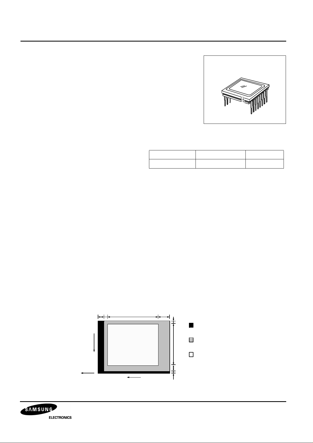
S5F333SZ03-LBB0 16Pin Cer - DIP -10 °C − +60 °C
16Pin Cer - DIP
Device Package Operating
STRUCTURE
• Number of Total Pixels: 692(H) × 504(V)
• Number of Effective Pixels: 659(H) × 494(V)
• Chip Size: 6.00mm(H) × 4.95mm(V)
• Unit Pixel Size: 7.40 µm(H) × 7.40 µm(V)
• Optical Blacks & Dummies: Refer to Figure Below
V-CCD
O UTPUT
16 2 659 31
Effective
Imaging
Ar ea
(Top vie w)
2 494 8 5
Dummy Pixels
O ptical Black Pixels
Effective Pixels
1
S5F333SZ03 1/3 INCH CCD IMAGE SENSOR FOR VGA COMPATIBILITY
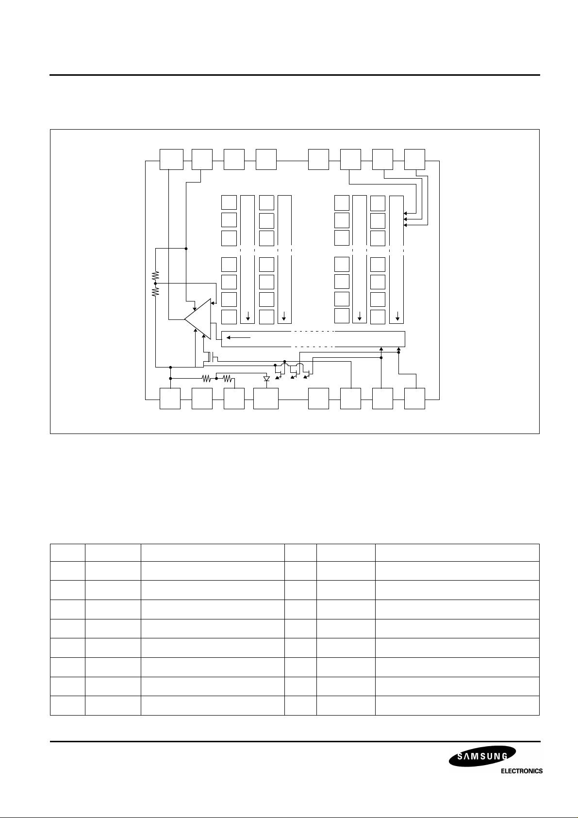
BLOCK DIAGRAM
(Top View)
8
V
OUT
9 10 11 12 13 14 15 16
V
DD
7 6 5 4 3 2 1
GND NC GND NC Φ
NC
G
R
G
G
R
G
GND
Vertical Shift Register CCD
Vertical Shift Register CCD
B
G
B
B
G
B
G
Horizontal Shift Register CCD
to substrate
Φ
SUB
G
R
G
G
R
G
R
V
Φ
L
V1
RS
Φ
V2
Vertical Shift Register CCD
G
G
GR
Φ
Vertical Shift Register CCD
B
B
B
B
H1
Φ
Φ
V3
H2
Figure 1. Block Diagram
PIN DESCRIPTION
Table 1. Pin Description
Pin Symbol Description Pin Symbol Description
1
2
3
Φ
Φ
Φ
V3
V2
V1
Vertical CCD transfer clock 3 9
Vertical CCD transfer clock 2 10 NC No connection
Vertical CCD transfer clock 1 11 GND Ground
4 NC No connection 12
5 GND Ground 13
6 NC No connection 14
7 GND Ground 15
8
V
OUT
Signal output 16
Φ
V
V
Φ
Φ
Φ
DD
SUB
L
RS
H1
H2
Output stage drain bias
Substrate clock
Protection circuit bias
Reset gate clock
Horizontal CCD transfer
Horizontal CCD transfer
2
1/3 INCH CCD IMAGE SENSOR FOR VGA COMPATIBILITY S5F333SZ03
ABSOLUTE MAXIMUM RATINGS
(1)
Table 2. Absolute Maximum Ratings
Characteristics Symbols Min. Max. Unit
Substrate clock voltage Φ
Supply voltage VDD, V
Vertical clock input voltage Φ
Φ
Φ
SUB
SUB
SUB
V1
- GND
- V
- V
OUT
- V
L
DD
OUT
- GND
ΦV2, ΦV3 - V
Φ
- Φ
V1
SUB
Φ
V2, ΦV3
- Φ
SUB
Horizontal clock input voltage ΦH1, ΦH2 - GND
ΦH1, ΦH2 - V
ΦH1, ΦH2 - Φ
L
L
SUB
-0.3 40 V
-0.3 40 V
-0.3 40 V
-0.3 17 V
-0.3 17 V
-0.3 32 V
-40
17
(2)
-40 32 V
-0.3 17 V
-0.3 17 V
-40
substrate DC bias
(3)
V
V
Output clock input voltage ΦRS - V
ΦRS - Φ
L
SUB
ΦRS - GND
Protection circuit bias voltage Φ
Operating temperature
Storage temperature
NOTE:
1. The device can be destroyed, if the applied voltage or temperature is higher than the absolute maximum rating voltage or
temperature.
2. VDD bias must be operated before reset pulse operation.
3. Substrate DC bias(OFD bias) must be operated before horizontal, reset pulse operation.
- V
SUB
GND - V
T
OP
T
STG
L
L
-0.3 17 V
-40
-0.3
substrate DC bias
(2)
17
(2)
-16 40 V
-0.3 17 V
-10 60 °C
-30 80 °C
V
V
3
S5F333SZ03 1/3 INCH CCD IMAGE SENSOR FOR VGA COMPATIBILITY
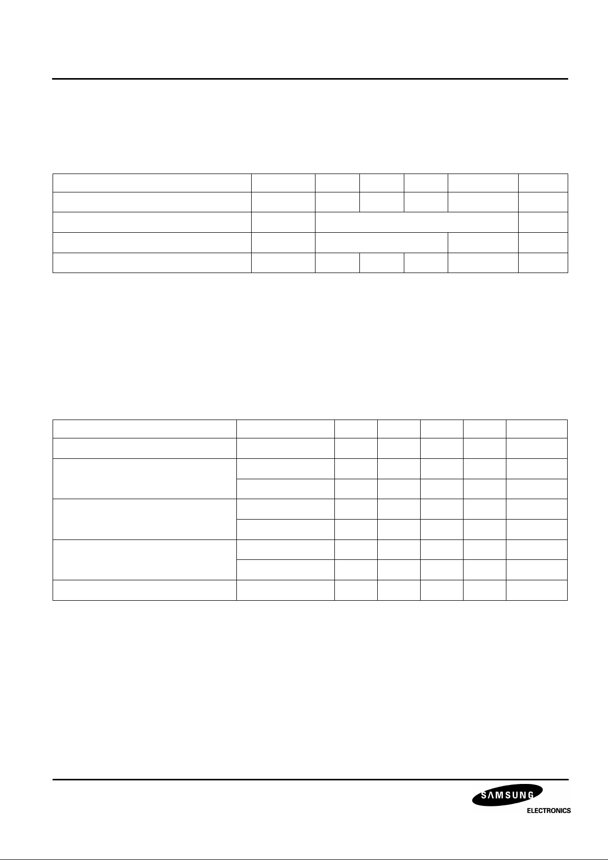
DC CHARACTERISTICS
Table 3. DC Characteristics
Item Symbol Min. Typ. Max. Unit Remark
Φ
V
V
I
DD
L
SUB
DD
Output stage drain bias
Protection circuit bias voltage
Substrate clock
Output stage drain current
NOTE: A DC bias (OFD bias) is generated within the CCD.
CLOCK VOLTAGE CONDITIONS
Table 4. Clock Voltage Conditions
Item Symbol Min. Typ. Max. Unit Remark
V
VM1
V
VH2
VL1
, V
~ V
~ V
Read-out clock voltage
Vertical transfer clock voltage V
14.55 15.0 15.45 V
The lowest vertical clock level
NOTE
5.0 mA
VH3
VM3
VL3
14.55 15.0 15.45 V High
-0.05 0.0 0.05 V Middle
-8.0 -7.5 -7.0 V Low
V
Horizontal transfer clock voltage V
V
HH1
HL1
Charge reset clock voltage V
Substrate clock voltage
V
, V
, V
RSH
V
RSL
ΦSUB
HH2
HL2
4.75 5.0 5.25 V High
-0.05 0.0 0.05 V Low
4.75 5.0 5.25 V High
-0.05 0.0 0.05 V Low
21.5 22.5 23.5 V Shutter
4
1/3 INCH CCD IMAGE SENSOR FOR VGA COMPATIBILITY S5F333SZ03
V
=
VVL-0.3V
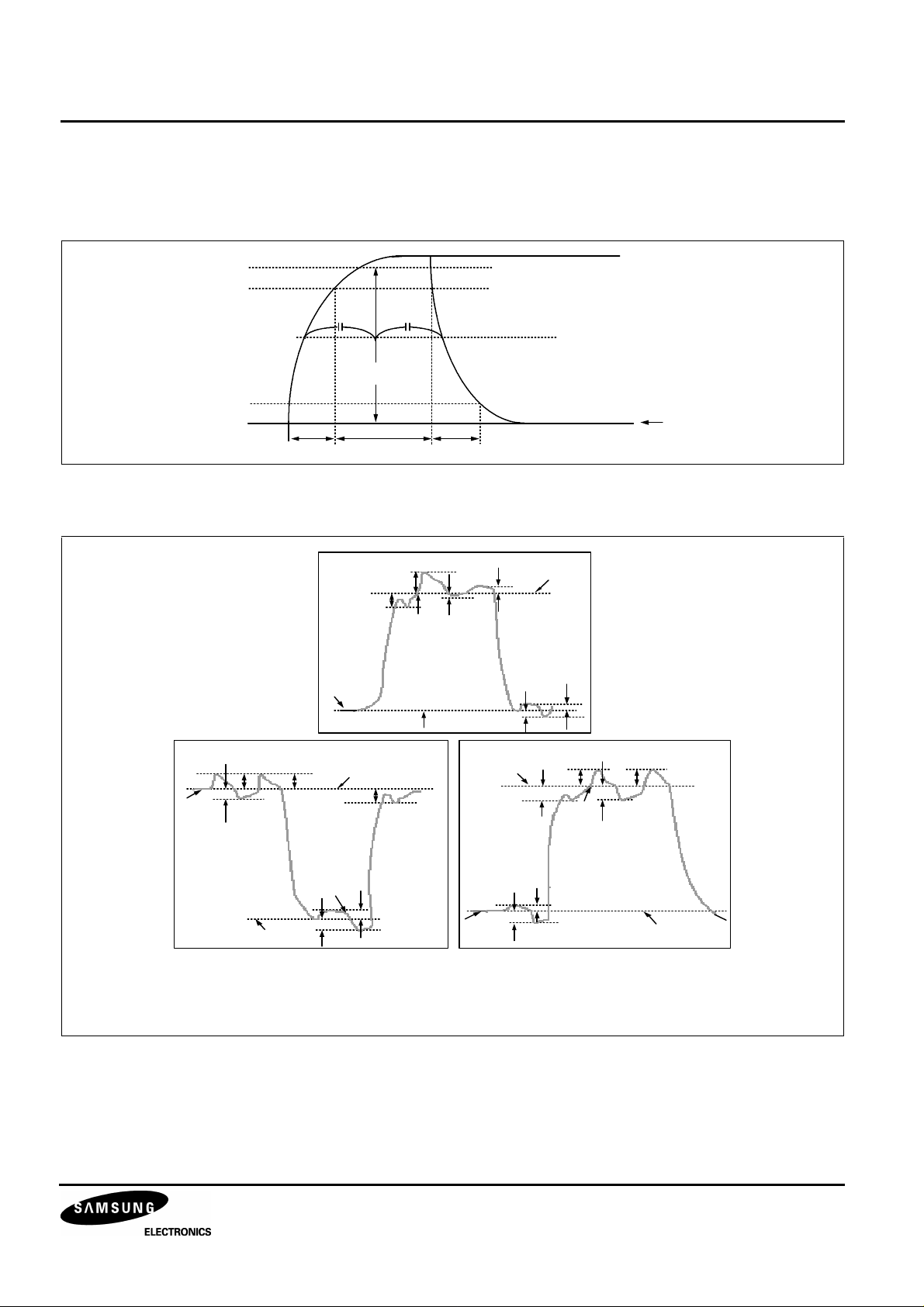
DRIVE CLOCK WAVEFORM CONDITIONS
Read Out Clock Waveform
100%
90%
V
VH2,VVH3
10%
0%
Vertical Transfer Clock Waveform
tr twh tf
0V
¥Õ
V VH2
V 2
V V HH VVH H
V
VH L
V
VL
¥Õ
V 1
V V HL
V VL 3
V
VH
V
VH L
V VL H
V VL 2
V VL L
V
= V
V H
VH 2
VV L = ( V V L 1 + VV L 3)/ 2
V¥ÕV= V
VH n
V V HH
- V
VL n (n =1~3)
V
V V HL
V
VH3
VHH
V
VH
V V L H
V
V VL
VL L
V
¥Õ
V 3
V
VH
V V HH
V
VHL
V V H4
VHH
V
VH L
V VL H
V
VL L
V
VL 4
V
= V
V H
+ 0. 3V
VH H
V
VL
VV H L = V V H - 0.3 V
V
= V
V L
+ 0. 3V
VL H
VL L
5
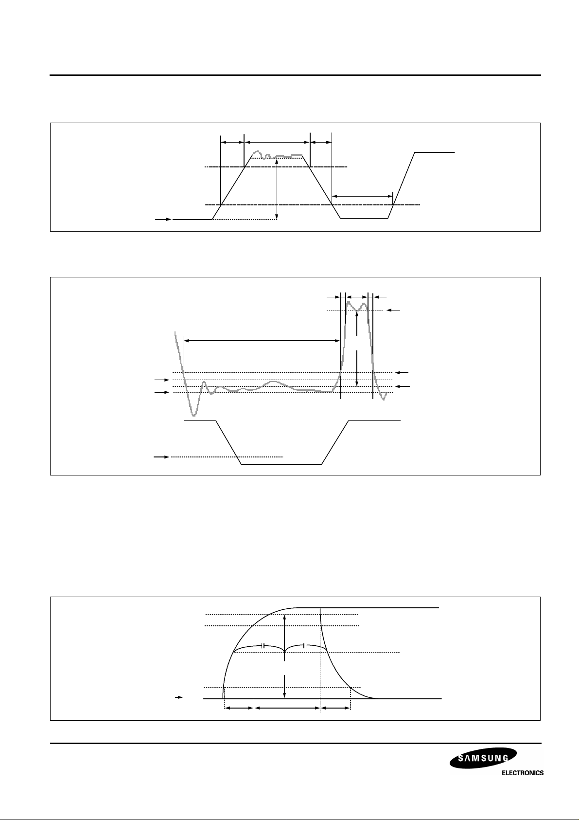
S5F333SZ03 1/3 INCH CCD IMAGE SENSOR FOR VGA COMPATIBILITY
V
Horizontal Transfer Clock Waveform Diagram
90%
10%
HL
Reset Gate Clock Waveform Diagram
RG waveform
V
RGLH
V
RGLL
tr twh
twl
Point A
V¥Õ
tf
H
twl
twh tftr
V
RGH
V
¥Õ
RG
V
+ 0.5V
RGL
V
RGL
¥Õ
H1 waveform
10%
V
is the maximum value and V
RGLH
in the diagram about to RG rise
V
RGL
= (V
RGLH
+ V
RGLL
)/2, V
Substrate Clock Waveform
V
SU B
FRG
100%
90%
10%
0%
is the minimum value of the coupling waveform in the period from Point A
RGLL
= V
RGH
- V
RGL
¥Õ
V
SU B
twhtr tf
6
 Loading...