

Samsung S5C7212X01-E0R0 Datasheet
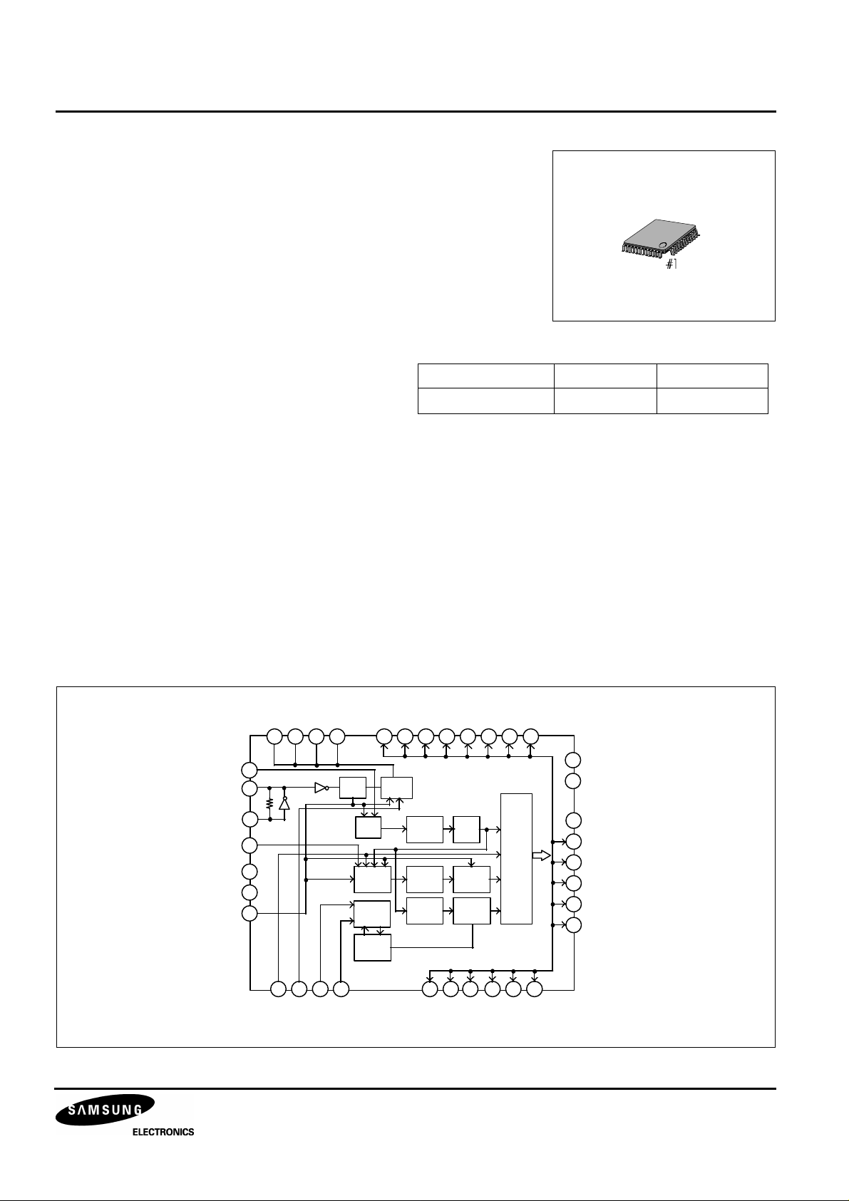
TIMING & SYNC. GENERATOR FOR B/W CCD S5C7212X01
ORDERING INFORMATION
INTRODUCTION
The S5C7212X01 is a CMOS integrated circuit designed for making various
timing pulses for B/W CCD camera.
FEATURES
• Compatible with both EIA and CCIR mode
( EIA : S5F325NW02 / S5F325NU02
CCIR : S5F329PW02 / S5F329PU02 )
• Built in auto iris function (Electronic Exposure)
• Mirror mode timing generation
• Field interlace mode only
• Timing and sync one chip IC
• Oscillation frequency
EIA : 19.06992MHz, CCIR : 18.93750MHz
Device Package Operating
S5C7212X01-E0R0 48-QFP-0707
48-QFP-0707
-20 °C − 75 °C
APPLICATION
• B/W CCD Camera
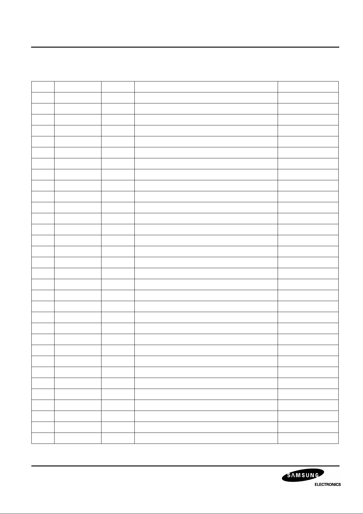
BLOCK DIAGRAM
CL
X2
X1
TS2
TS1
TS0
PWR
ϕH4
ϕH3
ϕH1
38 37 36 35 30 29 28 27 26 25 2433
43
41
40
45
46
47
48
2 3 41 127 8 9 10 11
ϕH2
1/2
1/606
High/Low
Control
1/525
or
1/625
Shutter
Speed
ROM
RG
GATE1
XSUB
XV2
Horizontal
ROM
Vertical
ROM
Shutter
Speed
Count
XV1
XSG1
F/F
F/F
Shutter
Speed
Control
XV3
XSG3
GATE2
XV4
22
SHP
21
SHD
CLP1
18
CLP2
17
CLP3
16
DFDO
15
CLEN
14
WIN
13
MD2
MD1
EE1
EE2
FLD
PBLK
CSYNC
CBLK
VD
HD
1
S5C7212X01 TIMING & SYNC. GENERATOR FOR B/W CCD
PIN DESCRIPTION
No Symbol I/O Description Remark
1 MD2 I CCIR/EIA mode selection * Information (1)
2 MD1 I NORMAL/MIRROR mode selection * Information (1)
3 EE1 I EE mode control input 1 * Information (2)
4 EE2 I EE mode control input 2 * Information (2)
5 VSS1 - Ground
6 VDD1 - +5V
7 FLD O Field separation pulse
8 PBLK O Pre - blanking pulse
9 CSYNC O Composite Sync.pulse
10 CBLK O Composite Blanking pulse
11 VD O Vertical driving pulse
12 HD O Horizontal driving pulse
13 WIN O Window pulse
14 CLEN O 1/2 HD frequency pulse
15 DFDO O 1/2 VD frequency pulse
16 CLP3 O Clamp pulse 3 (Dummy black level)
17 CLP2 O Clamp pulse 2 (Optical black level)
18 CLP1 O Clamp pulse 1 (Optical black level)
19 VSS2 - Ground
20 VDD2 - +5V
21 SHD O Data Sample & Hold pulse
22 SHP O Pre - Charge Sample & Hold pulse
23 VSS3 - Ground
24 XV4 O Vertical transfer clock 4
25 XSG3 O Read out Pulse 3
26 V3 O Vertical transfer clock 3
27 XSG1 O Read out Pulse 1
28 XV1 O Vertical transfer clock 1
29 XV2 O Vertical transfer clock 2
30 XSUB O Shutter speed control for auto iris
31 VDD3 - +5V
32 VSS4 - Ground
2
TIMING & SYNC. GENERATOR FOR B/W CCD S5C7212X01
No Symbol I/O Description Remark
33 ϕRG O Reset gate pulse
34 VDD4 - +5V
35 ϕH2 O Horizontal transfer pulse 2 ( Mirror mode)
36 ϕH1 O Horizontal transfer pulse 1 ( Normal mode’H1’)
37 ϕH3 O Horizontal transfer pulse 3 ( Normal mode’H2’)
38 ϕH4 O Horizontal transfer pulse 4 ( Mirror mode )
39 VSS5 - Ground
40 X1 I Oscillation clock Input
EIA : 19,069928MHz CCIR : 18.93750MHz
41 X2 O Oscillation clock Output
42 VDD5 O +5V
43 CL O 1/2 Oscillation clock
EIA : 9.53496MHz CCIR : 9.46875MHz
44 VSS6 - Ground
45 TS2 I Test Input 2
46 TS1 I Test Input 1
47 TS0 I Test Input 0
48 PWR - Power On Reset
Information 1) MD2 and MD1 mode selection ( Pull - down )
MD2 MD1 MODE
L EIA NORMAL
L
H EIA MIRROR
L CCIR NORMAL
H
H CCIR MIRROR
Information 2 ) EE2 and EE1 shutter speed mode selection ( Pull - up )
EE2 EE1 MODE
L
L SHUTTER SPEED STOP
H SHUTTER SPEED UP
L SHUTTER SPEED DOWN
H
H SHUTTER SPEED STOP
3
S5C7212X01 TIMING & SYNC. GENERATOR FOR B/W CCD
ABSOLUTE MAXIMUM RATINGS
Characteristics Symbol Value Unit
Supply Voltage V
Input Voltage V
Output Voltage V
Operating Temperature T
Storage Temperature T
CC
I
O
OPR
STG
VSS-0.5 − VDD+0.5 V
VSS-0.5 − VDD+0.5 V
7 V
-20 − +75 °C
-55 − +150 °C
ELECTRICAL CHARACTERISTICS
(VDD=5V, Ta=25°C, unless otherwise specified)
Characteristics Symbol Test Condition Min Typ Max Unit
Supply Voltage V
Input Voltage 2 V
Output Voltage 1 V
V
Output Voltage 2 V
(CL, RG, SHP, SHD) V
Output Voltage 3 V
(H1, H2, H3, H4) V
DD
IH
V
OH1
OL1
OH2
OL2
OH3
OL3
IL
IOH1 = -2mA VDD-0.5 - - V
IOL1 = 4mA - - 0.6 V
IOH2 = -4mA VDD-0.5 - - V
IOL2 = 8mA - - 0.6 V
IOH3 = -8mA VDD-0.5 - - V
IOL3 = 8mA - - 0.6 V
- 4.75 5.0 5.25 V
- 0.7V
DD
- - - 0.3V
- - V
DD
V
4
TIMING & SYNC. GENERATOR FOR B/W CCD S5C7212X01
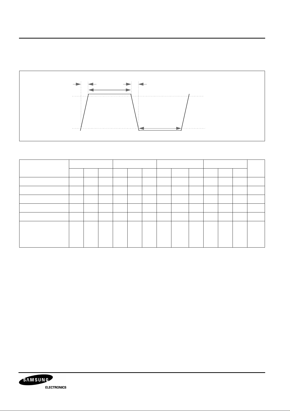
AC CHARACTERISTICS
tr
twh
90%
10%
tf
0.9VDD
twl
0.1V
DD
twh twl tr tf
PULSES
Unit
Min. Typ. Max. Min. Typ. Max. Min. Typ. Max. Min. Typ. Max.
XSG1, XSG3 2.3 2.5 0.5 0.5 us
XV1, XV2, XV3, XV4 0.015 0.24 us
H1, H2, H3, H4 26 32 26 32 11 12 11 12 ns
RG 11 13 51 5 5 ns
XSUB 1.5 2.0 0.5 0.5 us
SHP, SHD, CLP1,
CLP2, CLP3, DFD0,
CLEN, WIN, HD, VD,
CBLK, CSYNC, FLD
13 14 16 13 14 16 ns
5
S5C7212X01 TIMING & SYNC. GENERATOR FOR B/W CCD
OPERATING PRINCIPLES & METHODS
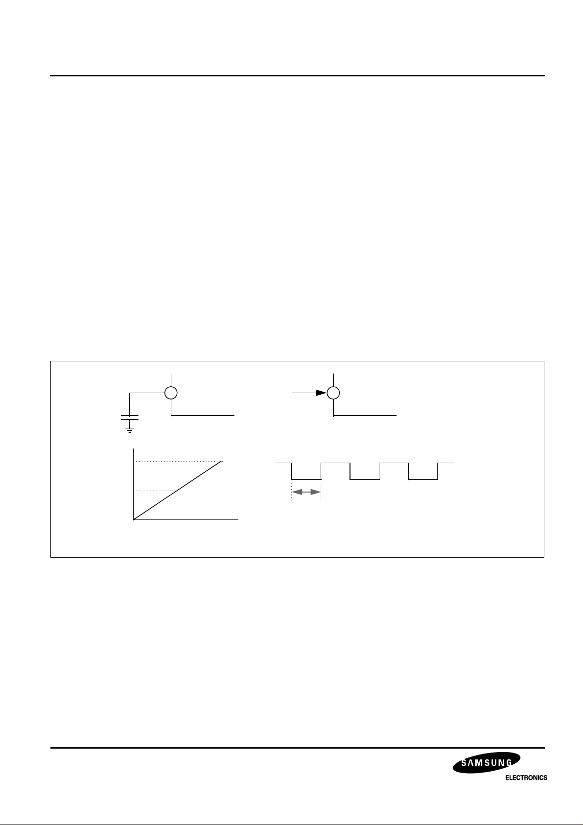
POWER ON RESET
S5C7212X01 has two reset methods. The one is power on reset and the other is normal reset.
When user wants to use power on reset, which generates an automatic reset signal that is needed to initialize the
S5C7212X01 internal system when power is on, user should connect the 1000pF capacitor to the PWR ( pin 48 )
terminal.
Power on reset system has an internal 100Kohm pull up resister. So, user can control reset signal timing when
user changes the value of the capacitor, which is connected to the PWR terminal.
When user wants to use normal reset, user should remove the capacitor from the PWR terminal, and supply the
reset signal to the PWR terminal.
KS7212
S5C7212X01
48 48
1000pF
2.4 ~
2.6 V
Fig. 1 POWER ON RESET Fig. 2 NORMAL RESET
RESET
SIGNAL
840ns
KS7212
S5C7212X01
When using the u-Com system, the reset signal can be supplied three times, and times of 1 signal should be
larger than four times of CL clock.
6
 Loading...