

Samsung S5A1903X01-E0R0 Datasheet
DATA PROCESSOR S5A1903X01
INTRODUCTION
The S5A1903X01 implements the voice intelligibility processor (VIP).
The VIP is a signal processing algorithm designed to increase the
intelligibility of human speech in a high ambient noise environment.
Unlike noise cancellation or adaptive speech filtering systems, VIP
operates on the speech signal only and is totally independent of the
noise. This approach makes speech clearer and easier to understand
regardless of the characteristics of the noise source, and eliminates
the need for processing of the noise signal.
In addition to VIP, the S5A1903X01 includes voice equalizer. The
equalizer is composed of four different frequency bands, and each
band is controlled between +12dB and -12dB. Thus, it can be used to
compensate of speaker characteristics.
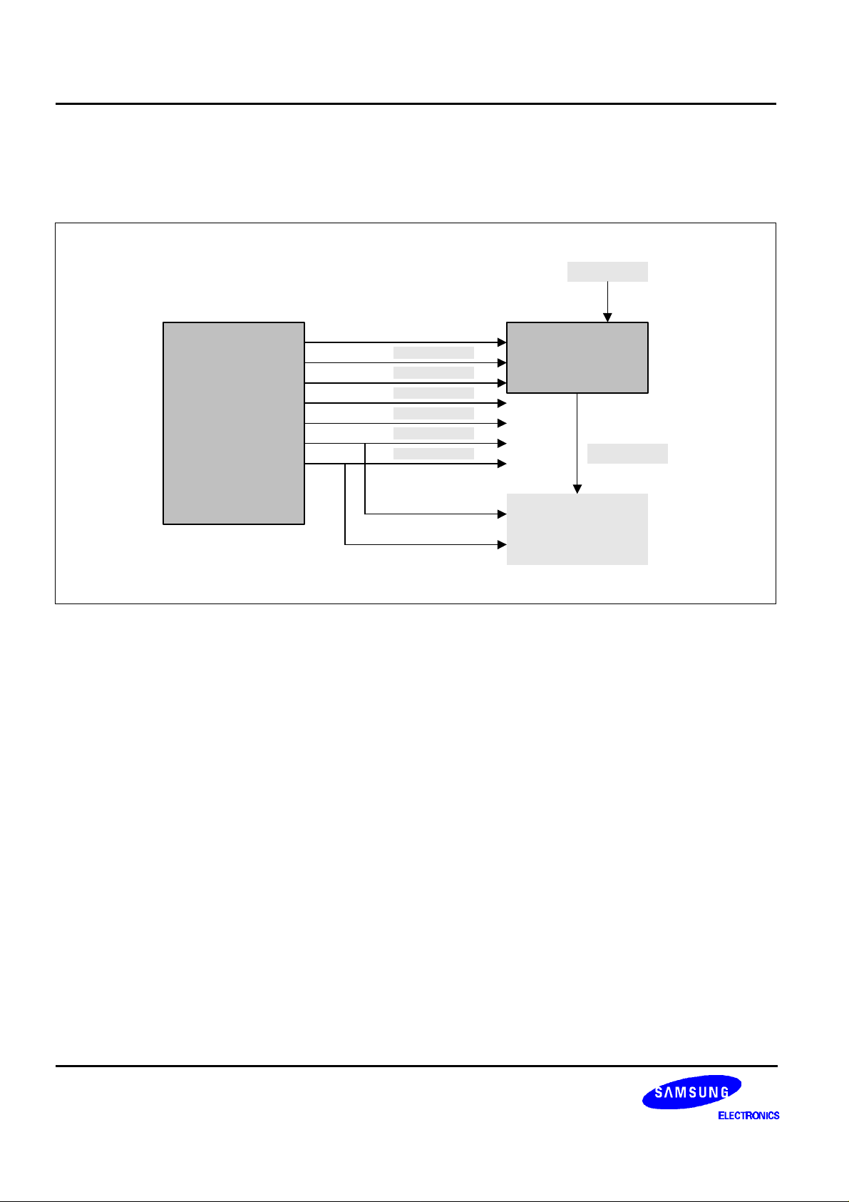
The Figure 1 shows how the S5A1903X01 interfaces to Vocoder and Codec in cellular phone.
32-LQFP
MAIN FEATURES
• IP Mode
• Equalizer Mode
• 16-bit Fixed Point DSP Core
• Two Internal 256-word Data RAM
• 2K-word Internal Program ROM
• Wide Range of System Clock
: 8 - 40 MHz
— PCM Input/ Output Interface
— I2C Host Interface
— Low Power Consumption
less than 4mA in working mode
10uA in sleep mode
— Packages: 32-LQFP/ 32-BCC
— 3V Single Power Supply
ORDERING INFORMATION
Device Package Temperature Range
S5A1903X01-E0R0 32 LQFP 0°C − 70°C
APPLICATIONS
• Cellular Phone
• Wireless and Traditional Telephone
1
S5A1903X01 DATA PROCESSOR
BLOCK DIAGRAM
System Block Diagram
CKIN
VOCODER
RESB
SCL
SDA
DIN
FS
MCLK
VIP
DOUT
VOICE
CODEC
2
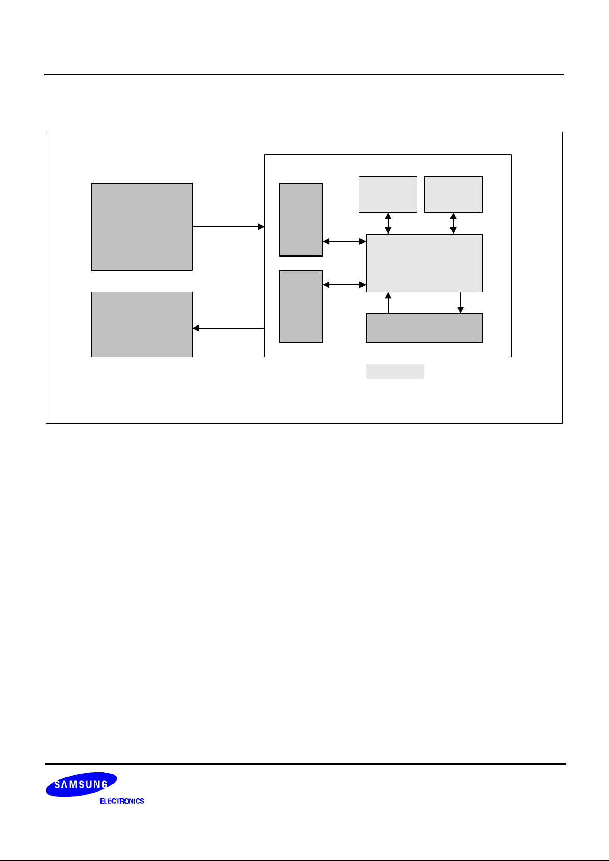
DATA PROCESSOR S5A1903X01
Chip Block Diagram
MSM
VOCODER
CODEC
I2C
I/F
Digital
I/F
SRAM
256
VIP
SRAM
256
SSP1611
P.ROM 2K
NOTE: Not Scaled
3
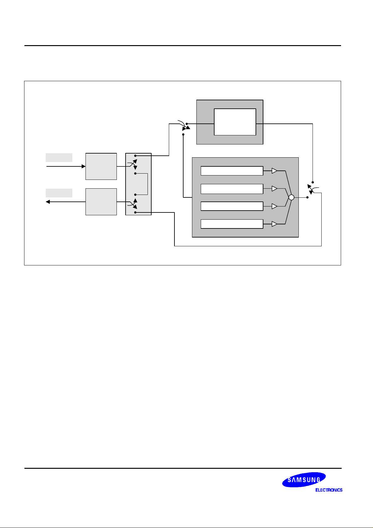
S5A1903X01 DATA PROCESSOR
Functional Block Diagram
Voice
Intelligibility
Proces
DIN
DOUT
PCM
INPUT
I/F
PCM
OUTPUT
I/F
BPF (Center: 300HZ)
BPF (Center: 600HZ)
+
BPF (Center: 1.2kHZ)
HPF (Cutoff: 2.4kHZ)
4
DATA PROCESSOR S5A1903X01
GPO0
VDD1
GPI0
GPI1
GPI2
GPI3
GND1
RESB
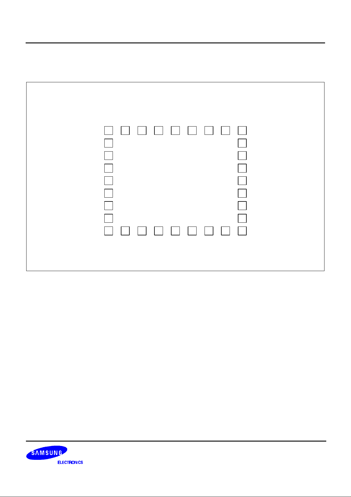
PIN ASSIGNMENTS
TCLKDR
TIDR
TSHFTDR
GND3
TUPDDR
TSELDR1
TSEKDR0
VDD3
SAS
VDD4
TODR
GPO3
GPO2
DOUT
GND4
GPO1
25
24 23 22 21 20 19 18
26
27
28
S5A1903X01
29
30
31
32
1 2 3 4 5 6 7 8 9
32BCC
(Top View)
17
16
15
14
13
12
11
10
SCL
SDA
GND2
CKIN
VDD2
MCLK
DIN
FS
5
S5A1903X01 DATA PROCESSOR
PIN DESCRIPTION
Related Block PIN NAME PIN NO. I/O Description
RESB 8 I Reset: Active Low
HIU SDA 15 I/O I2C Serial Data
SCL 16 I I2C Serial Clock
SAS 17 I I2C Address Selection
DIN 10 I 16 Bit PCM Serial Data In
CIU DOUT 30 O 16 Bit PCM Serial Data Out
FS 9 I PCM Data Frame Sync.
MCLK 11 I PCM Data Bit Clock
System CKIN 13 I System Clock (9.84MHz)
GPI0 3 I Test Pin0 (Host INT. Indicator)
GPI1 4 I Test Pin1(0:No Fade, 1:Fade)
GPI2 5 I Test Pin2 (0:RAM Test)
GPI3 6 I Test Pin3 (0:Codec Bypass)
TSELDR0 19 I Test Pin for JTAG
TSELDR1 20 I Test Pin for JTAG
TEST TUPDDR 21 I Test Pin for JTAG
TSHFTDR 23 I Test Pin for JTAG
TIDR 24 I Test Pin for JTAG
TCLKDR 25 I Test Pin for JTAG
TODR 27 O Test Pin for JTAG
GPO0 1 O Host Ack. Pin
GPO1 32 O Host Test Output
GPO2 29 O Host Test Output
GPO3 28 O Host Test Output
Power
Ground
VDD1, VDD2
VDD3, VDD4
GND1, GND2
GND3, GND4
2, 12,
18, 26
7, 14,
22, 31
P Digital Power (+3.0V)
G Digital GND
6
 Loading...