

Samsung S5A1901H02-Q0R0 Datasheet

AUDIO EFFECT PROCESSOR S5A1901H02
PRODUCT OVERVIEW
OVERVIEW
The S5A1901H02, Audio Effect Processor, reproduces vivid sound of
certain places and dynamic sound of movies. The S5A1901H02 has
over 15 sound effect modes including two kinds of Karaoke mode. In
addition to the sound modes, the S5A1901H02 provides mic-echo,
vocal canceller, loudness function, graphic equalizer, spectrum analyzer interface, tone control and volume/balance control so that it can
satisfy various sound requirements of audio systems including TV,
stereo audio systems, etc. Furthermore, the S5A1901H02 has built-in
16 bit stereo Σ−∆ ADC and DAC for easy application. The
S5A1901H02 also includes two digital source interface blocks and a
host interface block supporting normal microcontroller and I2C bus
interfaces.
KEY FEATURES
• Over 15 Sound Effect Modes including two kinds of Karaoke mode
100−QFP−1420C
• 3/5/7-band Graphic Equalizer and 5/7-band Spectrum Analyzer Interface
• Mic-Echo, Loudness Function and Vocal Canceller
• Digital Volume/Balance/Tone Control
• Fader Function for Car Stereo System
• Programmable Sound Mode
• 33 MIPS 16 bit fixed point DSP Core (SSP1610)
• Built-in Stereo 16 bit Σ−∆ ADC and DAC
• External Clock: 16.9344MHz
• Sampling Frequency: 44.1kHz
• Support Various Digital Audio Interface Formats
• Normal Microcontroller Interface and I2C Bus Interface
• 0.5 Kword Internal Data RAM and 6 Kword Delay Memory for Sound Effect
• 6 Kword Internal Program ROM and 0.5 Kword Parameter ROM for Movie Mode
• 5 V Single Power Supply
• 0.5µm Triple Metal CMOS Process
• Package: 100 QFP
ORDERING INFORMATION
Device Package Temperature Range
S5A1901H02-Q0R0 (Audio Effect Processor) 100−QFP−1420C 0°C − 70°C
1

S5A1901H02 AUDIO EFFECT PROCESSOR
APPLICATIONS
• CD Player
• Video CD
• TV
• Karaoke System
• Car Stereo System
• General Stereo Audio Systems
2

AUDIO EFFECT PROCESSOR S5A1901H02
TYPICAL APPLICATION
Spectrum Analyzer
Digital Source
µ
-COM
AEP
for Recording
Analog Source
Digital Source
Vol Bal Tone
Spectrum Analyzer
µ
-COM
AEP
Vol Bal Tone
Sound Effect & Karaoke Mode
( ProLogic )
with ProLogic
Figure 1. S5A1901H02 Typical Application
3

S5A1901H02 AUDIO EFFECT PROCESSOR
BLOCK DIAGRAM
RESB
SPWDN
TINT1
CONTROL & TEST
LOGIC
Program
ROM
Data
RAM
DSP
Data
RAM
CIU
CRU
DSIU1
DSIU2
16 Bit Stereo Σ -
CODEC
DLRCKO2,DBCKO2,
DSDO2
DLRCKI2,DBCKI2,
DSDI2
ALI,ARI
∆
CMCLKS
ALO,ARO
VREF,VREFI
DLRCKI1,DBCKI1,
DSDI1
DLRCKO1,DBCKO1
DSDO1
CLK1
CLKS
CLK2
(33.8688MHz)
(16.9344MHz)
CGU
XI
MCLK
CLK3
XO
(11.2896MHz)
CLKO
MIU
SEIU
SAIU
HIU
I2C
* CRU : Configuration Register Unit
* CIU : Built-in CODEC Interface Unit
* DSIU1 : Digital Source Interface Unit 1
* DSIU2 : Digital Source Interface Unit 2
* MIU : Memory Interface Unit
* SEIU : Stereo Enhancement Interface Unit
* HIU : Host Interface Unit
* SAIU : Spetrum Analyzer Interface Unit
* I2C : I2C Interface Unit
* CGU : Clock Generation Unit
Delay RAM
3-D
Parameter ROM
HDATA
HWEB,HCLK
HMS,SAS
SDA
SCL
HACK
Figure 2. S5A1901H02 Block Diagram
4
AUDIO EFFECT PROCESSOR S5A1901H02
DLRCKO2
PIN ASSIGNMENT
VCC2
ALI
ARI
VREF
VREFI
VSS1
VCC1
ALO
ARO
VSS2
VDD13
GND13
VDD0
GND0
NC
NC
NC
NC
VDD1
GND1
NC
NC
NC
NC
VDD2
GND2
NC
NC
NC
NC
NC
NC
NC
NC
VDD3
GND3
SAS
RESBNCNCNCNCNCNC
99
98
97
96
100
1
2
3
4
5
6
7
8
9
10
11
12
13
14
15
16
17
18
19
20
21
22
23
24
25
26
27
28
29
30
959493
(Audio Effect Processor)
92
91
90
S5A1901H02
89
VDD12
GND12NCNCNCNC
88
87
86
85
84
83
82
81
80
NC
79
NC
78
VDD11
77
GND11
76
NC
75
NC
74
NC
73
NC
72
GND10
71
VDD10
70
MCLK
69
CLKS
68
XI
67
XO
66
GND9
65
VDD9
64
CLKO
63
NC
62
SPWDN
61
NC
60
TINT1
59
HACK
58
GND8
57
VDD8
56
DLRCKI1
55
DBCKI1
54
DSDI1
53
GND7
52
VDD7
51
DLRCKO1
31
HMS
32
HCLK
33
34
35
HWEB
VDD4
HDATA
363738
GND4
SCL
SDA
39
VDD5
40
GND5
41
DSDI2
42
43
DBCKI2
DLRCKI2
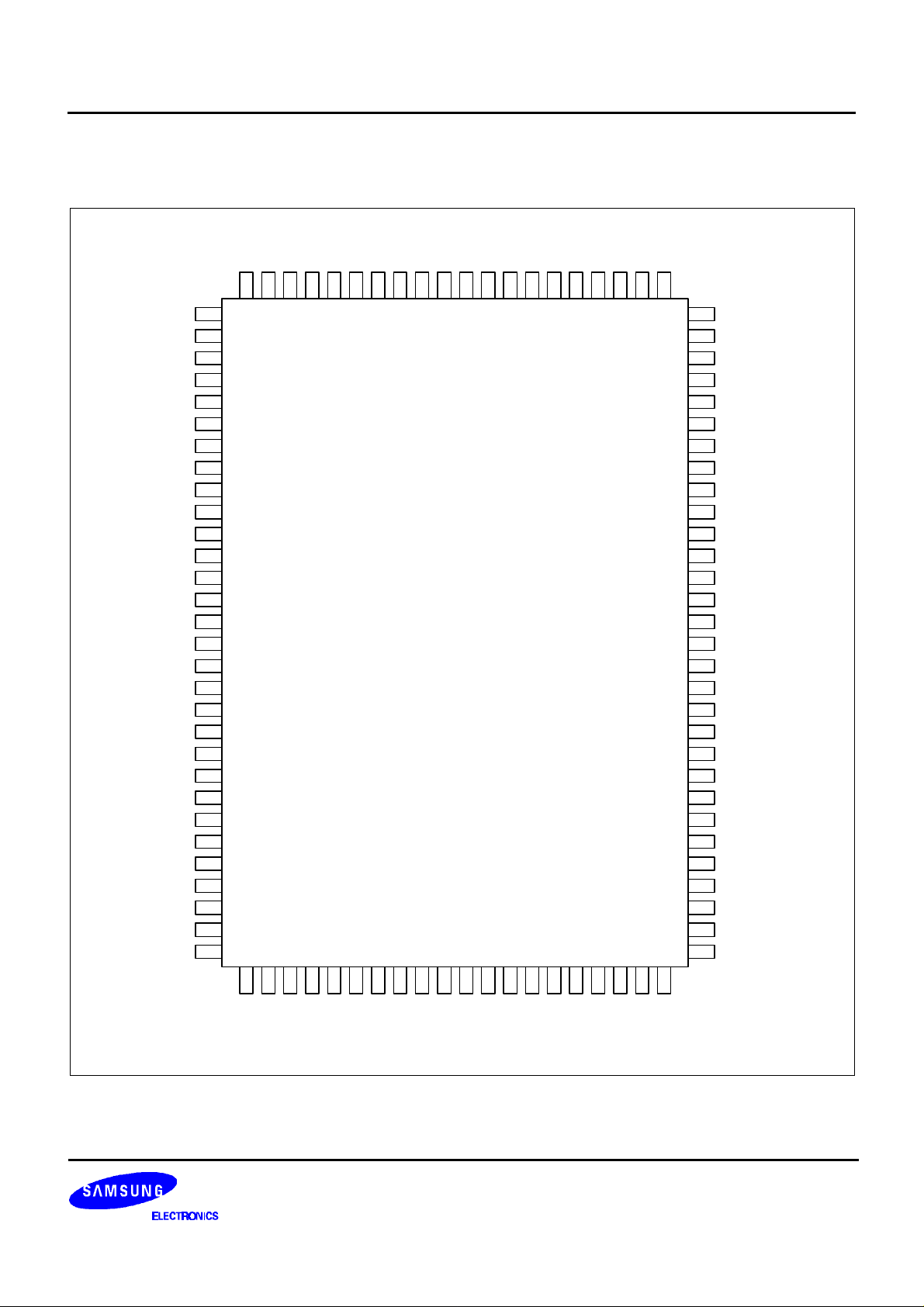
Figure 3. S5A1901H02 Pin Assignmen
44
VDD6
45
GND6
46
47
DSDO2
DBKCO2
48
49
50
DSDO1
DBCKO1
5

S5A1901H02 AUDIO EFFECT PROCESSOR
S5A1901H02 PIN DESCRIPTION
No Pin Name I/O Function Pad Type Pull Up/Down
1 ALO AO D/A analog output: left channel, 1Vrms
− −
magnitude centered around VREF
2 ARO AO D/A analog output: right channel, 1 Vrms
− −
magnitude centered around VREF
3 VSS2 AG Codec analog ground − −
4 VDD13 DP Codec digital power +5 V − −
5 GND13 DG Codec digital ground − −
6 VDD0 DP Codec digital power +5 V − −
7 GND0 DG Codec digital ground − −
8~11 NC − Reserved for chip test − −
12 VDD1 DP Digital power +5 V − −
13 GND1 DG Digital ground − −
14~17 NC − Reserved for chip test − −
18 VDD2 DP Digital power +5 V − −
19 GND2 DG Digital ground − −
20~27 NC − Reserved for chip test − −
28 VDD3 DP Digital power +5 V − −
29 GND3 DG Digital ground − −
30 SAS DI
31 HMS DI
I2C bus interface slave address selection
Host interface mode selection (0: normal, 1: I2C)
32 HCLK DI Normal host interface bit clock (max 400kHz)
33 HWEB DI Normal host interface write enable
− Down
− Down
Schmitt trigger
Schmitt trigger
Up
Up
(HWEB = 0: write, HWEB = 1: read)
34 HDATA I/O Normal host interface data In/Out
Schmitt trigger
Down
(HWEB = 0: in, HWEB = 1: out)
35 VDD4 DP Digital power +5 V − −
36 GND4 DG Digital ground − −
37 SCL DI
38 SDA I/O
I2C bus interface serial bit clock
I2C bus interface serial data in/out
Open drain −
Open drain −
39 VDD5 DP Digital power +5 V − −
40 GND5 DG Digital ground − −
6
AUDIO EFFECT PROCESSOR S5A1901H02
S5A1901H02 PIN DESCRIPTION (Continued)
No Pin Name I/O Function Pad Type Pull Up/Down
41 DSDI2 DI Digital serial data input 2 (DSDI2)
42 DBCKI2 DI DSDI2 bit clock
43 DLRCKI2 DI DSDI2 left/right flag clock
Schmitt trigger
Schmitt trigger
Schmitt trigger
44 VDD6 DP Digital power +5 V − −
45 GND6 DG Digital ground − −
46 DSDO2 DO Digital serial data output 2 (DSDO2) − −
47 DBCKO2 DO DSDO2 bit clock − −
48 DLRCKO2 DO DSDO2 left/right flag clock − −
49 DSDO1 DO Digital serial data output 1 (DSDO1) − −
50 DBCKO1 I/O DSDO1 bit clock
51 DLRCKO1 I/O DSDO1 left/right flag clock
Schmitt trigger
Schmitt trigger
Down
Down
52 VDD7 DP Digital power +5 V − −
53 GND7 DG Digital ground − −
54 DSDI1 DI Digital serial data input 1 (DSDI1)
55 DBCKI1 DI DSDI1 bit clock
56 DLRCKI1 DI DSDI1 left/right flag clock
Schmitt trigger
Schmitt trigger
Schmitt trigger
57 VDD8 DP Digital power +5 V − −
−
−
−
−
−
−
58 GND8 DG Digital ground − −
59 HACK DO Normal host interface acknowledge − −
60 TINT1 DO Interrupt indicator − −
61 NC - Reserved for chip test − −
62 SPWDN DO System power down indicator − −
63 NC - Reserved for chip test − −
64 CLKO DO Clock output 33.8688 / 3 = 11.2896MHz − −
65 VDD9 DP Digital power +5 V − −
66 GND9 DG Digital ground − −
67 XO DO Crystal oscillator output terminal (16.9344MHz) − −
68 XI DI Crystal oscillator input terminal (16.9344MHz) − −
69 CLKS DI System clock source selection (0: doubler, 1:
− Down
external)
70 MCLK I/O External clock input/doubler clock output
− Down
according to CLKS
7

S5A1901H02 AUDIO EFFECT PROCESSOR
S5A1901H02 PIN DESCRIPTION (Continued)
No Pin Name I/O Function Pad Type Pull Up/Down
71 VDD10 DP Digital power +5 V − −
72 GND10 DG Digital ground − −
73−76 NC − Reserved for chip test − −
77 GND11 DG Digital ground − −
78 VDD11 DP Digital power +5 V − −
79−84 NC − Reserved for chip test − −
85 GND12 DG Digital ground − −
86 VDD12 DP Digital power +5 V − −
87−92 NC − Reserved for chip test − −
93 RESB DI System reset (active low) − Υπ
94 VCC1 AP Codec analog power +5 V − −
95 VSS1 AG Codec analog ground − −
96 VREFI AO Codec 2.5V reference to VSS1 − −
97 VREF AO Codec 2.25V reference to VSS1 − −
98 ARI AI A/D right channel input magnitude centered
− −
around VREF should be less than or equal to 1
Vrms
99 ALI AI A/D left channel input magnitude centered
− −
around VREF should be less than or equal to 1
Vrms
100 VCC2 AP Codec analog power +5V − −
NOTES:
• DI Digital Input
• DO Digital Output
• I/O Digital Input and Output
• AI Analog Input
• AO Analog Output
• DP Digital Power
• DG Digital Ground
• AP Analog Power
• AG Analog Ground
8

AUDIO EFFECT PROCESSOR S5A1901H02
HARDWARE DESCRIPTION
DSP Core
• Up to 33 MIPS 16 bit fixed point High Performance DSP core (SSP1610)
• 16 x 16 multiplier with 32 bit product
• 32 bit ALU/accumulator
• 0.5 µm triple metal CMOS technology
Memory
• 0.5 Kword data RAM
• 6 Kword delay RAM for sound field effect
• 6 Kword program ROM
• 0.5 Kword parameter ROM for Movie Mode
Built-in A/D and D/A converters
• Stereo 16 bit Σ−∆ A/D converter
• Stereo 16 bit Σ−∆ D/A converter
Peripheral Interface
• Hardware configuration (extended to five registers using bit manipulation)
• Codec and DSIU2 interface
• DSIU1 interface
• Delay memory interface
• Parameter ROM used in Movie Mode interface
• Host interface
9

S5A1901H02 AUDIO EFFECT PROCESSOR
Extended Hardware Configuration Registers
Register Name Description
DSIU1ICR Input format control of digital source interface unit 1
DSIU1OCR Output format control of digital source interface unit 1
DSIU2ICR Input format control of digital source interface unit 2
DSIU2OCR Output format control of digital source interface unit 2/ Codec format control
CHIPCR Chip Control: DSDO1 clock source selection, Input Source Configuration Selection
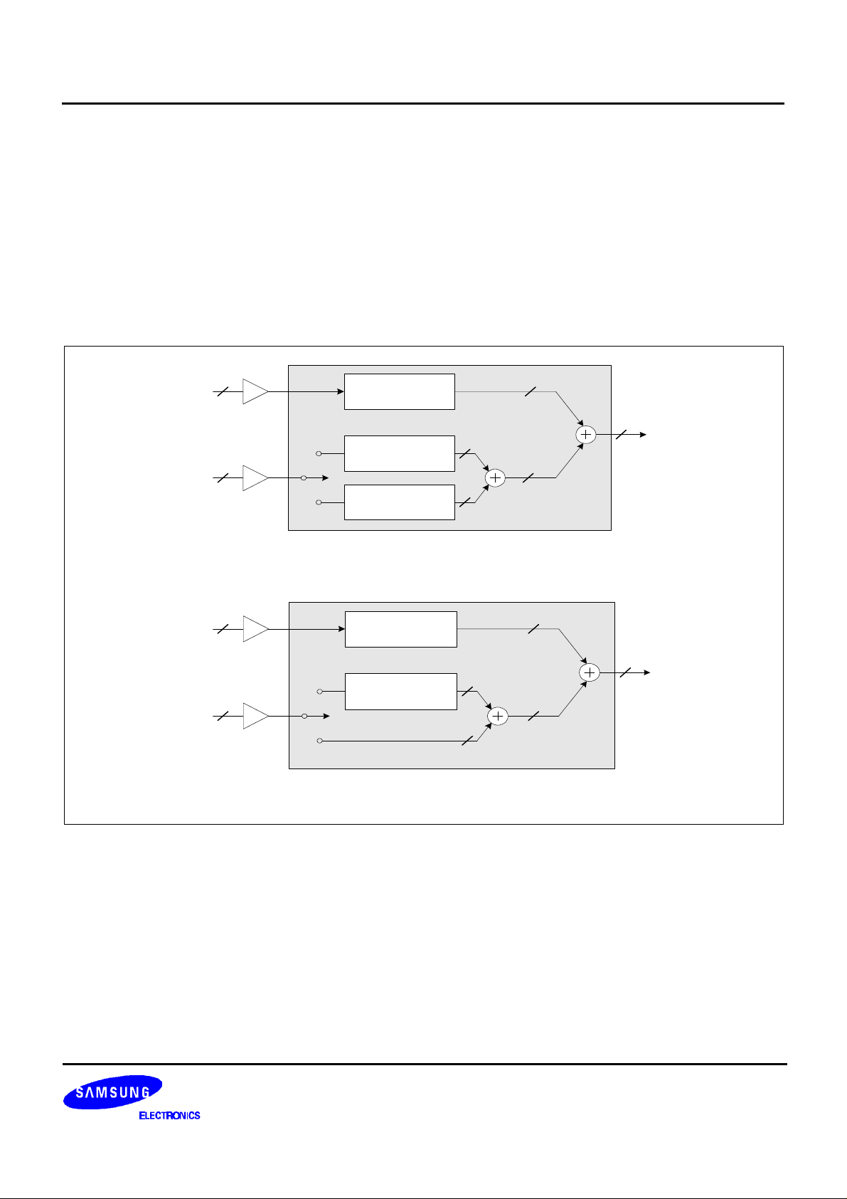
General Description of Digital Audio Interface of the S5A1901H02
The digital audio interface of the S5A1901H02 consists of 3 blocks mainly: CIU, DSIU1 and DSIU2. The CIU block
is the interface block for the built-in codec. The DSIU1 and DSIU2 blocks are for external ADC and DAC interfaces.
The DSIU2 and CIU are mutually exclusive in a sense that only one of two is working. The interface blocks can
work either slave or master mode (for DSIU1 output, both modes) depending on wether the S5A1901H02 supplies
the bit clocks and LR clocks (master), or DAC (ADC) provides the clocks (slave). For example, the DSIU1 takes the
digital audio outputsin master/32 Fs mode, which means that the S5A1901H02 (or DSIU1) provides the bit and the
LR clocks to the DAC and the audio data format 32 Fs (32 bit clocks in a LR clock period).
When an external ADC or (and) DAC is used, it is strongly recommended to use the clock, CLKO (pin #64),
provided by S5A1901H02 as the master clock for clock synchronization.
DSIU2 CIU DSIU1
slave
(support
all format*)
ADC DAC
(32Fs, 16bit)
master
(32Fs)
16 bit 16 bit
ADC DAC
master
CODEC
master
(32Fs)
S5A1901H02
slave
(support all formats*)
master & slave
(support all formats*)
ADC DAC
10
Figure 4. Digital Audio Interface Formats of the S5A1901H02

AUDIO EFFECT PROCESSOR S5A1901H02
Codec Interface
The S5A1901H02 has on chip 16 bit stereo ADC and DAC with digital filters and serial interfaces to provide CD
quality sound for audio application. The digital A/D decimation filter takes in the encoded signals from Σ−∆ A/D
modulator, and outputs 16 bit stereo digital audio data through the serial interface. The D/A interpolation filter takes
16 bit stereo audio data from the serial interface, and outputs one bit signal to the Σ−∆ D/A. The oversampling rate
of the digital filter is 128xFs, where Fs can be varied from 4kHz to 48kHz and can be changed on the fly. The serial
data interface is running at 32xFs and supports both right justified format and I2S data format. To set input and output formats of codec, see Table and Table .
Digital Source Interface Unit 1 (DSIU1)
The DSIU1 has a digital serial data input source (DSDI1) and a digital serial data output source (DSDO1). It supports 16/18/20/24 bit data length, and supports right justified, left justified or I2S format in data position. The format
of DSIU1 is controlled by a microcontroller through Host Interface Unit (HIU) and Configuration Register Unit (CRU)
as in Table 19 and Table . In formats of DSDI1 and DSDO1, only 16 bit data length is supported when the data rate
is 32xFs. The DSDO1 can operate either in slave or master mode while DSDI1 operates only in slave mode by
Configuration Register Unit (CRU) setting. Note that the MSB is transferred first.
DLRCKI1/DLRCKO1
DBCKI1/DBCKO1
RJ/16 bit/64 fs
RJ/18 bit/64 fs
RJ/20 bit/64 fs
RJ/24 bit/64 fs
LJ/16 bit/64 fs
LJ/18 bit/64 fs
LJ/20 bit/64 fs
LJ/24 bit/64 fs
IIS/16 bit/64 fs
IIS/20 bit/64 fs
IIS/18 bit/64 fs
IIS/24 bit/64 fs
L-ch R-ch
L-ch = Low, Data is synchronized with the falling edge of DBCKI1/DBCKO1
Figure 5. Data Format in DSIU1
11
S5A1901H02 AUDIO EFFECT PROCESSOR
Digital Source Interface Unit 2 (DSIU2)
The DSIU2 has a digital serial data input source (DSDI2) and a digital serial data output source (DSDO2). The
DSDI2 operates in slave mode, while the DSDO2 operates in master mode. The format of DSDI2 is same as that of
DSDI1. The format of DSDO2 is same as that of built-in codec. The format of DSDO2 supports 16 bit and 32xFs
right-justified or IIS format. The format of DSIU2 is controlled by a microcontroller through Host Interface Unit (HIU)
and Configuration Register Unit (CRU) as in Table and Table . Note that the MSB is transferred first.
DLRCKI2
DBCKI2
RJ/16 bit/64 fs
RJ/18 bit/64 fs
RJ/20 bit/64 fs
RJ/24 bit/64 fs
LJ/16 bit/64 fs
LJ/18 bit/64 fs
LJ/20 bit/64 fs
LJ/24 bit/64 fs
IIS/16 bit/64 fs
IIS/20 bit/64 fs
IIS/18 bit/64 fs
IIS/24 bit/64 fs
DLRCKO2
DBCKO2
RJ/16 bit/32 fs
IIS/16 bit/32 fs
L-ch R-ch
MSB LSBMSB LSB
MSB MSBLSB LSB
Figure 6. Data Format in DSIU2
12
AUDIO EFFECT PROCESSOR S5A1901H02
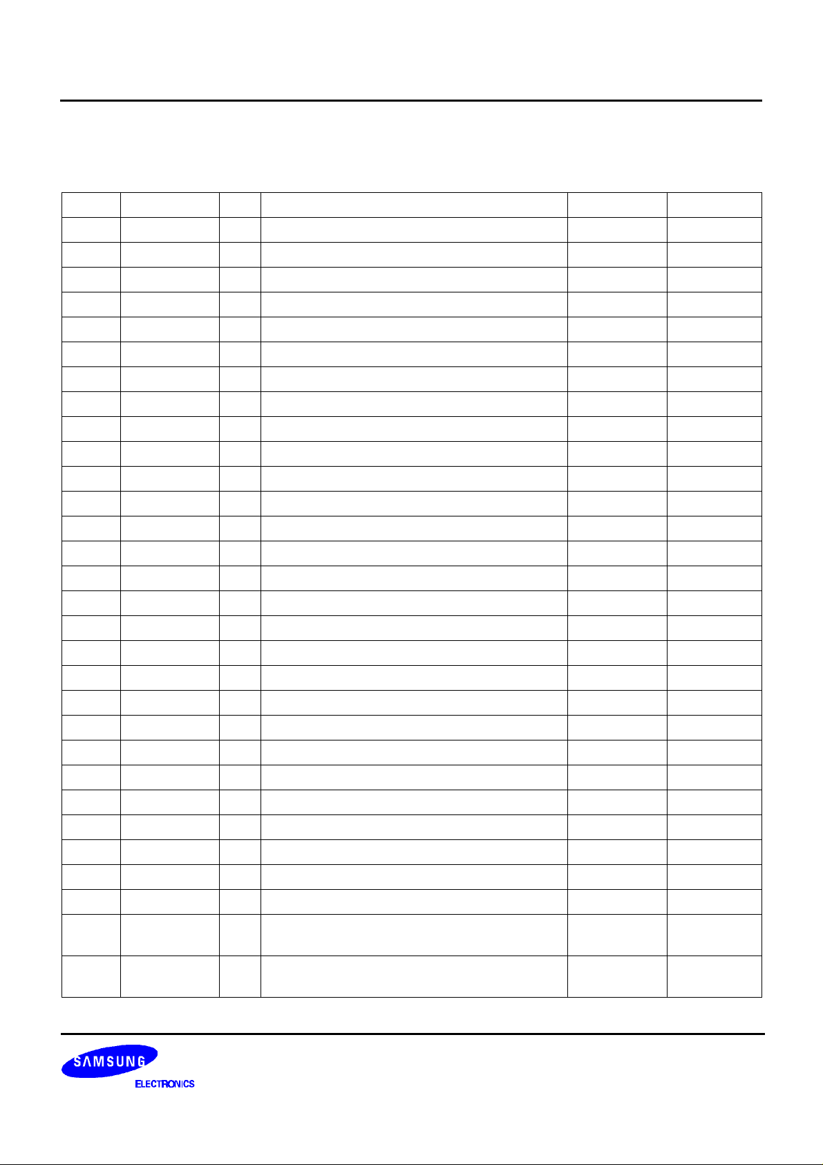
Host Interface Unit (HIU)
The S5A1901H02 receives commands and parameters in serial format from microcontroller through built-in HIU.
The data must be in byte unit (8 bit). The host commands are composed of the following three types.
• Command Only
• Command followed by Parameter
• Command followed by Parameter #1 (high byte) followed by Parameter #2 (low byte)
The details on commands used in the S5A1901H02 can be found in Chapter 4.
The HIU supports either normal microcontroller interface or I2C bus interface. In normal host interface, the related
pins are HCLK (Normal Host Interface Bit Clock), HWEB (Normal Host Interface Write Enable) and HDATA (Nor-
mal Host Interface Data In/Out). In I2C bus interface, the related pins are SDA (Serial Data Line), SCL (Serial Clock
Line) and SAS (I2C Bus Interface Programmable Slave Address Selection). One can refer to I2C Bus Specification
by Philips. The I2C bus interface in the S5A1901H02 operates in Slave-Transmitter mode. The other function of
HIU is the spectrum request function. The spectrum value is sent to microcontroller. The maximum bit clock (HCLK
or SCL) is 400kHz. Note that since the chip is being initialized for at least 1ms after reset, commands should be
transferred to the chip after 1ms.
2-Byte Operation1-Byte Operation
HWEB
HCLK
HDATA
Write Operation(Command) Write Operation(Command)
Processing Operation
MSB
From Micom
MSB
From Micom
Figure 7. Data Format in Normal Host Interface
Write Operation(Data)
Processing Operation
MSB
From Micom
13
S5A1901H02 AUDIO EFFECT PROCESSOR
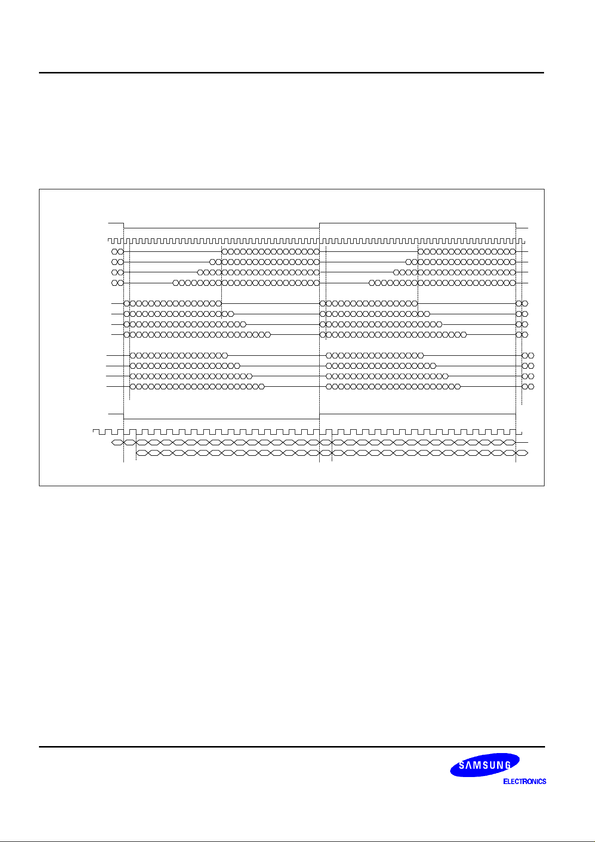
Other Write OperationSpectrum Request Operation
Write Operation Read Operation
HWEB
HCLK
HDATA
MSB
From Micom
MSB
From Chip
MSB
From Micom
Figure 8. Data Format in Normal Host Interface-Spectrum Request
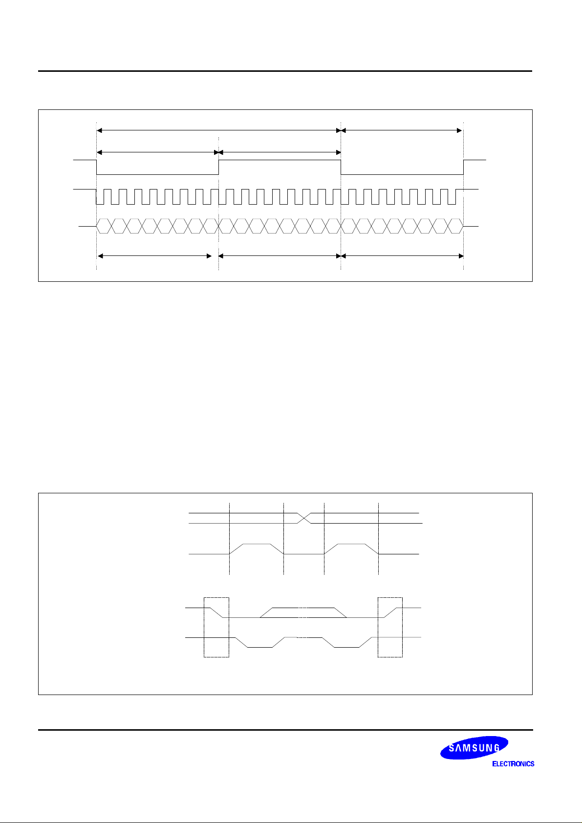
I2C Bus Interface
The S5A1901H02 can be controlled by a microcontroller via the 2-line I2C bus, SDA (Serial Data Line) and SCL
(Serial Clock Line). Both lines must be connected to a positive supply via pull-up resistor. Data transfer may be initiated only when the bus is not busy. When the bus is free, both lines are high. The data on the SDA line must be
stable during the high period of clock, SCL. When the SCL is low, the SDA can change. Every byte transferred
through the SDA line must contain 8 bits including programmable slave address and read/write direction control bit.
Each byte must be followed by acknowledge bit which is sent back to the microcontroller by the S5A1901H02 by
pulling down the SDA line. The MSB is transferred first. The setup and hold time on the SCL and SDA lines can be
found in I2C Specification by Philips.
• I2C bus interface start and stop condition
The start condition is high to low transition of the SDA line while the SCL is high. The stop condition is low to high
transition of the SDA line while SCL is high.
14
SDA
SCL
Change
of Data
Allowed
P
Stop
Condition
SDA
SCL
Data Valid
S
Start
Condition
Figure 9. Data Validity and Start/Stop Condition in I2C Bus

AUDIO EFFECT PROCESSOR S5A1901H02
• I2C Bus Interface Acknowledge
The acknowledge related clock pulse is generated by a microcontroller. The transmitter releases the SDA line
(high) during the acknowledge clock pulse. The receiver must pull down the SDA line during the acknowledge clock
pulse so that it remains stable low during the high period of this clock pulse. The slave-transmitter generates negative acknowledge when read operation processes. The negative acknowledge is generated by a master (microcontroller).
• I2C Bus Interface Slave Address Selection
Pin Name Status
Low 80 81
SAS
High 82 83
• I2C Bus Interface Specification
Chip Address Function Address DATA
MSB MSB MSB
S 1 0 0 0 0 0 A0 W A
SCL
SDA
1 0 0 0 0 0 0
Figure 10. I2C Bus Interface Format-Write Operation (SAS = 0)
LSB
Selected Slave Address (Hex)
Write Address Read Address
LSB
A
0
LSB
A
P
PS
Chip Address Function Address DATA
MSB MSB MSB
S 1 0 0 0 0 0 A0 R A
SCL
SDA
1 0 0 0 0 0 0
(S: Start Condition P: Stop Condition R: Read Operation W: Write Operation A:Acknowledge N/A: Negative Acknowledge)
LSB
LSB
A
1
Figure 11. I2C Bus Interface Format-Read Operation (SAS = 0)
LSB
N/
P
A
PS
15

S5A1901H02 AUDIO EFFECT PROCESSOR
System Clock
In the S5A1901H02, there are two ways to supply the system clock,
• Using Clock Doubler
The CLKS should be set to LOW and X-tal oscillator of 16.9344MHz is connected to XI and XO pins. Then, the
clock doubler doubles 16.9344MHz to 33.8688MHz and outputs to MCLK.
• Using External Clock Source
The CLKS should be set to HIGH. In this case, the MCLK pin is the input which is the system clock of 33.8688MHz.
Reset
The S5A1901H02 provides hardware reset and software reset. In hardware reset using RESB pin, the reset signal
has to be kept for L/R one cycle pulse width (approx. 22.67µs) for stable initialization of built-in codec. In the software reset (command code: 0x00) through HIU, system initialization is internally processed.
Power Down
The system power down mode set by host command through HIU disables all hardware macro blocks in the
S5A1901H02, i.e., DSP, delay RAM, data RAM, program ROM, glue logic and codec. Every host command can
wake-up the system power down mode.
16
AUDIO EFFECT PROCESSOR S5A1901H02
FUNCTIONAL DESCRIPTION
Bypass Mode
In bypass mode, the input is bypassed to the output with the control of volume, balance and tone.
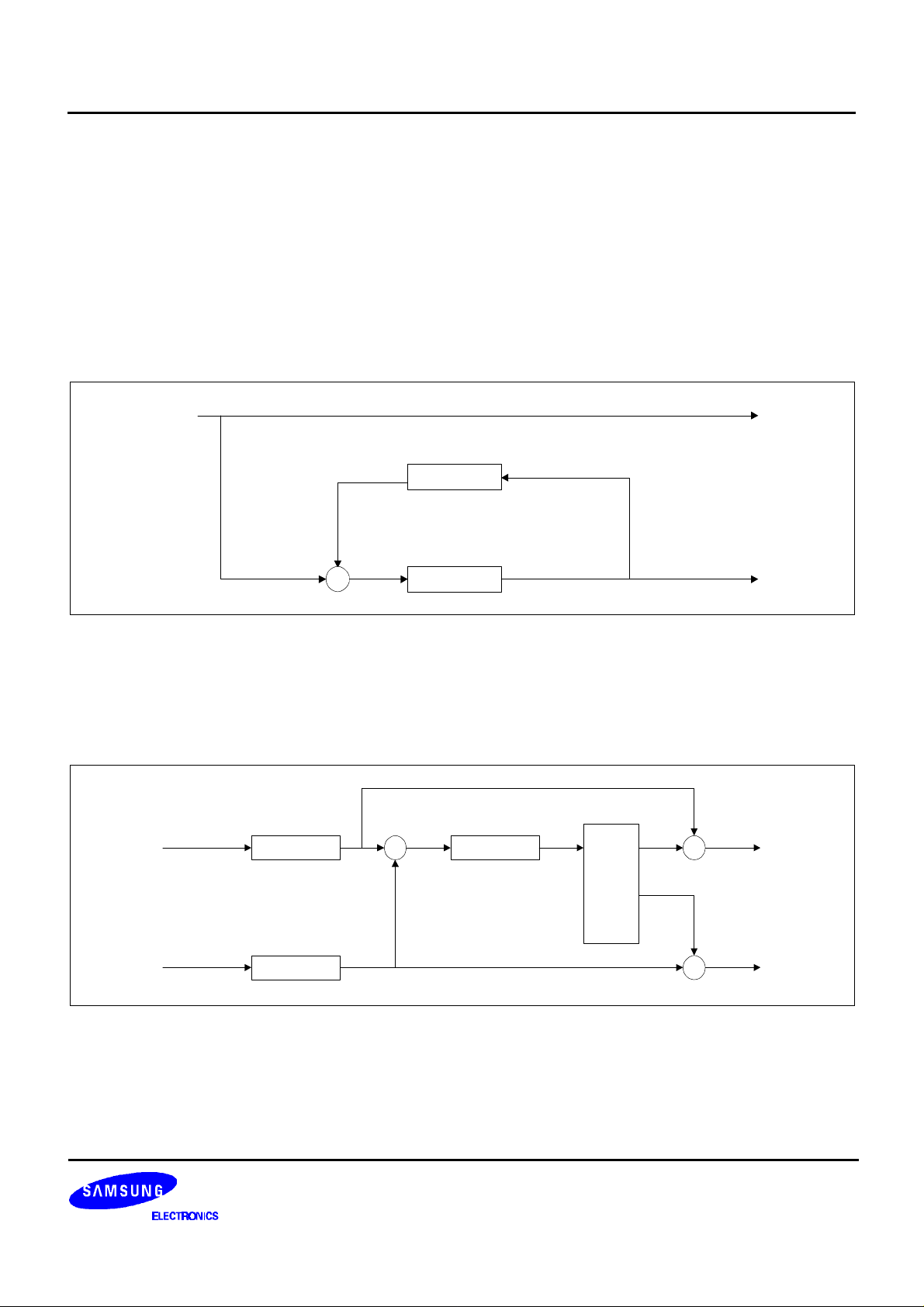
Stereo Emulation Mode I, II
These modes emulate mono input signal to stereo signal. The block diagram realizing these modes is shown in
Figure . The Stereo Emulation Mode I and II are different in the strength of effect. The Stereo Emulation Mode II
produces more stereo effect than Stereo Emulation Mode I.
Lin = Rin Lout
Delay
+
Figure 12. Block Diagram for Stereo Emulation Modes
Super Woofer Mode I, II, III
Super Woofer modes highly emphasize very low frequency component of input signal, and then, add echo effect.
The block diagram realizing these modes is shown in Figure . The Super Woofer Mode I, II and III are different in
the strength of the effect. The effect becomes stronger from Super Woofer I to Super Woofer III.
Lin Lout
Prefilter
+ Postfilter
Filter
Rout
+
Delay
Buffer
Prefilter
Figure 13. Block Diagram for Super Woofer Modes
+Rin
Rout
17

S5A1901H02 AUDIO EFFECT PROCESSOR
Hall Mode I, II and Stage Mode
Hall modes and stage mode produce effects that one feels as if he or she is in a hall or a stage respectively. The
block diagram realizing these modes is shown in Figure . The Hall Mode I and II are different in the hall size which
one can feel. The Hall Mode II produces the effect of a larger hall than that of Hall Mode I.
Lin Lout
+ Filter
+
Delay
Buffer
Rin
Figure 14. Block Diagram for Hall and Stage Modes
Arena Mode I, II
Arena modes produce effects that one feels as if he or she is in an arena. The block diagram realizing these modes
is shown in Figure . The Arena Mode I and II are different in the arena size which one can feel. The Arena Mode I
produces the effect of wider arena than that of Arena Mode II.
Lin Lout
+ Filter Delay +
Delay
+
Rout
18
Rin
Figure 15. Block Diagram for Arena Mode I, II
+
Rout
AUDIO EFFECT PROCESSOR S5A1901H02
News/Drama Mode
This mode enhances high frequency component of signal to improve the speech recognizability for news or drama
program.
Karaoke Mode I, II
The Karaoke modes receive inputs from both a microphone and an audio source. In Karaoke Mode I, the microphone input is echoed by the echo filter 1 and the audio source input is effected with the stage mode. When the
vocal canceller is selected, the audio source whose vocal component is cancelled is bypassed without stage effect.
In Karaoke Mode II, the microphone input is echoed by the echo filter 2 and the audio source input is bypassed.
Voice
Music
Voice
Music
Mic Echo I
Stage Effect
Vocal
Canceller
Karaoke Mode I
Mic Echo II
Vocal
Canceller
Karaoke Mode II
Equalizer
Equalizer
Figure 16. Karaoke Mode I, II
In Mic echo filter 1, the delay gains remain large and they are shortly decayed as time goes by. Thus, one can feel
plenty of echo while there is little aliasing between echos and original sound. The Mic echo filter 2 has a similar
structure to that of Hall mode. The effect is not stronger than that of Mic echo filter 1, but it produces a widely
spread echo which is very impressive.
19
S5A1901H02 AUDIO EFFECT PROCESSOR
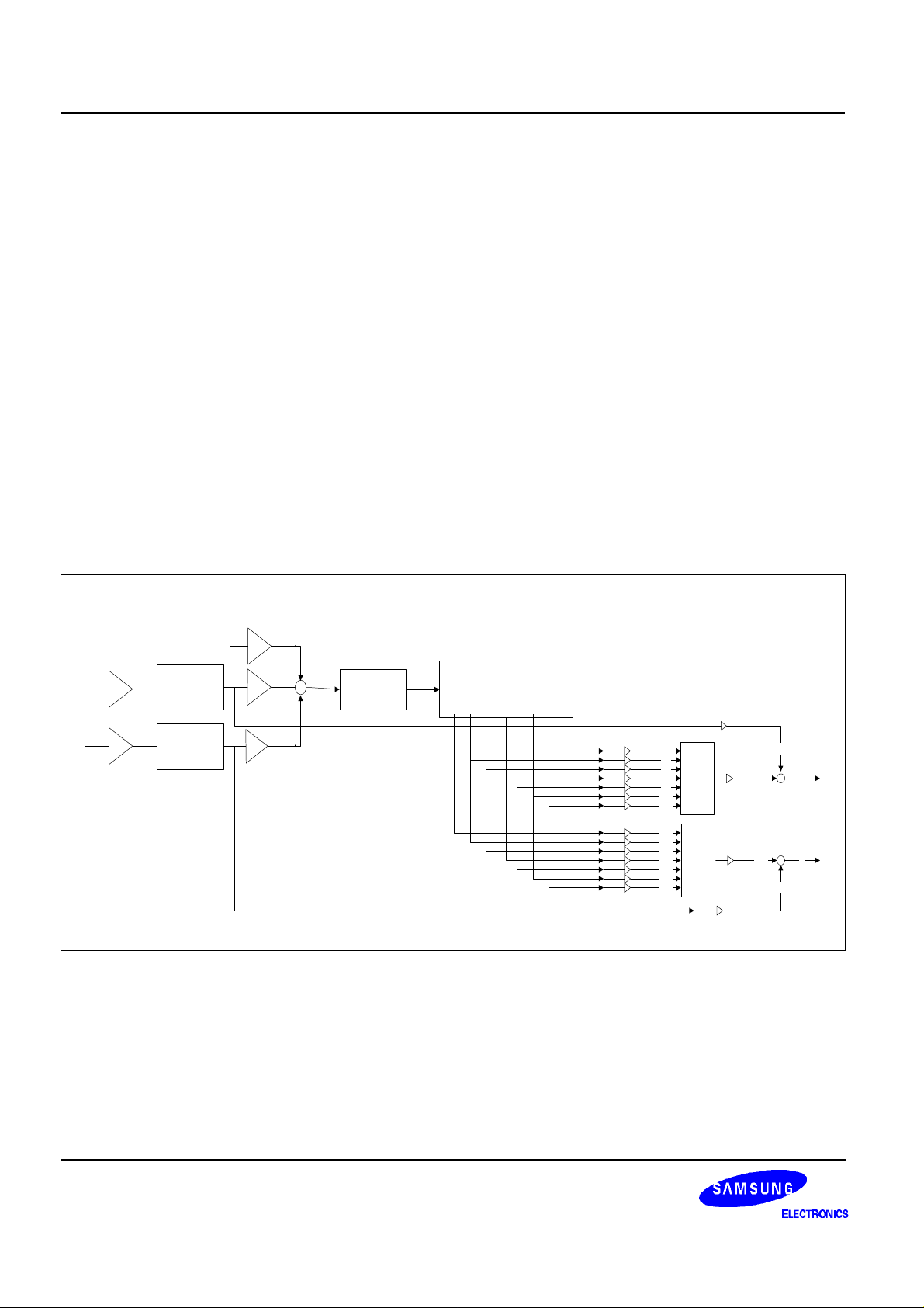
User Defined Mode
The User Defined Mode enables one to design a new sound effect mode by setting the parameters of existing filter
structure. The block diagram of this filter structure is shown in Figure . One can set these parameters by sending
host commands corresponding to each parameters. The commands used for this mode are listed in Chapter 4. The
command codes from 0x49 to 0x71 are assigned to User Defined Mode. The usage of individual parameter in Figure is as follows:
• The gain parameters, G0 and G1, are used to control left and right input gains respectively.
• The parameters, BL0, BL1 and AL1, are coefficients of the IIR filter used for left prefilter. The parameters, BR0,
BR1 and AR1, are coefficients of the IIR filter used for right prefilter. The parameters, BD0, BD1 and AD1 are
coefficients of the IIR filter used for postfilter. The structures of all three filters are realized by the first order IIR.
The zero of the transfer function of each filter is − BX1 / BX0 and the pole is − AX1, where X is L or R or D.
• The parameters, G2, G3 and G4, are left term gain, right term gain and feed-back term gain respectively.
• The parameters, G5 to G11, are gains of delayed signals in the left channel. The parameters, G14 to G20, are
gains of delayed signals in the right channel. The parameters, G12 and G21, are gains of effected output
signals. The parameters, G13 and G22, are gains of directed output signals.
• The parameter, T0, is the pointer address of the feed-back signal in the delay memory. The parameter, Tc, is
the pointer address of the current input signal. The parameters, T1 to T7, are pointers designating addresses of
the 7 different delayed signals. Note that the pointer address is same as the amount of delay. Thus, T0 to T7
values can be simply determined as the amount of delay which one wants to set.
G4
BL0
G0
BL1
BR0
G1
BR1
AL1
Left Prefilter
AR1
Right Prefilter
G2
G3
BD0
+
BD1
AD0
Postfilter Delay Line Buffer
T
c
T1T2T3T4T5T6T
T
0
7
G21
G13
G22
++G12
L
R
G5
G6
G7
G8
G9
G10
G11
G14
G15
G16
G17
G18
G19
G20
+
+
Figure 17. Block Diagram for User Defined Mode
20

AUDIO EFFECT PROCESSOR S5A1901H02
Movie Mode I, II
The Movie Mode I and II create 3-dimensional sound images from 2-channel stereo input signals. The Movie ModeI enhances stereo images dynamically using the Samsung proprietary TLA (Table Lookup Algorithm) method. One
perceives as if he or she is in the live stage. The Movie Mode II uses a sound source relocalization technique based
on Head Related Transfer Function (HRTF). Only using two front speakers, one can perceive as sound coming
from various directions.
Graphic Equalizer
The S5A1901H02 provides the graphic equalizer having following features.
• 3/5/7-band graphic equalizer
• 5/7-band spectrum analyzer display
• ± 12dB adjustable range
The 3-band graphic equalizer can be used as a simple digital tone control (as bass and treble control).
Center Frequencies of Equalizer Bands (Hz)
Band 3-Band Mode 5-Band Mode 7-Band Mode
Band0 63 100 63
Band1 1 K 300 160
Band2 16 K 1 K 400
Band3 − 3 K 1 K
Band4 − 10 K 2.5 K
Band5 − − 6.4 K
Band6 − − 16 K
The gain control of each band uses an attenuation table containing attenuation values, which has the size of 25 to
implement ±12dB with 1dB step control
21
 Loading...