

Page 1
Global LCD Panel Exchange Center
G
G
G
mvyGtlzzyza
GGGGGGGGGGGGGGGGGGGGGGGGGGGGGGGGGGGGGGGGGGGGGGGkh{laGq|sGX[SGYWXWG
www.panelook.com
TOP
CUSTOMER’S SPECIFICATIONS
106.68cm (42 Inch) Wide Plasma Display Module
MODEL:S42AX-YD13(M3)
(NTSC/PAL)
* This specification will be approved by both TOP and Samsung SDI Co.,Ltd.
* Please return one of this specification with your signature for approval.
Proposed by: Approved by:
Signature
Signature
G/Manager. ChangSub, Son
PDP Development Team, PDP Business
Division, Samsung SDI Co., Ltd
One step solution for LCD / PDP / OLED panel application: Datasheet, inventory and accessory!
www.panelook.com
Page 2

Global LCD Panel Exchange Center
SAMSUNG SDI Corporation Plasma Display Panel
www.panelook.com
Revision History
No Date Description Of Changes Rev. no Approval
1 DEC 22, 09 Tentetive SPEC for customer application R0.0
1)30% L/R :
2 JAN 12, 10
z Typical 190cd/້ -> 165cd/້
z Minimum 160 cd/້ -> 155 cd/້
Page 7
SAMSUNG SDI - 2/64 - Rev.01 31/12/0
One step solution for LCD / PDP / OLED panel application: Datasheet, inventory and accessory!
www.panelook.com
Page 3

Global LCD Panel Exchange Center
㡺⮮
㺛Ṟ䞒Ṗ 㩫㦮♮㠊 㧞㰖 㞠㔋┞┺
㡺⮮! 㺛Ṟ䞒Ṗ 㩫㦮♮㠊 㧞㰖 㞠㔋┞┺
㡺⮮! 㺛Ṟ䞒Ṗ 㩫㦮♮㠊 㧞㰖 㞠㔋┞┺
㡺⮮! 㺛Ṟ䞒Ṗ 㩫㦮♮㠊 㧞㰖 㞠㔋┞┺
㡺⮮! 㺛Ṟ䞒Ṗ 㩫㦮♮㠊 㧞㰖 㞠㔋┞┺
㡺⮮! 㺛Ṟ䞒Ṗ 㩫㦮♮㠊 㧞㰖 㞠㔋┞┺
㡺⮮! 㺛Ṟ䞒Ṗ 㩫㦮♮㠊 㧞㰖 㞠㔋┞┺
㡺⮮! 㺛Ṟ䞒Ṗ 㩫㦮♮㠊 㧞㰖 㞠㔋┞┺
www.panelook.com
SAMSUNG SDI Corporation Plasma Display Panel
TABLE OF CONTENTS
TU1. DESCRIPTIONUT ......................................................................................................................... 5
TU2. FEATURESUT ............................................................................................................................... 5
TU3. PRODUCT NAME AND MODEL NUMBERUT ....................................................................... 5
TU4. FUNCTION OUTLINEUT ............................................................................................................ 5
TU5. BLOCK DIAGRAMUT ................................................................................................................. 6
TU6. DISPLAY CHARACTERISTICSUT ........................................................................................... 7
TU6.1 DISPLAY PERFORMANCEUT ........................................................................................................ 7
TU6.2 DISPLAY CELL ARRANGEMENTUT .............................................................................................. 8
TU6.3 LUMINANCE MEASUREMENT CONDITIONUT............................................................................... 9
TU6.4 CONTRAST MEASUREMENT CONDITIONUT ............................................................................... 10
TU6.5 DISPLAY CELL DEFECT SPECIFICATIONUT ............................................................................... 11
TU6.6 UNIFORMITY SPECIFICATIONSUT .............................................................................................. 12
TU6.7 POWER CONSUMPTIONUT.......................................................................................................... 13
TU6.8 GAMMA CHARACTERISTICSUT .................................................................................................. 17T
TU
6.9 FILM FILTERUT ......................................................................................................................... 19
TU6.10 WHITE BLANCEUT.................................................................................................................. 21
TU7. SOUND PRESSURE LEVEL SPECIFICATIONUT .............................................................. 19
TU7.1 MEASURING CONDITIONUT ...................................................................................................... 22
TU7.2 SOUND PRESSURE LEVELUT ..................................................................................................... 22
TU8. MECHANICAL CHARACTERISTICSUT............................................................................... 23
TU8.1 MECHANICAL SPECIFICATIONSUT ............................................................................................ 23
TU8.2 MECHANICAL CHARACTERISTICSUT......................................................................................... 23
TU9. ENVIRONMENTAL CONDITIONSUT ................................................................................... 24
TU9.1 OPERATIONAL ENVIRONMENTAL CONDITIONUT ...................................................................... 24
TU9.2 STORAGE ENVIRONMENTAL CONDITION *1UT ......................................................................... 24
TU9.3 PANEL SURFACE CONDITIONUT ............................................................................................... 25
TU10. INTERFACE SIGNAL SPECIFICATIONSUT...................................................................... 26
TU10.1 CONFIGURATION CONTEXTUT ................................................................................................ 26
TU10.2 INTERFACE FUNCTION SPECIFICATIONS (INPUT DATA AND DISPLAY PROCESSING)UT ........
.
TU10.3 INPUT SIGNAL DEFINITIONUT ...............................
TU10.4 LVDS SIGNAL DEFINITION AND FUNCTIONUT .....
TU10.5 LVDS SIGNAL PIN ASSIGNMENTUT .....................
TU10.6 VIDEO SIGNAL DEFINITION AND FUNCTIONUT ....................................................................... 30
TU10.7 ELECTRICAL CONDITION OF INTERFACE SIGNALUT
TU10.8 VIDEO SIGNAL INTERFACE TIMING CONDITIONSUT
TU10.9 LVDS INTERFACE TIMING CONDITIONSUT ..........
TU10.10 LVDS CONNECTION SPECIFICATIONSUT ............
SAMSUNG SDI - 3/64 - Rev.01 31/12/0
!
.
.
.
.
.
.
.
One step solution for LCD / PDP / OLED panel application: Datasheet, inventory and accessory!
www.panelook.com
Page 4

Global LCD Panel Exchange Center
㡺⮮! 㺛Ṟ䞒Ṗ 㩫㦮♮㠊 㧞㰖 㞠㔋┞┺
www.panelook.com
SAMSUNG SDI Corporation Plasma Display Panel
TU10.11 I2C INTERFACE CONDITIONSUT..........................
TU11.ADDRESS MAPUT ................................................... 㡺⮮! 㺛Ṟ䞒Ṗ 㩫㦮♮㠊 㧞㰖 㞠㔋┞┺.
TU12.UT TUPOWER SUPPLY UNIT SPECIFICATIONUT ..................................................................... 42
TU12.1UT TUINPUT REQUIREMENTSUT ................................................................................................... 42
TU12.2 TUELECTRICAL CHARACTERISTIC OVERVIEWUT .................................................................... 43UT
TU
12.3 TUOUT DIMENSION FOR REFERENCEUT .................................................................................. 43UT
12.4 TUPOWER APPLYING SEQUENCEUT ........................................................................................ 44UT
TU
12.6 TUMECHANICAL OUT DRAWINGUT ........................................................................................ 46UT
TU
TU
13. MECHANICAL DIMENSION DRAWINGUT....................................................................... 49
TU13.1 FRONT SIDEUT........................................................................................................................ 49
TU13.2 REAR SIDEUT ......................................................................................................................... 49
TU13.2 REAR SIDEUT ......................................................................................................................... 50
TU14. LABELUT ................................................................................................................................... 51
TU14.1 LABEL TYPEUT ....................................................................................................................... 51
TU14.2 LABEL LOCATIONUT ............................................................................................................... 52
TU15. PACKINGUT.............................................................................................................................. 53
TU15.1 PACKING DIMENSION AND PARTS LISTUT .............................................................................. 53
TU15.2 PACKING ASSEMBLY DRAWINGUT ......................................................................................... 53
.
TU16. RELIABLITYUT ....................................................................................................................... 54
TU16.1 EXPECTED SERVICE LIFEUT ................................................................................................... 54
TU16.1.1DefinitionUT .................................................................................................................... 54
TU16.1.2 Test condition and life timeUT........................................................................................ 54
TU16.2 DISCLAIMERUT ...................................................................................................................... 54
TU16.4 CERTIFICATEUT ...................................................................................................................... 54
TU17. WARNING CAUTION / NOTICEUT..................................................................................... 55
TU17.1 WARNINGUT........................................................................................................................... 55
TU17.2 CAUTIONUT ............................................................................................................................ 57
TU17.3 NOTICEUT............................................................................................................................... 58
SAMSUNG SDI - 4/64 - Rev.01 31/12/0
One step solution for LCD / PDP / OLED panel application: Datasheet, inventory and accessory!
www.panelook.com
Page 5

Global LCD Panel Exchange Center
SAMSUNG SDI Corporation Plasma Display Panel
www.panelook.com
1. DESCRIPTION
The S42AX-YB09(M1) and S42AX-YD13 are a 42-inch wide full color plasma display
Module with a resolution of 1024(H) Ý 768(V) pixels. The display module includes the
Plasma Display Panel, the Panel Driving Electronics, the Logic Control Board.
2. FEATURES
x Wide aspect ratio(16:9) 42 inch diagonal display screen. The display area is 933.89mm
wide and 532.22mm high.
x Slim and light weight. The display Module is 45.2mm in depth and weight only
approx. 11.9kg.
x 1073.7 million colors(10Bit), or 16.77 million colors(8Bit) combination of R,G and B
digital data.(According to LVDS input selection)
x High Luminance, High contrast, Wide viewing angle. The screen has a white peak
Luminance of typical 500 cd
contrast of typical 10,000:1(NTSC/PAL).
And a viewing angle of greater than 160¶ comparable to that achieved
/້(In Film transmissivity 45.0%, NTSC/PAL),
3. PRODUCT NAME AND MODEL NUMBER
x Product name : 42 inch Full Color Plasma Display Module
(abbreviation : PDP Module)
x Model number : S42AX-YD13(M3) (Project name : U2P)
4. FUNCTION OUTLINE
x The plasma display module has an APC(Automatic Power Control) function which
restricts power consumption within the certain value with regard to each display load
ratio.
x The plasma display module is operated by following digital video signals; Vertical
synchronous signal, Horizontal synchronous signal, Enable signal and 8~12bit data
signals of each R, G and B color. All signals are based on LVDS level.
x The plasma display module is operated at 50Hz60Hz frame rate. An external frame rate
conversion is required in order to display the other formats.
x The plasma display module requires several types of input power voltages ; voltage for
logic IC, voltage for Gate Driver, voltage for Sustain and voltage for Address.
x The plasma display module is operated at progressive signal only.
An external progressive scan conversion is required in order to display the other formats.
SAMSUNG SDI - 5/64 - Rev.01 31/12/0
One step solution for LCD / PDP / OLED panel application: Datasheet, inventory and accessory!
www.panelook.com
Page 6

Global LCD Panel Exchange Center
www.panelook.com
SAMSUNG SDI Corporation Plasma Display Panel
5. BLOCK DIAGRAM
LVDS SIGNAL
ULOGIC CONTROLLERU
LVDS I/F CONTROLLER
DATA PROCESSOR
DISPLAY DATA
U U
SCAN PULSE
DRIVER
PDP
1024Ý768 Pixels
DATA DRIVER
DRIVING VOLTAGE
SUSTAIN PULSE
DRIVER
POWER SUPPLY UNIT
Figure-1. Block Diagram of PDP module
SAMSUNG SDI - 6/64 - Rev.01 31/12/0
One step solution for LCD / PDP / OLED panel application: Datasheet, inventory and accessory!
www.panelook.com
Page 7
Global LCD Panel Exchange Center
www.panelook.com
SAMSUNG SDI Corporation Plasma Display Panel
6. DISPLAY CHARACTERISTICS
6.1 Display Performance
No Item Rating
1 Display Pixels
Horizontal 1024 ൴Vertical 768 pixels
(1 pixel = 1 R,G,B cells)
2 Display Cells Horizontal 3,072 ൴Vertical 768 cells
3 Pixel Pitch
Horizontal 912༁൴Vertical 693༁
R Horizontal 304༁൴Vertical 693༁
4 Cell Size
G Horizontal 304༁൴Vertical 693༁
B Horizontal 304༁൴Vertical 693༁
5 Pixel Type R, G, B Non stripe (refer to Figure-2)
6
Effective Display
Size
7 Number of color
Peak Luminance *1
8
(peak algorithm on)
Horizontal 933.89༂൴Vertical 532.22༂
[ 36.77 inch ൴ 20.95 inch ]
1073.7 million colors (10Bit)
16.77 million colors ( 8Bit)
Typical 500 cd/້ , Minimum 400 cd/້
Contrast Ratio *2
9
10
(in dark room,
peak algorithm on)
Brightness
(Full white Brightness)
1,000,000:1
Typical 60cd/້ , Minimum 50 cd/້
* 30% L/R : Typical 165cd/້ , Minimum 155 cd/້
11 Viewing Angle *3 Over 160
(Note)
* 1. Luminance and Color Coordinates are the values that were measured with Full load
ratio white pattern. The condition for measurement is shown in Figure-3.
* 2. Contrast Ratio is calculated from the display Luminance and the non-display
Luminance value. Display condition is shown in Figure-4.
* 3. Viewing angle is a critical angle at which the Luminance is reduced to 50% to the
Luminance perpendicular to the PDP Module. The Luminance is measured by a noncontact luminance meter MINOLTA CA-100Plus.
SAMSUNG SDI - 7/64 - Rev.01 31/12/0
One step solution for LCD / PDP / OLED panel application: Datasheet, inventory and accessory!
www.panelook.com
Page 8

Global LCD Panel Exchange Center
www.panelook.com
SAMSUNG SDI Corporation Plasma Display Panel
6.2 Display Cell Arrangement
1st
Pixel
Row
2nd
Pixel
Row
767th
Pixel
Row
1st
Pixel
Column
Pixel Pitch (Width): 0.912 mm
Pixel
Pitch
2nd
Pixel
Column
ڭڢڝ ڭڢڝ ڭڢڝ
ڭڢڝ ڭڢڝ ڭڢڝ
WUZ W[G
WUZW[G
WUZ W[G
ڭڢڝ ڭڢڝ ڭڢڝ
3rd
Pixel
Column
ڞۀۇۇ
ګۄۏھۃ ڣۀۄۂۃۏ
ڃڋډڑڔڎ ۈۈڄ
1022th 1023th 1024th
Pixel Pixel Pixel
Column Column
ڭڢڝ ڭڢڝ ڭڢڝ
ڭڢڝ ڭڢڝ ڭڢڝ
ڭڢڝ ڭڢڝ ڭڢڝ
Column
768th
Pixel
Row
ڭڢڝ ڭڢڝ ڭڢڝ
Figure-2.Display Cell Arrangement
ڭڢڝ ڭڢڝ ڭڢڝ
SAMSUNG SDI - 8/64 - Rev.01 31/12/0
One step solution for LCD / PDP / OLED panel application: Datasheet, inventory and accessory!
www.panelook.com
Page 9

Global LCD Panel Exchange Center
g
www.panelook.com
SAMSUNG SDI Corporation Plasma Display Panel
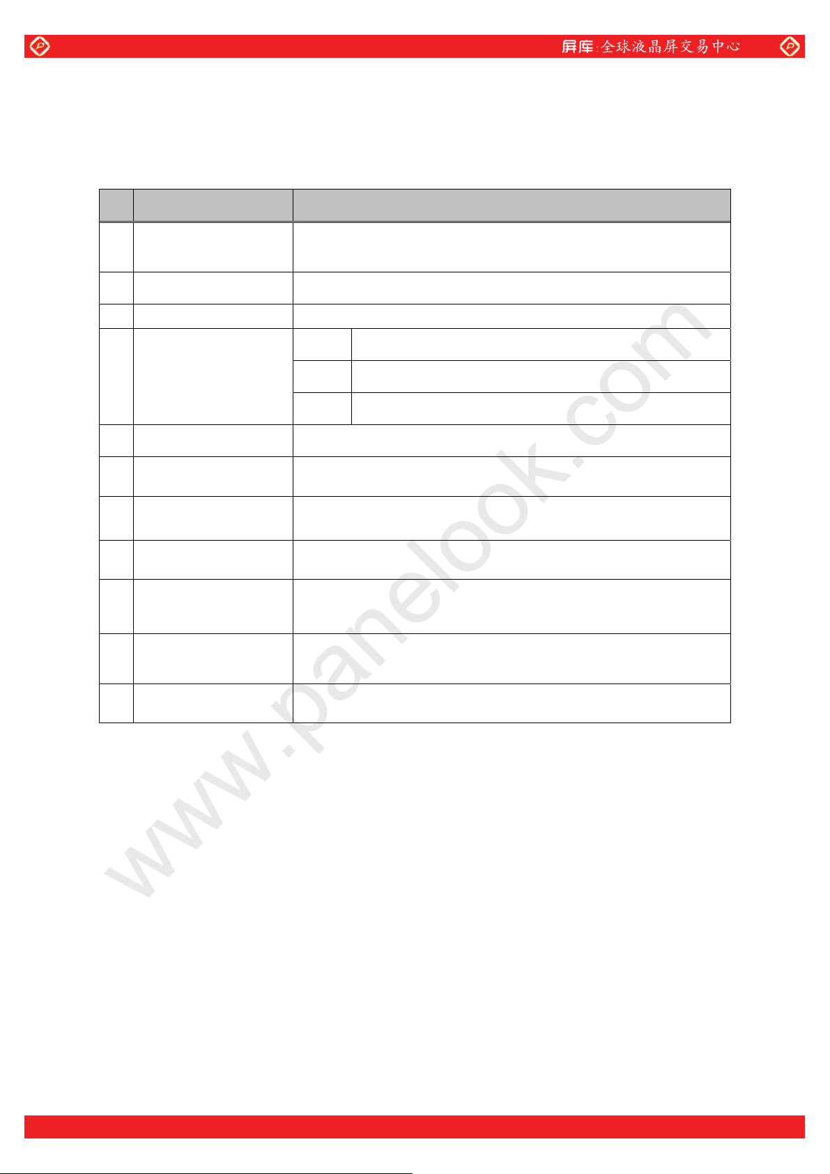
6.3 Luminance Measurement Condition
(1) Display Pattern
Effective Display Area
Effective Dis play Area
460 104 460
Unit : Pixels(=lines)
marked area : White display area by maximum gradation setting
marked area : Black color (non-dis play area)
ure-3. DisplayPattern forBrightness & Contrast Ratio Measurement
Fi
345
78
345
(2) Display Area ratio : 1% white window
(3) Vsync : 16.7ms
(4) Measuring equipment : MINOLTA CA-100Plus
Pattern Generator(VG-828, LVDS Output).
(5) Ambient Temperature : Room Temperature
(6) Ambient Luminance : Dark Room (<2 lux)
[ Note]
1. Measurement is done within 30 seconds after Power On. The temperature of panel
before measurement is room temperature (25ଇ).
2. Measurement is done within 3 seconds after Display Pattern(
mTZPGvG
SAMSUNG SDI - 9/64 - Rev.01 31/12/0
One step solution for LCD / PDP / OLED panel application: Datasheet, inventory and accessory!
www.panelook.com
Page 10
Global LCD Panel Exchange Center
www.panelook.com
SAMSUNG SDI Corporation Plasma Display Panel
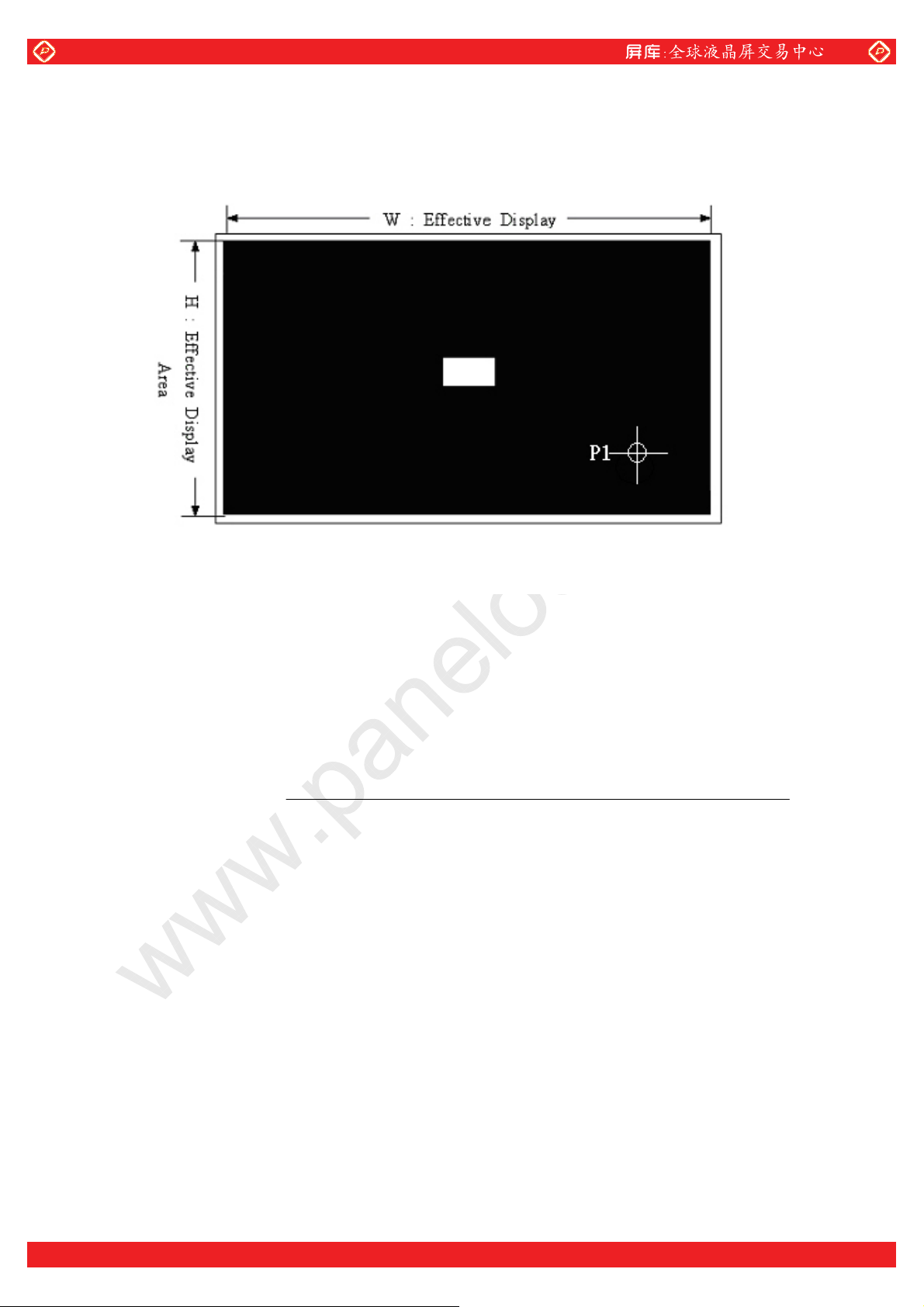
6.4 Contrast Measurement Condition
(1) Measuring point
Figure-4. Measurement point
(2) Vsync : 16.7 ms
(3) Measuring Equipment : MINOLTA CA-100Plus
Pattern Generator(VG-828, LVDS Output).
(4) Contrast Calculation formula
Luminance of 1% white window Area at the center of the screen
Contrast ratio =
Luminance of Black Area *1
ૺ Note ૻ
1. For mass production test purposes, it is recommended to measure just 1 point, P1 of
Figure 4 on display pattern of Figure 3.
2. Measuring point _P1 is that minimum luminance point from among effective display
area
(5) Ambient Light : Dark Room (<2 lux)
SAMSUNG SDI - 10/64 - Rev.01 31/12/0
One step solution for LCD / PDP / OLED panel application: Datasheet, inventory and accessory!
www.panelook.com
Page 11
Global LCD Panel Exchange Center
~G
oV[G
GiG
GhG
oV[G
oVYG
oG
~V[G ~VYG ~V[G
www.panelook.com
SAMSUNG SDI Corporation Plasma Display Panel
6.5 Display Cell Defect Specification
In some cases, a panel may have defective cells that cannot be controlled.
These defective cells can be categorized into three types;
(1) Non-lighting cell defect : defect in which the cell is always off
(2) Non-extinguishing cell defect : defect in which the cell is always on.
(3) Flickering cell defect : defect in which the cell is flickering.
(4) High intensity cell defect : defect in which the cell is brighter than other cells
(5) Test Pattern : Full White, Full Red, Full Green and Full Blue with 1024 gray level.
The display cell defect specifications define the allowed limits for display cell defects
and
are used as the criteria in determining whether a panel should be shipped.
Item
Non-lighting cell 3 and less 10 and less
Non-extinguishing cell 1 and less 2 and less
Flickering cell
(the W/R/G/B screen)
Flickering cell
(the other pattern)
High Intensity Cell 1 and less 2 and less
Figure-5. Measurement Area
Number of cell defects
A Zone B Zone
2 and less 3 and less
1 and less 2 and less
Remark
Regardless of A and B Zone,
Maximum 1 Cell Defect
in an area of 20*20mm
is allowed.
Continuous Cell 1 and less 2 and less
Total defect 14 and less
SAMSUNG SDI - 11/64 - Rev.01 31/12/0
One step solution for LCD / PDP / OLED panel application: Datasheet, inventory and accessory!
www.panelook.com
Page 12

Global LCD Panel Exchange Center
x
x
www.panelook.com
SAMSUNG SDI Corporation Plasma Display Panel
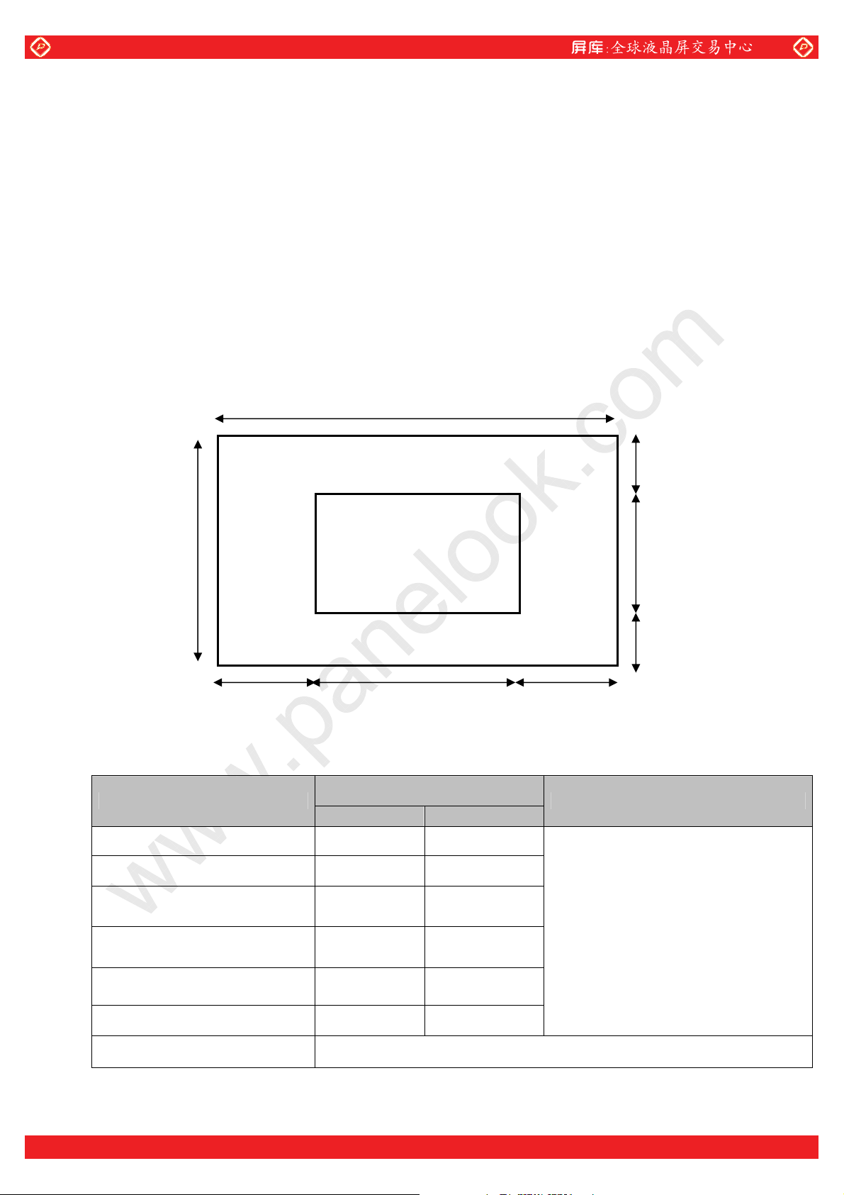
6.6 Uniformity Specifications
The color-PDP uses ultraviolet light produced by gas discharge to illuminate phosphor.
Uneven phosphor coating and inconsistent discharge characteristics cause slight difference
in brightness among the sections in a panel.
Item
Full white
brightness
variation
Equation
Definition
The brightness is measured at 9 points (A1~A9 of
Fig-6) on full white pattern.
The full white brightness variation as then calculated
from the following equations.
Max x
x Min
u 100%
Specification
15% and less
u 100%
&
The brightness variation specifications define the allowed limits for brightness differences
and the criteria in determining whether a panel is shipped.
W : Effective Display Area
H : Effective Display Area
A1 A2 A3
A4
A7
W*0.1 W*0.1
Figure-6. Measuringareas
A5 A6
A8 A9
H* 0.1
H* 0.1
SAMSUNG SDI - 12/64 - Rev.01 31/12/0
One step solution for LCD / PDP / OLED panel application: Datasheet, inventory and accessory!
www.panelook.com
Page 13

Global LCD Panel Exchange Center
(
www.panelook.com
SAMSUNG SDI Corporation Plasma Display Panel
6.7 Power consumption
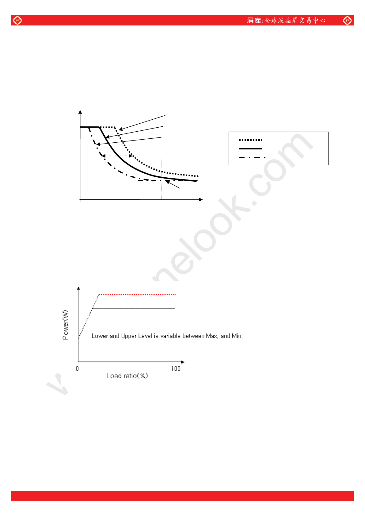
6.7.1 APC (Automatic Power Control) Function
The PDP has an APC (Automatic Power Control) function for the panel driver power source.
When the total display load ratio exceeds approximately 10%, total power consumption is
limited within a specified level (=Lower Power Limit) by APC function.
The operation behavior of APC function is called as SLOW-APC. When the display loadratio changes from low to high value, the power-consumption rises instantly to “Upper
Power Limit” and gradually decreases until it reaches to the “Lower Power Limit.”
[Note] Number of steps may Power vary as a function of the load ratio.
Power
Upper Power
Limit
Power
Load-ratio
Time for transition between 2 setps = 8 frames
Lower Power
Limit
This could be controlled by R HOLD TIME)
t
Figure 7. Slow APC Behavior
6.7.2 Brightness and Power Mode Control
This PDP module offsers two methods for Brightness and Power mode control.
One is APCO(APC Offset) for Peak-Brightness control, and the others are PUG and
PLG
for power mode control. APCO, PUG and PLG are registers controllable through I2C
communication from image B’d. For a detailed address and data bits of these registers ,
refer to the Chapter 11. Address Map.
(1) Peak-Brightness Control( APCO)
- controls the max.sustain number
- APCO variable range : 0010h~01FFh (cf. 00C8h~01F4h @3D Mode)
Sustain
number
Max. Sustain
Normal Bright Mode (APCO=0000h)
2/3 Peak-bright Mode (APCO=00F0h)
1/3 Peak-bright Mode (APCO=1A4h)
Min. Sustain
SAMSUNG SDI
0
C
max
One step solution for LCD / PDP / OLED panel application: Datasheet, inventory and accessory!
load ratio
- 13/64 100%
Figure-8. APCO Behavior
www.panelook.com
Page 14
Global LCD Panel Exchange Center
@
)
N
r
www.panelook.com
SAMSUNG SDI Corporation Plasma Display Panel
(2) ASLG ( Power-Mode Control using ASL gain function)
- ASLG variable range : 80~FFh
- Maximum available power decrease by increasing ASLG above 80h(NTSC)
Sustain
number
Max. Sustain
Min. Sustain
ASLG < ASLG’
ASLG’ = 60h
ASLG > ASLG’
load at F/W pattern
NTSC(50h@PAL
High-Power Mode
Powe
Saturated at Min. Sustain
0
Load-ratio
100%
-
(3) Power-Mode Control (PLG)
- PLG(Power Lower Gain control register)
- Variable range : 00h ~ FFh(Tentative) , Default Value : 80h
- PLG is for lower power level.
- PLG value : smaller than the default in order to make less power consumption.
ormal Mode
-Save Mode
Max(Guarantee Stress) : 215W
Typical : 175W
Figure-10. APCL Behavior(PLG Adjust)
SAMSUNG SDI - 14/64 - Rev.01 31/12/0
One step solution for LCD / PDP / OLED panel application: Datasheet, inventory and accessory!
www.panelook.com
Page 15

Global LCD Panel Exchange Center
www.panelook.com
SAMSUNG SDI Corporation Plasma Display Panel
(4)Power- Consumption Ratio( BY ASLG, PLG)
PLG ASLG ASLG_SW Power- Consumption Ratio
80 128 80 128 OFF 100%
70 112 80 128 OFF 90%
69 105 88 136 ON 80%
60 96 93 147 ON 70%
ૺ Note ૻCondition By Moving Picture(30% Window Size)
ΠΨΖΣΈ
Figure 11. Power- Consumption Ratio ByWindowsize(Load)
; ΠΕΖ
; ΠΕΖ
; ΠΕΖ
; ΠΕΖ
ΈΚ Ο ΕΠΨ ΄Κ Ϋ Ζ
SAMSUNG SDI - 15/64 - Rev.01 31/12/0
One step solution for LCD / PDP / OLED panel application: Datasheet, inventory and accessory!
www.panelook.com
Page 16

Global LCD Panel Exchange Center
(
www.panelook.com
SAMSUNG SDI Corporation Plasma Display Panel
(5) SAPC_Timer
The module is equipped with the APC Timer function to reduce the amount of image
retention. If the input image is not varying for at least one minutes, the fuction starts to
operate and reduce the intial APC level one step down to a predefined target level in
every three seconds. The fuction is immediately turned off when the input image starts
varying.
(1Minute)
APC350)
SAMSUNG SDI - 16/64 - Rev.01 31/12/0
One step solution for LCD / PDP / OLED panel application: Datasheet, inventory and accessory!
www.panelook.com
Page 17

Global LCD Panel Exchange Center
www.panelook.com
SAMSUNG SDI Corporation Plasma Display Panel
6.8 Gamma characteristics
6.8.1 Basis of Gamma Curve
This PDP module is normally applied to the 2.2 gamma curve (refer to Figure-12)
But this specification could be modified on the request of the customer
Figure-12. Default Gamma Curve
SAMSUNG SDI - 17/64 - Rev.01 31/12/0
One step solution for LCD / PDP / OLED panel application: Datasheet, inventory and accessory!
www.panelook.com
Page 18

Global LCD Panel Exchange Center
www.panelook.com
SAMSUNG SDI Corporation Plasma Display Panel
SAMSUNG SDI - 18/64 - Rev.01 31/12/0
One step solution for LCD / PDP / OLED panel application: Datasheet, inventory and accessory!
www.panelook.com
Page 19

Global LCD Panel Exchange Center
SAMSUNG SDI Corporation Plasma Display Panel
www.panelook.com
6.9 Film filter
6.9.1 Structure of the PDP FF
Hard coating layer
Color PSA
Film transmissivity 45%
6.9.2 Characteristics of the PDP FF
(1) Attached with a Hard coating film on the View side.
(2) Attached with a Near Infrared (NIR) cut off function in the Color PSA to shield them.
6.9.3 Dimension Specifications
SAMSUNG SDI - 19/64 - Rev.01 31/12/0
One step solution for LCD / PDP / OLED panel application: Datasheet, inventory and accessory!
www.panelook.com
Page 20

Global LCD Panel Exchange Center
༂
www.panelook.com
SAMSUNG SDI Corporation Plasma Display Panel
6.9.4 Film Filter Defect specifications
Items Specification
Allow Defects
Point Defects Size (mm)
Area A Area B
<0.5
Point
Defects
Linear Defects Size (mm) Allow Defects
Width Length Area A Area B
0.1W<0.15
Linear
Defects
0.05W<0.1
0.05W<0.1
W<0.05
W<0.05
* Distance between defect 㻢30
unlimited
0.5<1.0
1.01.5 1 2
1.5< ø
10<L20
10<L20
1 5
3 5
none
L<10
10 20
10<L20
L
<10
35
SAMSUNG SDI - 20/64 - Rev.01 31/12/0
One step solution for LCD / PDP / OLED panel application: Datasheet, inventory and accessory!
www.panelook.com
Page 21

Global LCD Panel Exchange Center
SAMSUNG SDI Corporation Plasma Display Panel
www.panelook.com
6.10 White Blance
(1) Measuring pattern
179Gray 51Gray
Figure. Measurement pattern(30% Window)
(2) Measuring condition : After 1hour aging , 50
(3) Measuring Equipment : MINOLTA CA-100Plus
Pattern Generator(VG-828, LVDS Output).
(4) Ambient Light : Dark Room (<2 lux)
(5) Default data
X Y
51Gray 0.278 0.288 8.5
179Gray 0.278 0.288 115
ଇG
Luminance
SAMSUNG SDI - 21/64 - Rev.01 31/12/0
One step solution for LCD / PDP / OLED panel application: Datasheet, inventory and accessory!
www.panelook.com
Page 22

Global LCD Panel Exchange Center
www.panelook.com
SAMSUNG SDI Corporation Plasma Display Panel
7. SOUND PRESSURE LEVEL SPECIFICATION
7.1 Measuring Condition
(1) Background noise level : less than 20dBA under anechoic chamber environment
(2) Pattern : Full White
(3) Equipment : FFT Analyzer
z PULSE Analyzer Type 3560C made by B&K or,
z PAK System v5.3 above made by MÜLLER-BBM
(4) Distance : 1 m from the center of rear side of PDP Module (M3)
(5) Bandwidth : octave band, Weighting Filter : A-weighting
7.2 Sound Pressure Level
7.2.1 Level Ground (Land)
- Measuring Condition : 0 m
- Sound Pressure Level is overall level calculated from the individual band levels of
250Hz ~ 8kHz.
- Specification : 31.xx dB max.
7.2.2 High Ground
-. Measuring Condition : 1,600 meter
-. Sound Pressure Level is overall level calculated from the individual band levels of
4 kHz ~ 12.5 kHz.
TUGzGaGY_UGiGUG
ૺ Note ૻ
[ Note ]
1. SDI recommends that the back cabinet of a TV has the ventilation holes of less
than 2.7 mm in diameter.
2. Audible noise is guaranteed till the altitude of 1,600 meter.
3. In order to guarantee audible noise at higher altitude than 1,600 meter, a special
module has to be used.
ଖ Overall value is calculated as follows,
Overall(dB) 10log
Figure-13. Measuring Point
dB
@250Hz
§
10
¨
dB
10
10
¨
©¹
20log
@Freq.
10
§
·
P
¨
¸
¨
P
©
where, P
¸
0
¹
10
dB
@315Hz
10
10
20 u106Pa
0
dB
@8kHz
·
10
¸
¸
SAMSUNG SDI - 22/64 - Rev.01 31/12/0
One step solution for LCD / PDP / OLED panel application: Datasheet, inventory and accessory!
www.panelook.com
Page 23

Global LCD Panel Exchange Center
www.panelook.com
SAMSUNG SDI Corporation Plasma Display Panel
8. MECHANICAL CHARACTERISTICS
8.1 Mechanical Specifications
No Item Rating
Outer
1
Dimension
2 Weight Approximatly 11.9 kg
Width 1002.4
(include FPC and TCP)
*see Appendix : Mechanical Dimension Drawing
±1 mm Ý Height 597.5±1 mm Ý Thickness 49±2mm
8.2 Mechanical Characteristics
No Item Rating
Frequency : 10 ~ 55 Hz
1 Vibration
2 Shock
* Notes: ( Test condition ) Non-Packaging, Operational (only for Vibration)
* Test time of Vibration Test is 30 minutes every direction(x,y,z)
* The number of times for shock test is 6 times every direction(x,y,z).
Sweep Rate : 1 Octave/min
Stroke : X, Y direction : 0.35 mm
Z direction : 0.175 mm
Acceleration : less than 20 G (X, Y direction)
less than 10 G (Z direction)
Duration Time : 11 ms
SAMSUNG SDI - 23/64 - Rev.01 31/12/0
One step solution for LCD / PDP / OLED panel application: Datasheet, inventory and accessory!
www.panelook.com
Page 24

Global LCD Panel Exchange Center
ć
ć
ć
ć
ଇG
www.panelook.com
SAMSUNG SDI Corporation Plasma Display Panel
9. ENVIRONMENTAL CONDITIONS
9.1 Operational Environmental Condition
Ratings
ITEM
Recommended Absolute maximum
Temperature 5
HumidityTPF
i
FPT 20 ~ 70% RH 20 ~ 80% RH
~ 45
0
~ 50
[NOTE]
1. Functional Operation means that the PDP module is operated only its electrical function.
2. Display Operation means that the PDP module is operated in its full specifications.
3. Panel Surface Temperature means the surface temperature of panel that is just increased
due to the loss of power inside Panel during the image display at a normal display mode
and a ambient temprature defined in this table.
The judgement of display defects (e.g. weak discharge, missing discharge) should be done
when the panel is operated at a ambient temperature defined in this table.
4. Sound Noise is guaranteed till 1,600m
9.2 Storage Environmental Condition *1
Ratings
ITEM
Recommended Absolute maximum
Temperature
1
HumidityP
P
Air Pressure
-5ଇ ~ 45ଇ -20ଇ ~ 70
20 ~ 80% RH 5 ~ 85% RH
633 ~ 760 Torr
0 ~ 1,500 m
230 ~ 760 Torr
0 ~ 10,000m
[NOTE]
1. Storage means the short term period. (e.g. transportation, relocation and so on)
SAMSUNG SDI - 24/64 - Rev.01 31/12/0
One step solution for LCD / PDP / OLED panel application: Datasheet, inventory and accessory!
www.panelook.com
Page 25

Global LCD Panel Exchange Center
SAMSUNG SDI Corporation Plasma Display Panel
www.panelook.com
9.3 Panel Surface Condition
9.3.1. Panel surface temperature specification
The panel surface temperature should be kept as below in order to get stable display of
image.
- Tp= below 120
- Tp= below 85
If the temperature exceeds above level, it may cause the defects of display image like dot
missing, line missing and/or poor image. As the surface temperature of panel has tendency
to rise with deduction of display rate, the relation with temperature can be describe as
below :
85
ଇ (display load rate is high : large area ) ~ 120ଇ (display load rate is low : small area)
ଇ (Absolute Maximum Rating); when small size of image is displayed
ଇ; when Full White is displayed.
Surface
Temperature
120
85ଇG
15~20% 100%
Displayed
Figure-14. Surface Temperature Vs Displayed Area
It is strongly recommended that the panel surface temperature should be kept as low as
possible, eventhought its maximium rating is descreibed as above.
9.3.2. Panel Surface Temperature for Breaking
The temperature uniformity across panel should be maintained below 20ଇ/ not to
occure panel breaking by temperature difference.
This breaking temperature is not absolute temperature, because it depends on condition
of panel production and panel scratch. Please take this value as a reference.
SAMSUNG SDI - 25/64 - Rev.01 31/12/0
One step solution for LCD / PDP / OLED panel application: Datasheet, inventory and accessory!
www.panelook.com
Page 26

Global LCD Panel Exchange Center
U30U<#
J30J<#
E30E<#
VGD#
VFO#
SGSbJR#
W{#
U{#
VWDUWbRSW#
6GbV\QF#
www.panelook.com
SAMSUNG SDI Corporation Plasma Display Panel
10. INTERFACE SIGNAL SPECIFICATIONS
10.1 Configuration Context
U
U
U
Yv|qf#
Kv|qf#
HQDEOH#
GFON#
Image scaler b’d
G#
Q
L
H#
W{2U{3㘢#
W{2U{4㘢#
W{2U{5㘢#
W{2U{6㘢#
W{2U{7㘢#
W{2U{FON㘢#
PDP Module
SPS-HI13
UU30U<#
UJ30J<#
O#
Y#
G#
V
P#
l
f#
r#
p#
UE30E<#
Yv|qf#
Kv|qf#
HQDEOH#
GFON#
Figure-14. Interface Block Diagram
SAMSUNG SDI - 26/64 - Rev.01 31/12/0
One step solution for LCD / PDP / OLED panel application: Datasheet, inventory and accessory!
www.panelook.com
Page 27

Global LCD Panel Exchange Center
www.panelook.com
SAMSUNG SDI Corporation Plasma Display Panel
10.2 Interface Function Specifications (input data and display processing)
- 1024x768-dot data signals are inputted to this product to display data.
- The Video signal and control signal input section uses a low voltage differential
signaling (LVDS) interface.
- An I2C bus serial data interface is used for the communication between MPU of FTV
side and the CLU (Control LOGIC Unit) of this PDP Module.
- PDP_GO signal is used that software upgrading using broadcasting signal.
(1 : PDP module’s operation is stop, 0 : Normal Operating mode)
10.3 Input Signal Definition
No Item Signal name Q I/O Method Definition
1 Displa
y
Video
Signal
Signal
Rx_IN0±
Rx_IN1±
Rx_IN2±
Rx_IN3±
Rx_IN4±
Input LVDS
2
2
Differentials
2
2
2
Differential serial data signal.
Input video and timing
signals after differential serial
conversation using a
dedicated transceiver. The
serial data signal is
transmitted seven times faster
than the base signal.
2 MPU
Comm
unicat
ion
Dot
Clock
Comm
unicat
ion
Rx_CLKIN± 2 Input LVDS
Differential
SDA
SCL
PDP_GO
Rx
Tx
3D_SYNC
START_OPT
1
1
1
1
1
1
1
Input
Input
Input
Input
Output
Output
Input
LVTTL(I2C)
LVTTL(I2C)
LVTTL
UART
UART
LVTTL
LVTTL
Differential clock signal.
Input the clock signal after
differential conversation
using a dedicated transceiver.
The clock signal is
transmitted at the same speed
as the base signal.
I2C bus serial data/Uart bus
serial data communication
signal. Communication with
the CLU (Control Logic Unit)
of this product is enabled.
*3D_SYNC : 3D Mode
Control
*START_OPT : PDP Power
Down
SAMSUNG SDI - 27/64 - Rev.01 31/12/0
One step solution for LCD / PDP / OLED panel application: Datasheet, inventory and accessory!
www.panelook.com
Page 28

Global LCD Panel Exchange Center
www.panelook.com
SAMSUNG SDI Corporation Plasma Display Panel
10.4 LVDS Signal Definition and Function
A video signal (display data signal and control signal) is converted from parallel data to serial
data with the LVDS transmitter and further converted into four sets of differential signals before
inputted to this PDP Module. These signals are transmitted seven times faster than the dot clock
signals. The dot clock signal is converted into one set of differential signals.
The LVDS signal definitions and functions are described as follows: (LVDS Default is 10Bit)
10.4.2 10 BIT Application
Table 2. Input signal definition and pin assignments of LVDS Receiver (10 Bit)
Signal I/O Function Remarks
Rx_IN0- I Display Data Signal:
Rx_IN0+ I
Rx_IN1- I Display Data Signal:
Rx_IN1+ I
Rx_IN2- I Display Data Signal:
Rx_IN2+ I
Rx_IN3- I Display Data Signal:
Rx_IN3+ I
Rx_IN4- I Display Data Signal:
Rx_IN4+ I
Rx_CLKIN- I Dot Clock Signal:
Rx_CLKIN+ I
R2, R3, R4, R5, R6, R7, G2
G3, G4, G5, G6, G7, B2, B3
B4, B5, B6, B7, Hsync, Vsync, DEN
R8, R9, G8, G9, B8, B9,reserved
R0, R1, G0, G1, B0, B1,N/C
CLK
10.4.3 8 BIT Application
Table 3. Input signal definition and pin assignments of LVDS Receiver (8 Bit)
Signal I/O Function Remarks
Rx_IN0- I Display Data Signal:
Rx_IN0+ I
R0, R1, R2, R3, R4, R5, G0
Rx_IN1- I Display Data Signal:
Rx_IN1+ I
G1, G2, G3, G4, G5, B0, B1
Rx_IN2- I Display Data Signal:
Rx_IN2+ I
B2, B3, B4, B5, Hsync, Vsync, DEN
Rx_IN3- I Display Data Signal:
Rx_IN3+ I
R6, R7, G6, G7, B6, B7,reserved
Rx_CLKIN- I Dot Clock Signal:
Rx_CLKIN+ I
CLK
SAMSUNG SDI - 28/64 - Rev.01 31/12/0
One step solution for LCD / PDP / OLED panel application: Datasheet, inventory and accessory!
www.panelook.com
Page 29

Global LCD Panel Exchange Center
www.panelook.com
SAMSUNG SDI Corporation Plasma Display Panel
10.5 LVDS Signal Pin Assignment
The table below indicates pin assignment of the LVDS IC(Transmitter & Receiver).
In the 10bit input mode, for other input bit mode, refer to technical references
Table 4. Pin assignment of receiver
PIN No PIN NAME PIN No PIN NAME PIN No PIN NAME
1 GND 11 RxIN2- 21 GND
2 GND 12 RxIN2+ 22 3D_SYNC
3 RxIN4- 13 GND 23 GND
4 RxIN4+ 14 RxCLKIN- 24 UART Tx
5 RxIN0- 15 RxCLKIN+ 25 GND
6 RxIN0+ 16 GND 26 UART Rx
7 GND 17 RxIN3- 27 GND
8 RxIN1- 18 RxIN3+ 28 SCL
9 RxIN1+ 19 GND 29 GND
10 GND 20 PDP_GO 30 SDA
uUZWG
YEONHO (C-NET) LVDS Connector (Top View)
uUZWG uUXG
YEONHO (C-NET) LVDS Connector (Top View)
uUXG
SAMSUNG SDI - 29/64 - Rev.01 31/12/0
One step solution for LCD / PDP / OLED panel application: Datasheet, inventory and accessory!
www.panelook.com
Page 30

Global LCD Panel Exchange Center
www.panelook.com
SAMSUNG SDI Corporation Plasma Display Panel
10.6 Video Signal Definition and Function
The table below indicates the definitions and functions of input video signals before
LVDS conversion.
Interfaces Signal Functions
Symbol Function Remarks
UR9(7)U to R0 U10(8)U bits red video signal (note 1)
UG9(7)U to G0
UB9(7)U to B0 U10(8)U bits blue video signal (note 1)
U10(8)U bits green video signal (note
1)
Hsync Horizontal synchronous signal
Display data signal:
UR9(7):U MSB*, R0: LSB**
Display data signal:
UG9(7):U MSB*, G0: LSB**
Display data signal:
UB9(7):U MSB*, B0: LSB**
This signal specifies the data period for
one horizontal line. Control of the next
line begins at the rising edge of Hsync.
Timing signal that controls the start of the
Vsync Vertical synchronous signal
screen. Control of the next screen begins
at the rising edge of Vsync.
DEN Data Enable Valid data enable signal
DCLK Clock for video signal Latch the video signal at falling edge.
* MSB: Most Significant Bit
**LSB: Least Significant Bit
Note 1: The RGB signal may be compensated with Inverse J circuit [Halftoning Algorithm
(Error Diffusion, Dither) must be included] before inputted to the PDP Module. In
order to obtain good characteristic of low level’s gray scale, inverse J correction
and E/D process are advisory to be performed after inputted to the PDP Module.
SAMSUNG SDI - 30/64 - Rev.01 31/12/0
One step solution for LCD / PDP / OLED panel application: Datasheet, inventory and accessory!
www.panelook.com
Page 31

Global LCD Panel Exchange Center
www.panelook.com
SAMSUNG SDI Corporation Plasma Display Panel
10.7 Electrical Condition of Interface Signal
10.7. 1. Maximum Ratings
Common conditions : Ta = 25ଇ, Vcc = 3.3V
Absolute Ratings
Item Parameter Symbol Ratings Module
Input
Signals
LVDS
3.3V
CMOS
Rx0-/+,Rx1-/+,Rx2-/+,
Rx3-/+, Rx4/+, Rx5-/+
CLKin-/+
SDA, SCL Input Voltage Vi
UInput VoltageU UViU U-0.3~ UVU
U3.6U
U
Input CurrentU UIiU U-10~10U
U-0.5~3.5U
UInput CurrentU UIUi U8U
U
V
U
U
U
10.7. 2. Electrical Characteristics
Common conditions : Ta = 25ଇ, Vcc = 3.3V
Electrical Characteristics
Signal Item Symbol Conditions Min. Typ. Max. Module
Differential
LVDS
I2C
Vs_On
3D_SYNC
input high threshold V
voltage
Differential
input low threshold
voltage
Input current I
Input Voltage
Input Capacitance V
Output Voltage
Output Current I
High level input
voltage
Low level input
voltage
th VCM=1.2V - - 100 ໜ
V
tl VCM=1.2V -100 - - ໜ
VIN =
in +2.4V/0V - - ·20.0
Vcc = 3.6V
V
ih 0.7*Vcc - 3.5 V
V
il -0.5 - 0.8 V
in ---8
V
oh
V
ol - - - 0.8 V
ol ---8
V
ol - 2.4 - - V
I
ol - - - 0.3*Vcc V
Ioh = 8
2.4 - - V
PS_ON
PDP_GO
START_
OPT
High level input
voltage
Low level input
voltage
High level input
voltage
Low level input
voltage
V
ih - 2.5 - 3.5 V
I
il - -0.5 - 0.3*Vcc V
V
ih - 2.4 - 3.5 V
I
il - -0.5 - 0.3*Vcc V
SAMSUNG SDI - 31/64 - Rev.01 31/12/0
One step solution for LCD / PDP / OLED panel application: Datasheet, inventory and accessory!
www.panelook.com
Page 32

Global LCD Panel Exchange Center
www.panelook.com
SAMSUNG SDI Corporation Plasma Display Panel
10.8 Video Signal Interface Timing Conditions
The table below indicates the conditions of input video signal before LVDS conversion.
These conditions must be satisfied. Refer to the figure of the timing chart.
HSYNC must be risen up within 1 clock after the rising edge of VSYNC.
U8 bits LVDS ~10 bit LVDS belong to one timing table below.
Video Input Signal Timing (NTSC/PAL)
ITEM SYMBOL Min Typ Max Units Remarks
DCLK
Hsync
Vsync
Data
Enable
* Hsync period :
- Min : 20.0 us (1480Tclk @DCLK 74MHz)
- Typ : 20.32 us (1504 Tclk @DCLK 74MHz)
* Vsync Period :
- Min : 794/947 (@Hsync Period : Typ value)
- Typ : 820/984 (@Hsync Period : Typ value)
- Max : 895/1094(@Hsync Period : Typ value)
Tvsync :
- PAL Long Mode : Below 48Hz
- PAL Normal Mode : 48~52Hz
- PAL LB Mode : 52~55Hz
- NTSC Long Mode : 55 ~ 58 Hz
- NTSC Normal Mode : 58 ~ 62 Hz
- NTSC LB Mode : 62 ~ 65 Hz
- NTSC Mask Mode : above 65 Hz
* LB Mode(=Low Brightness Mode) : By decreasing sustain period on the Tvsync shorter
than normal, brightness is reduced.
*
1`Mask(or Flicker) Mode : Masks abnormally short Vsync, and displays at the frame
* Long Mode : mode change is not occurred in this period, the display is normally operation
Period TB
B 14.08 13.50 12.82 ns
clk
Frequency 71.2 74 78 MHz
Period 20.0 20.32 - us
Frequency F
Width T
Period TB
Frequency F
Width T
Horizontal Valid TB
Horizontal Back Porch TB
Horizontal Front Porch TB
Vertical Valid TB
Vertical Back Porch TB
Vertical Front Porch TB
B
B 50.25 49.26 - KHz
h
B
B 6 10 - TB
wh
B 794/947* 820/984* 895/1094* TBhpB NTSC/PAL
vp
B
B 62/52 60/50 55/45 Hz NTSC/PAL
v
B
B 2 6 10 TB
wv
B 1365 1365 1365 TB
hv
B 56 76 - TB
hbp
B -- -TB
hfp
B 768 768 768 TB
vv
B 20 30 - TB
vbp
B 8 - - TBhpB NTSC/PAL
vfp
clk
hp
clk
clk
clk
hp
hp
B
B
B
B
B
B
B
period twice as input Vsync period.
by increasing the Vsync period.
SAMSUNG SDI - 32/64 - Rev.01 31/12/0
One step solution for LCD / PDP / OLED panel application: Datasheet, inventory and accessory!
www.panelook.com
Page 33

Global LCD Panel Exchange Center
www.panelook.com
SAMSUNG SDI Corporation Plasma Display Panel
10.9 LVDS Interface Timing Conditions
This PDP Module uses an LVDS interface for the signal input
VSYNC
HSYNC
DE
VALID DATA
VSYNC
T
HSYNC
DE
VALID DATA
HSYNC
WV
VSYNC
T
1 2 3 1024
1 2 3
1 2 3
VH
T
1
HSYNC
T
WH
T
1024
2
VSYNC
T
HSYNC
T
1024
HV
T
3
1024
CH
DE
VALID DATA
HC
T
Valid Data Period
Valid Data
CLK
T
T
DCLK
DATA_R
DATA_G
Invalid
WCLK1
t
SUD
t
Invalid Invalid
WCLK2
t
HD
t
D1 D2 D3
D
1023 D 1024
InvalidInvalid Invalid Invalid
DATA_B
Figure 16. Video Input Signal Timing Chart
SAMSUNG SDI - 33/64 - Rev.01 31/12/0
One step solution for LCD / PDP / OLED panel application: Datasheet, inventory and accessory!
www.panelook.com
Page 34

Global LCD Panel Exchange Center
pthnlG svnpjG
hzpjG
www.panelook.com
SAMSUNG SDI Corporation Plasma Display Panel
10.10 LVDS Connection Specifications
The following Figure shows the connection specifications and signal assignments of the
LVDS interface IC. Do not connect or disconnect the connector when the system power in
on. Otherwise, the LVDS interface IC could be damaged.
ULVDS Interface Connection
yG
100
nG
iG
}G
oG
kG
lG
yGGXWG
nGGXWG
iGGXWG
}G
oG
kG
lG
kjsrG
kjsrG
100˟G
Figure-17. LVDS Interface Connection
SAMSUNG SDI - 34/64 - Rev.01 31/12/0
One step solution for LCD / PDP / OLED panel application: Datasheet, inventory and accessory!
www.panelook.com
Page 35

Global LCD Panel Exchange Center
www.panelook.com
SAMSUNG SDI Corporation Plasma Display Panel
10.11 I2C Interface Conditions
10. 11. 1 Basic Specifications
This PDP Module has the I2C bus serial data communication function.
The customer may use this function to make settings for PDP Module characteristics of
several items.
No
1
URecommendedU Transfer Rate U100 kbpsU
Parameter
Specifications
2 Device Status Slave Receiver
3 Slave Address CC(Write), CD(Read)
10. 11. 2 Data Validity
Amount of data that is transferred is 1-Bit per 1 SCL cycle. Data is valid when SCL is
high and recognized as to state of SDA.
10. 11. 3 Start & Stop Condition
Start /Stop condition is generated by Master (=Image B’D). Before start condition or after
stop condition, a SDA cannot be recognized as valid data.
UStart conditionU ൯ SCL high & SDA transition from H to L
UStop conditionU ൯ SCL high & SDA transition from L to H
SAMSUNG SDI - 35/64 - Rev.01 31/12/0
One step solution for LCD / PDP / OLED panel application: Datasheet, inventory and accessory!
www.panelook.com
Page 36

Global LCD Panel Exchange Center
www.panelook.com
SAMSUNG SDI Corporation Plasma Display Panel
10. 11. 4. Acknowledge
When Master (=Image B’D) needs to stop reading data, the master should give NO ACK
signal to slave by SDA. Slave (=PDP Module) gives ACK whenever 8-bit transfer is
done.
10. 11. 5. 7-Bit Addressing for Device address(with example of CC or CD)
Master could choose slave by 7-bit slave address and decide what procedure is by R/W
bit (H=Read procedure, L=Write procedure).
START
R/W ACKSlave Address
10. 11. 6. 16-Bit Mode
The basic I2C format (8-bit (Byte)) is expanded by 16-bit (Word). Therefore this PDP
Module’s I2C architecture consists of 7-bit slave addressing, 16-bit base addressing and
16-bit data (Refer to ‘Write & Read Operation’).
10. 11. 7 . Data Transfer Sequence (Write)
The basic I2C format (8-bit (Byte)) is expanded by 16-bit (Word). Therefore this PDP
module’s I2C architecture consists of 7-bit slave addressing, 16-bit base addressing and
16-bit data (Refer to ‘Write & Read Operation’).
Note 1: Black letters mean master (=Image B’D )’s bus occupation.
Note 2: Blue letters mean slave (=PDP module)’s bus occupation.
Note 3: Option Bit = 01: ROM , 10: RAM , 11: both Memory(ROM and RAM)
If ROM mode is very slow, it is impossible to use normal I2C
communication
S0 S1 S2 S3 S4 S5 S6 W ACK
Slave Address
U. The image board can only use RAM mode.U
S0 S1 S2 S3 S4 S5 S6 S7 ACK
Base Address (Upper Byte)
S0 S1 S2 S3 S4 S5 S6 S7Receive Data (Upper Byte) ACK
S0 S1 S2 S3 S4 S5 S6 S7Base Address (Lower Byte)
S0 S1 S2 S3 S4 S5 S6 S7Receive Data (Lower Byte) ACK
ACK
SAMSUNG SDI - 36/64 - Rev.01 31/12/0
One step solution for LCD / PDP / OLED panel application: Datasheet, inventory and accessory!
STOP S0 S1 S2 S3 S4 S5 S6 S7Receive Data (Lower Byte) [2N + 1] ACKS0 S1 S2 S3 S4 S5 S6 S7Receive Data (Upper Byte) [2N] ACK
www.panelook.com
Page 37

Global LCD Panel Exchange Center
www.panelook.com
SAMSUNG SDI Corporation Plasma Display Panel
10.11. 8. Data Transfer Sequence (Read)
The basic I2C format (8-bit (Byte)) is expanded by 16-bit (Word). Therefore this
PDP Module’s I2C architecture consists of 7-bit slave addressing, 16-bit base
addressing and 16-bit data (Refer to ‘Write & Read Operation’).
Note 1: In advance, master should initialize writing sequence by giving base address
and stop condition.
Note 2: After start condition and slave addressing, master could receive data from
slave.
Note 3: Master should give acknowledge whenever 8-bit data is received.
Note 4: ‘No acknowledge’ could make master give stop condition on bus. Therefore,
NACK is used for master to stop receiving data from slave.
Note 5: Black letters mean master (=Image B’D)’s bus occupation.
Note 6: Blue letters mean slave (=PDP Module)’s bus occupation.
Note 7
: Option Bit = 11: both memory, 01: ROM (FLASH), 10: RAM (in UASICU)
S0 S1 S2 S3 S4 S5 S6 WSlave Address START
S0 S1 S2 S3 S4 S5 S6 S7 ACK Base Address (Upper Byte) S0 S1 S2 S3 S4 S5 S6 S7Base Address (Lower Byte) ACK STOP
S0 S1 S2 S3 S4 S5 S6 R ACK Slave Address START
ACK
S0 S1 S2 S3 S4 S5 S6 S7
Request Data (Lower Byte) ACK S0 S1 S2 S3 S4 S5 S6 S7Request Data (Upper Byte) ACK
10.11.9. I2C Interface Circuit
D3.3V
33 k: X 2ea
STOPS0 S1 S2 S3 S4 S5 S6 S7Request Data (Lower Byte) [2N + 1] NACK S0 S1 S2 S3 S4 S5 S6 S7Request Data (Upper Byte) [2N] ACK
CN2004
47: X 2ea
SAMSUNG SDI - 37/64 - Rev.01 31/12/0
One step solution for LCD / PDP / OLED panel application: Datasheet, inventory and accessory!
www.panelook.com
Page 38

Global LCD Panel Exchange Center
SAMSUNG SDI Corporation Plasma Display Panel
www.panelook.com
10. 11. 11. I2C Bus Timing Specifications
* Refer to the following data merely as sample data.
No Item Symbol
1 SCL Input Frequency
2 SCL Input “HIGH” Period
3 SCL Input “Low” Period
4 Start Condition Set Up
Time
5 Start Condition Hold Time
6 Data Input Set Up Time
7 Data Input Hold Time
8 Stop Condition Set Up
Time
9 Data Output Delay Time
10 Data Output Hold Time
11 SDA Bus Free Time
12 SCL, SDA Input Rising
Time
13 SCL, SDA Input Falling
Time
14 SCL, SDA Line Capacitor
fSCL
tHIGH
tLOW
tSU.STA
tHD.STA
tSU.DAT
tHD.DAT
tSU.STO
tPD
tDH
tBUF
tR
tF
Cb
Min. Typ. Max. Module
5 100 200
2.5 - -
2.5 - -
3.0 - -
2.3 - -
0.2 - -
0.1 - 3.45
2.3 - -
0.1 - -
0.1 - -
4.0 - -
- - 1.0
- - 0.3
- - 400
Standard
໗
໗
໗
໗
໗
໗
໗
໗
໗
໗
໗
໗
SAMSUNG SDI - 38/64 - Rev.01 31/12/0
One step solution for LCD / PDP / OLED panel application: Datasheet, inventory and accessory!
www.panelook.com
Page 39

Global LCD Panel Exchange Center
www.panelook.com
SAMSUNG SDI Corporation Plasma Display Panel
10.12 Connector Specifications
Connector
Name
CN2004
Pin
#
1 GND
2 GND
3 LVDS RxIN44 LVDS_RxIN4+
5 LVDS_RxIN06 LVDS_RxIN0+
7 GND
8 LVDS_RxIN1-
9 LVDS_RxIN1+
10 GND
11 LVDS_RxIN212 LVDS_RxIN2+
13 GND
14 LVDS_RxCLKIN15 LVDS_RxCLKIN+
16 GND
17 LVDS_RxIN318 LVDS_RxIN3+
19 GND
20 PDP_GO
21 GND
22 3D_SYNC
23 GND
24 Tx
25 GND
26 Rx
27 GND
28 SCL
29 GND
30 SDA
Signal Name
NOTES:
1. CN2004 connector is located in Logic Board.
2. Pin to Pin pitch of connector CN2004 is 1 ༂.
3. The length of mating cable is recommended to be not longer than 25.0 ༃.
4. Pin numbering order :
right to left view from component side of Logic Board.
5. All the other pins are GND.
6. Reserved for factory use only. This pin should be disconnected in case of customer's use.
7. This pin is output pin. In case of fan failure, this signal becomes high.
If not use, this pin should be N.C.
SAMSUNG SDI - 39/64 - Rev.01 31/12/0
One step solution for LCD / PDP / OLED panel application: Datasheet, inventory and accessory!
www.panelook.com
Page 40

Global LCD Panel Exchange Center
www.panelook.com
SAMSUNG SDI Corporation Plasma Display Panel
10.13.Mode change
10.13.1. Mode
It has three kinds of mode that is divied NT and PAL by input sync.
Mode NT PAL
Normal Normal_NT Normal_PAL
Cinema Cinema_NT Cinema_PAL
10.13.2. Mode Control Register
.
Sub
Address
8079 0 CINEMA_ON
ଖ Vsync cause fluctuations in 40msec interval I2C communication, you can not be longer than 40msec interval.
Data
Bit
Symbol Item / Function
CINEMA_MODE : ON=1, OFF=0 (Default)
ଖ I2C communication can not enter commands during the 40ms
Figure . I2C communication between Disabled
10.13.3.Mode Change
NT, PAL, including the conversion of 4 different Mode is available to each other.
SAMSUNG SDI - 40/64 - Rev.01 31/12/0
One step solution for LCD / PDP / OLED panel application: Datasheet, inventory and accessory!
www.panelook.com
Page 41

Global LCD Panel Exchange Center
www.panelook.com
SAMSUNG SDI Corporation Plasma Display Panel
11.ADDRESS MAP
I2C Slave Address ൯ Write: CC (hex), Read: CD (hex)
Setting [hex]
Sub
Address
8114(NT)
A114(PAL)
89DA(NT)
A9DA(PAL ) 0~7 PLG
Data
Symbol Item / Function
Bit
Pattern Select
൯ Patterns below are valid when IE
(Internal clk or External clk) is set to ‘1’.
00: Full Window (Black)
01~04: Full Window (White,Red,Green,Blue)
05 : 1 point Box(White, Windows size)
0B: Color Bar
0C : Half Gray
0D: Cross Hatch
0E : Dot Array
0F : 30% Window
10~13 : Gray Bar (Horizontal, Vertical)
14~16: Horizontal Ramp Pattern (Stay, Scroll)
17~19: Vertical Ramp Pattern (Stay, Scroll)
1A : Horizontal Gray Color Bar
1B : Dot Array, 1C : IRE, 1D : Scroll,
1E : Half Gray, 1F : Moving Scroll
Power Lower Gain Control
൯ Control the power lower level of PDP module.
0~5
R_PAT
T_SEL
Initial
Range
NT PAL
00~1E 00 00 *(a)
00~FF 80 80 *(c)
Note
89C6(NT)
A9C6(PAL)
89C6(NT)
A9C6(PAL)
89C0(NT)
A9C0(PAL)
8~15 ASLG
ASLG_
0
0~8 APCO
ASL Constant Gain
൯ Control the ASL Gain of PDP module.
ASL Constant Operation on/off S/W
SW
൯ ‘1’ = On, ‘0’ = Off
APC Offset Level
൯ Adjusts peak luminance for customer’s specifications.
80~FF 80 80 *(c)
0/1 00 00 *(c)
10~1FF 00 00 *(c)
[Note]
1. Only sub-addresses shown in above table are allowable for access. An access to the
any other address than shown in above sub-address table may lead to an abnormal
system down or permanent damage.
2. Above table contain the option bits of memory access, MSB and MSB-1 bit in Base
address(Upper byte)
*(a) Please access these address for test use only.
For ordinary operating conditions, values of these address should be set to initial
values.
Patterns that From 06 to 0A and 0F are activated by setting the value to 0001 of
address 4F0Ch
*(b) Customers can set these values considering their specifications.
*(c) APCO , ASLG, PLG is used for control the “Brightness and Power Mode” of PDP
Module. For a detailed behavior and variable range, refer to the Chapter 6.7 Power
Consumption
.
SAMSUNG SDI - 41/64 - Rev.01 31/12/0
One step solution for LCD / PDP / OLED panel application: Datasheet, inventory and accessory!
www.panelook.com
Page 42

Global LCD Panel Exchange Center
y
g
www.panelook.com
SAMSUNG SDI Corporation Plasma Display Panel
12. POWER SUPPLY UNIT SPECIFICATION
12.1 Input Requirements
AC Input Min. Nominal (rated) Max.
Frequency
Voltage
Phase / PFC
Inrush Current
ON/OFF frequency of AC power
Leakage Current
Lightning Surge Test
Hi-Pot Test
Standby Energy Consumption
47Hz 50 / 60Hz 63Hz
90V 100V to 240V 264V
Single-Phase / Including Power Factor Correction
60 amps or less (Cold start & Hot start)
Power Supply must operate at any AC power ON/OFF combination.
Less 0.45 mA @ 132Vac,60Hz
·6kV(Common/Normal Mode) : No Components damaged
AC3.0kV/DC4.24kV, Cut-off Current 10mA, Test Time 60sec.(Safety spec)
STBY 5V Load 0.040A
Pin (Watt)
0.9 watt ˨G
Parameter Remarks
Model
Output Power
Efficienc
Coolin
85% @ Vin=110Vac
Natural Convection (No FAN)
# of Output
Hold-up Time
Line Drop out Immunity
PDP must keep display ON, It must not be malfunction and function change, and
there must not be Latch Up and breakdown, while AC line 1.5 cycle full-dip testing,
min. 40mSec. @90Vac/47Hz, M3
U2 STD 42HD
280 watt max.
5ea
SAMSUNG SDI - 42/64 - Rev.01 31/12/0
One step solution for LCD / PDP / OLED panel application: Datasheet, inventory and accessory!
www.panelook.com
Page 43

Global LCD Panel Exchange Center
tUG uUG tG
r
r
r
r
r
www.panelook.com
SAMSUNG SDI Corporation Plasma Display Panel
12.2 Electrical Characteristic Overview
Output
Name
VS +211V 0.0A 0.8A 1.2A
VA +54V 0.0A 0.45A 1.0A
D5.3V +5.2V 0.1A 3.5A 4.5A
D15V +15V 0.1A 1.5A 3.0A
STBY +5.2V 0.0A 0.1A 0.5A
Nominal
Voltage(V
)
Average output current (*1)Load
Regulation
(%)
1.5
(*2)Variable
Remark
Range(V)
200V~215V
2
5
5
5
Fixed
Fixed
Fixed
Fixed
Sustain voltage
Address voltage
Logic, Drive,
Image Board
Image Board
Image Board
*1. This means nominal voltage stability when current is changed from min to max.
*2. The output voltages for VS,VA could be varied within variable range by feedback
variable resistors.
Above voltage levels are norminal value. They are adjustable to drive Panel.
12.3 Out Dimension for reference
Length(mm) Width(mm) Height(mm) Remark
245mm 245mm Max. 27mm From PCB top
SAMSUNG SDI - 43/64 - Rev.01 31/12/0
One step solution for LCD / PDP / OLED panel application: Datasheet, inventory and accessory!
www.panelook.com
Page 44

Global LCD Panel Exchange Center
www.panelook.com
SAMSUNG SDI Corporation Plasma Display Panel
12.4 Power Applying Sequence
more than 35ms
Maintain Display on
W/O
Having any flicker
during
1.5cycle dip time.
SAMSUNG SDI - 44/64 - Rev.01 31/12/0
One step solution for LCD / PDP / OLED panel application: Datasheet, inventory and accessory!
www.panelook.com
Page 45

Global LCD Panel Exchange Center
ڧۊھڼۏۄۊۉٻ ڞکړڋڋڮٻ ڞکړڋڌٻ ڞکړڋڍٻ ڞکړڋڎٻڅڌٻ ڞکړڋڏٻ
ڱۀۉڿۊۍٻ
ڴۀۊۉۃۊٻ ڴۀۊۉۃۊٻ ڴۀۊۉۃۊٻ ڴۀۊۉۃۊٻ ڴۀۊۉۃۊٻ
ڰێڼۂۀٻ ڜڞٻڤۉۋېۏٻ ڤ
ۈڼۂۀٻ ڧۊۂۄھٻ ڳڈڿۍۄۑۀٻ ڴڈڿۍۄۑۀٻ
ګڼۍۏٻکېۈڽۀۍٻ
ڴڲڎڔڑڈ
ڋڎڜڝٻ
ڮڨڲڍڋڋڈڍڏڞڢڝٻ ڍڐڋڎړڲڮڈڋڑڜٻ ڴڲڎڔڑڈڋڐڝٻ ڴڲڎڔڑڈڋڑڝٻ
ګۄۉٻ
ۉې
ۈڽۀۍٻ
ګۄۉٻ
ۉېۈڽۀۍٻ
ګۄۉٻکڼۈۀٻ ګۄۉٻکڼۈۀٻ ګۄۉٻکڼۈۀٻ ګۄۉٻکڼۈۀٻ ګۄۉٻکڼۈۀٻ
www.panelook.com
SAMSUNG SDI Corporation Plasma Display Panel
12.5 Pin assignment of connectors for Power Supply
ڌٻ ڌٻ ڍٻ ڜڞٻڧۄۑۀٻ
ڍٻ ڎٻ ڏٻ کڊڞٻ ڮگڝڴٻ ڢکڟٻ ڟڐډڎڱٻ ڱڮٻ ڱڮٻ
ڎٻ ڐٻ ڑٻ
ڏٻ ڒٻ ړٻ ڟڌڐڱٻ ڟڌڐڱٻ ڢکڟٻ ڢکڟٻ ڟڌڐڱٻ
ڐٻ ڔٻ ڌڋٻ ڢکڟٻ ڢکڟٻ
ڑٻ ڌڌٻ ڌڍٻ ڢکڟٻ ڢکڟٻ
ڒٻ ڌڎٻ ڌڏٻ ڟڐډڎڱٻ ڟڐډڎڱٻ
ړٻ ڌڐٻ ڌڑٻ ڟڐډڎڱٻ ڟڐډڎڱٻ
ڔٻ ڌڒٻ ڌړٻ ڢکڟٻ ڢکڟٻ
ڜڞٻ
کۀېۏۍڼۇٻ
ګڮںڪک
*3
ڢکڟٻ ڢکڟٻ ڢکڟٻ ڢکڟٻ ڢکڟٻ
کډڞٻ ڟڐډڎڱٻ ڱڮٻ ڱڮٻ
ګڮںڪک
ڱڮںڪک
*3
*2
ڟڌڐڱٻ ڢکڟٻ
ڱڜٻ
ڌڋٻ ڌڔٻ ڍڋٻ ڟڌڐڱٻ ڢکڟٻ
ڌڌٻ ڍڌٻ ڍڍٻ ڟڌڐڱٻ ڟڌڐڱٻ
ڌڍٻ ڍڎٻ ڍڏٻ کډڞٻ کډڞٻ
*1. CN803 is removed.
*2. This is a signal from Logic main to PSU. (High : 3.3V, Low : 0V)
This is marked at Power Applying Sequence.
*3. PS_ON is the signal for remote ON/OFF control. (High : 2.7 ~ 3.3V, Low : 0 ~ 1.0V)
Outputs (except STBY) shall be enabled with an active low,
TTL compatible signal (PS_ON).
We strongly recommend That there are no resisters(pull up,pull down and damping)
connected PS_ON signal in Image board.
SAMSUNG SDI - 45/64 - Rev.01 31/12/0
One step solution for LCD / PDP / OLED panel application: Datasheet, inventory and accessory!
www.panelook.com
Page 46

Global LCD Panel Exchange Center
jjuu__WWY
Y
\\UUZZ}}SSwwzzvvu
u
}}z
z
vvu
u
hhj
jG
jjuu__WW[
[
}}
S
S
}}
S
S
jjuu__W
W
jjuu__WWX
X
wwzzvvuuSSzz{{ii
\\UUZZ}
}
S
S
XX\\}
}
S
S
XX\\}}
kk
pp
ss
www.panelook.com
SAMSUNG SDI Corporation Plasma Display Panel
12.6 Mechanical Out Drawing
245m
132.5m
5m
245m
35m
5m
SAMSUNG SDI - 46/64 - Rev.01 31/12/0
One step solution for LCD / PDP / OLED panel application: Datasheet, inventory and accessory!
www.panelook.com
Page 47

Global LCD Panel Exchange Center
൘
www.panelook.com
SAMSUNG SDI Corporation Plasma Display Panel
Logic Start Sequence – Controlled by Vsync
AC on, Relay on
R P
ARM
CFG
S0 S2 S3 S4 S5 S6
*1. ASIC config “R”, “P” is initialization for ASIC.
*2. ASIC config “ARM CFG” is initialization for arm processor.
*3. States that from s0 to s6 are setions of power on after system operation.
*4. ARM_call is measured by cpu counter.
SAMSUNG SDI - 47/64 - Rev.01 31/12/0
One step solution for LCD / PDP / OLED panel application: Datasheet, inventory and accessory!
www.panelook.com
Page 48

Global LCD Panel Exchange Center
൘
൘
www.panelook.com
SAMSUNG SDI Corporation Plasma Display Panel
Timing description.
Parameter Description Min Typ Max Unit
a. IO-Core time delay Delay time to io from core 0.1 1.24 – ms
b. System reset Reset time for chip 10 53 – ms
c. boot configuration Boot configuration time – 273 – ms
d. configuration Glogic configuration time – 563 – ms
e. asic nreset Glogic Reset time to System reset – 835 – ms
f. external device set External device setting time – 6.4 – ms
g. data loading Data loading time 7.2 – ms
h. power sequence1 – – – ms
i. power sequence2 – – – ms
j. initial end System setup end time – 53 – ms
State description.
Stat
Description
S0
S2 Data loading period from External flash memory to ASIC sram
S3
S4
S5 Temperature mode setting, holding data restoration, FRC mode setting, etc.
S6 Normal operation(Internal/External switchover, 50/60Hz detect)
Register(PLL, MEM Ctrl, I/O spec, Etc) setting period for chip after system reset or
configuration
VS_ON output activating after S2
Power ON Sequence. Ypn bootstrap capacitor charging and Startup discharge
stabilization
SAMSUNG SDI - 48/64 - Rev.01 31/12/0
One step solution for LCD / PDP / OLED panel application: Datasheet, inventory and accessory!
www.panelook.com
Page 49

Global LCD Panel Exchange Center
SAMSUNG SDI Corporation Plasma Display Panel
www.panelook.com
13. MECHANICAL DIMENSION DRAWING
13.1 Front Side
Appendix A1
SAMSUNG SDI - 49/64 - Rev.01 31/12/0
One step solution for LCD / PDP / OLED panel application: Datasheet, inventory and accessory!
www.panelook.com
Page 50

Global LCD Panel Exchange Center
www.panelook.com
SAMSUNG SDI Corporation Plasma Display Panel
13.2 Rear Side
Appendix A2
SAMSUNG SDI - 50/64 - Rev.01 31/12/0
One step solution for LCD / PDP / OLED panel application: Datasheet, inventory and accessory!
www.panelook.com
Page 51

Global LCD Panel Exchange Center
ڟۄۂۄۏٻ ڞۊۉۏۀۉۏێٻ
ڞۊېۉۏۍ۔ٻڞۊڿۀٻ ڍٻ
ڰکڤگٻڤڟٻ ڍٻ
hGsG ڌٻ
~GzG XG
ڨۊڿېۇۀٻڞۊڿۀٻ _G
ڨڡڢٻڤڊڟٻ ڏٻ
ڟڼۏۀٻ ڎٻ
ڮۀیډٻکۊٻ ڏٻ
www.panelook.com
SAMSUNG SDI Corporation Plasma Display Panel
14. LABEL
14.1 Label Type
(1) Integrated Label for the PDP Module
(2) Label for PANEL Serial Number
ڞکڍڋڡڜڏڍڜڡڋڒڋڜڟڏڧڳڮڞڔڌڍڎڏٻ
ڦڭٻڕٻڦۊۍۀڼڇٻڣڰٻڕٻڣېۉۂۍ۔ڇٻڨڳٻڕٻڨۀۓۄھۊڇٻڞکٻڕٻڞۃۄۉڼٻ
ګڟګٻڨۊڿېۇۀٻڕٻڍڋٻ
ڜۙڣٻڧۄۉۀٻ
ڜڕڟڼ۔ڇٻڝڕڜہۏۀۍۉۊۊۉڇٻڞڕکۄۂۃۏٻ
ڡڼھۏۊۍ۔ٻڞۊڿۀٻ
ڃٻ㡞ٻڕٻګګڏڍڜڡڋڒڒڜٻٻڏڍڜڡڋڒڒڜڄ
ڱڠکڟڠڭٻڞڪڟڠٻ
ڟڟڌڋٻڕٻڦۊۍۀڼڃڝېێڼۉڄڇٻڟڟڋڔٻڕٻڦۊۍۀڼڃڮېےۊۉڄڇٻڤڋڋڑٻڕٻڦۊۍۀڼڃڞۃۀۊۉڼۉڄٻ
ڝڨڭڵٻڕٻڣېۉۂۍ۔ڇٻڝڍڧڜٻڕٻڨۀۓۄھۊڇٻڟڏڧڳٻڕٻڞۃۄۉڼٻ
ڴۀڼۍٻڕٻڍڋڋړڬڇٻڍڋڋڔڮڇٻڍڋڌڋڵڇٻಪډډٻ
ڨۊۉۏۃٻڕٻڌڇٻڍڇٻڎڇٻڏڇٻڐڇٻڑڇٻڒڇٻړڇٻڔڇٻڜڇٻڝڇٻڞٻ
ڟڼۏۀٻڕٻڌڇٻڍڇٻڎڇٻڏڇٻڐڇٻڑڇٻڒڇٻړڇٻڔڇٻڜڇٻڝڇٻڞڇٻڟڇٻڠڇٻڡڇٻڢڇٻڣڇٻڤڇٻڥڇٻڦڇٻڧڇٻڨڇٻکډډډډٻ
ڋڋڋڌٻۙٻڔڔڔڔٻٻڌۙٻڔڇڔڔڔٻ
ڜڋڋڌٻۙٻڜڔڔڔٻٻڌڋڇڋڋڋٻۙٻڌڋڇڔڔڔٻ
ڝڋڋڌٻۙٻڝڔڔڔٻٻڌڌڇڋڋڋٻۙٻڌڌڇڔڔڔٻ
SAMSUNG SDI - 51/64 - Rev.01 31/12/0
One step solution for LCD / PDP / OLED panel application: Datasheet, inventory and accessory!
www.panelook.com
Page 52

Global LCD Panel Exchange Center
www.panelook.com
SAMSUNG SDI Corporation Plasma Display Panel
14.2 Label location
NOTE sGXGGwGzGuG
sGYGGwVjV}G
SAMSUNG SDI - 52/64 - Rev.01 31/12/0
One step solution for LCD / PDP / OLED panel application: Datasheet, inventory and accessory!
www.panelook.com
Page 53

Global LCD Panel Exchange Center
www.panelook.com
SAMSUNG SDI Corporation Plasma Display Panel
15. PACKING
15.1 Packing Dimension and Parts List
- Number of Module in 1 package: 26Modules
- Packing dimensions (W*L*H): 1460*1140* 1085 (mm) (Including Pallet :125mm)
- Weight: 350
· 10 kg(26ea)
NO Item NO Item
1 PACKING BOX-TOP 7 BAG-PE
2 CUSHION-TOP 8 TAPE-ACETATE
3 CUSHION-MIDDLE 9 CHEMICALS
4 CUSHION-BOTTOM 10 BAND-PP
5 TAPE-FILAMENT 11 LABEL-INSPECTION
6 PALLET
15.2 Packing Assembly Drawing
SAMSUNG SDI - 53/64 - Rev.01 31/12/0
One step solution for LCD / PDP / OLED panel application: Datasheet, inventory and accessory!
www.panelook.com
Page 54

Global LCD Panel Exchange Center
SAMSUNG SDI Corporation Plasma Display Panel
www.panelook.com
16. RELIABLITY
16.1 Expected Service Life
16.1.1Definition
The expected service life is defined by the following two categories.
And the life time is defined by either (1) or (2), whichever occurs first.
(1) The white color Luminance level becomes half (50%) of its initial value, which is
determined by the phosphor characteristics.
(2) The number of display cell defects increases to double the specification value,
which is depending on the discharge characteristics.
16.1.2 Test condition and life time
The expected service life time varies depending on the display conditions set forth
below.
(1) Test Condition : 8Hr/Day on full white pattern
(2) Life Time : 70,000 hrs
16.2 Disclaimer
This Specification stipulates the final and comprehensive requirements for the respective
products hereof. Beyond this Specification, it is the responsibility of the customer to
explicitly disclose any additional requirements, information or reservations regarding these
requirements to Samsung SDI prior to implementation, where any and all disclosures of the
customer shall be with an authorized representative of Samsung SDI in writing. Samsung
SDI shall not be responsible for safety, performance, functionality or compatibility of the
system with which the Samsung SDI-supplied components are integrated unless such
features have been expressly communicated and described in the
Specification. SAMSUNG SDI MAKES NO GUARANTY OR WARRANTY, EXPRESS
OR IMPLIED, INCLUDING BUT NOT LIMITED TO MERCHANTABILITY OR
FITNESS FOR A PARTICULAR PURPOSE, TO ANY PARTY. Moreover, any party
should do their own due diligence regarding these requirements prior to implementation
16.4 Certificate
We verify that we never use or include the restricted substances, for example RoHS and Pb
in parts and components, subsidiary material, materials used for unit parts, and packing
materials or substances added during manufacturing process
SAMSUNG SDI - 54/64 - Rev.01 31/12/0
One step solution for LCD / PDP / OLED panel application: Datasheet, inventory and accessory!
except PANEL.
www.panelook.com
Page 55

Global LCD Panel Exchange Center
SAMSUNG SDI Corporation Plasma Display Panel
www.panelook.com
17. WARNING CAUTION / NOTICE
{vG wyl}lu{G wvzzpislG khunlySG khthnlSG hukG ivkpsG ohytSG
wslhzlG jvuzpklyG hukG vizly}lG hssG ~hyupunzG hukG jh|{pvuzG
jvu{hpulkGpuG{opzGwhyhnyhwoUG
17.1 Warning
pGGGGGGGSGGGGGGGG
G
(1) The Module is controlled by high voltage about 350V. If you need to handle the Module
during operation or just after power-off, you must take proper precautions against
electric shock and must not touch the drive circuit portion and metallic part of Module
within 5 minutes. The capacitors in the drive circuit portion remain temporarily charged
even after the power is turned off. After turning off the power, you must be sure to wait
at least one minute before touching the Module. If the remain voltage is strong enough, it
could result in electric shock.
(2) Do not use any other power supply voltage other than the voltage specified in this
product specifications. If you use power voltage deviated from the specifications, it
could result in product failure.
(3) Do not operate or install under the deviated surroundings from the environmental
specification set for the below; in moisture, rain or near water-for example, bath tub,
laundry tub, kitchen sink; in a wet basement; or near a swimming pool; and also near fire
or heater - for example, near or over radiator or heat resistor; or where it is exposed to
direct sunlight; or somewhere like that. If you use the Module in places mentioned above,
it could result in electric shock, fire hazard or product failure.
(4) If any foreign objects (e.g. water, liquid and metallic chip or dust) entered the Module,
the power supply voltage to the Module must be turned off immediately. Also, never
push objects of any kind into the Module as they may touch dangerous voltage point or
make short circuits that could result in fire hazard or electric shock.
(5) If smoke, offensive smell or unusual noise should come from the Module, the power
supply voltage to the Module must be turned off immediately. Also, when the screen
fails to display any picture after the power-on or during operation, the power supply
must be turned off immediately. Do not continue to operate the Module under these
conditions.
(6) Do not disconnect or connect the Module's connector while the power supply is on, or
immediately after power off. Because the Module is operated by high voltage, and the
capacitors in drive circuit remain temporarily charged even after the power is turned off.
If you need to disconnect or reconnect it, you have to wait at least one minute after
power off.
(7) Do not disconnect or connect the power connector by a wet hand. The voltage of the
product may be strong enough to cause an electric shock.
SAMSUNG SDI - 55/64 - Rev.01 31/12/0
One step solution for LCD / PDP / OLED panel application: Datasheet, inventory and accessory!
www.panelook.com
Page 56

Global LCD Panel Exchange Center
www.panelook.com
SAMSUNG SDI Corporation Plasma Display Panel
(8) Do not damage the power cable of the Module, also do not modify it.
(9) When the power cable or connector is damaged or frayed, do not use it.
(10) When the power connector is covered with dust, please wipe it out with a dry cloth
before power on.
PDP DESIGN GUIDELINES AGAINST CORROSIVE GASES/HIGH HUMIDITY
During the PDP development stage , some materials which may generate corrosive
gas(es)
or ions such as sulfur, sodium, and chlorine, etc must not be allowed to use in the
modules.
If the material mentioned above is used or located close to the address terminals,
chemical reaction may occur and cause the modules to fail.
If customer wishes to use some materials due to unavoidable cause, then safe gap
between address terminals and the material(s) which may generate corrosive gas(es)
is minimum 5mm or customer must keep or deliver PDP always in room
temperature and room humidity state at any cases. It is a mandatory guide line to
protect the modules from corrosive gases or ions.
If some material contains sulfer (sulfur) ,Natrium (sodium) and Chloride , then
Samsung SDI strongly suggests customer to keep the guidelines. The weight of
material containing sulfer must be no more than 300ppm . The analysis of the sulfur
weight is based on the normalized " ICP-AES" method.
SAMSUNG SDI - 56/64 - Rev.01 31/12/0
One step solution for LCD / PDP / OLED panel application: Datasheet, inventory and accessory!
www.panelook.com
Page 57

Global LCD Panel Exchange Center
www.panelook.com
SAMSUNG SDI Corporation Plasma Display Panel
17.2 Caution
If you do not consider the following cautions, it may result in personal injury or damage in
property.
(1) Do not set the Module on an unstable, vibrating or inclined place. The Module may fall
or collapse and it may cause a serious injury to a person, and/or damage to the product.
(2) If you need to remove the Module to another place, you must turn off the power supply
and detach the interface cable and power cable from the Module beforehand, and watch
your steps not to step on the cables during the operation. If the cables are damaged
during the transport, it may result in fire hazard or electric shock. Also if the Module is
dropped or fallen, it may cause a serious injury to a person and /or damage to the product.
(3) When you draw or insert the module's cable, you must turn off the power supply and do
it (with) holding the connector. If you forcibly draw the cable, the electric wire in the
cable can be exposed or broken. It may result in fire hazard or electric shock.
(4) When you carry the Module, it should be done with at least two workers in order to
avoid any unexpected accidents.
(5) Be careful not to touch the panel glass surface while the PDP module is operating
because there is a possibility of getting a burn injury due to its very high temperature.
(6) The Module has a glass-plate. If the Module is inflicted with excessive stress - for
example; shock, vibration, bending or heat-shock, the glass plate could be broken. It may
result in a personal injury. Also, do not press or strike the glass surface.
(7) If the glass panel was broken, do not touch it with bare hand. It may result in a cut injury.
(8) Do not place any object on the glass panel. It may be the cause of the scratch or break of
the glass panel.
(9) Do not place any object on the Module. It may result in a personal injury due to fall or
drop.
(10) PDP is a product, which generates heat during operation. Therefore, do not use the
materials which make corrode the PDP module by the chemical reaction that takes place
in high temperature and humidity conditions.
(11) Exposing to corrosive gases or contact with the materials, which may cause corrosions,
could lead to chemical reactions that will adversely affect on the device. If you were to
use the PDP in such conditions, consider ways to avoid such exposure or to protect the
PDP module.
SAMSUNG SDI - 57/64 - Rev.01 31/12/0
One step solution for LCD / PDP / OLED panel application: Datasheet, inventory and accessory!
www.panelook.com
Page 58

Global LCD Panel Exchange Center
www.panelook.com
SAMSUNG SDI Corporation Plasma Display Panel
17.3 Notice
When you apply the Module to your system or handle it, you must make sure to follow the
notices set forth below.
Notice to your system design
(1) The Module radiates the infrared rays of between 800 and 1000 ໂ. It may bring an error
in operating the IR-remote controller or another electric system. Please consider (to)
providing the IR absorb filter in your system, and evaluating it.
(2) The Module has a high-voltage switching circuit and a high-speed clock circuit.
Therefore, you have to apply and evaluate the EMC consideration of your system.
(3) The Module has a glass plate. In your mechanical design, please (consider to) avoid any
excessive shock and stress to the glass surface. Also be careful not to damage the exhaust
pipe at the corner of glass plate. If the glass plate and exhaust pipe are damaged, the
&Module may fail.
(4) Since PDP module is controlled by high voltage, all voltage should be discharged
immediately after the power is turned off.
(5) PDP module generates heat during operation. Heatproof design (radiation and
ventilation) should be considered from design stage. If the PDP module is used out of the
specified temperature range, it can result in a defect.
(6) The ventilation design in your system should have a back-cover that is able to prevent
moisture and dust from getting into the inside of the electric circuit, because the Module
has high-density electric parts with high-voltage. If the driver circuit has condensation or
dusts, it may cause a short circuit or dielectric breakdown.
(7) If an excessive stress (more than specified absolute maximum ratings in the voltage,
current, temperature etc.) is applied to the PDP module, it could cause a serious damage.
Do not use the module out of the ratings.
(8) Recommended usage condition of PDP module is limited to the general usage. Within
this range, the electrical characteristics of all components are guaranteed.
Semiconductors should be used within specified usage range. Usage out of the range will
result in decrease of reliability and defects in devices. If the usage or operating condition
is out of specification specified on the data sheet, it will be not covered from the
guaranteed range. If you were to use the product in the environment not stated in the list,
you should consult with SAMSUNG SDI prior to the usage.
(9) When the PDP module shows fixed pattern, there are possibilities of having the image
retention (the difference in brightness between turned-on and turned-off portion of
screen due to the different temperature and discharge) and image sticking (the difference
in brightness due to phosphor deterioration). To ensure the screen performance, we
suggest using the visual display area of PDP module and performing the following
SAMSUNG SDI - 58/64 - Rev.01 31/12/0
One step solution for LCD / PDP / OLED panel application: Datasheet, inventory and accessory!
www.panelook.com
Page 59

Global LCD Panel Exchange Center
www.panelook.com
SAMSUNG SDI Corporation Plasma Display Panel
methods.
A. If the customer is required to use the fixed pattern, reduce the maximum brightness
as low as possible, change the position of the displayed area or display the screen
saver or moving picture periodically.
B. If possible, change the displayed color to equalize the total displayed time for each
cell.
(10) In system design and evaluation process, you should consider the maximum brightness
level (image retention and image sticking).
(11) The PDP screen is displayed by image data signals and synchronized signals. If noise
interferes with the signals, the PDP screen could be unstable. Thus, when you design,
you should take measures to minimize the affects of noise
(12) For preventing from occurring condensation that consists of small drops of water which
form when warm water vapor in the air touches a cold surface such as a panel glass
moved from cold condition, the module need to be left in the room temperature for
minimum 8 hours in box condition before use.
(13) The customer has to consider their packing box to prevent from occurring condensation
during delivery to the End User from their packing material design stage.
(14) SAMSUNG SDI PDP module is a product for the computer, office automation, other
office supplies, industry and communication, measurement devices, personal and home
appliances. However, if you need to use the PDP module in particular situations, such as
defective or abnormal operations can directly affect human life, injuries and damages in
property could be caused, and high level of reliability is required (aerospace equipments,
nuclear control systems, vehicle controls, life-supporting medical devices, etc.), you
should consult with SAMSUNG SDI beforehand. SAMSUNG SDI will not take any
responsibility for the problems and defects occurred in the course of usage without prior
approval of SAMSUNG SDI
Notice to the operation and handling of the Module
(1) To prevent defect or failure, please check the cable connections and power-supply
condition before power-on.
(2) The Module is controlled by high voltage. Not only during operation but also
immediately after power-off, do not disconnect or reconnect the Module's connector
because it may result in failure. If you need to disconnect or reconnect, you have to wait
at least one minute after power-off.
(3) The Module is equipped with various protection circuits that automatically stop the
Module operation, if an interface signal or the power voltage becomes abnormal during
operation. If the Module stops suddenly during operation, please check the conditions of
input signal or power source before restarting.
SAMSUNG SDI - 59/64 - Rev.01 31/12/0
One step solution for LCD / PDP / OLED panel application: Datasheet, inventory and accessory!
www.panelook.com
Page 60

Global LCD Panel Exchange Center
www.panelook.com
SAMSUNG SDI Corporation Plasma Display Panel
(4) For the protection of the circuit, if an abnormal situation is occurred, the high output
voltage will be shut down by (watching) the internal input voltage (Vs/ Va/ Vcc). In this
case, the Module power resetting is necessary to recover. There are also fuses in the Vs
and Va power supply system to prevent smoking and firing by the excessive current. The
protecting function of the address driver of keeping a supervisory device for the internal
current is provided in the Va power supply system. Therefore, the number of sub-frames
decreases to a proper value when the Ia current exceeds a constant value occasionally.
(5) If an abnormal situation such as disconnecting of the input connector occurs, this Module
will be on stand-by, which the supply of high output voltage is stopped even if an
external power is being supplied. If a normal signal is inputted after this, normal
operation state, operations can be restarted again by re-inputting a normal signal.
However, it is necessary to rest the Module power when tVH and/or tHV are less than
the minimum value provided in the specification
(6)
To ensure operation of the Module and to protect it from overheating, do not wrap or
cover it with a cloth or like a sheet during power-on period. Also, do not place the
Module in a confined space or any other places of poor ventilation.
(7) The screen is controlled with the display-data signals and synchronized signals. If noise
interferes with those signals, the screen could become unstable and, in some case, would
cause a failure. Do not place any equipment that generates excessive EMI/RFI noise near
the interface cable of the Module, and keep the cables as short as possible.
(8) Be careful not to break the glass panel when you handle the Module. Also, when
handling the Module, you must wear gloves or other hand protection to prevent injuries
that can occur in case when the glass panel is broken.
(10) The glass panel section and drive circuit section of the Module are closely connected
and they function as a pair. If the Module is arbitrarily recombined, restructured, or
disassembled, SDI will not be responsible for the function, quality, or operational
integrity of the modified Module. Do not recombine, restructure, or disassemble it. (Only,
the Module for A/S is allowed to be recombined, restructured, or disassembled.)
(11) To avoid a possible electric shock, you must make sure that the power supply voltage of
Module is turned off before cleaning. To clean the module’s glass panel, apply water or a
natural detergent to a piece of soft cloth or gauze, and wring the cloth tightly before
wiping the screen. Make sure that no water comes in contact with the connecting
terminals on the side of the glass panel. Do not use chemical solvents, such as paint
thinner or benzene, to clean the glass panel.
(12) The drive circuit section of Module uses C-MOS integrated circuits that must be
protected from static electricity. Therefore, when transporting or delivering the Module,
be sure to put the Module in an antistatic bag. When handling the Module, take adequate
grounding precautions to prevent static electricity.
SAMSUNG SDI - 60/64 - Rev.01 31/12/0
One step solution for LCD / PDP / OLED panel application: Datasheet, inventory and accessory!
www.panelook.com
Page 61

Global LCD Panel Exchange Center
www.panelook.com
SAMSUNG SDI Corporation Plasma Display Panel
(13) When delivering or transporting the Module, you must take special precautions because
excessive vibration or shock should not be applied to it. If the Module is dropped, or (if)
excessive vibration/shock is applied, the glass panel of the Module may be broken and
the drive circuit may be damaged. The packing for delivering or transporting should be
made with strict instructions.
(14)The information and schematics shown in this specification are just examples of display
applications; it does not mean that they must be applied to your device for the actual use.
SAMSUNG SDI does not take any responsibility for the infringement of patent or any
other intellectual rights arising from the use of the information or schematics in the
document.
(15)If any part or technology of the product described in this specification become subject to
restrictions on export or any related laws or regulations, a prior permission is required
before exporting.
(15) The PDP module uses semiconductor devices. Since semiconductors are very sensitive
to static electricity, the following requirements should be conformed during delivering,
transferring and handling the PDP module: Remove the static electricity on your body by
wearing the earth-ring which must be connected to the ground through high resistor
(about 1M Ohm). It is recommended to wear the conductive clothes and shoes, use
conductive floor mats, and take other measures to minimize the static electricity. All the
equipments and tools must be connected to the ground and protected from static
electricity. When you deliver or transfer the PDP module, always use anti-static bag.
(16) If any device that can generate the high-voltage is located nearby the PDP module, it
could cause an abnormal operation. In such a case, you should take a countermeasure to
prevent against static electricity and discharges.
(17) If the PDP module is exposed to corrosive gases or contacted to oil, it could cause
chemical reactions and give unfavorable effects on the devices. If you intend to use the
PDP module under such conditions, you must consider the ways to avoid exposure or to
protect the PDP module before using it.
(18) The PDP module is not designed to endure radiation or cosmic radiation. Users must
install the proper shielding.
(19) The PDP module uses thermo-plastic devices. Since these devices are easy to be
damaged, do not use the PDP module nearby inflammable substances. If they are burnt,
poisonous gas will be emitted.
(20) To ensure the normal operation of the PDP module, the recommended operating range
should be required. The electrical properties of the PDP module are guaranteed only
when it is used within the recommended operating range. The PDP module must be used
within the range at all time. If you use it out of the range, it could give adverse effects on
its reliability or cause defects.
(21) Flexible cables connect electrodes on the panel glass and PCBs. Thus, do not apply too
much stress such as shock, vibration, pressure, or bending, to the surface of panel glass,
SAMSUNG SDI - 61/64 - Rev.01 31/12/0
One step solution for LCD / PDP / OLED panel application: Datasheet, inventory and accessory!
www.panelook.com
Page 62

Global LCD Panel Exchange Center
www.panelook.com
SAMSUNG SDI Corporation Plasma Display Panel
PCBs and flexible cables.
(22) If there is no special notice, the contents of this specification describe the product with
the initial parameters after shipment.
(23) Even if the panel glass is cleaned before shipping, there is a possibility of particle
remained on the panel. In this case, remove it prior to the usage. When you clean the
surface of the panel glass, use a piece of soft cloth with detergent to wipe off. Do not use
any chemical substances such as acid, alkali or organic detergent.
(24) The Module is composed of various kinds of materials such as glass, metals and
plastics. A qualified service technician is required for the disposal of the Module
.
Notice to the storage of the Module
(1) When storing the Module, you must select an environmentally controlled place. Avoid
any environment in which the temperature or humidity exceeds the specification values.
If you are storing it for a long period of time, we recommend that you place the Module
together with a dehumidifying agent, such as silica gel, in a moisture-proof bag and keep
it in an environmentally controlled place.
(2)
If the module is stored for a long time, the discharge might not take place smoothly. In
this case, aging approximately for minimum 2 hours with a full white pattern is suggested.
Do aging once in every 6 months.
(3) Do not place the PDP module in the environment with a rapid temperature change in
order to avoid the condensation inside of the module.
(4) Do not open the packages at dusty place or the place where corrosive gases exist.
(5) Only qualified person can transfer the PDP module with a forklift or crane.
Notice to the repairing and fixing of the Module
The PDP module is a product made with various tests and adjustments hence, repairing and
fixing of PDP module is not allowed to conduct at customer’s place. The issue must be handled
separately from the specifications.
Notice of the Module performance
The Module is the newest display device utilizing the gas discharge technology and digital signal
processing technology, and its performances are mostly similar to those of CRT. However, some
display performances of the PDP module are different from the CRT's. Please consider the
following notices when you watch the screen.
SAMSUNG SDI - 62/64 - Rev.01 31/12/0
One step solution for LCD / PDP / OLED panel application: Datasheet, inventory and accessory!
www.panelook.com
Page 63

Global LCD Panel Exchange Center
www.panelook.com
SAMSUNG SDI Corporation Plasma Display Panel
(1) There is (a) slight Neon luminance shown outside of the effective display area on the
glass panel. Conceal these parts so that it may not be seen on the display surface.
(2) Depending on the type and time of usage, there may be a slight change in the Luminance
and color. There may be an increase of both X-value and Y-value by 0.05 at the
maximum in chromaticity. In this case, adjust it using the external data signal.
(3) Because the Module uses phosphor to emit a light, the phosphor, like a CRT, will be
deteriorated in proportion to the display signal and Luminance settings. If the same
pattern is displayed continuously (fixed display) for an extended period of time, the
Luminance of that area will be decreased over non-lit areas due to the fact that the
discharge surface will be more activated comparing to the other areas.
(4) When the Vsync signal timing becomes shorter right after the changing of Vsync
frequency (e.g. from 50
to 60 ) depending on the Multi-Vsync function, an initial
Vsync signal of the changed frequency will be disregarded and the screen will be
interrupted for 1 frame period in maximum.
(5) Because the Module is a digital processing display device, this Module is equipped with
the Error diffusion technology and a Duplicated Sub-Frame method to display the
grayscale and false contour improvement. However, you may sometimes find a color
false contour, especially in human facial contour, in moving picture due to the difference
of display performance comparing to the TV-tube.
(6) If the Module displays some video test patterns that are mostly used in a laboratory or
inspection process of the manufacturing facilities, you may find the following subjects.
But these subjects should not be recognized in the failure or defects because the display
performance of the Module is equipped with Error diffusion technology and Duplicated
Sub-Frame method (for PAL) based on digital processing technique.
<a> Linearity in the grayscale test pattern
If the PDP module displays the grayscale test pattern (e.g. white color Luminance
is gradually changed horizontally or vertically) in a screen, you may find the
disparity of Luminance at adjacent grayscale patterns. This behavior is caused by
duplicated sub-frame condition (for PAL), display load correction and electroad
dependency.
<b> Color contouring and dithering at the stationary picture
If the stationary picture such as a human face or the like is shown in the screen,
you may feel some unstable noise at the contour area. This behavior is called the
color contouring or dithering, and is caused by the error diffusion condition,
display load correction and electroad dependency.
(7) If the Module is operated under inadequate conditions or harsh environment, the screen
may become unstable or noisy. This instability is mostly related to ambient temperature,
air pressure, input signal instability (include signal noise), input power voltage and
strong magnetic field such as MRI/NMR application or superconducting magnet
application. Please do not apply the Module to inadequate conditions or harsh
environment mentioned above.
SAMSUNG SDI - 63/64 - Rev.01 31/12/0
One step solution for LCD / PDP / OLED panel application: Datasheet, inventory and accessory!
www.panelook.com
Page 64

Global LCD Panel Exchange Center
www.panelook.com
SAMSUNG SDI Corporation Plasma Display Panel
PDP DESIGN GUIDELINES AGAINST CORROSIVE GASES/HIGH HUMIDITY
During the PDP development stage , some materials which may generate corrosive gas(es)
or ions such as sulfur, sodium, and clorine, etc must not be allowed to use in the modules.
If the material mentioned above is used or located close to the address terminals, chemical
reaction may occur and cause the modules to fail.
If customer wishes to use some materials due to unavoidable cause, then safe gap between
address terminals and the material(s) which may generate corrosive gas(es) is minimum
5mm or customer must keep or deliver PDP always in room temperature and room
humidity state at any cases.
It is a mandatory guide line to protect the modules from corrosive gases or ions.
If some material contains sulfer (sulfur) ,Natrium (sodium) and Cloride , then Samsung
SDI strongly suggests customer to keep the guidelines.
The weight of material containing sulfer must be no more than 300ppm .
The analysis of the sulfur weight is based on the noramlized " ICP-AES" method.
SAMSUNG SDI - 64/64 - Rev.01 31/12/0
One step solution for LCD / PDP / OLED panel application: Datasheet, inventory and accessory!
www.panelook.com
 Loading...