

SAMSUNG S42AX-YD03 Specification

Global LCD Panel Exchange Center
FOR MESSRS: DATE : 29. Aug. 2007
CUSTOMER’S SPECIFICATIONS
107cm (42 Inch) Wide Plasma Display Module
www.panelook.com
STD
(Tentative Edition)
MODEL : S42AX-YD03
* This specif
* Please return one of this specifications with your signature for approval.
Proposed by: Approved by:
Signature
ication will be approved by both STD
Signature .
and SAMSUNG SDI Co.,Ltd.
Team Laeder Yong Doo, Shin
PDP Quality Innovation Team,
PDP Division, Samsung SDI Co., LTD
CONFIDENTIAL
One step solution for LCD / PDP / OLED panel application: Datasheet, inventory and accessory!
www.panelook.com
Global LCD Panel Exchange Center
SAMSUNG SDI Corporation Specification Plasma Display
Revision Date Description Of Changes Approval
www.panelook.com
Module
Revision History
01
31.Aug.07 Newly established R 0.0
-
CONFIDENTIAL
One step solution for LCD / PDP / OLED panel application: Datasheet, inventory and accessory!
2/54 -
www.panelook.com

Global LCD Panel Exchange Center
SAMSUNG SDI Corporation Specification Plasma Display
www.panelook.com
Module
CONTENTS
1 DESCRIPTION
........................................................................................................................................... 5
2 FEATURES ................................................................................................................................................. 5
3 PRODUCT NAME AND MODEL NUMBER ......................................................................................... 5
4 FUNCTION OUTLINE..............................................................................................................................5
5 PDP MODULE BLOCK DIAGRAM ....................................................................................................... 6
6 DISPLAY CHARACTERISTICS ............................................................................................................. 7
6.1 G
ENERAL SPECIFICATION..........................................................................................................................
7
6.1.1 Opto-Electric Specifications...........................................................................................................7
6.1.2 Gamma characteristics ......................................................................................................................... 7
7 MECHANICAL PERFORMANCE..........................................................................................................8
7.1 M
7.2 M
ECHANICAL SPECIFICATIONS .................................................................................................................
ECHANICAL TEST METHOD
....................................................................................................................
8
9
8 ENVIRONMENTAL PERFORMANCE................................................................................................ 10
8.1 O
8.2 S
PERATION .............................................................................................................................................
TORAGE ENVIRONMENTAL CONDITION
................................................................................................. 10
10
9 INTERFACE SIGNAL SPECIFICATION ............................................................................................ 11
9.1 LVDS
9.2 LVDS
9.3 LVDS
INTERFACE BLOCK DIAGRAM
CONNECTOR AND PIN ASSIGNMENTS ...........................................................................................
SIGNAL ........................................................................................................................................
...................................................................................................... 11
12
13
9.3.1 8BIT Application..........................................................................................................................13
9.3.2 10BIT / 12BIT / 13BIT Application.............................................................................................14
LECTRICAL CHARACTERISTICS..............................................................................................................
9.4 E
17
9.4.1 Absolute Maximum Ratings ......................................................................................................... 17
9.4.2 Electrical Characteristics ..............................................................................................................17
9.5 V
9.6 I2C
IDEO SIGNAL INTERFACE TIMING SPECIFICATIONS...............................................................................
INTERFACE CONDITIONS
...................................................................................................................
18
20
9.6.1 Basic Specifications......................................................................................................................20
9.6.2 I2C Ready Signal..........................................................................................................................20
9.6.3 Data Validity................................................................................................................................. 20
9.6.4 Start & Stop Condition .................................................................................................................20
9.6.5 Acknowledge ................................................................................................................................ 21
9.6.6 7-Bit Addressing for Device address............................................................................................21
9.6.7 16-Bit Mode.................................................................................................................................. 21
9.6.8 Data Transfer Sequence (Write) ................................................................................................... 21
9.6.9 Data Transfer Sequence (Read) .................................................................................................... 22
9.6.10 Interface Circuit Diagram.............................................................................................................23
9.6.11 I2C Bus Timing Specifications..................................................................................................... 23
10 ADDRESS MAP ........................................................................................................................................24
10.1 A
DDRESS MAP....................................................................................................................................
11 INPUT POWER VOLTAGE SPECIFICATIONS ................................................................................ 25
11.1
ELECTRICAL CHARACTERISTIC OVERVIEW FOR PDP MODULE VOLTAGES...............................................
11.2 E
11.3 O
11.4 P
11.5 P
11.6 M
-
LECTRICAL CHARACTERISTIC OVERVIEW FOR IMAGE VOLTAGES
UT DIMENSION FOR REFERENCE
OWER APPLYING SEQUENCE.............................................................................................................
IN ASSIGNMENT OF CONNECTORS FOR POWER SUPPLY
ECHANICAL OUT DRAW
.......................................................................................................
.....................................................................
.............................................................................................................
ING
3/54 -
.....................................................
CONFIDENTIAL
One step solution for LCD / PDP / OLED panel application: Datasheet, inventory and accessory!
24
25
25
25
26
31
31
www.panelook.com

Global LCD Panel Exchange Center
SAMSUNG SDI Corporation Specification Plasma Display
12 LABEL ....................................................................................................................................................... 32
www.panelook.com
Module
12.1 L
12.1.1 Label for Product.......................................................................................................................... 32
12.1.2 Label for Operating Voltages ....................................................................................................... 32
12.1.3 Caution/Warning Label ................................................................................................................ 32
12.2 L
13 PACKING
14 RELIABILITY .......................................................................................................................................... 36
14.1 E
14.1.1 Definition...................................................................................................................................... 36
14.1.2 Test condition and life time .......................................................................................................... 36
14.2 D
14.3 C
15 WARNING / CAUTION / NOTICE........................................................................................................37
15.1 W
15.2 C
15.3 N
APPENDIX .........................................................................................................................................................46
ABEL TYPE .......................................................................................................................................
ABEL LOCATION ...............................................................................................................................34
.................................................................................................................................................. 35
XPECTED SERVICE LIFE....................................................................................................................
ISCLAIMER .......................................................................................................................................
ERTIFICATE
ARNING
AUTION
OTICE...............................................................................................................................................
...................................................................................................................................... 36
........................................................................................................................................... 37
............................................................................................................................................
32
36
36
38
39
-
4/54 -
CONFIDENTIAL
One step solution for LCD / PDP / OLED panel application: Datasheet, inventory and accessory!
www.panelook.com

Global LCD Panel Exchange Center
SAMSUNG SDI Corporation Specification Plasma Display
1 DESCRIPTION
The PDP is a 42-inch full color plasm
768(V) pixels. The display module includes the Plasma Display Panel(PDP), the Panel
driving electronics, the Logic Controller and Power supply.
2 FEATURES
ide aspect ratio(16:9) 42 inch diagonal display screen. The display area is 933.89᎖
x W
wide and 532.22᎖ high.
x Slim and light weight. The display module is 65.3᎖ in depth and weights only approx.
17.5Ꭰ include power supply.
x 549.75 billion colors(13Bit), 1073.7 million colors(10Bit), 16.77 million colors(8Bit)
combination of R,G and B digital data.
x High brightness, High contrast, Wide viewing angle. The screen has a white peak
brightness of typical 1,500 / 1,400 (NTSC/PAL) cd/, contrast of typical 10,000:1 /
5,500:1 (NTSC/PAL). And a viewing angle of typical 160π comparable to those of
www.panelook.com
Module
a display module with a resolution of 1,024(H) ϧ
CRTs.
3 PRODUCT NAME AND MODEL NUMBER
x Product nam
module)
x Model number : S42AX-YD03
e : 42-inch Full Color Plasma Display Module (Abbreviation : PDP
4 FUNCTION OUTLINE
x The plasm
restricts power consumption within the certain value with regard to each display load
ratio.
x The plasma display Module is operated by following digital video signals; Vertical
synchronous signal, Horizontal synchronous signal, DLCK and 8bits~13bits data signal
of each R,G, and B color. All signals are based on LVDS level.
x The plasma display Module is operated at 60Hz frame rate. An external frame rate
conversion is required in order to display the other formats.
x The plasma display Module is operated at progressive signal only. An external
progressive scan conversion is required in order to display the other formats.
x The plasma display Module requires rated 100~240V, 50~60Hz of input power voltage.
Maximum input voltage rating is AC 90~264V.
a display Module has an APC(Automatic Power Control) function which
-
CONFIDENTIAL
One step solution for LCD / PDP / OLED panel application: Datasheet, inventory and accessory!
5/54 -
www.panelook.com
Global LCD Panel Exchange Center
SAMSUNG SDI Corporation Specification Plasma Display
5 PDP MODULE BLOCK DIAGRAM
LOGIC CONTROLLER
www.panelook.com
Module
LVDS SIGNAL
LVDS I/F CONTROLLER
DATA PROCESSOR
DISPLAY DATA
DRIVING TIMING
DRIVING CIRCUIT AND PANEL
SCAN PULSE
DRIVER
PDP
1024ϧ768 Pixels
SUSTAIN PULSE
DRIVER
-
CONFIDENTIAL
Figure 1 - Block Diagram
DATA DRIVER
DRIVING VOLTAGE
6/54 -
of PDP module
One step solution for LCD / PDP / OLED panel application: Datasheet, inventory and accessory!
www.panelook.com
Global LCD Panel Exchange Center
SAMSUNG SDI Corporation Specification Plasma Display
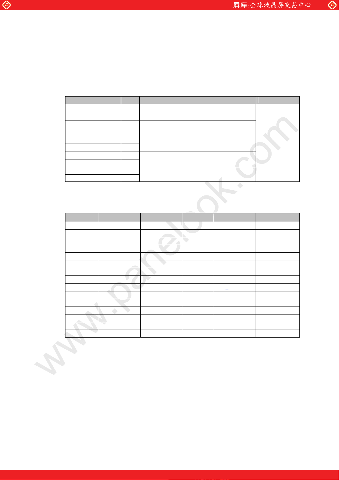
6 DISPLAY CHARACTERISTICS
6.1 General Specification
6.1.1 Opto-Electric Specifications
www.panelook.com
Module
ITEM C
rightness 1% white window 1,500 (Tpy) 1,400 (Tpy)
Peak B
l White Brightness Full white 190 (Tpy) 180 (Tpy)
Ful
X, Y co
DRCR1
Power C
Vi
Tvsync margin
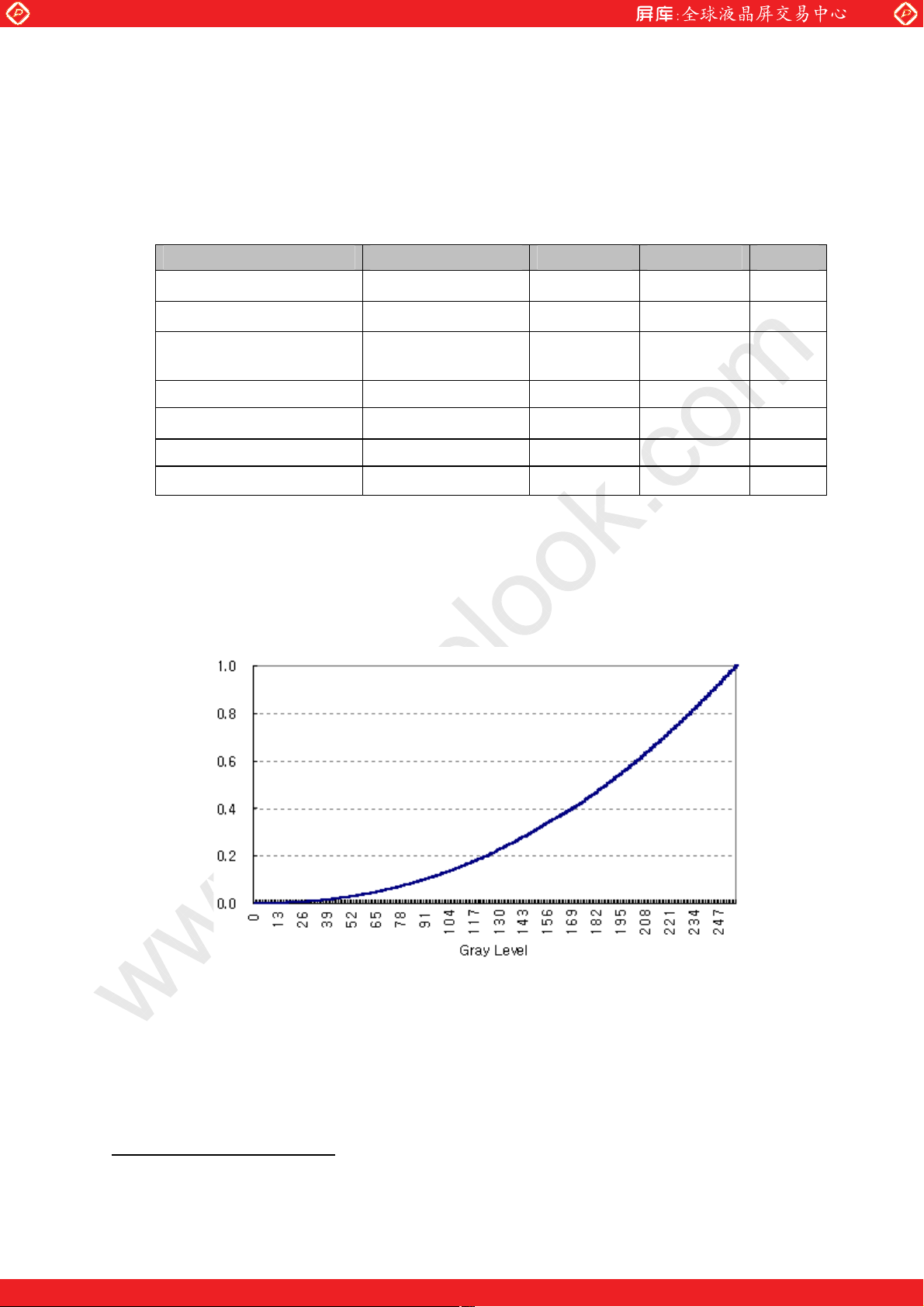
6.1.2 Gam
ordinate Full white
1% white window 10,000:1 (Tpy) 5,500:1 (Tpy) -
onsumption Full white 315 (Tpy) 315 (Tpy) Watt
2
ewing Angle
Full white 160 160 Degree
ma characteristics
ondition
60Hz 50Hz Un
0.285 / 0.290
± 0.015
ρ2 ρ2
PDP module is normally applied to the 2.2 gamma curve.
0.285 / 0.290
± 0.015
it
cd/
cd/
-
Hz
alized Gamma Curve
7/54 -
1
DRCR : Dark Room
2
It is the angle that m
Contrast Ratio.
eets 30% brightness level from center on full white pattern.
-
Figure 2 - Norm
CONFIDENTIAL
One step solution for LCD / PDP / OLED panel application: Datasheet, inventory and accessory!
www.panelook.com
Global LCD Panel Exchange Center
SAMSUNG SDI Corporation Specification Plasma Display
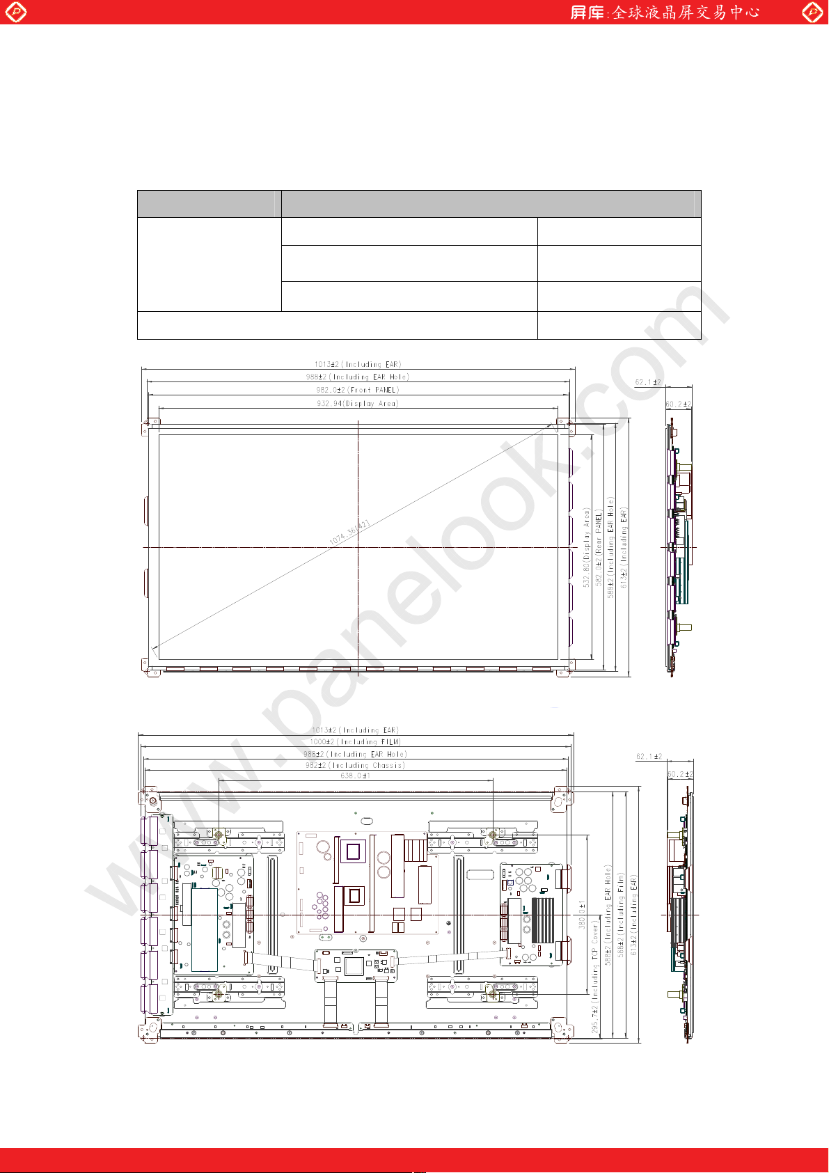
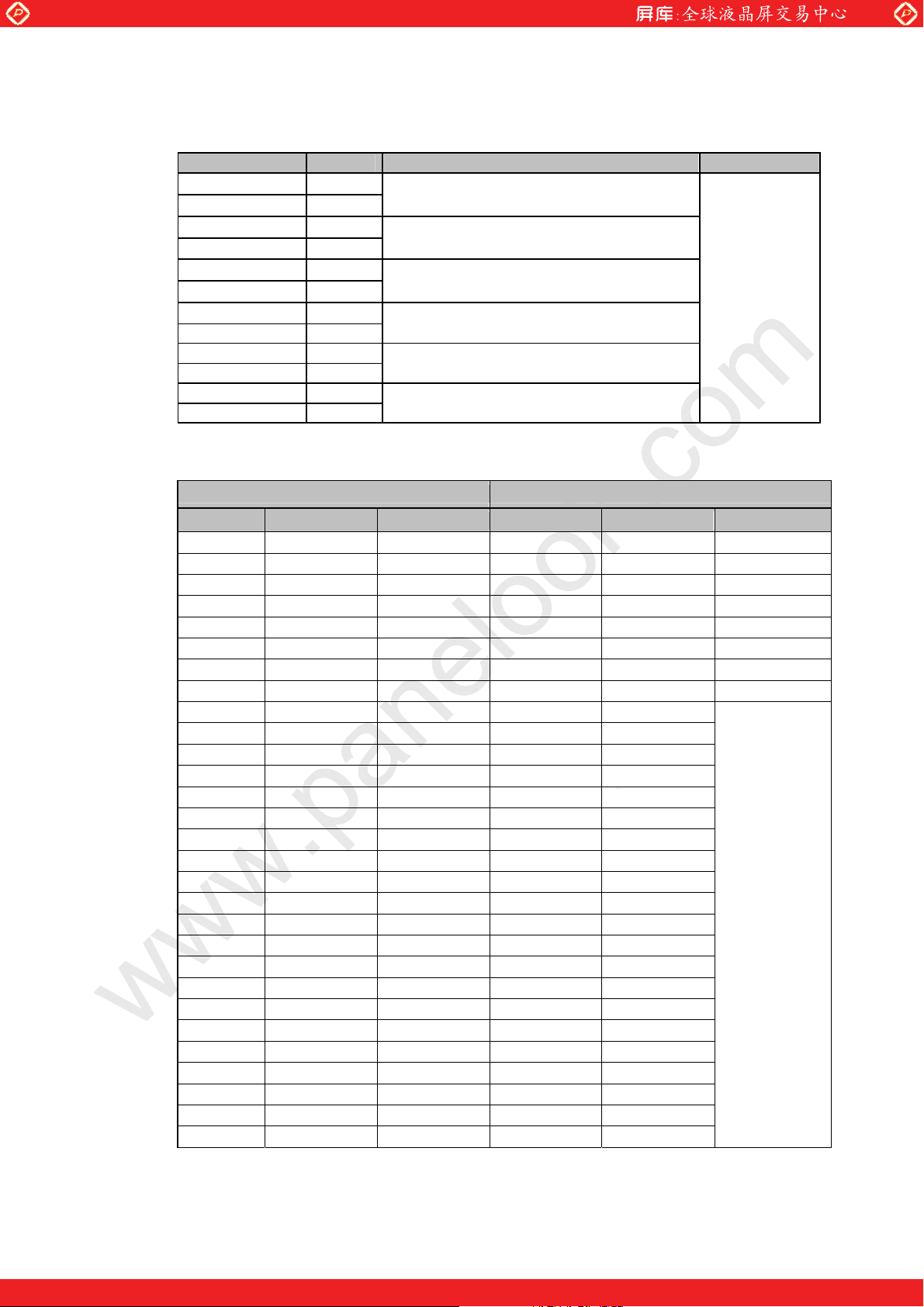
7 MECHANICAL PERFORMANCE
7.1 Mechanical Specifications
Item
Outer Dim
ension
www.panelook.com
Module
Rating
1013
613
62.1
± 2᎖
± 2
᎖
± 2
᎖
idth
W
Height
Thickness
eight Approximatly 17.2kg
W
Figure 3 - Mechanical Dim
Figure 4 - Mechanical Dim
ension of Front Side
ension of Rear Side
-
8/54 -
CONFIDENTIAL
One step solution for LCD / PDP / OLED panel application: Datasheet, inventory and accessory!
www.panelook.com
Global LCD Panel Exchange Center
SAMSUNG SDI Corporation Specification Plasma Display
7.2 Mechanical Test Method
www.panelook.com
Module
Item
Vibration
Stroke
Shock
Acceleration
The directions of
Frequency
Sweep
Durat
10 ~ 55 Hz
Rate 1 Octave/min
X,Y direction 0.35 mm (during 30min)
Z direction 0.175 mm (during 30min)
X,Y direction less than 20G
Z direction less than 10G
ion Time 11 ms
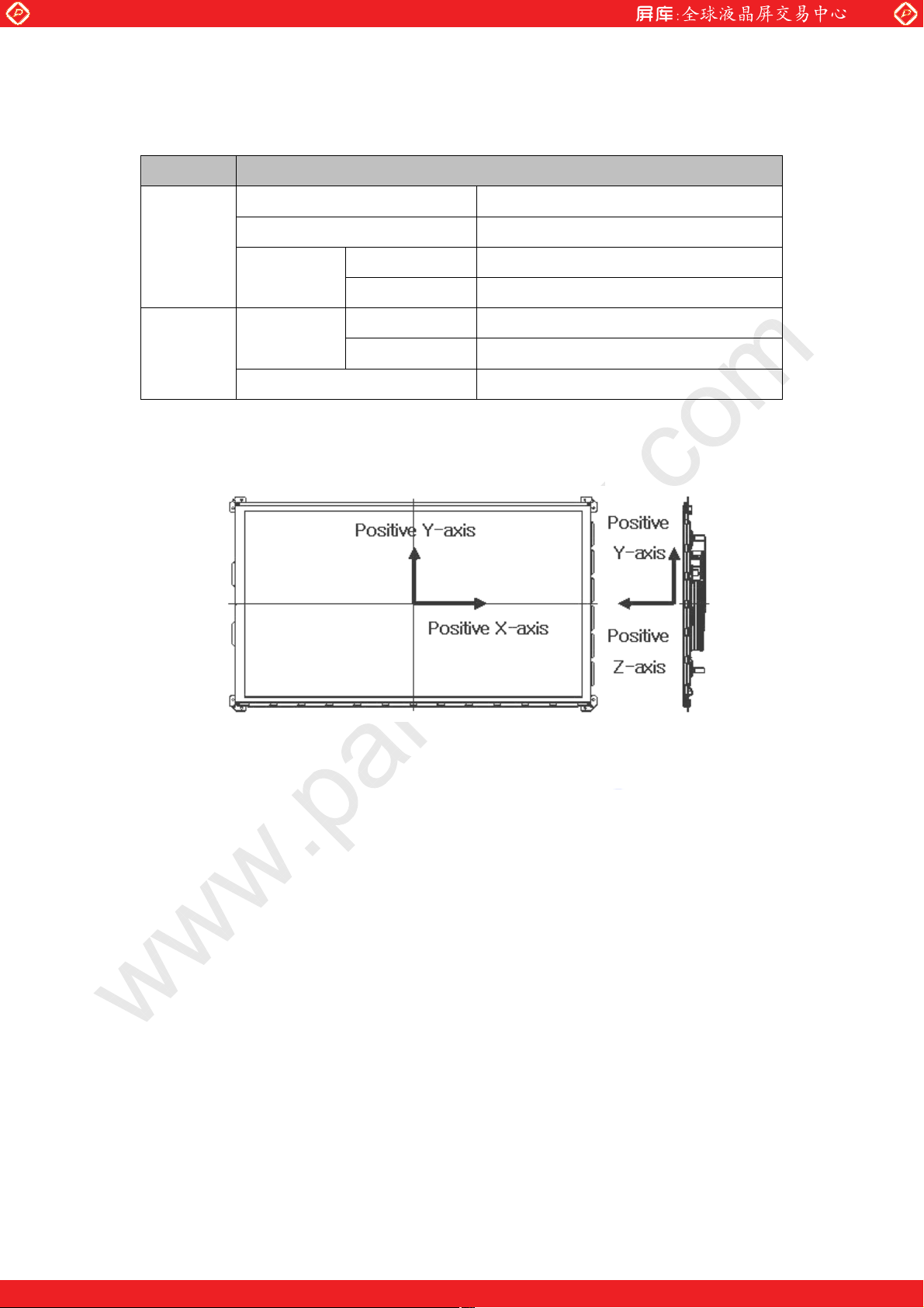
X-, Y- and Z-axis are as shown in Figure 7. The positive X direction
R
ating
is towards the right-side in the front view (to the left side in rear view); the positive Y
and Z are up ward and rear-to-front direction respectively.
Figure 5 – Test directions
-
9/54 -
CONFIDENTIAL
One step solution for LCD / PDP / OLED panel application: Datasheet, inventory and accessory!
www.panelook.com
Global LCD Panel Exchange Center
SAMSUNG SDI Corporation Specification Plasma Display
8 ENVIRONMENTAL PERFORMANCE
8.1 Operation
ITEM
perature 5 ~ ć 45ć 0 ~ ć 50ć
Tem
Hu
[NOTE]
1. Sound Noise is guaranteed till 1,600m
2. After operation at altitude higher than 1,600m, when using again within display
operational range (<1,600m) this product is still fully operational.
3. If tested after leaving PDP Module off-state under low temperature for a long time, for
example, more than 1 hr, it shall be operated for at least 15min.
midity
1
www.panelook.com
Module
R
atings
ecommended
R
20 ~ 70% RH 20 ~ 80% RH
bsolute maximum
A
.
8.2 Storage Environm
ITEM
Tem
perature
Humidity1 20 ~ 80% RH 5 ~ 85% RH
Air Pressure 850 ~ 1013 hPa 307 ~ 1013 hPa
ental Condition
R
-5ఁ ~ 45ఁ -20ఁ ~ 70ఁ
ecommended
atings
R
bsolute maximum
A
1
shall be no condensation.
It
-
10/54 -
CONFIDENTIAL
One step solution for LCD / PDP / OLED panel application: Datasheet, inventory and accessory!
www.panelook.com
Global LCD Panel Exchange Center
V
S CONN
C
O
(
)
V
S CONN
C
O
(
)
SAMSUNG SDI Corporation Specification Plasma Display
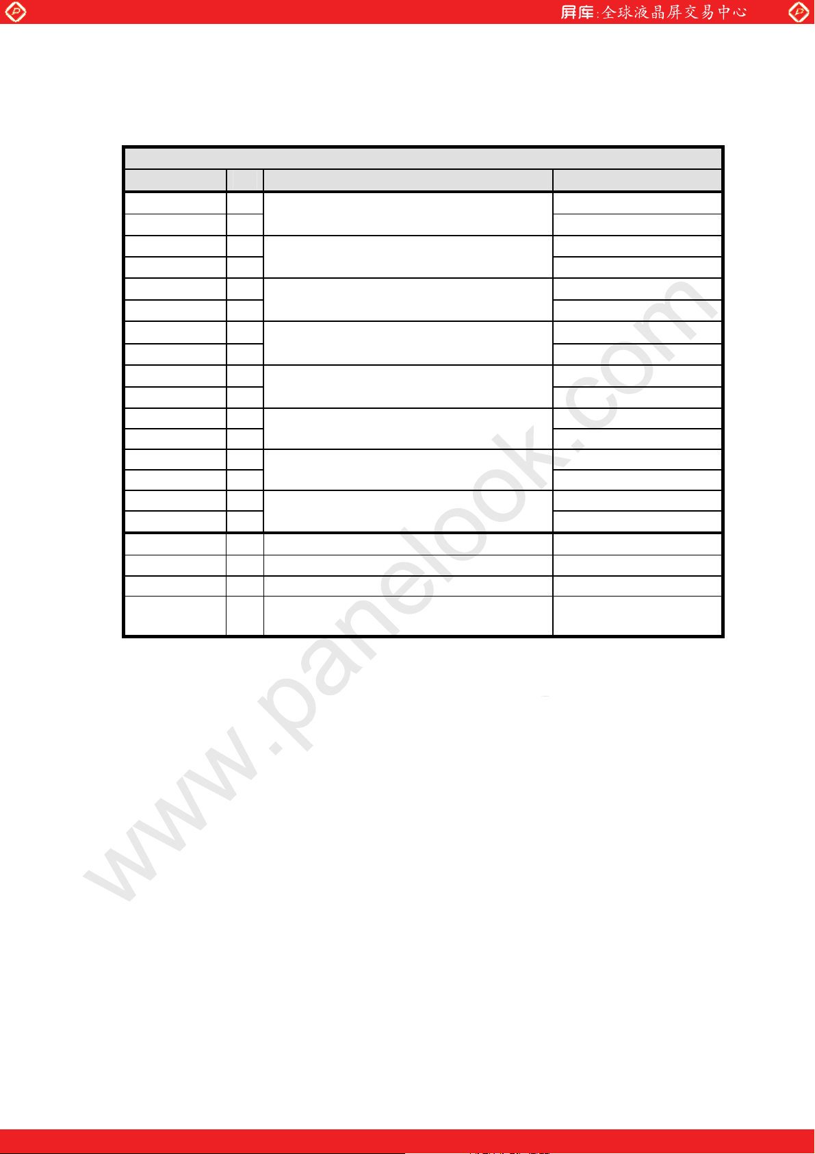
9 INTERFACE SIGNAL SPECIFICATION
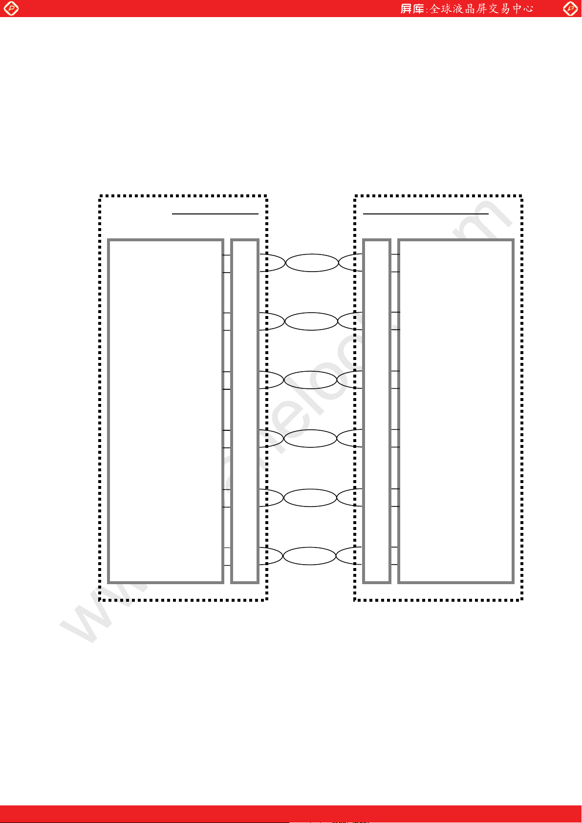
PDP Module uses an LVDS interface for the signal input. It is defined as like below.
For details, refer to the data sheets published by the LVDS IC m
9.1 LVDS Interface Block Diagram
www.panelook.com
Module
aker.
IMAGE BOARD
TxOUT0-
TxOUT0+
TxOUT1-
TxOUT1+
LVDS TRANSMITTER
L
D
TxOUT2-
TxOUT2+
E
TxCLKout-
TxCLKout+
T
R
Tx
TxOUT3-
TWIST
PAIR CABLE
LOGIC CONTROLLER
RxIN0-
RxIN0+
RxIN1-
RxIN1+
L
D
LVDS RECEIVER
RxIN2-
RxIN2+
E
T
R
Rx
RxCLKin-
RxCLKin+
RxIN3-
TxOUT3+
TxOUT4-
TxOUT4+
Figure 7 – Interface Block Diagram
RxIN3+
RxIN4-
RxIN4+
NOTE Do not connect or disconnect the cable of LVDS connector when PDP module
is turned on. Otherwise, LOGIC Controller could be damaged.
The length of the cable between image board and logic controller is recommended
One step solution for LCD / PDP / OLED panel application: Datasheet, inventory and accessory!
-
CONFIDENTIAL
not to be longer than 15cm and the cable shall be twisted.
11/54 -
www.panelook.com
Global LCD Panel Exchange Center
SAMSUNG SDI Corporation Specification Plasma Display
9.2 LVDS Connector and Pin Assignm
www.panelook.com
Module
ents
uUZWG
uUYG
uUXG
Figure 6 – UJU Electronics LVDS Connector, 1544A-3141R (Top View)
PIN No PIN NAM
1 GND
2 GND
3 RxIN04 RxIN0+
5 GND 15 RxCLKin- 25
6 GND
7
8
9
10
RxIN1- 17 N.C. 27 SCL
RxIN1+ 18 N.C. 28 GND
E
N.C. 19 RxIN3- 29 SDA
N.C. 20 RxIN3+ 30 GND
PIN No PIN NAM
11 RxIN2- 21
12 RxIN2+ 22 I2C_READY
13 GND 23 RxIN414 GND 24 RxIN4+
16 RxCLKin+ 26 GND
E
PIN No PIN NAM
VDS No_Picture
No_L
31 N.C.
E
GND
NOTE 1. Sustitute : ͷͺΈͶͷͻͲͶͻͲͲͿ
2. This connector is located on Logic Board.
-
12/54 -
CONFIDENTIAL
One step solution for LCD / PDP / OLED panel application: Datasheet, inventory and accessory!
www.panelook.com
Global LCD Panel Exchange Center
SAMSUNG SDI Corporation Specification Plasma Display
9.3 LVDS Signal
9.3.1 8BIT Application
Signal definition and Pin assignm
gnal
Si
RxIN0- I
RxIN0+ I
RxIN1- I
RxIN1+ I
RxIN2- I
RxIN2+ I
RxIN3- I
RxIN3+ I
RxCLKin
RxCLKin+ I
- I
www.panelook.com
Module
ents of LVDS Receiver are as follows:
I/O Funct
Disp
lay Data Signal:
R0, R1, R2, R3, R4, R5, G0
lay Data Signal:
Disp
G1, G2, G3, G4, G5, B0, B1
lay Data Signal:
Disp
B2, B3, B4, B5, Hsync, Vsync, DEN
Display Data Signal:
R6, R7, G6, G7, B6, B7
Dot Clock Signal:
CLK
ion
arks
Rem
LVDS signal
Table 1 –Input signal definition and pin assignm
PIN No PIN NAME SIGNAL PIN No PIN NAME SIGNAL
26 RxCLKOUT
27 R
29 R
30 R
32 R
33 R
34 RxOUT5 R(7) 54 RxOUT20 B(3)
35 R
37 R
38 R
39 RxOUT9 G(2) 3 RxOUT24 Hsync
41 R
42 R
43 RxOUT12 G(3) 7 RxOUT27 R(6)
45 R
xOUT0 R(0)
xOUT1 R(1) 49 RxOUT16 B(6)
xOUT2 R(2) 50 RxOUT17 B(7)
xOUT3 R(3) 51 RxOUT18 B(1)
xOUT4 R(4) 53 RxOUT19 B(2)
xOUT6 R(5) 55 RxOUT21 B(4)
xOUT7 G(0) 1 RxOUT22 B(5)
xOUT8 G(1) 2 RxOUT23 N.C.
xOUT10 G(6) 5 RxOUT25 Vsync
xOUT11 G(7) 6 RxOUT26 DEN
xOUT13 G(4)
Table 2 – Output signal pin assignm
Dot Clock
ents of LVDS Receiver (8Bit)
ents of LVDS Receiver (8Bit)
46 RxOUT14 G(5)
47 RxOUT15 B(0)
-
13/54 -
CONFIDENTIAL
One step solution for LCD / PDP / OLED panel application: Datasheet, inventory and accessory!
www.panelook.com
Global LCD Panel Exchange Center
SAMSUNG SDI Corporation Specification Plasma Display
9.3.2 10BIT / 12BIT / 13BIT Application
gnal
Si
RxIN0- I
RxIN0+ I
RxIN1- I
RxIN1+ I
RxIN2- I
RxIN2+ I
RxIN3- I
RxIN3+ I
RxCLKin
RxCLKin
RxIN4- I
RxIN4+ I
- I
+ I
www.panelook.com
Module
I/O Funct
Display Data Signal:
R2, R3, R4, R5, R6, R7,G2
lay Data Signal:
Disp
G3, G4, G5, G6, G7, B2, B3
Display Data Signal:
B4, B5, B6, B7, Hsync, Vsync, DEN
lay Data Signal:
Disp
R8, R9, G8, G9, B8, B9
Dot Clock Signal:
CLK
Disp
lay Data Signal:
R0, R1, G0, G1, B0, B1
ion
arks
Rem
LVDS signal
Table 3 –Input signal definition and pin assignm
LVDS 1 LVDS 2
PIN No PIN NAM
26 RxCLKOUT
27 R
29 R
30 R
32 R
33 R
34 RxOUT5 R(9) 34 RxOUT5 N.C.
35 R
37 R
38 R
39 RxOUT9 G(4) 39 RxOUT9
41 R
42 R
43 RxOUT12 G(5) 43 RxOUT12
45 R
46 R
47 R
49 RxOUT16 B(8) 49 RxOUT16
50 R
51 R
53 R
54 RxOUT20 B(5) 54 RxOUT20
55 R
1 R
2 R
3 R
5 R
6 RxOUT26
7 R
xOUT10 G(8) 41 RxOUT10
xOUT11 G(9) 42 RxOUT11
xOUT13 G(6) 45 RxOUT13
xOUT14 G(7) 46 RxOUT14
xOUT15 B(2) 47 RxOUT15
xOUT17 B(9) 50 RxOUT17
xOUT18 B(3) 51 RxOUT18
xOUT19 B(4) 53 RxOUT19
xOUT21 B(6) 55 RxOUT21
xOUT22 B(7) 1 RxOUT22
xOUT23 N.C. 2 RxOUT23
xOUT24 Hsync 3 RxOUT24
xOUT25 Vsync 5 RxOUT25
xOUT27 R(8) 7 RxOUT27
Table 4 – Output signal pin assignm
E
xOUT0 R(2)
xOUT1 R(3) 29 RxOUT1 R(1)
xOUT2 R(4) 30 RxOUT2 G(0)
xOUT3 R(5) 32 RxOUT3 G(1)
xOUT4 R(6) 33 RxOUT4 B(0)
xOUT6 R(7) 35 RxOUT6 B(1)
xOUT7 G(2) 37 RxOUT7
xOUT8 G(3) 38 RxOUT8
SIGNAL PIN No PIN NAM
Dot Clock
DEN 6 RxOUT26
ents of LVDS Receiver (10Bit)
ents of LVDS Receiver (10Bit)
E
26 RxCLKOUT Dot Clock
27 RxOUT0 R(0)
SIGNAL
N.C
-
14/54 -
CONFIDENTIAL
One step solution for LCD / PDP / OLED panel application: Datasheet, inventory and accessory!
www.panelook.com
Global LCD Panel Exchange Center
SAMSUNG SDI Corporation Specification Plasma Display
bol
Sym
RxARxA+
RxBRxB+
RxCRxC+
RxDRxD+
RxCLKRxCLK+
RxERxE+
RxFRxF+
RxCLKbRxCLKb+
SDA
SCL
RESET
I2C Ready
I/O Function Rem
I LVDS
I
I LVDS
I
I LVDS
I
I LVDS
I
I LVDS
I
I LVDS
I
I LVDS
I
I LVDS
I
I/O I2C serial data(Bi-direction) 3.3V CMOS
I Clock signal for SDA 3.3V CMOS
I No LVDS No Picture Flag 3.3V CMOS
O It indicates CLU ready for
Table 5 – Output signal pin assignm
www.panelook.com
Module
Interface Signal Function
Display Data Signal:
R4, R5, R6, R7, R8, R9, G4
Display Data Signal:
G5, G6, G7, G8, G9, B4, B5
Display Data Signal and Control Signal :
B6, B7, B8, B9, Hsync, Vsync, DEN
Display Data Signal :
R10, R11, G10, G11, B10, B11
Dot Clock Signal:
CLK
Display Data Signal:
R2, R3, G2, G3, B3, B3
Display Data Signal:
R0, R1, G0, G1, B0, B1
Dot Clock Signal:
CLKb
communication
ents of LVDS Receiver (12Bit)
arks
signal
LVDS signal
signal
LVDS signal
signal
LVDS signal
signal
LVDS signal
signal
LVDS signal
signal
LVDS signal
signal
LVDS signal
signal
LVDS signal
3.3V CMOS
-
15/54 -
CONFIDENTIAL
One step solution for LCD / PDP / OLED panel application: Datasheet, inventory and accessory!
www.panelook.com
Global LCD Panel Exchange Center
SAMSUNG SDI Corporation Specification Plasma Display
bol
Sym
RxARxA+
RxBRxB+
RxCRxC+
RxDRxD+
RxCLKRxCLK+
RxERxE+
RxFRxF+
RxCLKbRxCLKb+
SDA
SCL
RESET
I2C Ready
I/O Function Rem
I LVDS
I
I LVDS
I
I LVDS
I
I LVDS
I
I LVDS
I
I LVDS
I
I LVDS
I
I LVDS
I
I/O I2C serial data(Bi-direction) 3.3V CMOS
I Clock signal for SDA 3.3V CMOS
I No LVDS No Picture Flag 3.3V CMOS
O It indicates CLU ready for
Table 6– Output signal pin assignm
www.panelook.com
Module
Interface Signal Function
Display Data Signal:
R5,R6,R7,R8,R9,R10,G5
Display Data Signal:
G6,G7,G8,G9,G10,B5,B6
Display Data Signal and Control Signal:
B7,B8,B9,B10,Hsync,Vsync, DEN
Display Data Signal :
R11,R12,G11,G12,B11,B12,R0
Dot Clock Signal:
CLK
Display Data Signal:
R3,R4,G3,G4,B3,B4,G0
Display Data Signal:
R1,R2,G1,G2,B1,B2,B0
Dot Clock Signal:
CLKb
communication
ents of LVDS Receiver (13Bit)
arks
signal
LVDS signal
signal
LVDS signal
signal
LVDS signal
signal
LVDS signal
signal
LVDS signal
signal
LVDS signal
signal
LVDS signal
signal
LVDS signal
3.3V CMOS
-
16/54 -
CONFIDENTIAL
One step solution for LCD / PDP / OLED panel application: Datasheet, inventory and accessory!
www.panelook.com
Global LCD Panel Exchange Center
SAMSUNG SDI Corporation Specification Plasma Display
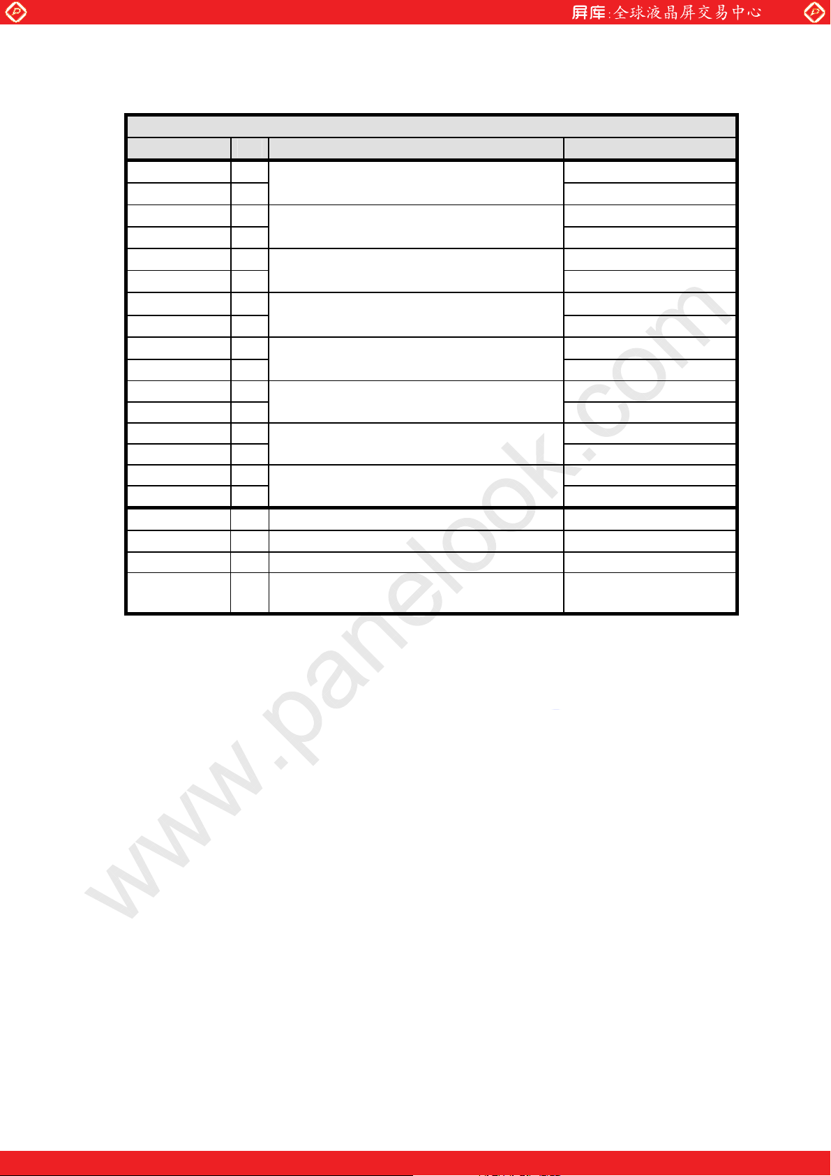
9.4 Electrical Characteristics
www.panelook.com
Module
9.4.1 Absolute Maxim
Parameter Condition Symbol Ratings Unit
LVDS
SC
MOS
3.3V C
um Ratings
Rx
IN0-/+, RxIN1-/+,
RxIN2-/+, RxIN3-/+,
RxIN4-/+, RxCLKin-/+
L, SDA, No_LVDS Flag Input Voltage Vi -0.3~3.6 V
I2C_READY Output Voltage Vo -0.3~3.6 V
9.4.2 Electrical Characteristics
Com
LVDS
eter
Param
Di
fferential input
High Threshold
Di
fferential input
Low Threshold
Input
current I
Voltage
Input
mbol
Sy
V
V
TH
V
V
TL
IN
VIH
V
IL
Common conditions : Ta = 25ఁ, Vcc = 3.3V
Input Voltage Vi -0.3~3.6 V
Input Current Ii -10~10 Ꮃ
mon conditions : Ta =25ఁ, Vcc = 3.3V
onditions
C
CM
CM
V
= +2.4V / 0V
IN
Vcc = 3.6V
=1.2V -
=1.2V -100
.
Min
- - ±10.0 Ꮃ
0.5×Vcc - 4.1 V
-0.5 - 0.3×Vcc V
Typ. Max
- 100 Ꭾ
- - Ꭾ
.
Unit
I2C
Input Capacitance VIN - - - 8 Ꮔ
Out
put Voltage
Out
put Current I
VOH I
-
V
OL
-
OL
= 8 Ꮄ 2.4
OH
- - 0.4 V
- - 10 Ꮄ
- - V
-
17/54 -
CONFIDENTIAL
One step solution for LCD / PDP / OLED panel application: Datasheet, inventory and accessory!
www.panelook.com
 Loading...