

Samsung S3C8847, S3C8849, S3P8849 Datasheet

S3C8847/C8849/P8849 PRODUCT OVERVIEW
1 PRODUCT OVERVIEW
SAM87 PRODUCT FAMILY
Samsung's SAM87 family of 8-bit single-chip CMOS microcontrollers offers a fast and efficient CPU, a wide
range of integrated peripherals, and various mask-programmable ROM sizes. Important CPU features include:
— Efficient register-oriented architecture
— Selectable CPU clock sources
— Release of Idle and Stop power-down modes by interrupt
— Built-in basic timer circuit with watchdog function
A sophisticated interrupt structure recognizes up to eight interrupt levels. Each level can have one or more
interrupt sources and vectors. Fast interrupt processing (within a minimum of six CPU clocks) can be assigned to
specific interrupt levels.
S3C8847/C8849/P8849 MICROCONTROLLERS
The S3C8847 microcontroller has a 24-Kbyte on-chip program memory and the S3C8849 has a 32-Kbyte. Both
chips have a 272-byte general-purpose internal register file. The interrupt structure has nine interrupt sources
with nine interrupt vectors. The CPU recognizes seven interrupt priority levels.
Using a modular design approach, the following peripherals were integrated with the SAM87 core to make the
S3C8847/C8849/P8849 microcontrollers suitable for use in color television and other types of screen display
applications:
— Four programmable I/O ports (26 pins total: 16 general-purpose I/O pins; 10 n-channel, open-drain
output pins)
— 4-bit resolution A/D converter (4 channels)
— 14-bit PWM output (Two channels: push-pull type, open-drain type)
— Basic timer (BT) with watchdog timer function
— One 8-bit timer/counter (T0) with interval timer and PWM mode
— One 8-bit general-purpose timer/counter (TA) with prescalers
— On-screen display (OSD) with a wide range of programmable features, including halftone control
signal output
The S3C8847 and the S3C8849 are available in versatile 42-pin SDIP package.
OTP
The S3C8847/C8849 microcontrollers are also available in OTP (One Time Programmable) version, named the
S3P8849. The S3P8849 microcontroller has an on-chip 32-Kbyte one-time-programmable EPROM instead of a
masked ROM. The KS88P8432 is comparable to the S3C8847/C8849, both in function and pin configuration.
1-1

PRODUCT OVERVIEW S3C8847/C8849/P8849
FEATURES
CPU
• SAM87 CPU core
Memory
• 24-Kbyte (S3C8847) or 32-Kbyte (S3C8849)
internal program memory
• 272-byte general-purpose register area
Instruction Set
• 78 instructions
• IDLE and STOP instructions added for powerdown modes
Instruction Execution Time
• 750 ns (minimum) with an 8 MHz CPU clock
Interrupts
• 9 interrupt sources with 9 vectors
• 7 interrupt levels
• Fast interrupt processing for select levels
General I/O
• Four I/O ports (26 pins total)
• Six open-drain pins for up to 6 V loads
• Four open-drain pins for up to 5 V loads
Pulse Width Modulation Module
• 14-bit PWM with two-channel output (push-pull
type, open-drain type)
• 8-bit PWM with four-channel, push-pull and opendrain
• PWM counter and data capture input pin
• Frequency: 5.859 kHz to 23.437 kHz with a 6
MHz CPU clock
On-Screen Display (OSD)
• Video RAM: 252 × 13-bits
• Character generator ROM: 384 × 18 × 16-bits
(384 display characters; fixed; 2, variable; 382)
• 252 display positions (12 rows × 21 columns)
• 16-dot × 18-dot character resolution
• 16 different character sizes
• Eight character colors
• Vertical direction fade-in/fade-out control
• Eight colors for character and frame background
• Halftone control signal output; selectable for
individual characters
• Synchronous polarity selector for H-sync and
V-sync input
8-Bit Basic Timer
• Three selectable internal clock frequencies
• Watchdog or oscillation stabilization function
Timer/Counters
• One 8-bit timer/counter (T0) with three internal
clocks or an external clock and interval timer
mode or PWM mode.
• One general-purpose 8-bit timer/counters with
interval timer mode (timer A)
A/D Converter
• Four analog input pins; 4-bit resolution
• 3.125 µs conversion time (8 MHz CPU clock)
1-2
Oscillator Frequency
• 5 MHz to 8 MHz external crystal oscillator
• Maximum 8 MHz CPU clock
Operating Temperature Range
• – 20°C to + 85°C
Operating Voltage Range
• 4.5 V to 5.5 V
Package Type
• 42-pin SDIP
S3C8847/C8849/P8849 PRODUCT OVERVIEW
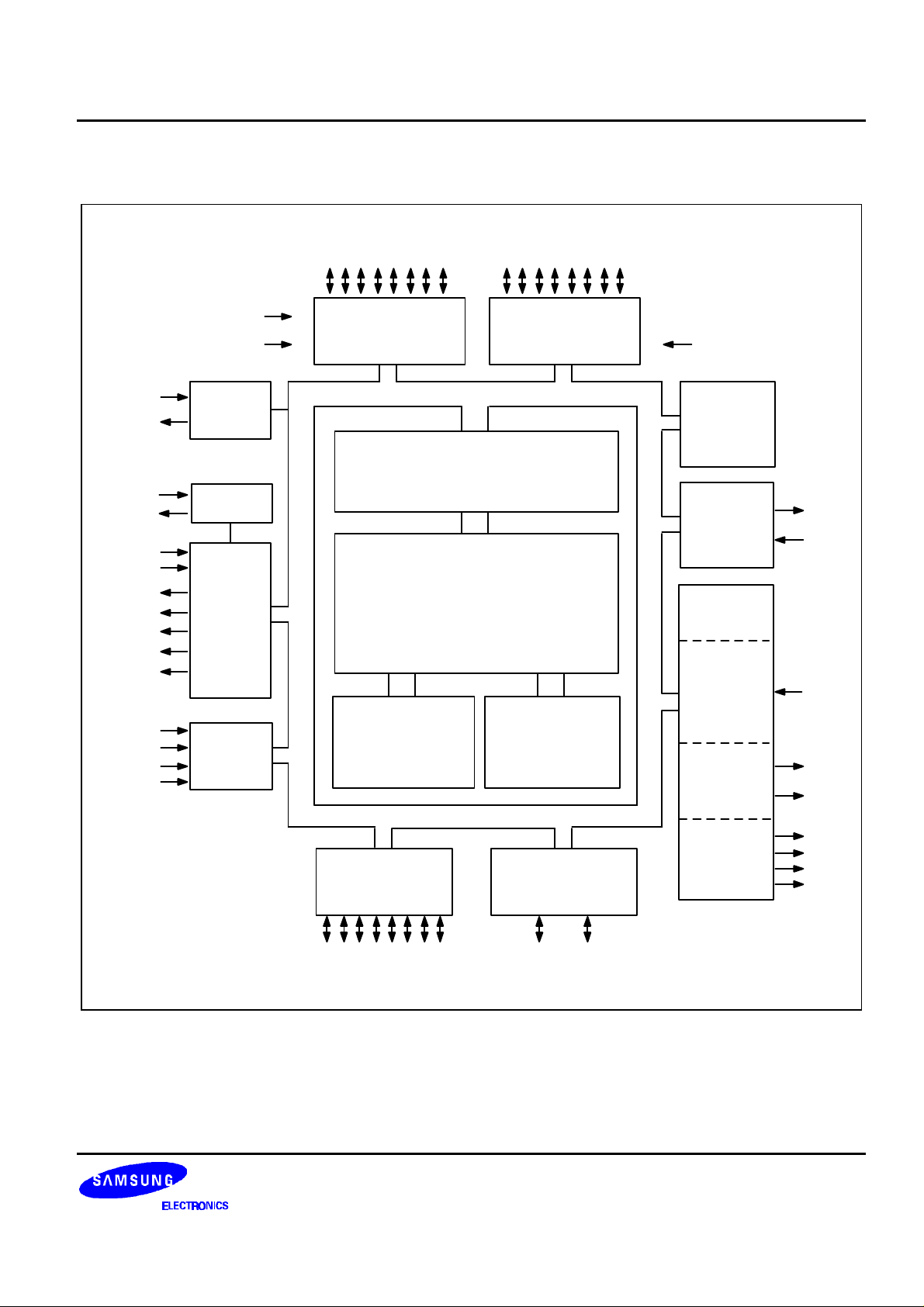
BLOCK DIAGRAM
X
OSC
OSC
H-sync
V-sync
Vgreen
Vblue
Vblank
OSDHT
ADC0
ADC1
ADC2
ADC3
X
IN
OUT
IN
OUT
Vred
RESET
INT0 - INT3
Main
Osc
L-C Osc
On-
Screen
Display
4-Bit
ADC
P0.0 - P0.7
Port 0 Port 1
SAM87 Bus
Port I/O and Interrupt
Control
SAM87 CPU
24/32-KByte
ROM
SAM87 Bus
Port 2
P1.0 - P1.7
272-Byte Register
File
Port 3
Test
Timer A
Timer 0
PWM
Block
PWM
Counter
and Data
Capture
14-Bit
PWM
8-Bit
PWM
TO
T0CK
CAPA
PWM0
PWM1
PWM2
PWM3
PWM4
PWM5
P2.0 - P2.7
Figure 1-1. Block Diagram
P3.0 - P3.1
1-3

PRODUCT OVERVIEW S3C8847/C8849/P8849
PIN ASSIGNMENTS
P2.5/PWM0
P2.1/PWM1
P2.2/PWM2
P2.3/PWM3
P2.4/PWM4
P2.0/PWM5
P2.6/T0
P1.7/T0CK
P3.0/ADC0
P3.1/ADC1
P0.6/ADC2
P0.7/ADC3
TEST
P1.0/INT0
P1.1/INT1
P1.2/INT2
P1.3/INT3
P1.4
P1.5
P1.6
P2.7/OSDHT
1
2
3
4
5
6
7
8
9
10
11
12
13
14
15
16
17
18
19
20
21
S3C8847/C8849
42-SDIP
(Top View)
42
41
40
39
38
37
36
35
34
33
32
31
30
29
28
27
26
25
24
23
22
Figure 1-2. S3C8847/C8849/P8849 Pin Assignment Diagram
P0.0
P0.1
P0.2
P0.3
P0.4
VSS2
CAPA
P0.5
VDD
RESET
XOUT
XIN
VSS1
OSCOUT
OSCIN
V-sync
H-sync
Vblank
Vred
Vgreen
Vblue
1-4
S3C8847/C8849/P8849 PRODUCT OVERVIEW
PIN DESCRIPTIONS
Table 1-1. S3C8847/C8849/P8849 Pin Descriptions
Pin Name Pin
Pin Description Circuit
Type
P0.0–P0.3 I/O General I/O port (4-bit), configurable for
digital input or n-channel open-drain, pushpull output.
Pins can withstand up to 5 V loads.
P0.4–P0.5 General I/O port (2-bit), configurable for
digital input or push-pull output.
P0.6–P0.7 General I/O port (2-bit), configurable for
digital input or n-channel open-drain output.
P0.6–P0.7 can withstand up to 5 V loads.
Multiplexed for alternative use as external
inputs, ADC2–ADC3.
P1.0–P1.3 I/O General I/O port (4-bit), configurable for
digital input or n-channel open-drain output.
P1.0–P1.3 can withstand up to 6 V loads.
Multiplexed for alternative use as external
interrupt inputs, INT0–INT3.
P1.4–P1.5 General I/O port (2-bit), configurable for
digital input or n-channel open-drain output.
P1.4–P1.5 can withstand up to 6 V loads.
High current port(10mA)
P1.6–P1.7 General I/O port (2-bit), configurable for
digital input or push-pull output.
Each pin has an alternative function.
P1.7: T0CK (Timer 0 clock input)
P2.0–P2.7 I/O General I/O port (8-bit). Input/output mode
or n-channel open-drain, push-pull output
mode are software configurable. Pins can
withstand up to 5 V loads.
Each pin has an alternative function.
P2.0: PWM5 (8-bit PWM output)
P2.1: PWM1 (14-bit PWM output)
P2.2: PWM2 (8-bit PWM output)
P2.3: PWM3 (8-bit PWM output)
P2.4: PWM4 (8-bit PWM output)
P2.5: PWM0 (14-bit PWM output)
P2.6: T0 (Timer 0 PWM and interval output)
P2.7: OSDHT (Halftone signal output)
P3.0–P3.1 I/O General I/O port (2-bit), configurable for
digital input or n-channel open-drain output.
P3.0–P3.1 can withstand up to 5 V loads.
Multiplexed for alternative use as external
inputs ADC0–ADC1.
Type
Numbers
2 39–42
3 38, 35
6 11–12
7 14–17
5 18–19
3 20, 8
2 1–7, 21
6 9–10
Pin
Share
Pins
(see pin
description)
ADC2–ADC3
INT0–INT3
T0CK
PWM0–
PWM5
T0, OSDHT
ADC0–ADC1
1-5
PRODUCT OVERVIEW S3C8847/C8849/P8849
Table 1-1. S3C8847/C8849/P8849 Pin Descriptions (Continued)
Pin Name Pin
PWM0–
Type
O Output pin for 14-bit PWM circuit 2 1, 2 P2.5, P2.1
Pin Description Circuit
Type
Pin
Numbers
Share
Pins
PWM1
PWM2–
PWM5
O Output pin for 8-bit PWM circuit 2 3–6 P2.2–P2.4,
P2.0
ADC0–ADC3 I Analog inputs for 4-bit A/D converter 6 9–12 P3.0–P3.1,
P0.6–P0.7
INT0–INT3 I External interrupt input pins 7 14–17 P1.0–P1.3
T0 O Timer 0 output (interval, PWM) 2 7 P2.6
T0CK I Timer 0 clock input 3 8 P1.7
OSDHT O Halftone control signal output for OSD 2 21 P2.7
Vblue, Vgreen
Vred, Vblank
H-sync,
O Digital blue, green, red, and video blank
4 22–25 –
signal outputs for OSD
I H-sync, V-sync input for OSD 1 26, 27 –
V-sync
OSCIN,
OSC
OUT
XIN, X
OUT
RESET
TEST –
I, O L-C oscillator pins for OSD clock frequency
– 28, 29 –
generation
I, O System clock pins – 31, 32 –
I System reset input pin 8 33 –
Test Pin (must be connected to VSS).
– 13 –
Factory test mode is activated when 12V is
applied.
VDD, V
V
SS2
SS1,
– Power supply pins – 34, 30, 37 –
CAPA I Input for capture A module 1 36 –
1-6
 Loading...