

Samsung S3C8475, S3C8478, S3P8475 Datasheet

S3C8478/C8475/P8475 PRODUCT OVERVIEW
1 PRODUCT OVERVIEW
SAM87RC PRODUCT FAMILY
Samsung's new SAM87RC family of 8-bit single-chip CMOS microcontrollers offers a fast and efficient CPU, a
wide range of integrated peripherals, and various mask-programmable ROM sizes.
Timer/counters with selectable operating modes are included to support real-time operations. Many SAM87RC
microcontrollers have an external interface that provides access to external memory and other peripheral
devices.
A sophisticated interrupt structure recognizes up to eight interrupt levels. Each level can have one or more
interrupt sources and vectors. Fast interrupt processing (within a minimum six CPU clocks) can be assigned to
one interrupt level at a time.
S3C8478/C8475 MICROCONTROLLER
The S3C8478/C8475 single-chip 8-bit microcontroller is designed for useful 10-bit resolution A/D converter,
UART, PWM application field. Its powerful SAM87RC CPU architecture includes. The internal register file is
logically expanded to increase the on-chip register space.
The S3C8478/C8475 has 8/16K bytes of on-chip program ROM. Following Samsung's modular design approach,
the following peripherals are integrated with the SAM87RC core:
— Large number of programmable I/O ports (42 SDIP: 34 pins, 44 QFP: 36 pins)
— One asynchronous UART module
— Analog-to-digital converter with eight input channels and 10-bit resolution
— One 8-bit basic timer for watchdog function
— One 8-bit timer/counter with three operating modes (Timer 0)
— One general-purpose 16-bit timer/counters with three operating modes (Timer 1)
The S3C8478/C8475 is a versatile general-purpose microcontroller that is ideal for use in a wide range of
electronics applications requiring complex timer/counter, PWM, capture, and UART.
It is available in a 42-pin SDIP or 44-pin QFP package.
OTP
The S3C8475 is an OTP (One Time Programmable) version of the S3C8478/C8475 microcontroller. The
S3C8475 microcontroller has an on-chip 16K-byte one-time-programmable EPROM instead of a masked ROM.
The S3C8475 is comparable to the S3C8478/C8475, both in function in D.C. electrical characteristics and in pin
configuration.
1-1

PRODUCT OVERVIEW S3C8478/C8475/P8475
FEATURES
CPU
• SAM87RC CPU core
Memory
• 272-byte general purpose register area
• 8/16K-byte internal program memory
Instruction Set
• 79 instructions
• IDLE and STOP instructions added for
power-down modes
Instruction Execution Time
• 333 ns at 12 MHz f
(minimum)
OSC
Interrupts
• 14 interrupt sources and 14 vectors
• Eight interrupt levels
• Fast interrupt processing
UART
• One UART module
• Full duplex serial I/O interface with three UART
modes
A/D Converter
• Eight analog input pins
• 10-bit conversion resolution
• 20 µs conversion time (10 MHz CPU clock)
Buzzer Frequency Output
• 200 Hz to 20 kHz signal can be generated
Oscillator Frequency
• 1 MHz to 12 MHz external crystal oscillator
• Maximum 12 MHz CPU clock
Operating Temperature Range
• – 40°C to + 85°C
General I/O
• Five I/O ports (total 36 pins)
• Four bit-programmable ports
• Two n-channel open-drain output port
Timer/Counters
• One 8-bit basic timer for watchdog function
• One 8-bit timer/counter with three operating
modes (timer 0)
• One 16-bit general-purpose timer/counters with
three operation modes (timer 1)
Operating Voltage Range
• 1.8 V to 5.5 V
Package Types
• 42-pin SDIP, 44-pin QFP
1-2
S3C8478/C8475/P8475 PRODUCT OVERVIEW
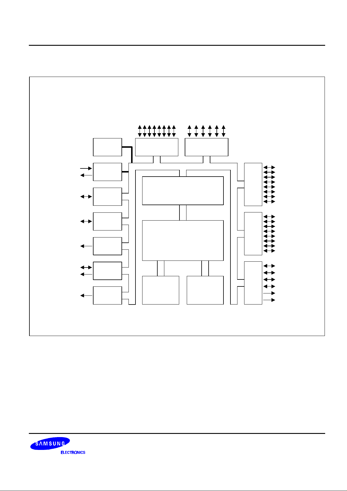
BLOCK DIAGRAM
P1.0-P1.5
T0, T1CK, T1,
P0.0-P0.7
BUZ, RxD, TxD
XIN
XOUT
T0(CAP)
T0(PWM)
T1(CAP)
T1(PWM)
ADC0-ADC7
P1.4/RxD
P1.5/TxD
P1.3/BUZ
Basic
Timer
OSC
Timer 0
Timer 1
ADC
UART
BUZ
Port 0
Port I/O and Interrupt
Control
SAM87RC CPU
8/16-Kbyte
ROM
272-byte
Register
Port 1
File
Port 2
Port 3
Port 4
P2.0-P2.7
INT0-INT7
P3.0-P3.7
ADC0-ADC7
P4.0-P4.3
P4.4-P4.5
Figure 1-1. Block Diagram
1-3
PRODUCT OVERVIEW S3C8478/C8475/P8475
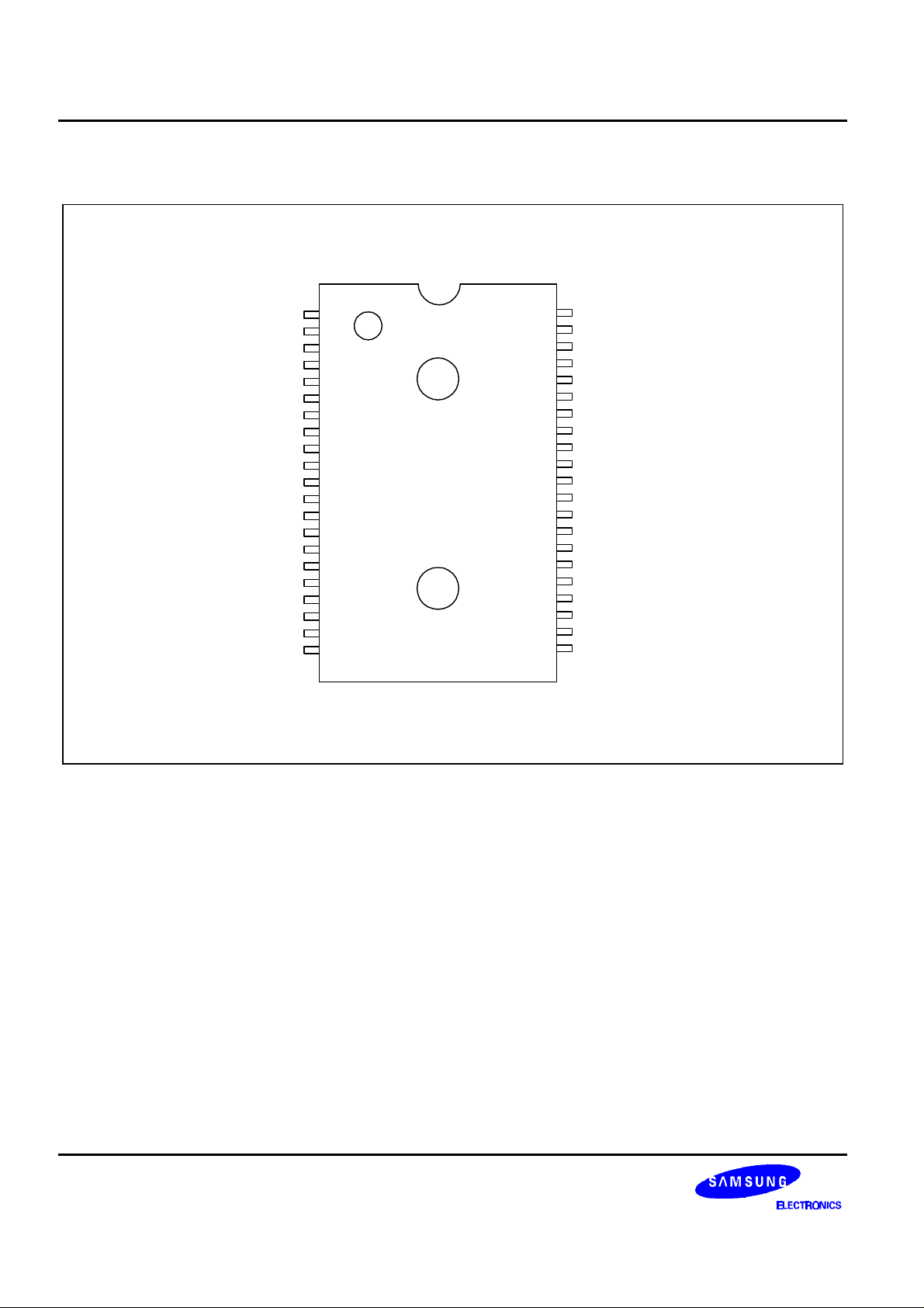
PIN ASSIGNMENTS
P0.7
P0.6
P0.5
P0.4
P0.3
P0.2
P0.1
P0.0
P4.3
P4.2
VDD
VSS
XOUT
XIN
TEST
P4.1
P4.0
RESET
P2.0/INT0
P2.1/INT1
P2.2/INT2
1
2
3
4
5
6
7
8
9
10
11
12
13
14
15
16
17
18
19
20
21
S3C8478
S3C8475
42-SDIP
(Top-View)
42
41
40
39
38
37
36
35
34
33
32
31
30
29
28
27
26
25
24
23
22
P1.0/T0 (CAP/PWM)
P1.1/T1CK
P1.2/T1 (CAP/PWM)
P1.3/BUZ
P1.4/RxD
P1.5/TxD
P3.7/ADC7
P3.6/ADC6
P3.5/ADC5
P3.4/ADC4
P3.3/ADC3
P3.2/ADC2
P3.1/ADC1
P3.0/ADC0
AVSS
AVREF
P2.7/INT7
P2.6/INT6
P2.5/INT5
P2.4/INT4
P2.3/INT3
1-4
Figure 1-2. Pin Assignment Diagram (42-Pin SDIP Package)
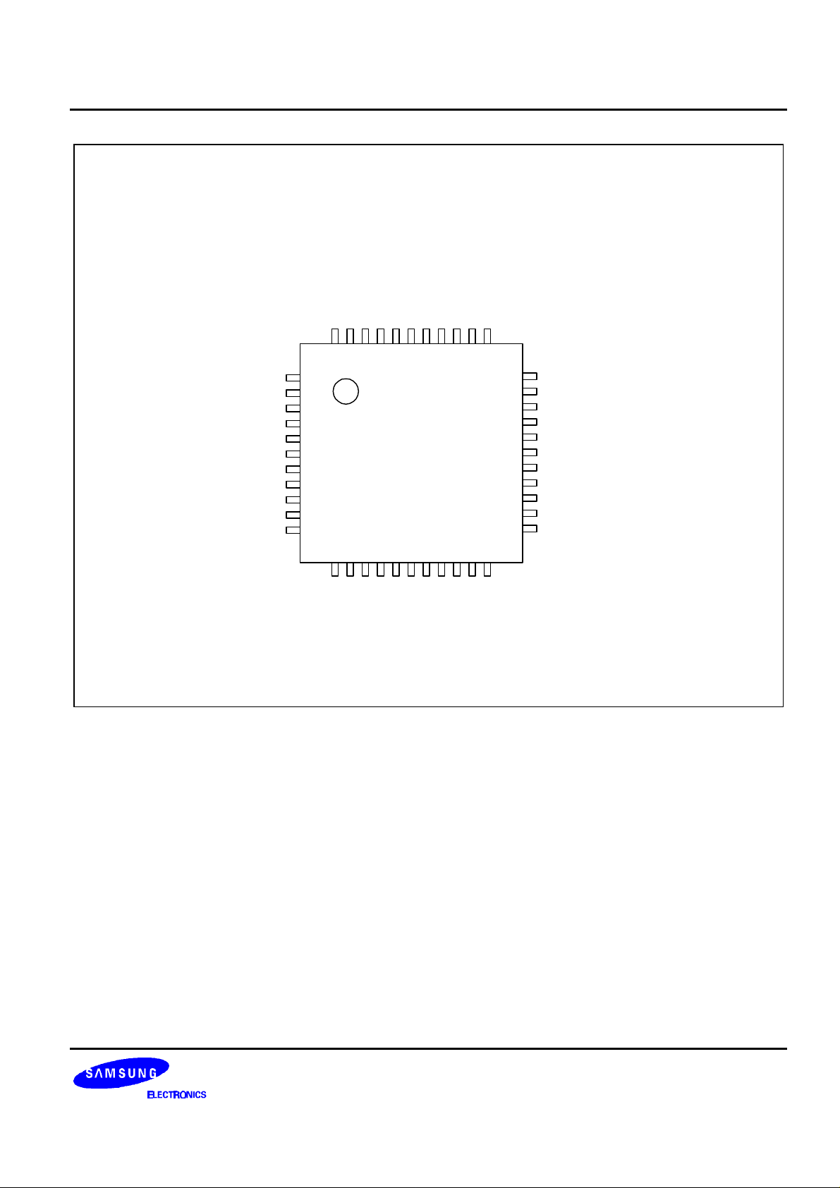
S3C8478/C8475/P8475 PRODUCT OVERVIEW
P4.4
P0.2
P0.3
P0.4
P0.5
P0.6
P0.7
P1.0/T0(CAP/PWM)
P1.1/T1CK
P1.2/T1(CAP/PWM)
P1.3/BUZ
4443424140393837363534
P0.1
P0.0
P4.3
P4.2
VDD
VSS
XOUT
XIN
TEST
P4.1
P4.0
1
2
3
4
5
6
7
8
9
10
11
S3C8478
S3C8475
44-QFP
(Top-View)
1213141516171819202122
33
32
31
30
29
28
27
26
25
24
23
P1.4/RxD
P1.5/TxD
P3.7/ADC7
P3.6/ADC6
P3.5/ADC5
P3.4/ADC4
P3.3/ADC3
P3.2/ADC2
P3.1/ADC1
P3.0/ADC0
AVSS
P4.5
RESET
P2.0/INT0
P2.1/INT1
P2.2/INT2
P2.3/INT3
P2.4/INT4
P2.5/INT5
P2.6/INT6
AVREF
P2.7/INT7
Figure 1-3. Pin Assignment Diagram (44-Pin QFP Package)
1-5
PRODUCT OVERVIEW S3C8478/C8475/P8475
Table 1-1. S3C8478/C8475 Pin Descriptions
Pin
Name
P0.0–P0.7 I/O Nibble-programmable I/O port for Schmitt trigger
P1.0–P1.5 I/O Bit-programmable I/O port for Schmitt trigger input
Pin
Type
Pin Description Circuit
input or push-pull, open-drain output. Pull-up
resistors are assignable by software.
or push-pull output. Pull-up resistors are assignable
by software. Port 1 pin can also by used as
Number
E 8-1
D 42-37
Pin
Number
(2-1,
43-38)
(37-32)
Share
Pins
T0, T1CK,
T1, BUZ,
RxD, TxD
alternative function (T0, T1CK, T1, BUZ, RxD, TxD)
P2.0–P2.7 I/O Bit-programmable I/O port for Schmitt trigger input
or push-pull output. Pull-up resistors are assignable
D 19-26
(13-20)
INT0-
INT7
by software. Port 2 pins can also be used as
external interrupt.
P3.0–P3.7 I/O Bit-programmable I/O port for Schmitt trigger input
or push-pull output. Pull-up resistors are assignable
F 29-36
(24-31)
ADC0-
ADC7
by software. Port 3 pins can also be used as A/D
converter by software.
P4.0–P4.3 I/O Bit-programmable I/O port for Schmitt trigger input
or push-pull, open-drain output. Pull-up resistors are
assingable by software.
E 17-16,
10-9
(11-10,
4-3)
P4.4–P4.5 O Push-pull output only C (44, 21) –
X
IN, XOUT
– Crystal or ceramic oscillator signal for system clock. – 14, 13
(8, 7)
RESET
TEST I Test signal input pin (for factory use only; muse be
I System reset signal input pin. B 18 (12) –
– 15 (9) –
connected to VSS)
–
–
–
AV
REF,
AV
SS
V
DD, VSS
– A/D converter reference voltage input and ground – 27, 28
(22, 23)
– Voltage input pin and ground – 11, 12
(5, 6)
T0 I/O Timer 0 capture input or PWM output pin D 42 (37) P1.0
T1CK I Timer 1 external clock input pin D 41 (36) P1.1
T1 I/O Timer 1 capture input or PWM output pin D 40 (35) P1.2
BUZ O 200Hz-20kHz frequency output for buzzer sound D 39 (34) P1.3
RxD I/O UART receive and transmit input or output D 38 (33) P1.4
TxD O UART transmit output D 37 (32) P1.5
INT0-INT7 I External interrupt input E 19-26
P2.0-P2.7
(13-20)
ADC0ADC7
NOTE: Pin numbers shown in parentheses "( )" are for the 44-pin QFP package.
1-6
I A/D converter input F 29-36
(24-31)
P3.0-P3.7
–
–
S3C8478/C8475/P8475 PRODUCT OVERVIEW
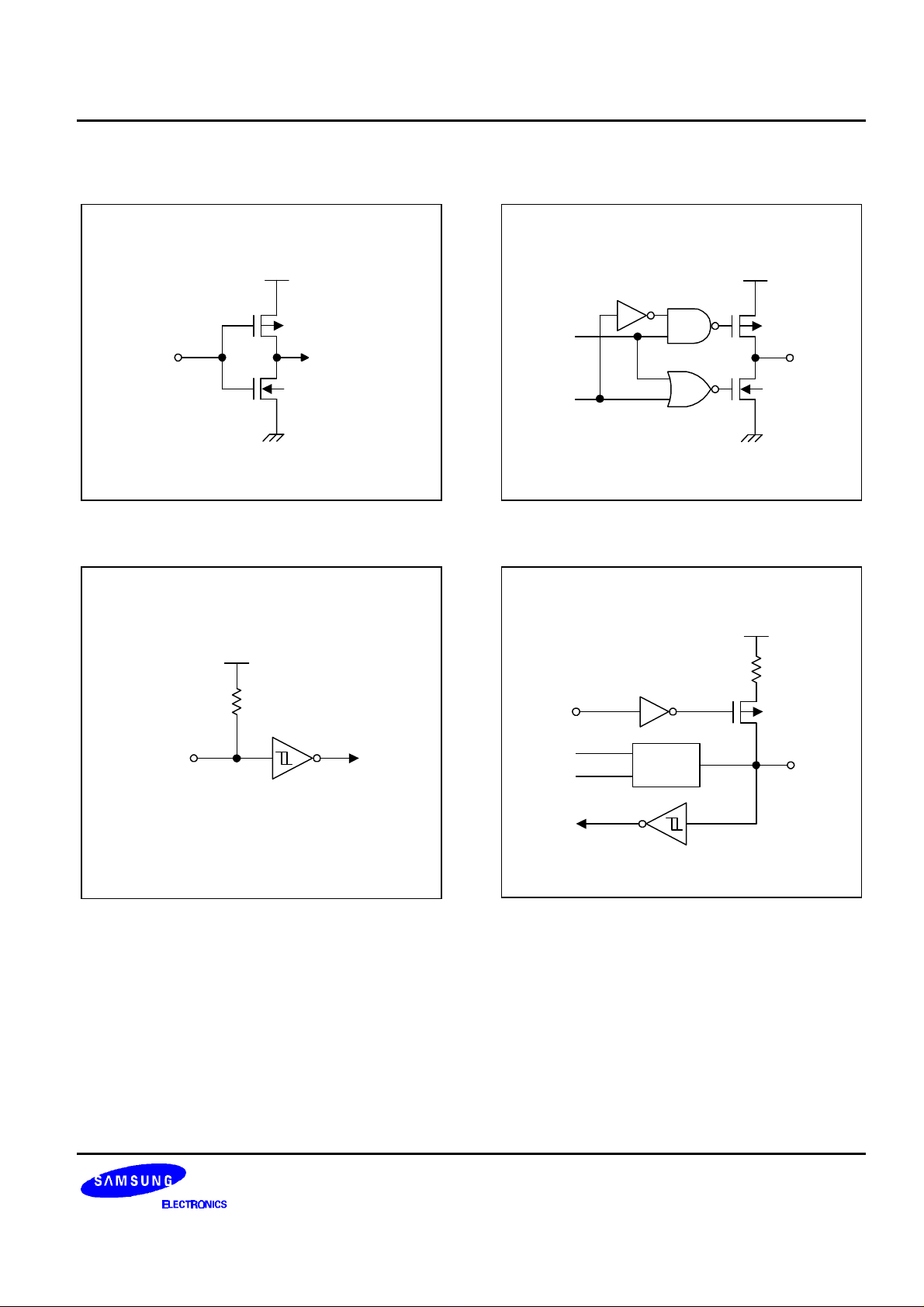
PIN CIRCUIT DIAGRAMS
VDD
P-Channel
In
N-Channel
Figure 1-4. Pin Circuit Type A
VDD
Pull-Up
Resistor
Data
Output
DIsable
Pull-up
Enable
VDD
P-Channel
Out
N-Channel
Figure 1-6. Pin Circuit Type C
VDD
In
Schmitt Trigger
Figure 1-5. Pin Circuit Type B
Data
Output
DIsable
Data
Circuit
Type C
Figure 1-7. Pin Circuit Type D
In/Out
1-7
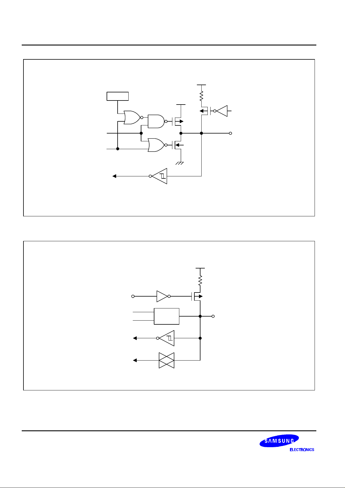
PRODUCT OVERVIEW S3C8478/C8475/P8475
VDD
Data
Output
DIsable
PNE
Schmitt Trigger
Figure 1-8. Pin Circuit Type E
VDD
47 K
Pull-up
Enable
P-CH
In/Out
N-CH
VDD
1-8
Pull-up
Enable
Data
Output
DIsable
Data
TO ADC
Circuit
Type C
Figure 1-9. Pin Circuit Type F
In/Out
 Loading...