

Page 1
S3P8245
ARM Blood Pressure Monitor
A
A
p
p
pllii
p
c
c
attii
a
o
o
n
n
N
N
ott
o
e
e
Revision 0.00
July 2010
© 2010 Samsung Electronics Co., Ltd. All rights reserved.
Page 2

Important Notice
The information in this publication has been carefully
checked and is believed to be entirely accurate at the
time of publication. Samsung assumes no
responsibility, however, for possible errors or
omissions, or for any consequences resulting from the
use of the information contained herein.
Samsung reserves the right to make changes in its
products or product specifications with the intent to
improve function or design at any time and without
notice and is not required to update this
documentation to reflect such changes.
This publication does not convey to a purchaser of
semiconductor devices described herein any license
under the patent rights of Samsung or others.
Samsung makes no warranty, representation, or
guarantee regarding the suitability of its products for
any particular purpose, nor does Samsung assume
any liability arising out of the application or use of any
product or circuit and specifically disclaims any and all
liability, including without limitation any consequential
or incidental damages.
"Typical" parameters can and do vary in different
applications. All operating parameters, including
"Typicals" must be validated for each customer
application by the customer's technical experts.
Samsung products are not designed, intended, or
authorized for use as components in systems intended
for surgical implant into the body, for other
applications intended to support or sustain life, or for
any other application in which the failure of the
Samsung product could create a situation where
personal injury or death may occur.
Should the Buyer purchase or use a Samsung product
for any such unintended or unauthorized application,
the Buyer shall indemnify and hold Samsung and its
officers, employees, subsidiaries, affiliates, and
distributors harmless against all claims, costs,
damages, expenses, and reasonable attorney fees
arising out of, either directly or indirectly, any claim of
personal injury or death that may be associated with
such unintended or unauthorized use, even if such
claim alleges that Samsung was negligent regarding
the design or manufacture of said product.
Copyright © 2010 Samsung Electronics Co., Ltd.
All rights reserved. No part of this publication may be reproduced, stored in a retrieval system, or transmitted in
any form or by any means, electric or mechanical, by photocopying, recording, or otherwise, without the prior
written consent of Samsung Electronics.
Samsung Electronics Co., Ltd.
San #24 Nongseo-Dong, Giheung-Gu
Yongin-City, Gyeonggi-Do, Korea 446-711
Contact Us: younghee46.won@samsung.com
TEL: (82)-(31)-209-3865
FAX: (82)-(31)-209-6494
Home Page: http://www.samsungsemi.com
Page 3

Revision History
Revision No. Date Description Author(s)
0.00 June 17, 2010 - Initial draft Xu Hui
Page 4

Table of Contents
1 OVERVIEW OF ARM BLOOD PRESSURE MONITOR...................................8
1.1 KEY Features of ARM Blood Pressure Monitor...........................................................................................9
1.2 System Block Diagram...............................................................................................................................10
1.3 Principles of Electronic Blood Pressure Monitor........................................................................................10
1.4 Process of Blood Measurement in Blood Pressure Monitor ......................................................................11
2 HARDWARE IMPLEMENTATION.................................................................13
2.1 Analog Signal Processing ..........................................................................................................................13
2.1.1 Introduction to MPS-3117 Pressure Sensor.......................................................................................14
2.1.2 Constant Current Driver Circuit ..........................................................................................................14
2.1.3 Differential amplifier circuit .................................................................................................................15
2.1.4 High Pass Filter Circult: 0.8Hz............................................................................................................16
2.1.5 Amplifier Circuit: 11x...........................................................................................................................17
2.1.6 Low-Pass Filter Circuit: 38Hz .............................................................................................................18
2.1.7 Pulse Rate Trigger Circuit ..................................................................................................................19
2.1.8 Interface between Analog Board and Main Board..............................................................................20
2.2 Microcontroller............................................................................................................................................21
2.2.1 Key Features of S3P8245 ..................................................................................................................22
2.2.2 Resource Assignment ........................................................................................................................23
2.2.3 LCD.....................................................................................................................................................24
2.2.4 Battery Voltage Detect........................................................................................................................24
2.2.5 I2C Device: EEPROM and Real Time Clock......................................................................................25
2.3 Pump Motor Driver Circuit..........................................................................................................................26
2.4 Valve Motor Driver circuit...........................................................................................................................27
2.5 Buzzer Enable and Driver Circuit...............................................................................................................28
2.6 Power Supply Circuit..................................................................................................................................29
3 SOFTWARE IMPLEMENTATION..................................................................30
3.1 Initialization ................................................................................................................................................31
3.2 Battery Voltage Detect ...............................................................................................................................31
3.3 Blood Pressure Monitor .............................................................................................................................33
3.3.1 Overview of Blood Pressure Monitor ..................................................................................................33
3.3.2 Monitor DC and AC Signals of Blood Pressure..................................................................................35
3.3.3 Analysis ..............................................................................................................................................36
3.4 EEPROM Write and Read Operations.......................................................................................................37
3.5 Interrupt Service Subroutine ......................................................................................................................38
3.5.1 Pulse Rate Input ISR ..........................................................................................................................38
3.5.2 User Button (Power On/Off) ISR ........................................................................................................39
3.5.3 User Button (Start, Up/Down, Delete, Save) ISR ...............................................................................40
Page 5

4 SCHEMATIC ..................................................................................................42
5 PCB LAYOUT ................................................................................................44
6 MEASUREMENT............................................................................................48
6.1 Test Environment.......................................................................................................................................48
6.2 Final Measurement Environment Setting...................................................................................................49
6.3 Test Result .................................................................................................................................................50
7 APPENDIX 1: BILL OF MATERIALS ............................................................51
8 APPENDIX 2: SOURCE CODE......................................................................54
Page 6

List of Figures
Figure Title Page
Number Number
Figure 1-1 Types of Blood Pressure Equipments ..................................................................................................9
Figure 1-2 System Block Diagram .......................................................................................................................10
Figure 1-3 DC and AC Components of Blood Pressure Signal and SBP/DBP Position......................................12
Figure 2-1 Analog Board (Driver, Diff-amp, 0.8Hz HPF, 11x Amp, 38Hz LPF, and Comparator) Circuit............13
Figure 2-2 MPS-3117 Pressure Sensor Appearance and Pin Assignment .........................................................14
Figure 2-3 Constant Current Driver and Pressure Sensor...................................................................................14
Figure 2-4 Diff-amplifier Circuit ............................................................................................................................15
Figure 2-5 High Pass Filter Circuit : 0.8Hz...........................................................................................................16
Figure 2-6 Amplifier Circuit : 11x..........................................................................................................................17
Figure 2-7 Low-Pass Filter Circuit : 38Hz ............................................................................................................18
Figure 2-8 Pulse Rate Trigger Circuit...................................................................................................................19
Figure 2-9 Interface between Analog Board and Main Board..............................................................................20
Figure 2-10 Microcontroller Circuit .......................................................................................................................21
Figure 2-11 LCD Function Diagram and External Driving Circuit ........................................................................24
Figure 2-12 Battery Voltage Detect Circuit...........................................................................................................24
Figure 2-13 EEPROM Circuit and Real-time Clock Circuit ..................................................................................25
Figure 2-14 Pump Motor Driver Circuit ................................................................................................................26
Figure 2-15 Valve Motor Driver Circuit.................................................................................................................27
Figure 2-16 Buzzer Enable and Driver Circuit......................................................................................................28
Figure 2-17 Power Supply Circuit ........................................................................................................................29
Figure 3-1 System Flow Chart .............................................................................................................................30
Figure 3-2 Battery Voltage Detect Flow Chart .....................................................................................................32
Figure 3-3 Blood Pressure Monitor Flow Chart....................................................................................................34
Figure 3-4 Monitor DC and AC of BP Flow Chart ................................................................................................35
Figure 3-5 Analysis Flow Chart ............................................................................................................................36
Figure 3-6 EEPROM Write and Read Operation Flow Chart...............................................................................37
Figure 3-7 Pulse Rate Input (External INT0) ISR Flow Chart ..............................................................................38
Figure 3-8 User Button (Power ON/OFF, External INT2) ISR Flow Chart...........................................................39
Figure 3-9 User Button (Start, Up/Down, Delete, Unit, Save, External INT4-7) ISR Flow Chart.........................41
Figure 4-1 Schematic of Analog Board ................................................................................................................42
Figure 4-2 Schematic of Main Board....................................................................................................................43
Figure 5-1 Main Board and Analog Board PCB Assembly (Top Layer)...............................................................44
Figure 5-2 Main Board and Analog Board PCB Assembly (Bottom Layer) .........................................................45
Figure 5-3 Main Board and Analog Board PCB (Top Layer) ...............................................................................45
Figure 5-4 Main Board PCB (Bottom Layer) ........................................................................................................46
Figure 5-5 Final Implementation of Blood Pressure Monitor (Main Board)..........................................................47
Figure 5-6 Final Implementation of Blood Pressure Monitor (Analog Board) ......................................................47
Figure 6-1 Final Measurement Environment Setting ...........................................................................................49
Figure 6-2 Blood Pressure Signals Measurement Waveform..............................................................................50
Page 7

List of Tables
Table Title Page
Number Number
Table 2-1 Microcontroller Resource Assignment .................................................................................................23
Table 7-1 Bill of Main Board Materials .................................................................................................................51
Table 7-2 Bill of Analog Board Materials..............................................................................................................53
Page 8

S3P8245_ARM BLOOD PRESSURE MONITOR_AN_REV 0.00 错误!未定义样式。 错误!未定义样式。
1 OVERVIEW OF ARM BLOOD PRESSURE
MONITOR
This application note describes an arm blood pressure monitor (BPM) based on Samsung's S3P8245
microcontroller. The reference design is intended for novices, who are not familiar with blood pressure monitor
system design. You can modify the design to build more complicated applications.
With rising living standards and increase in ageing among people, medical testing equipments have become
necessity for families. For instance, home blood pressure equipments have become increasingly popular with the
Chinese families.
Usually, these equipments are of two types:
• First is the Mercury sphygmomanometer. The main advantage of such equipment lies in its numerical stability.
However, the disadvantages include: patients cannot measure themselves if they are alone; the equipment
must be operated by healthcare professionals. This equipment can also result in significant visual observation
error. The measurement results can be different, depending on the doctor's experience and criterion, so it can
lead to subjectivity. The Mercury sphygmomanometer is bulky and not easy to carry (not portable).
• Second is the electronic Blood Pressure Monitor (BPM). The main advantage of such equipment include:
ease of use; patients without any professional training can also use this equipment. It is easy to record the
measured values with this equipment. Besides, it is lightweight and portable. Due to its advantages, more
families are using this equipment. From 2007 to 2010 alone, China's annual demand for electronic blood
pressure monitor grew to 350 million units.
Electronic blood pressure monitor are of two types:
• Wrist blood pressure monitor
• Arm blood pressure monitor
8
Page 9

S3P8245_ARM BLOOD PRESSURE MONITOR_AN_REV 0.00 错误!未定义样式。 错误!未定义样式。
Figure 1-1 shows all the above-mentioned blood pressure equipments.
a. Mercury Sphygmomanometer b. Wrist Blood Pressure Monitor c. Arm Blood Pressure Monitor
Figure 1-1 Types of Blood Pressure Equipments
1.1 KEY Features of ARM Blood Pressure Monitor
The key features of arm blood pressure monitor based on Samsung's S3P8245 microcontroller include:
• Measurement: Arm-type
• Measuring range: Pressure: 0 ~ 299mmHg (0 ~ 39.9kPa), Pulse: 40 ~ 180 beats/minute
• Accuracy: Pressure: ±4mmHg (±0.5kPa), Pulse: ±5%
• Pump method: Inflatable pump automatic inflate
• Deflate method: Release valve automatic deflate
• Measurement method: Oscillographic determination method
• Functions:
− User button: Power On/Off, Start, Up/Down, Delete, Save, and Unit
− Records up to 35 blood pressure monitoring records
− No user button operation; automatic shutdown after 30 seconds
• Power: 4x AA batteries or 6V DC power supply
• Battery life: 200 times measurement
• Operation temperature and humidity: +10℃ ~ +40℃; 30%RH ~ 85%RH
9
Page 10
S3P8245_ARM BLOOD PRESSURE MONITOR_AN_REV 0.00 错误!未定义样式。 错误!未定义样式。
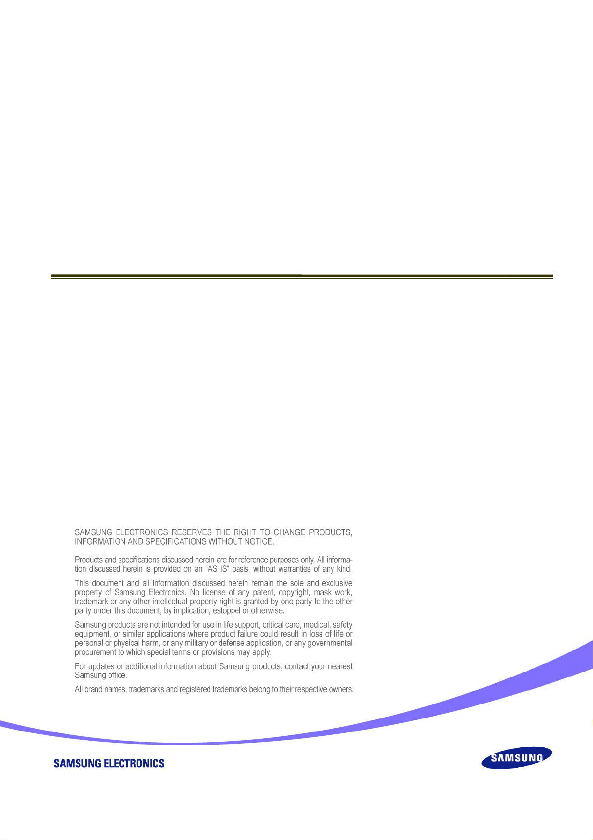
1.2 System Block Diagram
Note of BPM System Block
BT +6V : Battery +6 V
Power Mana. : Power Management
Cons. Cur. Driver : Constant Current Driver
Start But. : User Button
Power But. : User Button
RTC :
Real Timer Clock
: Not used
Cons. Cur .
Driver
2nd Order
HPF : 0 .8Hz
Amplifier
11 x
(Start)
(Power ON/OFF)
10 MHz
32. 768 KHz
Battery Vol . CPU
Pressure
Sensor
V+ V-
Diff - Amp
Analog Board V 1 . 0
2 nd Order
LPF : 38Hz
ADC2
ADC0
ADC1
BT
+6V
OSC
ADC
INT0
Pulse Rate
Trigger
Power Mana .
+5V
S3P8245
ROM
SIO
RAM
Ext. INT
INT1 INT2
Start
But .
EEPROM
3
I/OPWR
LCD
T1
TB
BUZ
INT4-INT7
Power
But .
Main Board V 2 .1
2
RTC
4
19 SEG * 4 COM
19
M
M
Other
User Button
LCD Screen
Pump
Motor
Valve
Motor
Figure 1-2 System Block Diagram
1.3 Principles of Electronic Blood Pressure Monitor
Typically, blood pressure can be described as systolic blood pressure (SBP) and diastolic blood pressure (DBP).
• Systolic blood pressure (SBP): The blood pressure is measured at the time of heart contraction, that is, when
blood hits the blood vessels.
• Diastolic blood pressure (DBP): The blood pressure is measured when the heart does not contract. If the cuff
pressure is equal to the blood pressure, blood begins to flow and produces a "cuff" sound. The blood pressure
is measured at this point (SBP). Once the cuff sound weakens, it gradually disappears. The blood pressure is
measured again at this point (DBP).
10
Page 11

S3P8245_ARM BLOOD PRESSURE MONITOR_AN_REV 0.00 错误!未定义样式。 错误!未定义样式。
1.4 Process of Blood Measurement in Blood Pressure Monitor
• The process of blood pressure measurement in the blood pressure monitor is described as follows:
• When the patient presses the Start button, the microcontroller opens the inflatable pump motor.
• The BPM system inflates up to 200mmHg. After reaching this value, it slowly deflates with the speed of
5mmHg per second.
• The pressure sensor outputs a signal through differential amplifier.
− One part of signal goes to the ADC0 channel to monitor the DC component of blood pressure signal.
− Other part goes to 0.8Hz second order high-pass filter to remove the DC component.
− Rest of the AC component of 11x amplification is inputted to the 38Hz second order low-pass filter (to filter
power and skin friction with the cuff of high-frequency noise and frequency interference, and to adjust the
signal in the range of 0 to 5V).
− One part of the filtered AC signal is sent to the pulse rate trigger circuit for generating trigger pulses that
starts the ADC module operation.
− Other part is sent to the ADC1 channel for calculating the amplitude of AC signal.
• Find the maximum peak-to-peak amplitude. Mark this point as MAP point.
• Before MAP point, determine the value that is the closest to 0.54*MAP. The corresponding DC component
value of this transient position specifies the systolic blood pressure (SBP) value.
• After MAP point, determine the point whose value is closest to 0.72*MAP. The corresponding DC component
value specifies the diastolic blood pressure (DBP) value.
• By using the internal timer to measure the interval between every two adjacent pulses, the system easily
obtains the pulse rate (PR) value.
• All the measurement results will be showed on the LCD screen.
11
Page 12
S3P8245_ARM BLOOD PRESSURE MONITOR_AN_REV 0.00 错误!未定义样式。 错误!未定义样式。
Figure 1-3 shows the system operation process, blood pressure, systolic and diastolic blood pressure signals, and
their position.
Pump Deflate
DC . BP
MAP
DBP
SBP
AC . BP
Figure 1-3 DC and AC Components of Blood Pressure Signal and SBP/DBP Position
12
Page 13
S3P8245_ARM BLOOD PRESSURE MONITOR_AN_REV 0.00 错误!未定义样式。 错误!未定义样式。
2 HARDWARE IMPLEMENTATION
2.1 Analog Signal Processing
The blood pressure monitor system needs a filter and an amplify circuit for the purpose of processing weak analog
signals and recognizing pulse signals. Such system is made of a single PCB board called the Analog Board. The
board provides a constant current driver (for pressure sensor), pre-amplifier (for pressure sensor's output weak
signal), high-pass filter, intermediate amplifier, low-pass filter, and pulse signal (which is sent to the MCU).
Figure 2-1
R2
4.7K ohm
P1.2/T1PWM
VHPF
shows a schematic diagram of the Analog Board.
VCC_+5V
R1
4.7K ohm
Q1
9012
J4
1
2
3
CON3
2
3
Amplifier: 11x
-
+
U4A
LM358
VCC_+5V
8 4
R28 10K ohm 1%R27 1K ohm 1%
R4
1.2K ohm
3
3
4
4
MPS-3117-006G_6_SOP
Pressure Sensor
VMAG
1
C13
104
2
U1
2
5
5
R31 49.9K ohm 1%
R5 0 ohm
AGND
R11 30K ohm 1%
1
1
6
6
R12 30K ohm 1%
R32 10K ohm 1%
GND
R6 1M ohm 1%
R20
2.4K ohm
AC Signal of BP
C8
104
R29 30K ohm 1%
2nd Order LPF: 38Hz
-
2
+
3
R13
1M ohm 1%
R16
1.3M ohm 1%
VCC_+5V
R21
182K ohm
P2.1/ADC1
C11
104
R7 1.3M ohm 1%
U2A
LM358
1
VCC_+5V
8 4
C4
104
C5
104
+
-
6
+
5
8 4
VDIF F
VDIF F
R23 100 ohm 1%
C6
10uF
R30 1K ohm 1%R25 1K ohm 1 %
7
LM358
U4B
VCC_+5V
R35 1M ohm 1%
R3 100 ohm 1%
C2
104
P2.0/ADC0
+
C3
104
R14 1K ohm 1%
R17 1M ohm 1% R18 1.5M ohm 1% R19 360K ohm 1%
C7
104
C9
VLPF
104
R33 5. 1M ohm 1%
DC Signal of Blood Pressure (BP)
C1
10uF
VCC_+5V
R8 1M ohm 1%
VCC_+5V
R34 10M ohm 1%
84
5
+
6
-
R22
100K ohm 1%
R24
50K ohm
VCC_+5V
R9 200K ohm 1%
U2B
LM358
R15 1K ohm 1%
2nd Order HPF: 0.8Hz
3
2
Pulse Rate Detector
7
641
-
LM311
7
+
U3
5
8
C12
104
R10 200K ohm 1%
VHPF
VCC_+5V
R26
10K ohm
P0.0/INT0
C10
Pulse Rate
104
Figure 2-1 Analog Board (Driver, Diff-amp, 0.8Hz HPF, 11x Amp, 38Hz LPF, and Comparator)
Circuit
13
Page 14
S3P8245_ARM BLOOD PRESSURE MONITOR_AN_REV 0.00 错误!未定义样式。 错误!未定义样式。
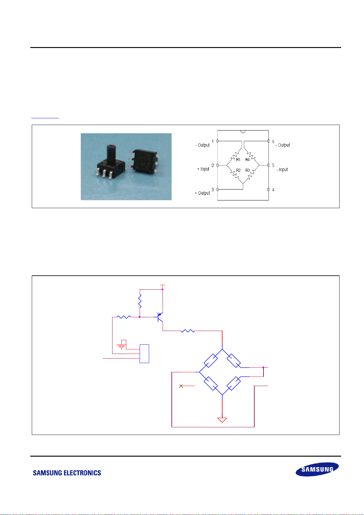
2.1.1 Introduction to MPS-3117 Pressure Sensor
MPS-3117 is a pressure sensor for blood pressure monitor from Taiwan Metrodyne Microsystem Corp. Its
dimension is 7mm×7mm×10mm, and its measurable pressure ranges from -299.95mmHg to +299.95mmHg.
MPS-3117 uses a constant source to drive the Wien Bridge. It sends the double-ended output differential signals
according to the pressure.
Figure 2-2
shows the appearance and pin assignment of MPS-3117 pressure sensor.
Figure 2-2 MPS-3117 Pressure Sensor Appearance and Pin Assignment
2.1.2 Constant Current Driver Circuit
The BPM system requires a constant current source to drive pressure sensor. The typical value of drive current is
1mA while the maximum value of drive current is 3mA.
VCC_+5V
R1
1
2
3
J4
CON3
4.7K ohm
Q1
9012
R4
1.2K ohm
3
3
4
4
MPS-3117-006G_6_SOP
U1
2
2
1
1
6
6
5
5
R2
4.7K ohm
P1.2/T1PWM
Figure 2-3 Constant Current Driver and Pressure Sensor
14
Page 15
S3P8245_ARM BLOOD PRESSURE MONITOR_AN_REV 0.00 错误!未定义样式。 错误!未定义样式。
+
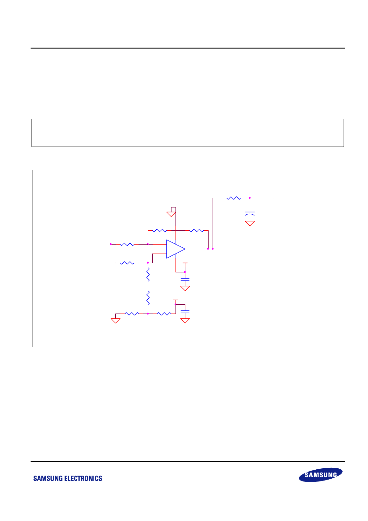
2.1.3 Differential amplifier circuit
In the BPM system, the differential amplifier plays the role of amplifying weak signal output from pressure sensor.
One way to do that is directly to the microcontroller as a DC signal of blood pressure. The other signal is provided
to the back analog circuits for filtering and amplification processing.
The diff-amplifier circuit output can be calculates as follows:
RR
+
67
VVV VVVV
( ) ( ) ( ) ( ) 76.667 ( )
=×−= ×−≈×−
DIFF IN IN IN IN IN IN
Rk
11
+− +− +−
11.3
MM
30
R7 1.3M ohm 1%
U2A
-
LM358
+
VCC_+5V
8 4
VCC_+5V
1
C4
104
C5
104
VDI FFVDI FF
R11 30K ohm 1%
R12 30K ohm 1%
R20
2.4K ohm
R6 1M ohm 1%
2
3
R13
1M ohm 1%
R16
1.3M ohm 1%
R21
182K ohm
Figure 2-4 Diff-amplifier Circuit
R3 100 ohm 1%
P2.0/ADC0
+
C1
10uF
15
Page 16

S3P8245_ARM BLOOD PRESSURE MONITOR_AN_REV 0.00 错误!未定义样式。 错误!未定义样式。
R
R
+
R
2.1.4 High Pass Filter Circult: 0.8Hz
The analog board of the BPM system uses 2nd order Butterworth high-pass filter circuit, whose transfer function is
calculated as follows:
2
()
HS
HPF
=
CC
2
SS
()
++
()()( )
8 9 10 2 3 8 9 10 17 18 19 2 3
+
23
R R CC R R R R R R CC
++ ++ + +
S
1
5
6
VCC_+5V
84
+
-
U2B
LM358
R15 1K ohm 1%R14 1K ohm 1%
7
VHPF
VDI FF
R8 1M ohm 1% R 9 200K ohm 1% R10 200K ohm 1%
C2
C3
104
104
R17 1M ohm 1% R18 1.5M ohm 1% R19 360K ohm 1%
Figure 2-5 High Pass Filter Circuit : 0.8Hz
Suppose the network coefficient a11 of 2nd order Butterworth is 1.414 and the angular frequency is 0.8x2π, while
the value of both C2 and C3 is 0.1uF. So, the values of R8+R9+R10 and R17+R18+R19 can be calculated as
follows:
CC
+
RR M
++ = = = Ω
8910
23
αω π
CC
2311
0.1 0.1 1.414 0.8 2
c
0.1 0.1
×× ××
1.41
RR M
++= = = Ω
17 18 19
( ) 1.41 0.1 0.1 (0.8 2 )
RRRCC M
++ Ω××× ×
891023
11
22
ωπ
c
2.86
16
Page 17

S3P8245_ARM BLOOD PRESSURE MONITOR_AN_REV 0.00 错误!未定义样式。 错误!未定义样式。
2.1.5 Amplifier Circuit: 11x
The signal coming from high-pass filter is weak and needs to amplify. Therefore, the system uses an 11x
magnification amplifier circuit.
R28 10K ohm 1%R27 1K ohm 1%
U4A
-
VHPF
2
3
+
8 4
LM358
1
VCC_+5V
C13
104
VMAG
Figure 2-6 Amplifier Circuit : 11x
17
Page 18

S3P8245_ARM BLOOD PRESSURE MONITOR_AN_REV 0.00 错误!未定义样式。 错误!未定义样式。
R
R
α
R
2.1.6 Low-Pass Filter Circuit: 38Hz
System uses 2nd order Butterworth low-pass filter circuit, whose transfer function is calculated as follows:
1
RRRCC
()
+
HS
()
LPF
=
2
SS
RRR
()
++
() ()
31 32 29 11 31 32 29 8 11
Suppose the network coefficient a11 of 2nd order Butterworth is 1.414 and the angular frequency is 38x2π, while
the value of both C2 and C3 is 0.1uF. So, the values of R31+R32 and R29 can be calculated as follows:
31 32 29 8 11
++
31 32 29
RRC R RRCC
++
1
Rk
+= = = Ω
31 32
== =Ω
29
( ) 59.3 0.1 0.1 (38 2 )
RRCC
11
+××××
31 32 8 11
11
CF
ωπμ
c
8
22
ωπ
c
1.414
38 2 0.1
××
59.3
29.3
k
C8
104
R31 49. 9K ohm 1%
VMAG
R32 10K ohm 1% R29 30K ohm 1%
C11
104
P2.1/ADC1
6
5
R23 100 ohm 1%
+
C6
10uF
R30 1K ohm 1%R25 1K ohm 1%
-
+
LM358
U4B
8 4
VCC _+5V
7
VLPF
Figure 2-7 Low-Pass Filter Circuit : 38Hz
18
Page 19

S3P8245_ARM BLOOD PRESSURE MONITOR_AN_REV 0.00 错误!未定义样式。 错误!未定义样式。
R
2.1.7 Pulse Rate Trigger Circuit
System uses a single, high-speed voltage differential comparator as the pulse rate trigger circuit. The signal,
which goes through the RC low-pass filter, will input to the positive side of comparator LM311. More reference
voltage is put on the negative side. When the signal is greater than the reference voltage, LM311 will be output
high. Otherwise, it holds the low level. Figure 2-8
shows the pulse rate trigger circuit.
R35 1M ohm 1%
VLPF
R33 5. 1M ohm 1%
VCC_+5V
C7
104
C9
104
R34 10M ohm 1%
R22
100K ohm 1%
R24
50K ohm
Figure 2-8 Pulse Rate Trigger Circuit
The reference voltage value is calculated as follows:
3
2
VCC _+5V
-
+
8
C12
104
VCC_+5V
641
LM311
7
U3
5
R26
10K ohm
P0.0/INT0
C10
104
RR
VV V
CMPREF DD
=× =×
24 24
++
22 24 24
5
RkR
100
By adjusting the potentiometer R24 value, you can select the appropriate reference voltage for pulse rate trigger
circuit. The actual value of R24 in this BPM system is 0.745V.
19
Page 20

S3P8245_ARM BLOOD PRESSURE MONITOR_AN_REV 0.00 错误!未定义样式。 错误!未定义样式。
2.1.8 Interface between Analog Board and Main Board
There are two interfaces (J8 and J9) between analog board and main board in the BPM system. One is called J9
that includes DC and AC signals of blood pressure and pulse rate trigger signal. Also, J9 provides +5V power,
both analog and digital ground. Both analog ground and digital ground is shorted by a 0Ω resistor. The other
interface is called J8 that controls the pressure sensor operation status. When P1.2 outputs low level, the sensor
turns on, else it turns off.
1
2
3
4
5
6
J9
CON6
P1.2/T1PWM
Pressure P1.2
ON 0
OFF 1
J8
1
2
3
CON3
R82 0 ohm
AGND
GND
VCC_+5V
P2.0/ADC0
P2.1/ADC1
AGND
P0.0/INT0
Figure 2-9 Interface between Analog Board and Main Board
20
Page 21

S3P8245_ARM BLOOD PRESSURE MONITOR_AN_REV 0.00 错误!未定义样式。 错误!未定义样式。
2.2 Microcontroller
In the reference design, Samsung’s S3P8245 is used as the microcontroller. The main function of this
microcontroller is to control both pump motor and valve motor, acquire and process both DC and AC of analog
signal, respond the pulse trigger and user button, and then display on the LCD screen.
The second function of this microcontroller is power management, record monitored results, and alarm patients
via buzzer.
P0.4/IN T4
P0.5/IN T5
P0.6/IN T6
P0.7/IN T7
C7 33pF
C11 33pF
C15 33pF
C16 33pF
J4
1
2
3
4
CON4
Y2
10MHz
Y3
32.768KHz
C10
100uFC8104
P0.1/I NT1
C17
104
VCC_+5V
+
1 2SW 5 SW KEY -SPST
VCC_+5V
R23
10K ohm
C18
0.1uF
VCC_+5V
R24
10K ohm
SEG9
SEG8
SEG7
SEG6P2.4/AD C4
SEG10
SEG11
SEG12
SEG13
SEG14
SEG15
P4.1/SEG17
P4.2/SEG18
P4.3/SEG19
P4.4/SEG20
P4.5/SEG21
P5.0/SEG24
P5.1/SEG25
P4.6/SEG22
SW6
KEY2
P5.2/SEG26
P5.3/SEG27
P5.4/SEG28
P5.5/SEG29
P5.6/SEG30
P5.7/SEG31
P3.0/TBPWM
P3.1
P3.2
P3.3
P3.4
VDD
GND
XOU T
XIN
TEST
XTI N
XTOU T
RESET
P0.0/I NT0
U4
1
SEG26/P5.2
2
SEG27/P5.3
3
SEG28/P5.4
4
SEG29/P5.5
5
SEG30/P5.6
6
SEG31/P5.7
7
P3.0/TBPWM
8
P3.1/TAOUT/ TAPWM
9
P3.2/TACLK
10
P3.3/TACAP/ SDAT
11
P3.4/SC LK
12
VDD
13
VSS
14
XOU T
15
XI N
16
TEST
17
XTI N
18
XTO U T
19
RESET
20
P0.0/I NT0
S3P8245_80_TQFP
80
P0.1/I NT1
P4.7/SEG23
79
SEG25/P5.1
P0.1/INT 121P0.2/INT 222P0.3/INT 323P0.4/INT 4
P0.2/I NT2
P0.3/I NT3
P4.0/SEG16
64
70
SEG1065SEG1166SEG1267SEG1368SEG1469SEG15
SEG16/P4.071SEG17/P4.172SEG18/P4.273SEG19/P4.374SEG20/P4.475SEG21/P4.576SEG22/P4.677SEG23/P4.778SEG24/P5.0
S3P8245
(80-TQFP-1212)
P0.5/INT 525P0.6/INT 626P0.7/INT 727P1.0/T1CAP28P1.1/T1CLK29P1.2/T1OUT/T1PWM30P1.331P1.4/BUZ32P1.5/SO33P1.6/SCK34P1.7/SI35P2.0/ADC036P2.1/ADC137P2.2/ADC238P2.3/ADC339P2.4/ADC4
24
P0.5/I NT5
P0.6/I NT6
P0.7/I NT7
P1.0
P1.1
P1.2/T 1PWM
P1.3
P1.4/BU Z
P1.5/SO
P1.6/SC K
P1.7/SI
P2.0/AD C0
P0.4/I NT4
P2.1/AD C1
SEG661SEG762SEG863SEG9
AVREF
P2.7/AD C7/VVLDR EF
P2.6/ADC6
P2.5/ADC5
40
P2.2/AD C2
P2.3/AD C3
Figure 2-10 Microcontroller Circuit
SEG5
SEG4
SEG3
SEG2
SEG1
SEG0
COM3
COM2
COM1
COM0
VLC2
VLC1
VLC0
AVSS
SEG4
SEG5
SEG6
SEG7
SEG0
SEG1
SEG[0...18]
SEG5
60
SEG4
59
SEG3
58
SEG2
SEG1
SEG0
COM3
COM2
COM1
COM0
VLC2
VLC1
VLC0
CA
CB
AVSS
AVREF
P2.7
P2.6
P2.5
VCC_+5V
R10
100K ohm
C12 0.1uF
R13
100K ohm
R14
100K ohm
R15 100K ohm
R17 0 ohm
R16 50 ohm
57
56
55
54
53
52
51
50
49
48
47
CA
46
CB
45
44
43
42
41
U2
BPMLCD_00598
C14
GND
+
103
11223344556677889
23
C13
10uF
VCC_+5V
SEG8
SEG2
COM3
SEG9
SEG3
COM2
COM1
SEG10
SEG11
9
12
1010111112
高压
低压
KPammHg
心
率
次/分
131314141515161617171818191920202121222223
P4.0/SEG16
SEG15
SEG14
SEG13
COM0
SEG12
P4.2/SEG18
P4.1/SEG17
21
Page 22

S3P8245_ARM BLOOD PRESSURE MONITOR_AN_REV 0.00 错误!未定义样式。 错误!未定义样式。
2.2.1 Key Features of S3P8245
The key features of S3P8245 include:
• Memory
− 16Kbytes One-time-program (OTP) ROM
− 544 bytes of data memory (RAM)
• 45 I/O (Sharing with LCD signal outputs)
• Interrupts
− 6 level, 8 vector, 8 internal interrupts
− 2 level, 8 vector, 8 external interrupts
• Timer
− Watch Timer for real-time and interval time measurement, clock generation for LCD and buzzer.
− 8-bit Timer/Counter A/B, Timer B can generate the carrier frequency
− 16-bit Timer/Counter 0/1
• 32 seg * 8 com LCD Controller/Driver
• 10-bit Analog to Digital Converter * 8 channels
• SIO * 1 channel
• Operating Temperature Range: -25℃ to 85℃
• Operating Voltage Range: 1.8V to 5.5V
• Package Type : 80-QFP-1420C, 80-TQFP-1212
22
Page 23

S3P8245_ARM BLOOD PRESSURE MONITOR_AN_REV 0.00 错误!未定义样式。 错误!未定义样式。
2.2.2 Resource Assignment
Table 2-1 Microcontroller Resource Assignment
No. Function Module Assignment Pin Note
DC & AC Signal of
1
Blood Pressure
Detector
ADC
One channel ADC for DC signal of
BP; Other channel for AC signal of
BP
P2.0/ADC0 (#36),
P2.1/ADC1 (#37)
2
channel
2
Pulse Rate
Detector
Interrupt
Rising edge trigger, calculate PR
@ ISR
3 LCD display LCD 4COM * 19 SEG
Timer Timer 0 generates 5ms interval - -
Rising edge trigger, ON/OFF @
ISR
Output high level to enable
GM6155-5.0
Updates the over-time counter
every 5ms. If the system is waiting
for over-time, no button is
4
Power
Management
Interrupt
I/O
Timer
pressed.
Falling edge trigger, execute
5 User Button Interrupt
function (Start, Up/Down,
Delete, Unit, Save) @ ISR
Timer
6 Pump Motor
I/O
Timer 1 is set in the PWM mode to
control the pump speed
Motor control 0-1, support
function:
Start/ Forward/ Reverse/ Stop
P0.0/INT0 (#20) -
COM0-3(#51-54),
SEG0-18(#55-73)
P0.2/INT2 (#22) -
P0.3 (#23) -
- -
P0.1/INT1 (#21),
P0.4/INT4 ~
P0.7/INT7 (#24-27)
Up to 5
channels
- -
P1.0-P1.1 (#28-29) -
-
7 Valve Motor Timer
8 EEPROM I/O
Timer B is set in repeating mode
to control the valve speed
One I/O for power control; Other
two I/O for I2C clock and data
P3.0/TBPWM (#7) -
P2.5-P2.7 (#41-43) -
9 RTC I/O Two I/O for I2C clock and data P3.3-P3.4 (#10-11) Not used
Generates the carrier frequency of
buzzer
Timer A is set in the PWM mode to
control the buzzer output time
One ADC channel for battery
voltage
P1.4/Buz (#32) -
- -
P2.2/ADC2 (#38) -
10 Buzzer
11
Battery Vol.
Detector
23
Buz
I/O Enables the buzzer output P1.3 (#31) -
Timer
ADC
Page 24

S3P8245_ARM BLOOD PRESSURE MONITOR_AN_REV 0.00 错误!未定义样式。 错误!未定义样式。
2.2.3 LCD
The internal LCD module in S3P8245 can directly drive up to 128-dot (32 segments × 4 commons) LCD panel.
The internal resistor bias can provide 1/2 bias, 1/3 bias, and 1/4 bias, without any bias pin or off chip resistor.
S3P8245 supports two kinds of LCD voltage driving circuit, that is, internal and external. This solution uses
external LCD voltage driving circuit.
The LCD panel used can display systolic blood pressure (SBP), diastolic blood pressure (DBP), pulse rate (PR),
diagnose result, and other system status (such as battery under-voltage). The drive method is +5V, 1/4 duty, and
1/3 bias.
Figure 2-11 LCD Function Diagram and External Driving Circuit
2.2.4 Battery Voltage Detect
Battery voltage is measured through R30 and R29 to ground. The relationship between voltage of P0.2/ADC2 port
and battery voltage is as follows:
R
VV V V
=× =× ≈×
ADC BAT BAT BAT
2
29
RR k k
++
29 30
k
10
10 5.1
0.662
When the battery voltage drops to 4.8V, the voltage of ADC2 input is about 3.179V. After battery voltage resumes
to 5.1V, the voltage of ADC2 increases to 3.377V.
C20 104
R29 10K ohm
P2.2/ADC2
R30 5.1K ohm VC C_+6V
Figure 2-12 Battery Voltage Detect Circuit
24
Page 25

S3P8245_ARM BLOOD PRESSURE MONITOR_AN_REV 0.00 错误!未定义样式。 错误!未定义样式。
2.2.5 I2C Device: EEPROM and Real Time Clock
The system uses a two-wire EEPROM 24C01 as blood pressure monitored data memory unit. Three I/O ports
(P2.5 ~ P2.7) are used to control this device. One is used to control the power supply when EEPROM is not used
during the main software process. Other two ports are the serial data and clock line between the MCU and
EEPROM interfaces.
Even though the final system does not use the RTC, this interface is used for hardware and software upgrades.
The system remains real-time clock circuit for high-resolution time and date application. The PCF8563 is a CMOS
real-time clock/calendar optimized for low power consumption. A programmable clock output, interrupt output, and
voltage-low detector are also provided. All addresses and data are transferred serially via a two-line bidirectional
I2C bus. Its maximum bus speed is 400 kbit/s. The built-in word address register is incremented automatically
after each written or read data byte.
1
2
3
VCC_+5V
U5
A0
VCC
A1
WP
A2
SCL
VSS4SDA
24C01_8_D IP
9012
8
7
6
5
R18 10K ohmQ2
R20 100 ohm
R21
R22
20K ohm
20K ohm
P2.5
P2.6
P2.7
Y1
32.768KH z
C9 CAP
C5
CAP VR
U3
1
OSCI
2
OSCO
3
INT
4
VSS
PCF 8563_8_DI P
VDD
CLKOUT
SCL
SDA
VCC_+5V
C6
104
8
7
6
5
R7
R11
20K ohm
20K ohm
P3.3
P3.4
Figure 2-13 EEPROM Circuit and Real-time Clock Circuit
25
Page 26

S3P8245_ARM BLOOD PRESSURE MONITOR_AN_REV 0.00 错误!未定义样式。 错误!未定义样式。
2.3 Pump Motor Driver Circuit
The BPM system has a 6V DC motor for cuff inflation. The scope of internal air pressure is restricted to measure
blood pressure (170 ~ 200mmHg). This driver circuit uses symmetry bridge type to support three motor modes,
including start, stop, forward, and reverse modes.
VCC_+6V
R35
Q5
9012
1K ohm
R39
Q8
9013
1K ohm
R32
1K ohm
R33
1K ohm
R34
1K ohm
Q6
9013
R31
1K ohm
R38
1K ohm
Q4
9012
MG1
1 2
MOTO R AC
Q7
9013
D1
1N4007
D2
1N4007
R36
1K ohm
Q9
9013
P1.0
P1.1
+
C23
10uF
C25
104
Figure 2-14 Pump Motor Driver Circuit
26
Page 27

S3P8245_ARM BLOOD PRESSURE MONITOR_AN_REV 0.00 错误!未定义样式。 错误!未定义样式。
2.4 Valve Motor Driver circuit
The BPM system uses a 6V DC motor for cuff deflation called valve motor. Use the timer B PWM output waveform
to control the speed of deflation.
P3.0/TBPWM
C26 104
R42
R45
1K ohm
10K ohm
VCC_+6V
12
Q10
9013
MG2
MOTO R
D3
1N4007
R43
0 ohm
Figure 2-15 Valve Motor Driver Circuit
27
Page 28

S3P8245_ARM BLOOD PRESSURE MONITOR_AN_REV 0.00 错误!未定义样式。 错误!未定义样式。
2.5 Buzzer Enable and Driver Circuit
When the User button is pressed (or system error occurs during measurement), the system will generate a buzzer
sound to grab the patient's attention. S3P8245 supports four kinds of frequencies for buzzer output. Therefore,
one I/O port connected through the buzzer module is used to control the buzzer frequency. The other I/O port is
used to enable or disable the buzzer output.
P1.4/BUZ
P1.3
1
2
R25
10K ohm
J3
CON2
R27
0 ohm
VCC_+5V
R19
1K ohm
Q3
9012
R26
1K ohm
R28
1K ohm
C19
+
47uF
LS1
Buzzer
Figure 2-16 Buzzer Enable and Driver Circuit
28
Page 29

S3P8245_ARM BLOOD PRESSURE MONITOR_AN_REV 0.00 错误!未定义样式。 错误!未定义样式。
2.6 Power Supply Circuit
GM6155-5.0 is an efficient linear voltage regulator with ultra low noise output, extremely low dropout voltage, and
extremely low ground current. The EN pin (#3) in this regulator controls the VOUT pin (#5), which supplies power
to the MCU.
When EN is low, VOUT has no output. On the contrary, when EN is high, VOUT outputs +5V power. After
pressing Key1 (Power ON/OFF user button), the +6V battery voltage is sent to ground through R37, SW7, D4,
and R46. The voltage of R46 is about 3.97V. When EN is high, VOUT will start to output +5V power to the
microcontroller. During the system initialization process, after the microcontroller starts operation, P0.3 outputs
high level. Then regardless of whether Key1 continues to be pressed or released, the EN pin will always be high
and the system will work properly. After that, if you press the Key1 again, the +6V battery voltage is sent to ground
through R37, SW7, and R40. The voltage of R40 will quickly rise to 3.97V and the diode D4 is off, leading to a
rising edge on the external interrupt input port P0.2/INT2.
After the MCU responds to this interrupt, P0.3 output low level, diode D6 is off and EN will be directly shorted to
ground through R46. As a result, VOUT will stop the output power supply to microcontroller. The system will enter
the power-down mode.
Figure 2-17
P0.2/ INT2
shows the power supply circuit of this blood pressure monitor system.
R41 100 ohm
C21
104
10K ohm
P0.3/ INT3
R40
D6
1N4007
R37
5.1K ohm
SW7
KEY1
D4
1N4007
R46
10K ohm
C22
+
470uF
VCC _+6V
C24
1
104
2
GM6155-5.0ST25R_5_SOT-25
VCC_+6V
U8
VIN
VOUT
GND
EN3BY P
1
2
1
2
J6
CON2
J7
CON2
5
4
VCC_+5V
Figure 2-17 Power Supply Circuit
C27
104
J5
1
2
CON2
VCC _+5V
C28
+
100uF
D5 LED
C29
104
R44
330 ohm
29
Page 30

S3P8245_ARM BLOOD PRESSURE MONITOR_AN_REV 0.00 错误!未定义样式。 错误!未定义样式。
3 SOFTWARE IMPLEMENTATION
Figure 3-1 shows the system flow chart with sequence of events in the software. After the microcontroller and
system initializes, if the Start button is pressed, the software enters the main loop. Battery voltage detect is used
for monitoring the battery voltage. The Blood Pressure Monitor starts a new blood pressure measurement for the
patient. After that, the software will respond to external user button operation, and execute the corresponding
function. When the system is waiting for User button out of time, the software will automatically shut down the
power supply.
Start
System Initialization
(MCU, Variable, LCD)
Start Button is
pressed?
Y
Battery Voltage Detect
Y
Y
Battery Vol. is
Under- voltage?
Blood Pressure Monitor
(SBP, DBP, PR)
System is
Over-time?
User Button Service
(Up/Down, Delete, Save)
Start Button
is pressed?
Switch off System Power
N
N
N
N
Y
End
Figure 3-1 System Flow Chart
30
Page 31

S3P8245_ARM BLOOD PRESSURE MONITOR_AN_REV 0.00 错误!未定义样式。 错误!未定义样式。
3.1 Initialization
Initialization involves three parts:
• First, initialize the microcontroller. All the function modules and control registers should be set to their proper
values.
• Second, initialize the system variables.
• Third, initialize the LCD, clear the display RAM area, and initialize all the LCD variables. Additionally, the
record data stored in the EEPROM should be read out before it is displayed on the LCD screen.
3.2 Battery Voltage Detect
After the Start button is pressed, the system will enter in the main routine.
• First, execute the battery voltage detector. The ADC channel #2 in S3P8245 is configured for battery voltage
detection.
• If the voltage value is lower than 4.9V, the software will set under-voltage flag (nSysFlag.6) and toggle the low
battery voltage label "
• Even if the voltage value is below 4.8V, the system will immediately turn off the power.
• On the other hand, if the battery voltage is up to 5.1V or more, the software will automatically clear the under-
voltage flag (nSysFlag.6) and turn off the corresponding label on the LCD screen.
" on the LCD screen.
31
Page 32

S3P8245_ARM BLOOD PRESSURE MONITOR_AN_REV 0.00 错误!未定义样式。 错误!未定义样式。
Start
Enanle ADC2 for
Battery Vol Sampling
N
Battery Vol.ls
= 4.9V?
Y
N
Battery Vol.ls
= 5.1V?
Y
Set Under-voltage flag
nSysFlag.6
Clear Under-voltage flag
nSysFlag.6
Turn OFF Low Bat. Vol.
label on LCD Screen
Toggle Low Bat Vol.
label on LCD Screen
N
Battery Vol.ls
= 4.8V?
Y
Switch off System power
End
Figure 3-2 Battery Voltage Detect Flow Chart
32
Page 33

S3P8245_ARM BLOOD PRESSURE MONITOR_AN_REV 0.00 错误!未定义样式。 错误!未定义样式。
3.3 Blood Pressure Monitor
This subroutine will complete a blood pressure measurement process for patient.
3.3.1 Overview of Blood Pressure Monitor
After initialization, the software inflates the pressure value to 200mmHg. The release valve remains closed during
this time. It then starts to exhaust the gas. Two seconds later, the external interrupt port 0 is enabled in order to
respond to the pulse signal.
In the ensuing process, the system monitors both DC signal and AC signals of blood pressure. As soon as the
software deflates the pressure value to 50mmHg, the system will end deflation. The pulse signal triggers the ADC
start operation. The software receives the effective DC and AC values of current cycle, that is, an effective pulse
signal. It can record up to 40 times of this effective pulse signal.
The software analyzes and diagnoses all monitored data. The final results are displayed on the LCD screen.
33
Page 34

S3P8245_ARM BLOOD PRESSURE MONITOR_AN_REV 0.00 错误!未定义样式。 错误!未定义样式。
Start Pump & OFF Valve
N
Stop Pump & Start Valve
input interrupt (INT0)
N
Start
Initialization
Pressure is
= 200mmHg
Y
Delay 2s
Enable Pulse Rate
Enable ADC0/1
(nSysFlag.0)?
Stop Valve
System is
Over-time?
N
Delay 400ms
Y
Y
Monitor DC & AC of BP
Pressure is
Y
= 50mmHg?
N
Monitor Time is
= 40?
Y
N
Analysis Monitor Results
Diagnose
Display SBP,DBP & PR
value on LCD
End
Figure 3-3 Blood Pressure Monitor Flow Chart
34
Page 35

S3P8245_ARM BLOOD PRESSURE MONITOR_AN_REV 0.00 错误!未定义样式。 错误!未定义样式。
3.3.2 Monitor DC and AC Signals of Blood Pressure
The subroutine monitors both DC and AC signals of blood pressure. Calculate the AC signal's peak-to-peak value
between two adjacent effective pulses. Determine the maximum and minimum values, and calculate the difference
between the two peaks. At the same time, the software will calculate the average DC signal value during the two
pulses.
Monitor ADC0(DC Of
BP) & ADC1(AC of BP)
Enable ADC0/1
N
(nSysFlag.0)?
Monitor DC & AC of BP
Amplitude-limit Filter for
Update Max. /Min./Sum.
DC value of BP
Update Max. / Min.
AC value of BP
Update DC/AC
Sampling Time
Start
Y
DC of BP
Sampling Time
is Over-time?
Y
Save to AC S tring Buffer
Save to DC String Buffer
Set ADC0/ADC1 enable
flag (nSysFlag.0)
Set Cur. Moni tor R esult
valid flag (nSysFlag.2)
End
N
Figure 3-4 Monitor DC and AC of BP Flow Chart
35
Page 36

S3P8245_ARM BLOOD PRESSURE MONITOR_AN_REV 0.00 错误!未定义样式。 错误!未定义样式。
3.3.3 Analysis
The subroutine analyzes the obtained DC and AC values of blood pressure to determine the SBP and DBP points.
• First, find the largest peak-to-peak value in AC data buffer. Mark this point as MAP point.
• Second, search the point whose value is the closest to 0.54*MAP. This point is located in front of the MAP
point. The corresponding average value in DC data buffer specifies the systolic blood pressure (SBP) value.
• Search the point whose value is the closest to 0.72*MAP. This point is located behind the MAP point. The
corresponding average value of DC data specifies the diastolic blood pressure (DBP) value.
• Finally, the PR value for patient can be determined by analyzing the entire pulse rate (PR) data.
Start
Find Max. AC of BP
Calculate
0.54*Max. AC of BP
Find preceding point which is
close to 0 .54*Max . AC
Calculate Practical SBP
Calculate
0.72*Max. AC of BP
Find subsequent point which
is close to 0.72*Max. AC
Calculate Practical DBP
Calculate Practical PR
End
Figure 3-5 Analysis Flow Chart
36
Page 37

S3P8245_ARM BLOOD PRESSURE MONITOR_AN_REV 0.00 错误!未定义样式。 错误!未定义样式。
3.4 EEPROM Write and Read Operations
The system uses two wires EEPROM 24C01(1K, 128*8) as storage unit, which can record up to 35 blood
pressure monitor results, including SBP, DBP, and PR values. 24C01 is an EEPROM chip with I2C interface.
Read and write operations on the bytes have a special definition, as follows:
Write Start
Varibles Initialization
Send START Signal
Send C ontrol Byte
(1010xxx0B)
Receive ACK
N
Signal?
Y
Send Word Address
(0xxxxxxxB)
Receive ACK
N
Signal?
Y
Send Data to EEPROM
(xxxxxxxxB)
Read Start
Varibles Initialization
Send START Signal
Send Control Byte
(1010xxx0B)
Receive ACK
N
Signal?
Y
Send Word Address
(0xxxxxxxB)
Receive ACK
N
Signal?
Y
Re-send START Signal
Receive ACK
N
Signal?
Send STOP Signal
Delay 5ms
Write End
Figure 3-6 EEPROM Write and Read Operation Flow Chart
37
Send Control Byte
(1010xxx1B)
Y
Receive ACK
N
Signal?
Send STOP Signal
Delay 5ms
Y
Read Data from
EEPROM
Read End
Page 38

S3P8245_ARM BLOOD PRESSURE MONITOR_AN_REV 0.00 错误!未定义样式。 错误!未定义样式。
3.5 Interrupt Service Subroutine
The BPM software has several important interrupt service subroutines (ISR), including pulse rate input ISR and
user button ISR.
3.5.1 Pulse Rate Input ISR
The subroutine can calculate the pulse rate and set (or clear) ADC0/ADC1 enable flag corresponding to different
conditions. Figure 3-7
shows the flow chart of this interrupt service routine.
N
N
ISR Enter
Clear Ext. INT0
pending bit
Delay 2ms
(for S/W debounce)
P0.0/IN T0 is
high level?
Y
Clear Timer 0 Counter
Calculate PR &
Save to PR B uffe r
First Time
Enter E xt .INT0?
Y
N
Toggle ADC0/ADC1 En.
Flag (nSysFlag.0)
Monitor Process
is Start?
Y
Clear ADC0/ADC1 En.
Flag (nSysFlag.0)
Clear Over-time Counter
ISR Return
N
Set Monitor Process
Start Flag (nSysFlag.1)
Set ADC0/ADC1 En.
Flag (nSysFlag.0)
Figure 3-7 Pulse Rate Input (External INT0) ISR Flow Chart
38
Page 39

S3P8245_ARM BLOOD PRESSURE MONITOR_AN_REV 0.00 错误!未定义样式。 错误!未定义样式。
3.5.2 User Button (Power On/Off) ISR
If the user power on/off button is pressed, the software will execute this subroutine. Only when the P0.2 remains
high level for more than 40ms, the system will be able to determine if this is a valid key. Then you can turn off the
power. The goal is to remove noise interference on P0.2. This way the system cannot be misused.
ISR Enter
Clear Ext.INT2
pending bit
Delay 20ms
(for S/W debounce)
N
P0.2 is
high level?
Y
Update User Button
Valid Counter (nkeyflag)
Re-read P0.2
N
Time = 3?
Y
Button Valid
N
Time is = 2?
Y
Set User Button
Pres sed Flag (nKey Info.0)
Toggle Special User Button
Pres sed Flag (nKey Info.2)
Enable Timer A &
Start Buzzer Output
Clear Us er Button
Pressed Flag (nKeyInfo.0 )
Switch off System Power
ISR Return
Figure 3-8 User Button (Power ON/OFF, External INT2) ISR Flow Chart
39
Page 40

S3P8245_ARM BLOOD PRESSURE MONITOR_AN_REV 0.00 错误!未定义样式。 错误!未定义样式。
3.5.3 User Button (Start, Up/Down, Delete, Save) ISR
There are up to five user buttons in this system, namely, start, up/down, delete, unit, and save. Determine whether
a valid button is pressed.
• Using the Start button, you can start or stop the monitoring process during measurement.
• Using the up/down button, you can view the prior monitoring values recorded in the EEPROM.
• Using the Delete button, you can delete the currently displayed records.
• Using the Unit button, you can choose the correct pressure unit such as mmHg or kPa.
• Using the Save button, you can save the latest "valid" monitor results.
40
Page 41

S3P8245_ARM BLOOD PRESSURE MONITOR_AN_REV 0.00 错误!未定义样式。 错误!未定义样式。
Note:
n: 1,4 ~ 7
ISR Enter
Clear Ext.INTn
pending bit
Delay 20ms
(for S/W debounce)
N
P0.n is
low level?
Y
Update User Button
Valid Counter (nkeyflag)
Re-read P0.n
N
Time = 3?
Y
Button Valid
N
Time is = 2?
Y
Set U ser Button
Press ed Flag (nKeyInfo.0)
Set S pecial User Button
Press ed Flag (nKey Info.n)
Enable Timer A &
Start Buzzer Output
Clear U ser B utton
Press ed Flag (nKey Info.0)
Clear Over-time Counter
ISR Return
Figure 3-9 User Button (Start, Up/Down, Delete, Unit, Save, External INT4-7) ISR Flow Chart
41
Page 42

S3P8245_ARM BLOOD PRESSURE MONITOR_AN_REV 0.00 错误!未定义样式。 错误!未定义样式。
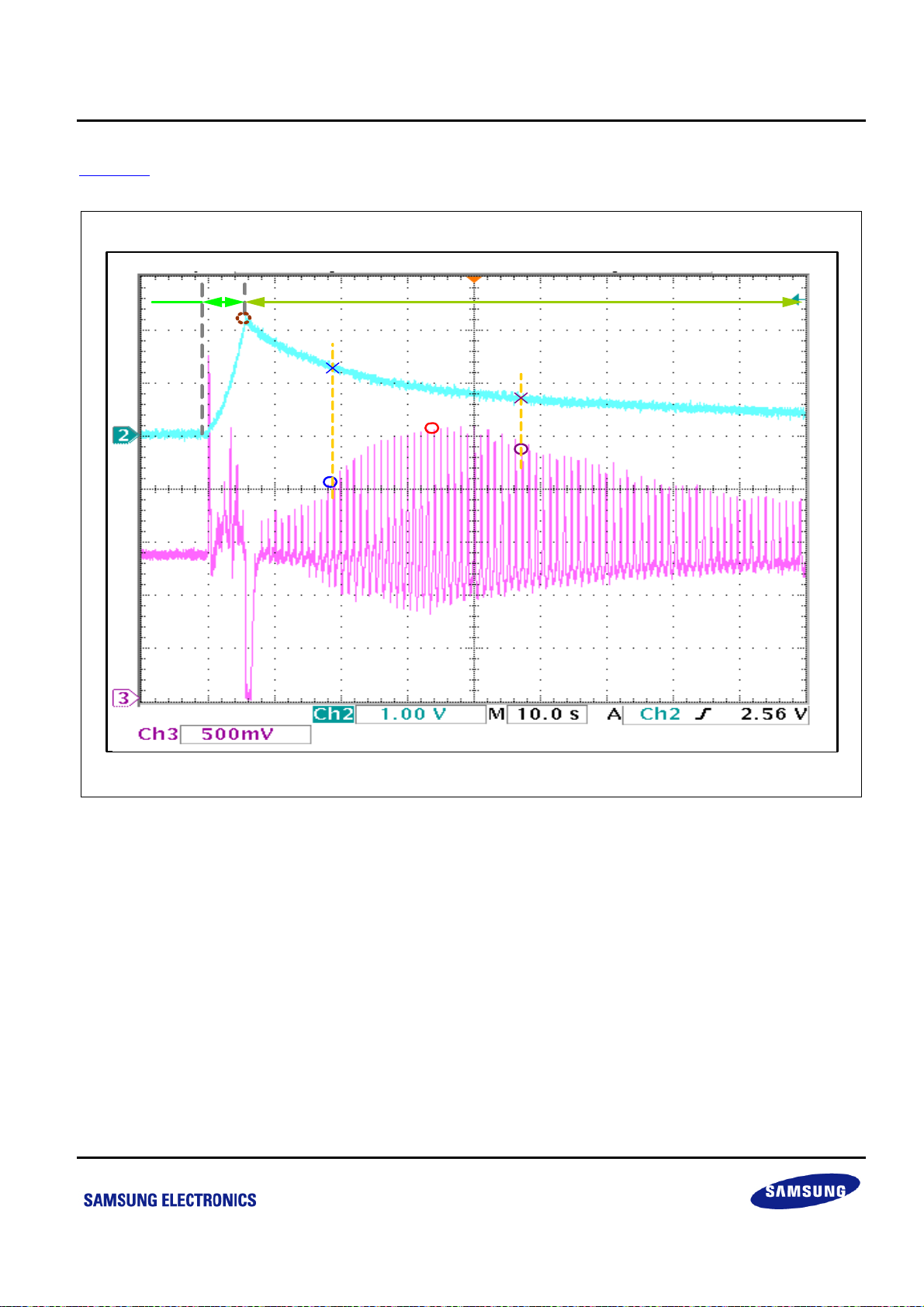
4 SCHEMATIC
Figure 4-1 Schematic of Analog Board
42
Page 43

S3P8245_ARM BLOOD PRESSURE MONITOR_AN_REV 0.00 错误!未定义样式。 错误!未定义样式。
Figure 4-2 Schematic of Main Board
43
Page 44

S3P8245_ARM BLOOD PRESSURE MONITOR_AN_REV 0.00 错误!未定义样式。 错误!未定义样式。
5 PCB LAYOUT
Figure 5-1 Main Board and Analog Board PCB Assembly (Top Layer)
44
Page 45

S3P8245_ARM BLOOD PRESSURE MONITOR_AN_REV 0.00 错误!未定义样式。 错误!未定义样式。
Figure 5-2 Main Board and Analog Board PCB Assembly (Bottom Layer)
Figure 5-3 Main Board and Analog Board PCB (Top Layer)
45
Page 46

S3P8245_ARM BLOOD PRESSURE MONITOR_AN_REV 0.00 错误!未定义样式。 错误!未定义样式。
Figure 5-4 Main Board PCB (Bottom Layer)
46
Page 47

S3P8245_ARM BLOOD PRESSURE MONITOR_AN_REV 0.00 错误!未定义样式。 错误!未定义样式。
Layout Guide
1. ADC0 and ADC1 are extremely sensitive signals in the BPM system. Therefore, they should be protected by
using ground lines.
LCD Screen
Buzzer
EEPROM
Valve
Motor
MCU
GND
S3P8245
Pump
Motor
BPM Main Board
V2.1
User Button
Analog Board
Inferface
Managment
+6V
Power
Figure 5-5 Final Implementation of Blood Pressure Monitor (Main Board)
Analog Board Interface
BPM AB V1.0
CCS PS PRTDiff-AMPHPF AMP LPF
Note:
CCS: Constant Current Source; PS: Pressure Sensor
Diff-AMP: Differential Amplifier; AMP: 11x Amplifier
HPF: 0.8Hz High-pass Filter;
LPF: 38Hz Low-pass Filter; PRT: Pulse Rate Trigger
Figure 5-6 Final Implementation of Blood Pressure Monitor (Analog Board)
47
Page 48

S3P8245_ARM BLOOD PRESSURE MONITOR_AN_REV 0.00 错误!未定义样式。 错误!未定义样式。
6 MEASUREMENT
6.1 Test Environment
The test environment comprises the following:
• Power supply: +6V DC power or 4x AA batteries
• Temperature: 25℃
• Equipments:
− Agilent E3648A DC Power Supply (Optional)
− Tektronix TDS3034B Digital Phosphor Oscilloscope
48
Page 49

S3P8245_ARM BLOOD PRESSURE MONITOR_AN_REV 0.00 错误!未定义样式。 错误!未定义样式。
6.2 Final Measurement Environment Setting
Figure 6-1 shows the final measurement environment setting of the BPM reference solution.
Cuff for Patient
Patient’s Arm
6V DC Valve Motor
6V DC Pump Motor
Main Board of BPM
Analog Board of BPM
4x AA Battery Power
Figure 6-1 Final Measurement Environment Setting
49
Page 50

S3P8245_ARM BLOOD PRESSURE MONITOR_AN_REV 0.00 错误!未定义样式。 错误!未定义样式。
6.3 Test Result
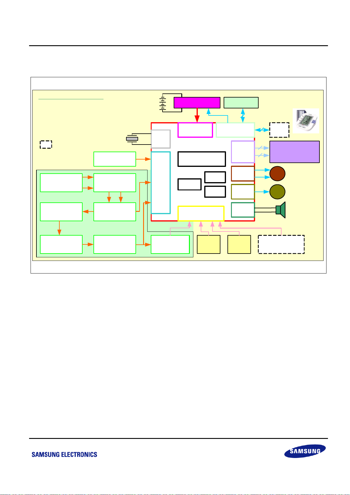
Figure 6-2 shows the real measurement of blood pressure waveform by using this BPM reference solution.
Pump Deflate
MAP
DBP
DC . BP
AC . BP
PR
SBP
Figure 6-2 Blood Pressure Signals Measurement Waveform
50
Page 51

S3P8245_ARM BLOOD PRESSURE MONITOR_AN_REV 0.00 错误!未定义样式。 错误!未定义样式。
7 APPENDIX 1: BILL OF MATERIALS
Table 7-1 Bill of Main Board Materials
Item Quantity Reference Value Comments
1 1 U2 4COM×19SEG LCD
2 1 U3 PCF8563 RTC, 8-SOP
3 1 U4 S3P8245 80-TQFP
4 1 U5 24C01 EEPROM, 8-SOP
5 1 U8 GM6155-5.0 SMD SOT-25
6 1 MG1 - 6V Pump Motor, 2-SIP
7 1 MG2 - 6V Valve Motor, 2-SIP
8 2 Y1, Y3 32.768 KHz Quartz crystal
9 1 Y2 10 MHz Quartz crystal
10 4 Q2, Q3, Q4, Q5 9012 SMD SOT-23
11 5 Q6, Q7, Q8, Q9, Q10 9013 SMD SOT-23
12 5 D1, D2, D3, D4, D6 1N4007 SMD DO-214AC
13 1 D5 LED SMD 1206
14 2 SW6, SW7 Button -
15 1 LS1 Buzzer -
16 1 J3 CON2 2-SIP
17 3 J5, J6, J7 CON2 Power Connector
18 1 J4 CON4 4-SIP
19 1 J8 CON3 3-SIP
20 1 J9 CON6 6-SIP
21 1 C5 Variable CAP 2-DIP
22 12
23 4 C7, C11, C15, C16 33pF SMD 0805
24 1 C9 CAP 2-DIP
25 2 C10, C28 100uF/10V SMD Tantalum Capacitor
26 2 C13, C23 10uF/10V SMD Tantalum Capacitor
27 1 C14 0.01uF SMD 0805
28 1 C19 47uF/10V SMD Tantalum Capacitor
29 1 C22 470uF/16V Aluminum Capacitor
C6, C8, C12, C17, C18, C20, C21,
C24, C25, C26, C27, C29
0.1uF SMD 0805
51
Page 52

S3P8245_ARM BLOOD PRESSURE MONITOR_AN_REV 0.00 错误!未定义样式。 错误!未定义样式。
30 4 R7, R11, R21, R22 20 KΩ SMD 0805
31 4 R10, R13, R14, R15 100 KΩ SMD 0805, 1%, 1/16 W, 50 V
32 1 R16 50 Ω SMD 0805, 1%, 1/16 W, 50 V
33 2 R17, R82 0 Ω SMD 0805, 1%, 1/16 W, 50 V
34 7
35 12
R18, R23, R24, R25, R40, R45,
R46
R19, R26, R28, R31, R32, R33,
R34, R35, R36, R38, R39, R42
10 KΩ SMD 0805
1 KΩ SMD 0805
36 2 R20, R41 100 Ω SMD 0805
37 2 R27, R43 0 Ω SMD 0805
38 1 R29 10 KΩ SMD 0805, 1%, 1/16 W, 50 V
39 1 R30 5.1 KΩ SMD 0805, 1%, 1/16 W, 50 V
40 1 R37 5.1 KΩ SMD 0805
52
Page 53

S3P8245_ARM BLOOD PRESSURE MONITOR_AN_REV 0.00 错误!未定义样式。 错误!未定义样式。
Table 7-2 Bill of Analog Board Materials
Item Quantity Reference Value Comments
1 1 U1
MPS-3117-
006G
Pressure Sensor, 6-SOP
2 2 U2, U4 LM358 8-SOP
3 1 U3 LM311 8-SOP
4 1 Q1 9012 SMD SOT-23
5 2 J1, J2 CON2 2-SIP
6 1 J3 CON6 6-SIP
7 1 J4 CON3 3-SIP
8 2 C1, C6 10uF/16V SMD Tantalum Capacitor
9 10
C2, C3, C4, C5, C7, C8, C9, C10,
C11, C12
0.1uF SMD 0805
10 2 R1, R2 4.7 KΩ SMD 0805
11 2 R3, R23 100 Ω SMD 0805, 1%, 1/16 W, 50 V
12 1 R4 1.2 KΩ SMD 0805, 1%, 1/16 W, 50 V
13 1 R5 0 KΩ SMD 0805, 1%, 1/16 W, 50 V
14 5 R6, R8, R13, R17, R35 1 MΩ SMD 0805, 1%, 1/16 W, 50 V
15 2 R7, R16 1.3 MΩ SMD 0805, 1%, 1/16 W, 50 V
16 2 R9, R10 200 KΩ SMD 0805, 1%, 1/16 W, 50 V
17 3 R11, R12, R29 30 KΩ SMD 0805, 1%, 1/16 W, 50 V
18 5 R14, R15, R25, R27, R30 1 KΩ SMD 0805, 1%, 1/16 W, 50 V
19 1 R18 1.5 MΩ SMD 0805, 1%, 1/16 W, 50 V
20 1 R19 360 KΩ SMD 0805, 1%, 1/16 W, 50 V
21 1 R20 2.4 KΩ SMD 0805, 1%, 1/16 W, 50 V
22 1 R21 182 KΩ SMD 0805, 1%, 1/16 W, 50 V
23 1 R22 100 KΩ SMD 0805, 1%, 1/16 W, 50 V
24 1 R24 50 KΩ
BOURNS3362 Single-Turn
Cermet Trimmers
25 1 R26 10 KΩ SMD 0805
26 2 R28, R32 10 KΩ SMD 0805, 1%, 1/16 W, 50 V
27 1 R31 49.9 KΩ SMD 0805, 1%, 1/16 W, 50 V
28 1 R33 5.1 MΩ SMD 0805, 1%, 1/16 W, 50 V
29 1 R34 10 MΩ SMD 0805, 1%, 1/16 W, 50 V
53
Page 54

S3P8245_ARM BLOOD PRESSURE MONITOR_AN_REV 0.00 错误!未定义样式。 错误!未定义样式。
8 APPENDIX 2: SOURCE CODE
For details on the source code, refer to the Arm_Blood_Pressure_Monitor_S3P8245_V1.2.rar.
54
 Loading...