

Samsung S3C80E5, S3C80E7, S3P80E5, S3P80E7 Datasheet

S3C80E5/P80E5/C80E7/P80E7 (Preliminary Spec) PRODUCT OVERVIEW
1 PRODUCT OVERVIEW
S3C8-SERIES MICROCONTROLLERS
Samsung's S3C8-series of 8-bit single-chip CMOS microcontrollers offers a fast and efficient CPU, a wide range
of integrated peripherals and various mask-programmable ROM sizes. Important CPU features include:
— Efficient register-oriented architecture
— Selectable CPU clock sources
— Idle and Stop power-down mode release by interrupt
— Built-in basic timer with watchdog function
A sophisticated interrupt structure recognizes up to eight interrupt levels. Each level can have one or more
interrupt sources and vectors. Fast interrupt processing (within a minimum six CPU clocks) can be assigned to
specific interrupt levels.
S3C80E5/C80E7 MICROCONTROLLER
The S3C80E5/C80E7 single-chip CMOS
microcontroller is fabricated using a highly
advanced CMOS process, based on Samsung’s
newest CPU architecture.
The S3C80E5/C80E7 is the microcontroller which
has 16/24-Kbyte mask-programmable ROM. The
S3P80E5/P80E7 is the microcontroller which has
16/24-Kbyte one-time-programmable EPROM.
Using a proven modular design approach, Samsung
engineers developed the S3C80E5/C80E7 by
integrating the following peripheral modules with the
powerful SAM87 core:
— Four programmable I/O ports, including three
8-bit ports and one 2-bit port, for a total of 26
pins.
— Internal LVD circuit and twelve bit-
programmable pins for external interrupts.
— One 8-bit basic timer for oscillation stabilization
and watchdog functions (system reset).
— One 8-bit timer/counter and one 16-bit
timer/counter with selectable operating modes.
— One 8-bit counter with auto-reload function and
one-shot or repeat control.
The S3C80E5/C80E7 is a versatile general-purpose
microcontroller which is especially suitable for use
as unified remote transmitter controller. It is
currently available in a 32-pin SOP and SDIP
package for S3C80E5 and S3C80E7. And available
in 40 DIP package only for S3C80E7.
OTP
The S3P80E5/P80E7 is an OTP (One Time Programmable) version of the S3C80E5/C80E7 microcontroller. The
S3P80E5/P80E7 microcontroller has an on-chip 16/24-Kbyte one-time-programmable EPROM instead of a
masked ROM. The S3P80E5/P80E7 is comparable to the S3C80E5/C80E7, both in function and in pin
configuration.
1-1

PRODUCT OVERVIEW S3C80E5/P80E5/C80E7/P80E7 (Preliminary Spec)
FEATURES
CPU
• SAM87 CPU core
Memory
• 16-Kbyte internal program memory (ROM):
S3C80E5
• 24-Kbyte internal program memory (ROM):
S3C80E7
• 256-byte internal (RAM): 8000–80FFH
• Data memory: 317-byte internal register file
Instruction Set
• 78 instructions
• IDLE and STOP instructions added for powerdown modes
Instruction Execution Time
• 750 ns at 8 MHz f
(minimum)
OSC
Interrupts
• Six interrupt levels and 18 interrupt sources
Carrier Frequency Generator
• One 8-bit counter with auto-reload function and
one-shot or repeat control (Counter A)
Back-up mode
• When reset pin is low level or when VDD is lower
than V
, the chip enters back-up mode to
LVD
reduce current consumption.
Low Voltage Detect Circuit
• Low voltage detect for reset or back-up mode
input.
• Low level detect voltage :
2.2 V (Typ) –100 mV/+ 200 mV
Operating Temperature Range
• – 40°C to + 85 °C
Operating Voltage Range
• 2.0 V to 5.5 V at 4 MHz f
• 2.1 V to 5.5 V at 8 MHz f
OSC
OSC
• 15 vectors (14 sources have a dedicated vector
address and four sources share a single vector)
• Fast interrupt processing feature (for one
selected interrupt level)
I/O Ports
• Three 8-bit I/O ports (P0–P2) and one 2-bit port
(P3) for a total of 26 bit-programmable pins
• Twelve input pins for external interrupts
Timers and Timer/Counters
• One programmable 8-bit basic timer (BT) for
oscillation stabilization control or watchdog timer
(software reset) function
• One 8-bit timer/counter (Timer 0) with three
operating modes; Interval, Capture, and PWM
• One 16-bit timer/counter (Timer 1) with two
operating modes; Interval and Capture
Package Type
• 32-pin SOP
• 32-pin SDIP
• 40-pin DIP
1-2
S3C80E5/P80E5/C80E7/P80E7 (Preliminary Spec) PRODUCT OVERVIEW
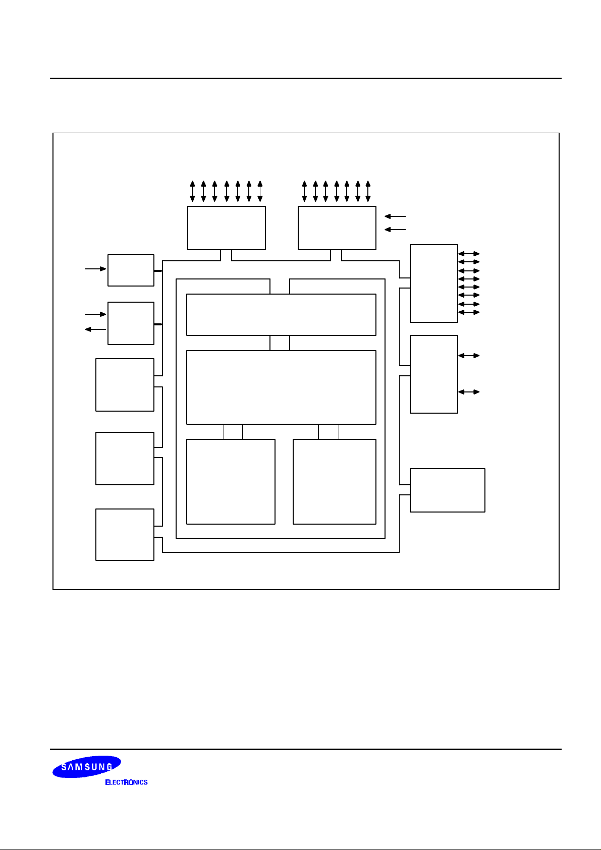
BLOCK DIAGRAM
P0.0–P0.7
(INT0–INT4)
PORT 0
P1.0–P1.7
PORT 1
RESET
TEST
V
X
DD
X
IN
OUT
LVD
MAIN
OSC
8-BIT
BASIC
TIMER
8-BIT
TIMER/
COUNTER
16-BIT
TIMER/
COUNTER
INTERNAL BUS
I/O PORT and INTERRUPT
CONTROL
SAM87
CPU
PROGRAM
MEMORY
(16/24-Kbyte Program
Memory and 256-Byte
Program RAM)
317-BYTE
REGISTER
FILE
PORT2
PORT 3
CARRIER
GENERATOR
(COUNTER A)
P2.0–P2.3
(INT5–INT8)
P2.4–P2.7
P3.0/T0PWM/
T0CAP/T1CAP
P3.1/REM/T0CK
Figure 1-1. Block Diagram
1-3
PRODUCT OVERVIEW S3C80E5/P80E5/C80E7/P80E7 (Preliminary Spec)
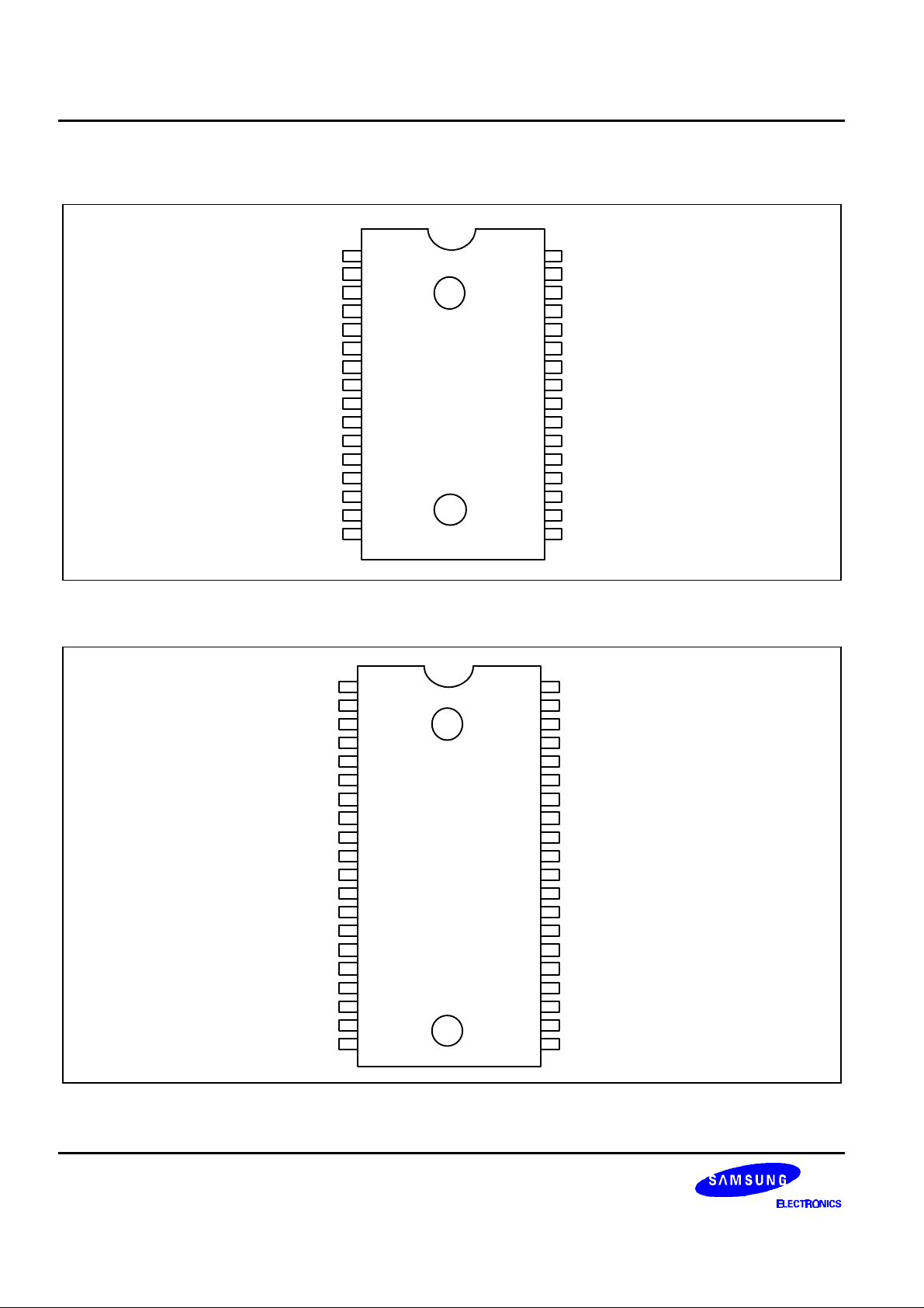
PIN ASSIGNMENTS
V
SS
X
X
OUT
TEST
P2.0/INT5
P2.1/INT6
P2.2/INT7
P2.3/INT8
P0.0/INT0
P0.1/INT1
P0.2/INT2
P0.3/INT3
P0.4/INT4
P0.5/INT4
P0.6/INT4
P0.7/INT4
IN
1
2
3
4
5
6
S3C80E5
7
S3C80E7
8
32-SOP/SDIP
9
10
(Top View)
11
12
13
14
15
16
32
31
30
29
28
27
26
25
24
23
22
21
20
19
18
17
V
DD
RESET/BACK-UP MODE
P3.1/REM/T0CK
P3.0/T0PWM/T0CAP/T1CAP
P2.7
P2.6
P2.5
P2.4
P1.7
P1.6
P1.5
P1.4
P1.3
P1.2
P1.1
P1.0
Figure 1-2. Pin Assignment (32-Pin SOP/SDIP Package)
V
SS
X
X
OUT
TEST
NC
NC
P2.0/INT5
P2.1/INT6
P2.2/INT7
P2.3/INT8
P0.0/INT0
P0.1/INT1
P0.2/INT2
P0.3/INT3
NC
NC
P0.4/INT4
P0.5/INT4
P0.6/INT4
P0.7/INT4
1
IN
2
3
4
5
6
7
8
S3C80E5
9
S3C80E7
10
11
40-DIP
12
(Top View)
13
14
15
16
17
18
19
20
40
39
38
37
36
35
34
33
32
31
30
29
28
27
26
25
24
23
22
21
V
DD
RESET/BACK-UP MODE
P3.1/REM/T0CK
P3.0/T0PWM/T0CAP/T1CAP
NC
NC
P2.7
P2.6
P2.5
P2.4
P1.7
P1.6
P1.5
P1.4
NC
NC
P1.3
P1.2
P1.1
P1.0
1-4
Figure 1-3. Pin Assignment (40-Pin DIP Package)
S3C80E5/P80E5/C80E7/P80E7 (Preliminary Spec) PRODUCT OVERVIEW
Table 1-1. Pin Descriptions
Pin
Names
Pin
Type
Pin
Description
P0.0–P0.7 I/O I/O port with bit-programmable pins.
Configurable to input or push-pull output
mode. Pull-up resistors are assignable by
software. Pins can be assigned individually
as external interrupt inputs with noise filters,
interrupt enable/disable, and interrupt
pending control.
P1.0–P1.7 I/O I/O port with bit-programmable pins.
Configurable to C-MOS input mode or
output mode. Pin circuits are either pushpull or n-channel open-drain type. Pull-up
resistors are assignable by software.
P2.0–P2.3
P2.4–P2.7
I/O General-purpose I/O port with bit-
programmable pins. Configurable to CMOS input mode, push-pull output mode, or
n-channel open-drain output mode. Pull-up
resistors are assignable by software. Lower
nibble pins, P2.3–P2.0, can be assigned as
external interrupt inputs with noise filters,
interrupt enable/disable, and interrupt
pending control.
Circuit
Type
1 9–16
2 17–24
3
4
Pin No.
(32-pin)
5–8,
25–28
Pin No.
(40-pin)
11–14,
17–20
21–24,
27–30
7–10,
31–34
Shared
Functions
INT0–INT4
–
INT5–INT8
–
P3.0
P3.1
I/O 2-bit I/O port with bit-programmable pins.
Configurable to C-MOS input mode, pushpull output mode, or n-channel open-drain
output mode. Pull-up resistors are
assignable by software. The two port 3 pins
have high current drive capability.
XIN, X
OUT
RESET/
BACK-UP
MODE
– System clock input and output pins – 2, 3 2, 3 –
I System reset signal input pin and back-up
mode input pin. The pin circuit is a C-MOS
input.
TEST I Test signal input pin (for factory use only;
must be connected to VSS).
V
DD
V
SS
– Power supply input pin – 32 40 –
– Ground pin – 1 1 –
5 29
30
37
38
T0PWM/
T0CAP/
T1CAP/
REM/T0CK
6 31 39 –
– 4 4 –
1-5

PRODUCT OVERVIEW S3C80E5/P80E5/C80E7/P80E7 (Preliminary Spec)
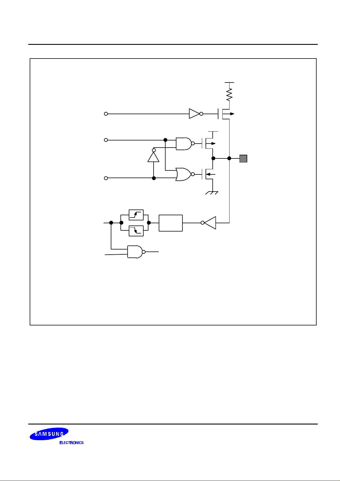
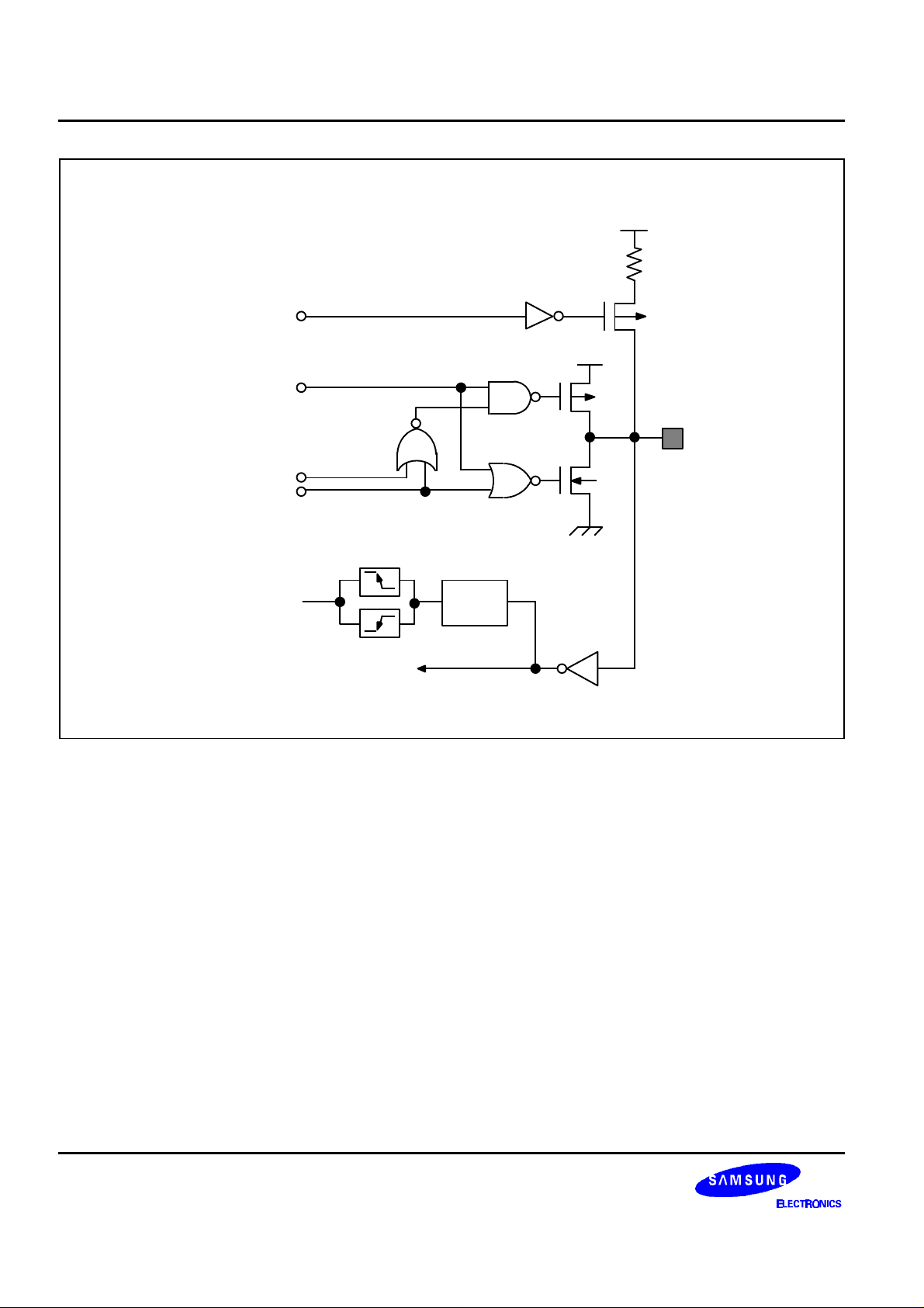
PIN CIRCUITS
V
DD
PULL-UP RESISTOR
(Typical 21 KΩ)
PULL-UP
ENABLE
V
DD
DATA
I/O
OUTPUT
DISABLE
INTERRUPT INPUT
IRQ6,7 (INT0-4)
NOTE:
To prevent and recover from abnormal stop status caused by battery bouncing, the S3P80E5
has a special logic_
input/output of universal remote controller. When these ports (P0, P1) are used as a normal
input pin, unexpected stop mode recovery can occur by input level switching. Hence, the user
should be aware of input level switching, if P0 and P1 are to be used as normal input ports.
STOP
V
NOISE
FILTER
NORMAL
INPUT
Oscillator Release (SED and R circuit)
SED and R circuit−related to P0 and P1. This is a specific function for key
SS
Figure 1-4. Pin Circuit Type 1 (Port 0)
1-6
S3C80E5/P80E5/C80E7/P80E7 (Preliminary Spec) PRODUCT OVERVIEW
V
DD
PULL-UP RESISTOR
(Typical 21 KΩ)
PULL-UP
ENABLE
V
DD
DATA
I/O
OUTPUT
DISABLE
V
SS
NOTE:
NORMAL INPUT
STOP
NOISE
FILTER
Oscillator Release (SED and R circuit)
To prevent and recover from abnormal stop status caused by battery bouncing, the S3P80E5
has a special logic
SED and R circuit−related to P0 and P1. This is a specific function for key
−
input/output of universal remote controller. When these ports (P0, P1) are used as a normal
input pin, unexpected stop mode releasing can occur by input level switching. Hence, the user
should be aware of input level switching, if P0 and P1 are to be used as normal input ports.
Figure 1-5. Pin Circuit Type 2 (Port 1)
1-7
PRODUCT OVERVIEW S3C80E5/P80E5/C80E7/P80E7 (Preliminary Spec)
V
DD
PULL-UP RESISTOR
(Typical 21 KΩ)
PULL-UP
ENABLE
V
DD
DATA
I/O
OPEN-DRAIN
OUTPUT
DISABLE
V
SS
EXTERNAL
INTERRUPT
IRQ5 (INT5-8)
NOISE
FILTER
NORMAL INPUT
Figure 1-6. Pin Circuit Type 3 (Ports 2.0–2.3)
1-8

S3C80E5/P80E5/C80E7/P80E7 (Preliminary Spec) PRODUCT OVERVIEW
V
DD
PULL-UP RESISTOR
(Typical 21 KΩ)
PULL-UP
ENABLE
V
DD
DATA
I/O
OPEN-DRAIN
OUTPUT
DISABLE
V
SS
NORMAL INPUT
Figure 1-7. Pin Circuit Type 4 (P2.4−−P2.7)
1-9

PRODUCT OVERVIEW S3C80E5/P80E5/C80E7/P80E7 (Preliminary Spec)
V
DD
PULL-UP RESISTOR
(Typical 21 KΩ)
PULL-UP
ENABLE
PORT 3 DATA
SELECT
M
DATA
V
DD
U
ALTERNATIVE
X
OUTPUT
I/O
OPEN-DRAIN
OUTPUT
DISABLE
NORMAL INPUT
ALTERNATIVE
INPUT
RESET/
BACK-UP
MODE
Figure 1-9. Pin Circuit Type 6 (RESETRESET/BACK-UP MODEBACK-UP MODE)
NOISE
FILTER
Figure 1-8. Pin Circuit Type 5 (P 3)
NOISE
FILTER
V
SS
BACK-UP MODE
SYSTEM
RESET
1-10
 Loading...