

Page 1

USER’S MANUAL
S3F80P5X
S3F80P5 MICROCONTROLLERS
April 2010
REV 1.00
Confidential Proprietary of Samsung Electronics Co., Ltd
Copyright © 2009 Samsung Electronics, Inc. All Rights Reserved
Page 2

Important Notice
The information in this publication has been carefully
checked and is believed to be entirely accurate at
the time of publication. Samsung assumes no
responsibility, however, for possible errors or
omissions, or for any consequences resulting from
the use of the information contained herein.
Samsung reserves the right to make changes in its
products or product specifications with the intent to
improve function or design at any time and without
notice and is not required to update this
documentation to reflect such changes.
This publication does not convey to a purchaser of
semiconductor devices described herein any license
under the patent rights of Samsung or others.
Samsung makes no warranty, representation, or
guarantee regarding the suitability of its products for
any particular purpose, nor does Samsung assume
any liability arising out of the application or use of
any product or circuit and specifically disclaims any
and all liability, including without limitation any
consequential or incidental damages.
S3F80P5 Microcontroller
User's Manual, Revision 1.00
"Typical" parameters can and do vary in different
applications. All operating parameters, including
"Typicals" must be validated for each customer
application by the customer's technical experts.
Samsung products are not designed, intended, or
authorized for use as components in systems
intended for surgical implant into the body, for other
applications intended to support or sustain life, or for
any other application in which the failure of the
Samsung product could create a situation where
personal injury or death may occur.
Should the Buyer purchase or use a Samsung
product for any such unintended or unauthorized
application, the Buyer shall indemnify and hold
Samsung and its officers, employees, subsidiaries,
affiliates, and distributors harmless against all
claims, costs, damages, expenses, and reasonable
attorney fees arising out of, either directly or
indirectly, any claim of personal injury or death that
may be associated with such unintended or
unauthorized use, even if such claim alleges that
Samsung was negligent regarding the design or
manufacture of said product.
Publication Number: S3-F80P5-022009
Copyright © 2009 Samsung Electronics Co., Ltd.
All rights reserved. No part of this publication may be reproduced, stored in a retrieval system, or transmitted in
any form or by any means, electric or mechanical, by photocopying, recording, or otherwise, without the prior
written consent of Samsung Electronics.
Samsung Electronics' microcontroller business has been awarded full ISO-14001
certification (BSI Certificate No. FM24653). All semiconductor products are
designed and manufactured in accordance with the highest quality standards and
objectives.
Samsung Electronics Co., Ltd.
San #24 Nongseo-Dong, Giheung-Gu
Yongin-City, Gyeonggi-Do, Korea
C.P.O. Box #37, Suwon 446-711
TEL: (82)-(31)-209-3865
FAX: (82)-(31)-209-6494
Home Page: http://www.samsungsemi.com
Printed in the Republic of Korea
Page 3

Preface
The S3F80P5 Microcontroller User's Manual is designed for application designers and programmers who are
using the S3F80P5 microcontroller for application development. It is organized in two main parts:
Part I Programming Model Part II Hardware Descriptions
Part I contains software-related information to familiarize you with the microcontroller's architecture, programming
model, and address spaces. It has three chapters:
Chapter 1 Product Overview
Chapter 2 Address Spaces
Chapter 1, "Product Overview," is a high-level introduction to S3F80P5 with general product descriptions, as well
as detailed information about individual pin characteristics and pin circuit types.
Chapter 2, “Address Spaces,” describes the important feature of the S3F80P5 programming environment.
Chapter 3, "Addressing Modes," describes program and data memory spaces, the internal register file, and
register addressing.
Chapter 4, “Control Registers,” describes the definition, usages and supported APIs for Flash operations.
A basic familiarity with the information in Part I will help you to understand the hardware module descriptions in
Part II. If you are not yet familiar with the S3FS-series microcontroller family and are reading this manual for the
first time, we recommend that you first read Chapters 1-3 carefully. Then, you can reference the information in
Part II as necessary.
Part II "hardware Descriptions," has detailed information about specific hardware components of the S3F80P5
microcontroller. Also included in Part II is electrical data. It has 15 chapters:
Chapter 5 Interrupt Structure
Chapter 6 Instruction Set
Chapter 7 Clock and Power Circuits
Chapter 8 Reset
Chapter 9 I/O Ports
Chapter 10 Basic Timer and Timer 0
Chapter 11 Timer 1
Chapter 12 Counter A
Two order forms are included at the back of this manual to facilitate customer order for S3F80P5 microcontroller:
the Mask ROM Order Form, and the Mask Option Selection Form.
You can photocopy these forms, fill them out, and then forward them to your local Samsung Sales
Representative.
Chapter 3 Addressing Modes
Chapter 4 Control Registers
Chapter 13 Timer 2
Chapter 14 Embedded Flash Memory Interface
Chapter 15 Low Voltage Detector
Chapter 16 Electrical Data
Chapter 17 Mechanical Data
Chapter 18 S3F80P5 Flash MCU
Chapter 19 Development Tools
S3F80P5_UM_REV1.00 MICROCONTROLLER iii
Page 4

Table of Contents
Part I — Programming Model
Chapter 1 Product Overview
S3C8/S3F8-Series Microcontrollers..............................................................................................................1-1
S3F80P5 Microcontroller...............................................................................................................................1-1
Features ........................................................................................................................................................1-2
CPU.........................................................................................................................................................1-2
Memory...................................................................................................................................................1-2
Instruction Set.........................................................................................................................................1-2
Instruction Execution Time .....................................................................................................................1-2
Interrupts.................................................................................................................................................1-2
I/O Ports..................................................................................................................................................1-2
Carrier Frequency Generator..................................................................................................................1-2
Basic Timer and Timer/Counters............................................................................................................1-2
Back-up Mode.........................................................................................................................................1-2
Low Voltage Detect Circuit .....................................................................................................................1-2
Operating Temperature Range...............................................................................................................1-2
Operating Voltage Range .......................................................................................................................1-2
Package Types.......................................................................................................................................1-2
Block Diagram (24-pin package)...................................................................................................................1-3
Pin Assignments............................................................................................................................................1-4
Pin Circuits ....................................................................................................................................................1-6
Chapter 2 Address Spaces
Overview........................................................................................................................................................2-1
Program Memory...........................................................................................................................................2-2
Smart Option...........................................................................................................................................2-3
Register Architecture.....................................................................................................................................2-5
Register Page Pointer (PP) ....................................................................................................................2-7
Register Set 1.........................................................................................................................................2-8
Register Set 2.........................................................................................................................................2-8
Prime Register Space.............................................................................................................................2-9
Working Registers...................................................................................................................................2-10
Using the Register Pointers....................................................................................................................2-11
Register Addressing......................................................................................................................................2-13
Common Working Register Area (C0H–CFH)........................................................................................2-15
Example 1:..............................................................................................................................................2-16
Example 2:..............................................................................................................................................2-16
4-Bit Working Register Addressing.........................................................................................................2-16
8-Bit Working Register Addressing.........................................................................................................2-18
System and User Stacks...............................................................................................................................2-20
Stack Operations ....................................................................................................................................2-20
User-Defined Stacks...............................................................................................................................2-20
Stack Pointers (SPL)...............................................................................................................................2-20
iv S3F80P5_UM_REV 1.00 MICROCONTROLLER
Page 5

Table of Contents (Continued)
Chapter 3 Addressing Modes
Overview .......................................................................................................................................................3-1
Register Addressing Mode (R)...............................................................................................................3-2
Indirect Register Addressing Mode (IR).................................................................................................3-3
Indexed Addressing Mode (X)................................................................................................................3-7
Direct Address Mode (DA) .....................................................................................................................3-10
Direct Address MODE (Continued)........................................................................................................3-11
Indirect Address Mode (IA).....................................................................................................................3-12
Relative Address Mode (RA)..................................................................................................................3-13
Immediate Mode (IM) .............................................................................................................................3-14
Chapter 4 Control Registers
Overview .......................................................................................................................................................4-1
Chapter 5 Interrupt Structure
Overview .......................................................................................................................................................5-1
Levels .....................................................................................................................................................5-1
Vectors....................................................................................................................................................5-1
Sources...................................................................................................................................................5-1
Interrupt Types .......................................................................................................................................5-2
Interrupt Vector Addresses.....................................................................................................................5-4
Enable/Disable Interrupt Instructions (EI, DI).........................................................................................5-6
System-Level Interrupt Control Registers ..............................................................................................5-6
Interrupt Processing Control Points........................................................................................................5-7
Peripheral Interrupt Control Registers....................................................................................................5-8
System Mode Register (SYM)................................................................................................................5-9
Interrupt Mask Register (IMR)................................................................................................................5-10
Interrupt Priority Register (IPR)..............................................................................................................5-11
Interrupt Request Register (IRQ) ...........................................................................................................5-13
Interrupt Pending Function Types..........................................................................................................5-14
Overview.................................................................................................................................................5-14
Pending Bits Cleared Automatically by Hardware..................................................................................5-14
Pending Bits Cleared by the Service Routine ........................................................................................5-14
Interrupt Source Polling Sequence.........................................................................................................5-15
Interrupt Service Routines......................................................................................................................5-15
Generating interrupt Vector Addresses..................................................................................................5-16
Nesting of Vectored Interrupts................................................................................................................5-16
Instruction Pointer (IP)............................................................................................................................5-16
Fast Interrupt Processing .......................................................................................................................5-16
Fast Interrupt Processing (Continued) ...................................................................................................5-17
Procedure for Initiating Fast Interrupt.....................................................................................................5-17
Fast Interrupt Service Routine................................................................................................................5-17
Programming Guidelines........................................................................................................................5-17
S3F80P5_UM_REV1.00 MICROCONTROLLER v
Page 6

Table of Contents(Continued)
Chapter 6 Instruction Set
Overview........................................................................................................................................................6-1
Data Types..............................................................................................................................................6-1
Register Addressing................................................................................................................................6-1
Addressing Modes..................................................................................................................................6-1
Flags Register (FLAGS) .........................................................................................................................6-6
Flag Descriptions....................................................................................................................................6-7
Instruction Set Notation...........................................................................................................................6-8
Condition Codes .....................................................................................................................................6-12
Instruction Descriptions ..........................................................................................................................6-13
Chapter 7 Clock and Power Circuit
Overview........................................................................................................................................................7-1
System Clock Circuit...............................................................................................................................7-1
Clock Status During Power-Down Modes ..............................................................................................7-3
System Clock Control Register (CLKCON)............................................................................................7-4
Chapter 8 RESET
Overview........................................................................................................................................................8-1
Reset Sources ........................................................................................................................................8-1
Reset Mechanism...................................................................................................................................8-4
Watch dog timer Reset ...........................................................................................................................8-4
LVD Reset...............................................................................................................................................8-4
Internal Power-On Reset ........................................................................................................................8-5
External Interrupt Reset..........................................................................................................................8-6
Stop Error Detection & Recovery............................................................................................................8-7
Power-Down Modes......................................................................................................................................8-8
Idle Mode ................................................................................................................................................8-8
IDLE Mode Release................................................................................................................................8-8
Back-up Mode.........................................................................................................................................8-9
Stop Mode...............................................................................................................................................8-11
Sources to Release Stop Mode..............................................................................................................8-12
Using IPOR to Release Stop Mode........................................................................................................8-12
Using an External Interrupt to Release Stop Mode................................................................................8-12
SED&R (Stop Error Detect and Recovery).............................................................................................8-13
System Reset Operation.........................................................................................................................8-14
Hardware Reset Values..........................................................................................................................8-15
Recommendation for Unusued Pins.......................................................................................................8-19
Summary Table of Back-up Mode, Stop Mode, and Reset Status.........................................................8-20
vi S3F80P5_UM_REV 1.00 MICROCONTROLLER
Page 7

Table of Contents (Continued)
Part II
Hardware Descriptions
Chapter 9 I/O Ports
Overview .......................................................................................................................................................9-1
Port Data Registers................................................................................................................................9-3
Pull-Up Resistor Enable Registers.........................................................................................................9-4
Chapter 10 Basic timer and Timer 0
Overview .......................................................................................................................................................10-1
Basic Timer (BT).....................................................................................................................................101
Timer 0....................................................................................................................................................10-1
Basic Timer Control Register (BTCON) .................................................................................................10-2
Basic Timer Function Description...........................................................................................................10-3
Watch-dog Timer Function.....................................................................................................................10-3
Oscillation Stabilization Interval Timer Function ....................................................................................10-3
Timer 0 Control Register (T0CON).........................................................................................................10-4
Timer 0 Function Description .................................................................................................................10-6
Timer 0 Interrupts (IRQ0, Vectors FAH and FCH).................................................................................10-6
Interval Timer Mode................................................................................................................................10-6
Pulse Width Modulation Mode................................................................................................................10-7
Capture Mode.........................................................................................................................................10-8
Chapter 11 Timer 1
Overview .......................................................................................................................................................11-1
Timer 1 Overflow Interrupt ......................................................................................................................11-2
Timer 1 Capture Interrupt.......................................................................................................................11-2
Timer 1 Match Interrupt..........................................................................................................................11-3
Timer 1 Control Register (T1CON).........................................................................................................11-5
S3F80P5_UM_REV1.00 MICROCONTROLLER vii
Page 8

Table of Contents (Continued)
Chapter 12 Counter A
Overview........................................................................................................................................................12-1
Counter A Control Register (CACON)....................................................................................................12-3
Counter A Pulse Width Calculations.......................................................................................................12-4
Chapter 13 Timer 2
Overview........................................................................................................................................................13-1
Timer 2 Overflow Interrupt......................................................................................................................13-2
Timer 2 Capture Interrupt .......................................................................................................................13-2
Timer 2 Match Interrupt...........................................................................................................................13-3
Timer 2 Control Register (T2CON).........................................................................................................13-5
Chapter 14 Embedded Flash Memory Interface
Overview........................................................................................................................................................14-1
Flash ROM Configuration.......................................................................................................................14-1
User Program Mode................................................................................................................................14-2
ISPTM (On-Board Programming) SECTOR..................................................................................................14-2
Smart Option...........................................................................................................................................14-3
ISP Reset Vector and ISP Sector Size...................................................................................................14-4
Flash Memory Control Registers (User Program Mode)...............................................................................14-5
Flash Memory Control Register (FMCOn)..............................................................................................14-5
Flash Memory User Programming Enable Register (FMUSR)...............................................................14-5
Flash Memory Sector Address Registers...............................................................................................14-6
Sector Erase..................................................................................................................................................14-7
The Sector Erase Procedure in User Program Mode.............................................................................14-8
Programming.................................................................................................................................................14-11
The Program Procedure in User Program Mode....................................................................................14-11
Reading.........................................................................................................................................................14-16
The Program Procedure in User Program Mode....................................................................................14-16
Hard Lock Protection.....................................................................................................................................14-17
The Program Procedure in User Program Mode....................................................................................14-17
viii S3F80P5_UM_REV 1.00 MICROCONTROLLER
Page 9

Table of Contents (Conclude)
Chapter 15 Lower Voltage Detector
Overview .......................................................................................................................................................15-1
LVD.........................................................................................................................................................15-1
LVD FLAG ..............................................................................................................................................15-1
Low Voltage Detector Control Register (LVDCON) ...............................................................................15-4
Low Voltage Detector Flag Selection Register (LVDSEL) .....................................................................15-4
Chapter 16 Electrical Data
16.1 Overview...............................................................................................................................................16-1
Chapter 17 Mechanical
17.1 Overview...............................................................................................................................................17-1
Chapter 18 S3F80P5 Flash MCU
Overview .......................................................................................................................................................18-1
Operating Mode Characteristics.............................................................................................................18-4
Chapter 19 Development Tools
Overview .......................................................................................................................................................19-1
Target Boards...........................................................................................................................................19-1
Programming Socket Adapter ..................................................................................................................19-1
TB80PB Target Board ..............................................................................................................................19-3
Third Parties for Development Tools....................................................................................................19-7
In-Circuit Emulator for SAM8 Family....................................................................................................19-7
OTP/MTP Programmer ........................................................................................................................19-7
Development Tools Suppliers ..............................................................................................................19-7
8-bit In-Circuit Emulator........................................................................................................................19-7
OTP/MTP Programmer (Writer)................................................................................................................19-8
S3F80P5_UM_REV1.00 MICROCONTROLLER ix
Page 10

Page 11

List of Figures
Figure Title Page
Number Number
1-1 Block Diagram (24-pin)..............................................................................................1-3
1-2 Pin Assignment Diagram (24-Pin SOP/SDIP Package) ............................................1-4
1-3 Pin Circuit Type 1 (Port 0)..........................................................................................1-6
1-4 Pin Circuit Type 2 (Port 1)..........................................................................................1-7
1-5 Pin Circuit Type 2 (Port 2)..........................................................................................1-8
1-6 Pin Circuit Type 4 (P3.0)............................................................................................1-9
1-7 Pin Circuit Type 5 (P3.1)............................................................................................1-10
2-1 Program Memory Address Space..............................................................................2-2
2-2 Smart Option ..............................................................................................................2-3
2-3 Internal Register File Organization.............................................................................2-6
2-4 Register Page Pointer (PP)........................................................................................2-7
2-5 Set 1, Set 2, and Prime Area Register Map...............................................................2-9
2-6 8-Byte Working Register Areas (Slices).....................................................................2-10
2-7 Contiguous 16-Byte Working Register Block.............................................................2-11
2-8 Non-Contiguous 16-Byte Working Register Block.....................................................2-12
2-9 16-Bit Register Pair....................................................................................................2-13
2-10 Register File Addressing............................................................................................2-14
2-11 Common Working Register Area ...............................................................................2-15
2-12 4-Bit Working Register Addressing............................................................................2-17
2-13 4-Bit Working Register Addressing Example.............................................................2-17
2-14 8-Bit Working Register Addressing............................................................................2-18
2-15 8-Bit Working Register Addressing Example.............................................................2-19
2-16 Stack Operations........................................................................................................2
3-1 Register Addressing...................................................................................................3-2
3-2 Working Register Addressing.....................................................................................3-2
3-3 Indirect Register Addressing to Register File.............................................................3-3
3-4 Indirect Register Addressing to Program Memory.....................................................3-4
3-5 Indirect Working Register Addressing to Register File ..............................................3-5
3-6 Indirect Working Register Addressing to Program or Data Memory..........................3-6
3-7 Indexed Addressing to Register File..........................................................................3-7
3-8 Indexed Addressing to Program or Data Memory with Short Offset..........................3-8
3-9 Indexed Addressing to Program or Data Memory......................................................3-9
3-10 Direct Addressing for Load Instructions.....................................................................3-10
3-11 Direct Addressing for Call and Jump Instructions......................................................3-11
3-12 Indirect Addressing.....................................................................................................3-12
3-13 Relative Addressing ...................................................................................................3-13
3-14 Immediate Addressing................................................................................................3-14
4-1 Register Description Format ......................................................................................4-5
-20
S3F80P5_UM_REV1.00 MICROCONTROLLER xi
Page 12

List of Figures (Continued)
Figure Title Page
Number Number
5-1 S3C8/S3F8-Series Interrupt Types ............................................................................5-2
5-2 S3F80P5 Interrupt Structure.......................................................................................5-3
5-3 ROM Vector Address Area.........................................................................................5-4
5-4 Interrupt Function Diagram.........................................................................................5-7
5-5 System Mode Register (SYM)....................................................................................5-9
5-6 Interrupt Mask Register (IMR)....................................................................................5-10
5-7 Interrupt Request Priority Groups...............................................................................5-11
5-8 Interrupt Priority Register (IPR)..................................................................................5-12
5-9 Interrupt Request Register (IRQ) ...............................................................................5-13
6-1 System Flags Register (FLAGS)................................................................................6-6
7-1 Main Oscillator Circuit (External Crystal or Ceramic Resonator) ............................7-2
7-2 External Clock Circuit .................................................................................................7-2
7-3 System Clock Circuit Diagram....................................................................................7-3
7-4 System Clock Control Register (CLKCON)................................................................7-4
7-5 Power Circuit (VDD) ...................................................................................................7-5
7-6 Guide Line of Chip Operating Voltage........................................................................7-5
8-1 RESET Sources of the S3F80P5 ...............................................................................8-2
8-2 RESET Block Diagram of the S3F80P5.....................................................................8-3
8-3 RESET Block Diagram by LVD for the S3F80P5 in Stop Mode.................................8-4
8-4 Timing Diagram for Internal Power-On Reset Circuit.................................................8-5
8-5 Reset Timing Diagram for the S3F80P5 in Stop Mode by IPOR ...............................8-6
8-6 Block Diagram for Back-up Mode...............................................................................8-9
8-7 Timing Diagram for Back-up Mode Input and Released by LVD ...............................8-9
8-8 Timing Diagram for Back-up Mode Input in Stop Mode.............................................8-10
9-1 S3F80P5 I/O Port Data Register Format....................................................................9-3
9-2 Pull-up Resistor Enable Registers (Port 0 and Port2)................................................9-4
10-1 Basic Timer Control Register (BTCON) .....................................................................10-2
10-2 Timer 0 Control Register (T0CON).............................................................................10-5
10-3 Timer 0 DATA Register (T0DATA).............................................................................10-5
10-4 Simplified Timer 0 Function Diagram: Interval Timer Mode.......................................10-6
10-5 Simplified Timer 0 Function Diagram: PWM Mode ....................................................10-7
10-6 Simplified Timer 0 Function Diagram: Capture Mode................................................10-8
10-7 Basic Timer and Timer 0 Block Diagram....................................................................10-9
11-1 Simplified Timer 1 Function Diagram: Capture Mode................................................11-2
11-2 Simplified Timer 1 Function Diagram: Interval Timer Mode.......................................11-3
11-3 Timer 1 Block Diagram...............................................................................................11-4
11-4 Timer 1 Control Register (T1CON).............................................................................11-5
11-5 Timer 1 Registers (T1CNTH, T1CNTL, T1DATAH, T1DATAL) .................................11-6
xii S3F80P5_UM_REV1.00 MICROCONTROLLER
Page 13

List of Figures (Conclude)
Figure Title Page
Number Number
12-1 Counter A Block Diagram...........................................................................................12-2
12-2 Counter A Control Register (CACON) .......................................................................12-3
12-3 Counter A Registers...................................................................................................12-3
12-4 Counter A Output Flip-Flop Waveforms in Repeat Mode ..........................................12-5
13-1 Simplified Timer 2 Function Diagram: Capture Mode................................................13-2
13-2 Simplified Timer 2 Function Diagram: Interval Timer Mode.......................................13-3
13-3 Timer 2 Block Diagram...............................................................................................13-4
13-4 Timer 2 Control Register (T2CON) ............................................................................13-5
13-5 Timer 2 Registers (T2CNTH, T2CNTL, T2DATAH, T2DATAL).................................13-6
14-1 Program Memory Address Space..............................................................................14-2
14-2 Smart Option ..............................................................................................................14-3
14-3 Flash Memory Control Register (FMCON).................................................................14-5
14-4 Flash Memory User Programming Enable Register (FMUSR)..................................14-5
14-5 Flash Memory Sector Address Register (FMSECH) .................................................14-6
14-6 Flash Memory Sector Address Register (FMSECL)..................................................14-6
14-7 Sector Configurations in User Program Mode...........................................................14-7
14-8 Sector Erase Flowchart in User Program Mode ........................................................14-8
14-9 Byte Program Flowchart in a User Program Mode....................................................14-12
14-10 Program Flowchart in a User Program Mode............................................................14-13
15-1 Low Voltage Detect (LVD) Block Diagram.................................................................15-3
15-2 Low Voltage Detect Control Register (LVDCON) ......................................................15-4
15-3 Low Voltage Detect Flag Selection Register (LVDSEL) ............................................15-4
16-1 Stop Mode Release Timing When Initiated by an External Interrupt.........................16-6
16-2 Stop Mode Release Timing When Initiated by a LVD................................................16-7
16-3 Input Timing for External Interrupts (Port 0 and Port 2).............................................16-8
16-4 Operating Voltage Range of S3F80P5.......................................................................16-11
17-1 24-Pin SOP Package Mechanical Data .....................................................................17-1
17-2 24-Pin SDIP Package Mechanical Data ....................................................................17-2
18-1 Pin Assignment Diagram (24-Pin SOP/SDIP Package) ............................................18-2
19-1 Development System Configuration...........................................................................19-2
19-2 TB80PB Target Board Configuration .........................................................................19-3
19-3 50-Pin Connector Pin Assignment for User System..................................................19-6
19-4 TB80PB Probe Adapter Cable...................................................................................19-6
S3F80P5_UM_REV1.00 MICROCONTROLLER xiii
Page 14

Page 15

List of Tables
Table Title Page
Number Number
1-1 Pin Descriptions of 24-SOP/SDIP..............................................................................1-5
2-1 The Summary of S3F80P5 Register Type.................................................................2-5
4-1 Mapped Registers (Bank0, Set1)...............................................................................4-2
4-1 Mapped Registers (Continued)..................................................................................4-3
4-2 Mapped Registers (Bank1, Set1)...............................................................................4-4
4-3 Each Function Description and Pin Assignment of P3CON in 24 Pin Package........4-33
5-1 S3F80P5 Interrupt Vectors.........................................................................................5-5
5-2 Interrupt Control Register Overview...........................................................................5-6
5-3 Vectored Interrupt Source Control and Data Registers .............................................5-8
6-1 Instruction Group Summary.......................................................................................6-2
6-2 Flag Notation Conventions.........................................................................................6-8
6-3 Instruction Set Symbols..............................................................................................6-8
6-4 Instruction Notation Conventions...............................................................................6-9
6-5 Opcode Quick Reference...........................................................................................6-10
6-6 Condition Codes.........................................................................................................6-12
7-1 Falling and Rising Time of Operating Voltage ...........................................................7-5
8-1 Reset Condition in Stop Mode ...................................................................................8-7
8-2 Set 1, Bank 0 Register Values After Reset................................................................8-15
8-3 Set 1, Bank 1 Register Values After Reset................................................................8-17
8-4 Reset Generation According to the Condition of Smart Option.................................8-18
8-5 Guideline for Unused Pins to Reduced Power Consumption....................................8-19
8-6 Summary of Each Mode.............................................................................................8-20
9-1 S3F80P5 Port Configuration Overview (24-SOP)......................................................9-2
9-2 Port Data Register Summary .....................................................................................9-3
14-1 ISP Sector Size ..........................................................................................................14-4
14-2 Reset Vector Address ................................................................................................14-4
16-1 Absolute Maximum Ratings .......................................................................................16-2
16-2 D.C. Electrical Characteristics....................................................................................16-2
16-3 Characteristics of Low Voltage Detect Circuit............................................................16-4
16-4 Power On Reset Circuit..............................................................................................16-5
16-5 Data Retention Supply Voltage in Stop Mode............................................................16-5
16-6 Input/Output Capacitance ..........................................................................................16-7
16-7 A.C. Electrical Characteristics....................................................................................16-7
16-8 Oscillation Characteristics..........................................................................................16-9
16-9 Oscillation Stabilization Time.....................................................................................16-10
16-10 AC Electrical Characteristics for Internal Flash ROM................................................16-11
16-11 ESD Characteristics...................................................................................................16-12
S3F80P5_UM_REV1.00 MICROCONTROLLER xv
Page 16

List of Tables(Conclude)
Table Title Page
Number Number
18-1 Descriptions of Pins Used to Read/Write the Flash ROM..........................................18-3
18-2 Operating Mode Selection Criteria .............................................................................18-4
19-1 Components of TB80PB.............................................................................................19-4
19-2 Setting of the Jumper in TB80PB...............................................................................19-5
xvi S3F80P5_UM_REV1.00 MICROCONTROLLER
Page 17

S3F80P5_UM_ REV1.00 PRODUCT OVERVIEW
1 PRODUCT OVERVIEW
S3C8/S3F8-SERIES MICROCONTROLLERS
Samsung's S3C8/S3F8-series of 8-bit single-chip CMOS microcontrollers offers a fast and efficient CPU, a wide
range of integrated peripherals, and various flash memory ROM sizes. Important CPU features include:
• Efficient register-oriented architecture
• Selectable CPU clock sources
• Idle and Stop power-down mode release by interrupts
• Built-in basic timer with watchdog function
A sophisticated interrupt structure recognizes up to eight interrupt levels. Each level can have one or more
interrupt sources and vectors. Fast interrupt processing (within a minimum four CPU clocks) can be assigned to
specific interrupt levels.
S3F80P5 MICROCONTROLLER
The S3F80P5 single-chip CMOS microcontroller is fabricated using a highly advanced CMOS process and is
based on Samsung's newest CPU architecture.
The S3F80P5 is the microcontroller which has 18-Kbyte Flash Memory ROM.
Using a proven modular design approach, Samsung engineers developed S3F80P5 by integrating the following
peripheral modules with the powerful SAM8 RC core:
• Internal LVD circuit and 9 bit-programmable pins for external interrupts.
• One 8-bit basic timer for oscillation stabilization and watchdog function (system reset).
• One 8-bit Timer/counter with three operating modes.
• Two 16-bit timer/counters with selectable operating modes.
• One 8-bit counter with auto-reload function and one-shot or repeat control.
The S3F80P5 is a versatile general-purpose microcontroller, which is especially suitable for use as remote
transmitter controller. It is currently available in a 24-pin SOP/SDIP package.
1-1
Page 18

PRODUCT OVERVIEW S3F80P5_UM_ REV1.00
FEATURES
CPU
• SAM8 RC CPU core
Memory
• Program memory:
- 18-Kbyte Internal Flash Memory
- 10 years data retention
- Endurance: 10,000 Erase/Program cycles
- Byte Programmable
- User programmable by ‘LDC’ instruction
• Executable memory: 1K-byte RAM
• Data memory: 272-byte general purpose RAM
Instruction Set
• 78 instructions
• IDLE and STOP instructions added for power-
down modes
Instruction Execution Time
• 500 ns at 8-MHz f
Interrupts
• 17 interrupt sources with 14 vectors
and 7 levels.
(minimum)
OSC
Back-up Mode
• When V
is lower than V
DD
LVD is ‘ON’ and the
LVD,
chip enters Back-up mode to block oscillation
Low Voltage Detect Circuit
• Low voltage detect to get into Back-up mode and
Reset
1.65V (Typ) ± 50mV
• Low voltage detect to control LVD_Flag bit
1.88, 1.98, 2.53, 2.73V (Typ) ± 100mV (selectable)
• LVD-Reset is enabled in the operating mode:
When the voltage at VDD is falling down and
passing V
, the chip goes into back-up mode.
LVD
The voltage at VDD is rising up, the reset pulse is
generated at “VDD> V
• LVD is disabled in the stop mode: If the voltage at
VDD is not falling down to V
LVD
”.
, the reset pulse is
POR
not generated.
Operating Temperature Range
• -25
°
C to + 85 °C
I/O Ports
• Two 8-bit I/O ports (P0, P1), one 1-bit (P2) and
2-bit (P3) for a total of 19 bit-programmable pins
(24-SOP, 24-SDIP)
Carrier Frequency Generator
• One 8-bit counter with auto-reload function and
one-shot or repeat control (Counter A)
Basic Timer and Timer/Counters
• One programmable 8-bit basic timer (BT) for
oscillation stabilization control or watchdog timer
(software reset) function
• One 8-bit timer/counter (Timer 0) with three
operating modes: Interval mode, Capture and
PWM mode.
• One 16-bit timer/counter (Timer1) with two
operating modes: Interval and Capture mode.
• One 16-bit timer/counter (Timer2) with two
operating modes: Interval and Capture mode.
Operating Voltage Range
• 1.60V to 3.6V at 1~8MHz
Package Types
• 24-pin SOP
• 24-pin SDIP
1-2
Page 19
S3F80P5_UM_ REV1.00 PRODUCT OVERVIEW
BLOCK DIAGRAM (24-PIN PACKAGE)
Figure 1-1. Block Diagram (24-pin)
1-3
Page 20
PRODUCT OVERVIEW S3F80P5_UM_ REV1.00
PIN ASSIGNMENTS
Vss
Xin
Xout
TEST
SDAT/P0.0/INT0
SCLK/P0.1/INT1
nRESET/P0.2/INT2
P0.3/INT3
P0.4/INT4
P0.5/INT4
P0.6/INT4
P0.7/INT4
10
11
12
1
2
3
4
5
6
7
8
9
S3C80P5
24-SOP/SDIP
(TOP VIEW)
24
23
22
21
20
19
18
17
16
15
14
13
VDD
P2.0/INT5
P3.1/REM/T0CK
P3.0/T0PWM/T0CAP/T1CAP/T2CAP
P1.7
P1.6
P1.5
P1.4
P1.3
P1.2
P1.1
P1.0
Figure 1-2. Pin Assignment Diagram (24-Pin SOP/SDIP Package)
1-4
Page 21
S3F80P5_UM_ REV1.00 PRODUCT OVERVIEW
Table 1-1. Pin Descriptions of 24-SOP/SDIP
Pin
Names
P0.0−P0.7
P1.0−P1.7
P2.0
P3.0
P3.1
X
OUT, XIN
TEST
V
DD
V
SS
Pin
Type
I/O I/O port
Pin Description
with bit-programmable pins. Configurable
Circuit
Type
1 5-12 Ext. INT
to input or push-pull output mode. Pull-up resistors
are assignable by software. Pins can be assigned
individually as external interrupt inputs with noise
filters, interrupt enable/ disable, and interrupt
pending control. SED&R (note) circuit built in P0
for STOP releasing.
In the tool mode, P0.0 and P0.1 are assigned as
serial MTP interface pins; SDAT and SCLK
I/O I/O port with bit-programmable pins. Configurable
to input mode or output mode. Pin circuits are
2
either push-pull or n-channel open-drain type.
I/O I/O port with bit-programmable pin. Configurable to
input mode, push-pull output mode, or n-channel
3
open-drain output mode. Pull-up resistor can be
assigned by software. Pin can be assigned as
external interrupt input with noise filter, interrupt
enable/disable, and interrupt pending control.
I/O I/O port with bit-programmable pin. Configurable to
4 26 T0PWM/T0CAP/
input mode, push-pull output mode, or n-channel
open-drain output mode. Input mode with a pull-up
resistor can be assigned by software.
This port 3 pin has high current drive capability.
Also P3.0 can be assigned individually as an
output pin for T0PWM or input pin for
T0CAP/T1CAP/T2CAP.
I/O I/O port with bit-programmable pin. Configurable to
5 27 REM/T0CK
input mode, push-pull output mode, or n-channel
open-drain output mode. Input mode with a pull-up
resistor can be assigned by software.
This port 3 pin has high current drive capability.
Also P3.1 can be assigned individually as an
output pin for REM or input pin for T0CK.
– System clock input and output pins – 2,3
I Test signal input pin
−
If on board programming is needed, It is
recommended that add a 0.1uF capacitor between
TEST pin and VSS for better noise immunity;
otherwise, connect TEST pin to VSS directly.
Power supply input pin
−
−
Ground pin
−
−
28 Pin
No.
Shared
Functions
(INT0−INT3)
(INT4)
(SDAT)
(SCLK)
13-20
23 Ext. INT
(INT5)
T1CAP/T2CAP
4
28
1
−
−
−
−
−
1-5
Page 22
PRODUCT OVERVIEW S3F80P5_UM_ REV1.00
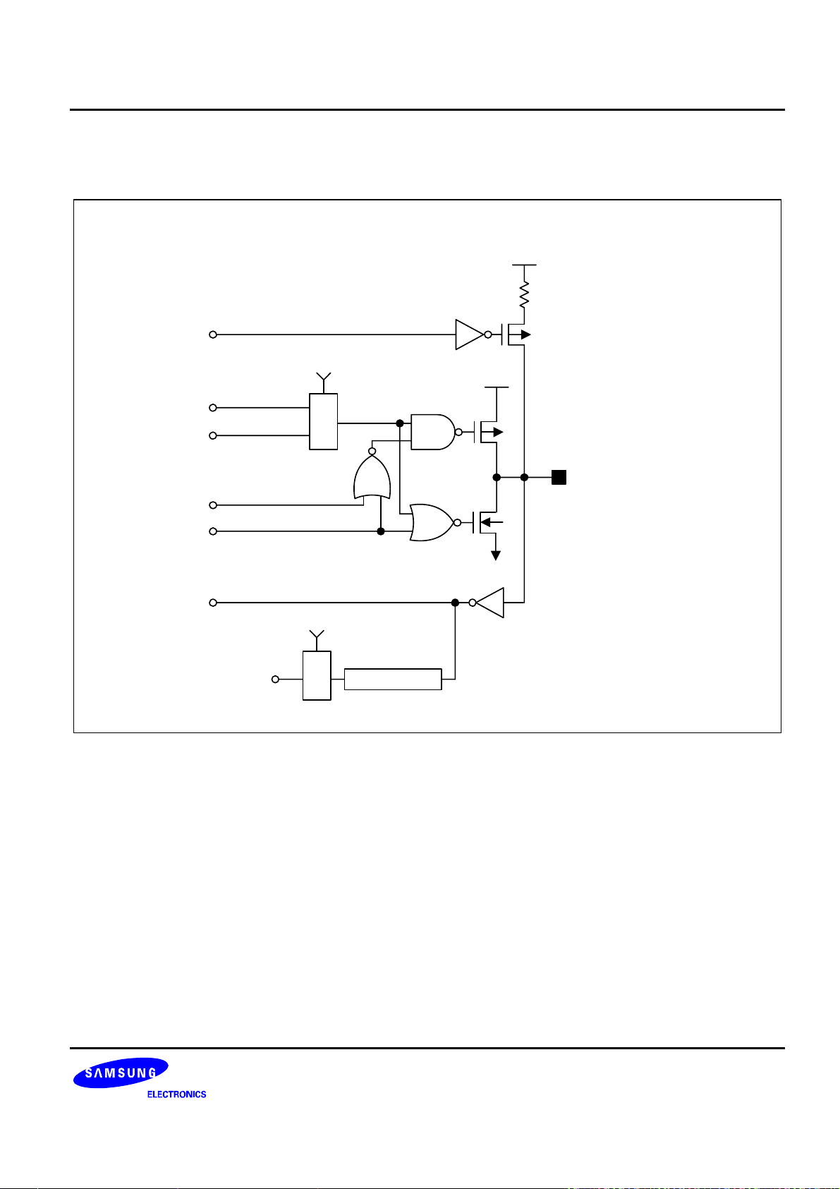
PIN CIRCUITS
V
DD
Pull-Up
Resistor
(67k
Ω
Pull-up
Enable
Data
Output Disable
V
DD
- typ)
INPUT/OUTPUT
External
Interrupt
Stop
V
SS
Noise
Filter
Figure 1-3. Pin Circuit Type 1 (Port 0)
Stop
Release
1-6
Page 23

S3F80P5_UM_ REV1.00 PRODUCT OVERVIEW
PIN CIRCUITS (Continued)
V
DD
Pull-up
Resistor
Ω
-Typ)
(67k
Pull-up
Enable
V
DD
Data
INPUT/OU TPUT
Open-Drain
Output Disable
V
SS
Normal
Input
Noise
Filter
Figure 1-4. Pin Circuit Type 2 (Port 1)
1-7
Page 24

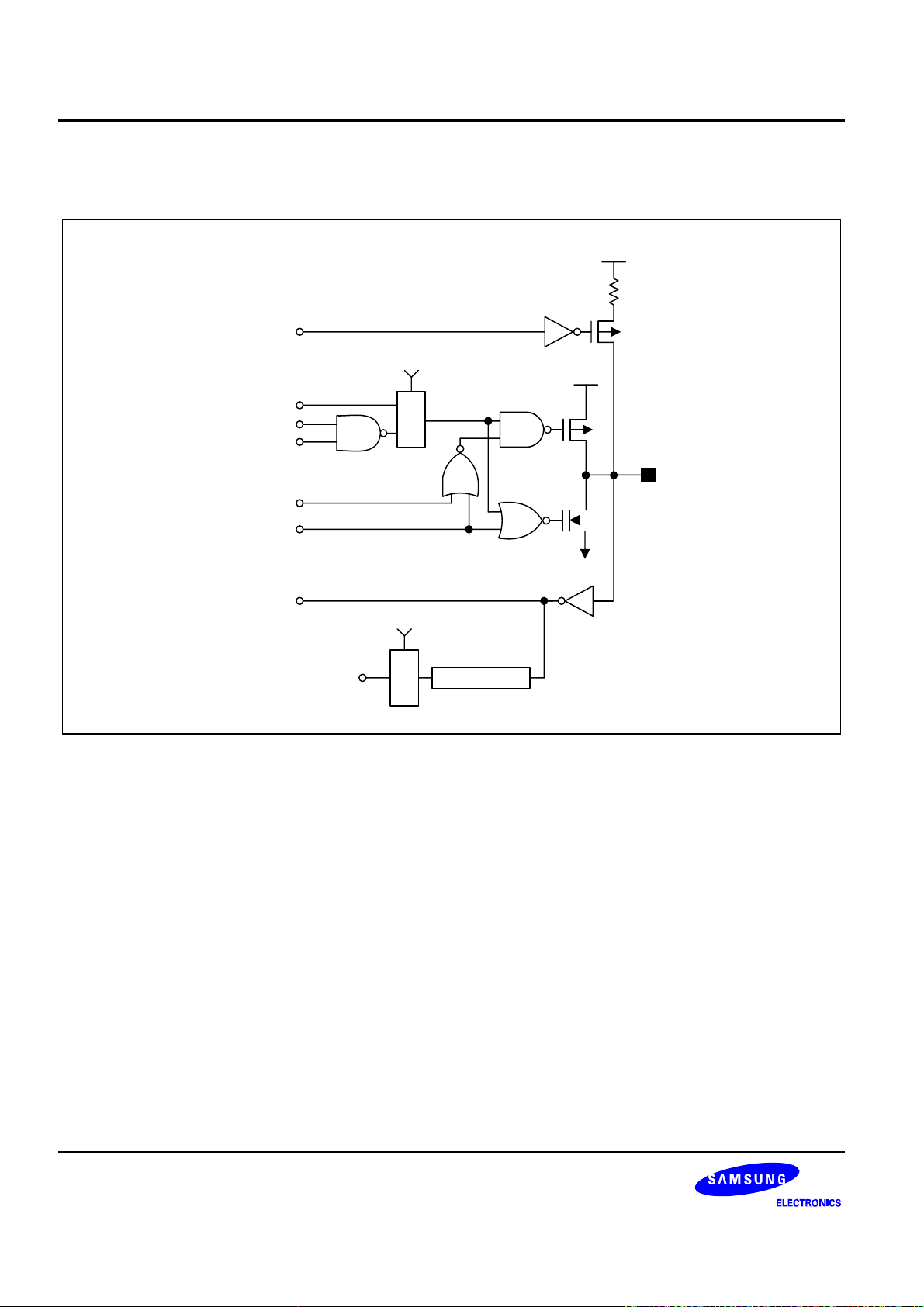
PRODUCT OVERVIEW S3F80P5_UM_ REV1.00
PIN CIRCUITS (Continued)
VDD
Pull-Up
Resistor
Pull-up
Enable
VDD
Data
Open-Drain
Output Disable
(67kΩ- typ)
INPUT/
OUTPUT
External
Interrupt
VSS
Noise
Filter
Figure 1-5. Pin Circuit Type 2 (Port 2)
1-8
Page 25
S3F80P5_UM_ REV1.00 PRODUCT OVERVIEW
PIN CIRCUITS (Continued)
VDD
Pull-up
Resistor
Pull-up
Enable
P3CON.2
VDD
(67kΩ-Typ)
Output Disable
Port 3.0 Data
T0_PWM
Open-Drain
P3.0 Input
T0CAP/T1CAP/T2CAP
M
U
X
P3CON.2,6,7
M
U
X
Data
Noise filter
Figure 1-6. Pin Circuit Type 4 (P3.0)
P3.0/T0PWM/T0CAP/
T1CAP/T2C AP
VSS
1-9
Page 26
PRODUCT OVERVIEW S3F80P5_UM_ REV1.00
PIN CIRCUITS (Continued)
VDD
Pull-up
Resistor
Pull-up
Enable
P3CON.5
VDD
(67kΩ-Typ)
Port 3.1 Data
Carrier On/Off (P3DAT.7)
CACON.2
Open-Drain
Output
Disable
P3.1 Input
T0CK
M
U
X
P3CON.5,6,7
M
U
X
Data
P3.1/REM/T0CK
VSS
Noise filter
Figure 1-7. Pin Circuit Type 5 (P3.1)
1-10
Page 27

S3F80P5_UM_ REV1.00 ADDRESS SPACE
2 ADDRESS SPACE
OVERVIEW
The S3F80P5 microcontroller has two types of address space:
— Internal program memory (Flash memory)
— Internal register file
A 16-bit address bus supports program memory operations. A separate 8-bit register bus carries addresses and
data between the CPU and the register file.
The S3F80P5 has a programmable internal 18-Kbytes Flash ROM. An external memory interface is not
implemented.
There are 333 mapped registers in the internal register file. Of these, 272-byte are for general-purpose use. (This
number includes a 16-byte working register common area that is used as a “scratch area” for data operations, a
192-byte prime register area, and a 64-byte area (Set 2) that is also used for stack operations). Twenty-two 8-bit
registers are used for CPU and system control and 39 registers are mapped peripheral control and data registers.
2-1
Page 28
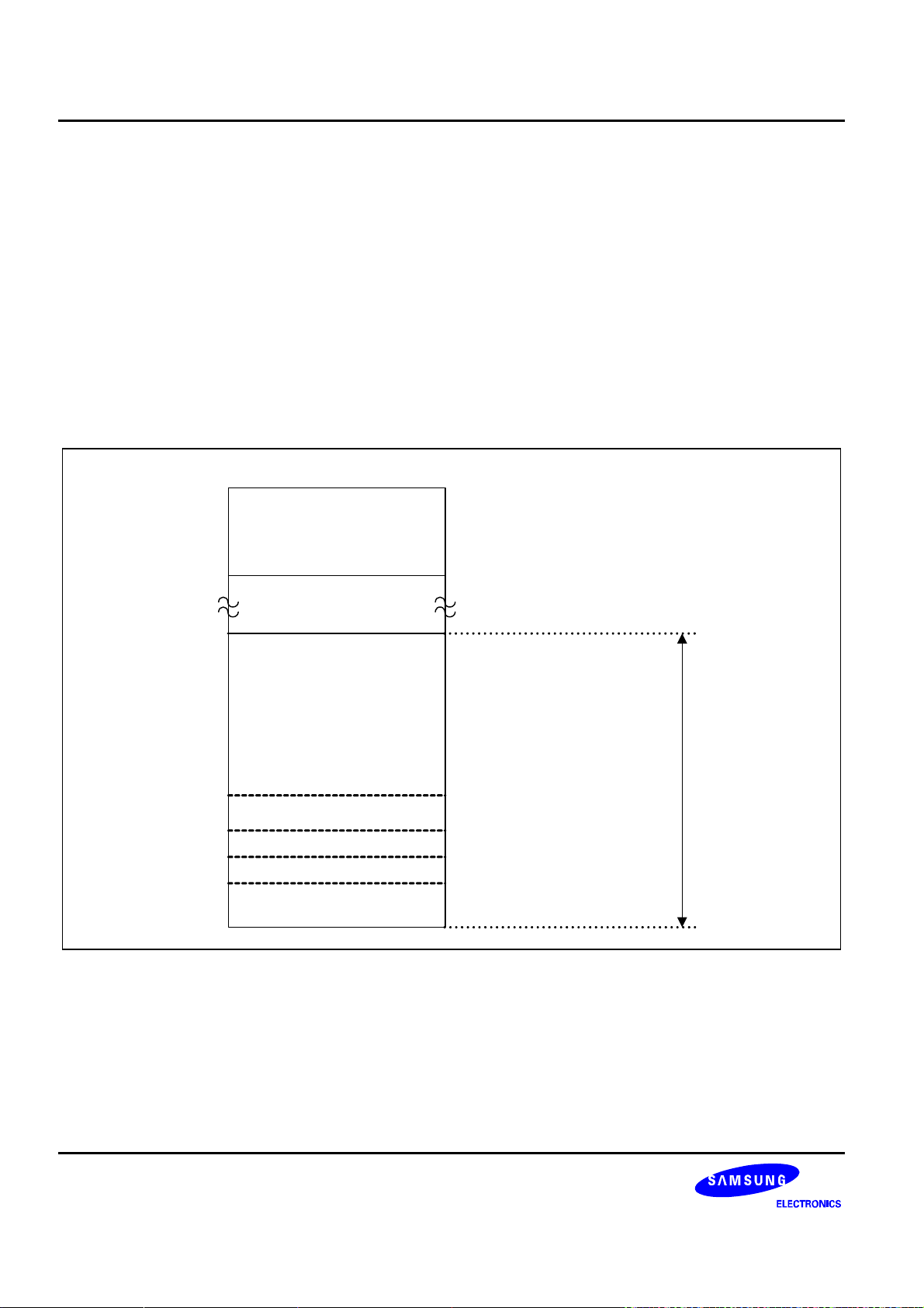
ADDRESS SPACE S3F80P5_UM_ REV1.00
PROGRAM MEMORY
Program memory stores program code or table data. The S3F80P5 has 18-Kbyte of internal programmable Flash
memory. The program memory address range is therefore 0000H–47FFH of Flash memory (See Figure 2-1).
The first 256 bytes of the program memory (0H–0FFH) are reserved for interrupt vector addresses. Unused
locations (0000H – 00FFH except 03CH, 03DH, 03EH and 03FH) in this address range can be used as normal
program memory. The location 03CH, 03DH, 03EH and 03FH is used as smart option ROM cell. If you use the
vector address area to store program code, be careful to avoid overwriting vector addresses stored in these
locations.
The program memory address at which program execution starts after reset is 0100H(default). If you use ISP
sectors as the ISP
TM
software storage, the reset vector address can be changed by setting the Smart Option.
(Refer to Figure 2-2).
(Decimal) (HEX)
65,536
1Kbyte
Internal RAM
FFFFH
TM
FC00H
16,383
Internal
Program
Memory
(Flash)
Note 1
ISP Sector
255
Interrupt Vector Area
Smart Option Rom Cell
000H
47FFH
S3F80P5(18Kbyte)
01FFH, 02FFH, 04FFH or 08FFH
0FFH
03FH
03CH
Figure 2-1. Program Memory Address Space
NOTES:
1. The size of ISP
related to the ISP, ISP reset vector address can be changed one of addresses to be select (200H, 300H, 500H or
900H).
2. ISP
TM
sector can store On Board Program Software (Refer to chapter 13. Embedded Flash Memory Interface).
TM
sector can be varied by Smart Option. (Refer to Figure 2-2). According to the smart option setting
2-2
Page 29
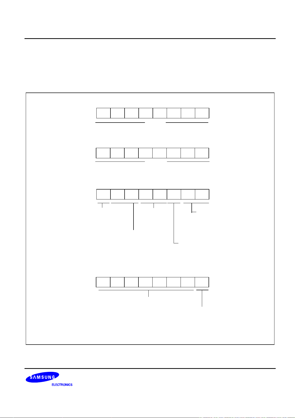
S3F80P5_UM_ REV1.00 ADDRESS SPACE
SMART OPTION
Smart option is the program memory option for starting condition of the chip. The program memory addresses
used by smart option are from 003CH to 003FH. The S3F80P5 only use 003EH and 003FH. User can write any
value in the not used addresses (003CH and 003DH). The default value of smart option bits in program memory
is 0FFH (Normal reset vector address 100H, ISP protection disable). Before execution the program memory
code, user can set the smart option bits according to the hardware option for user to want to select.
ROM Address: 003CH
.7 .6 .5 .4 .3 .2 .1 .0MSB LSB
Not used
ROM Address: 003DH
.7 .6 .5 .4 .3 .2 .1 .0MSB LSB
Not used
.7 .6 .5 .4 .3 .2 .1 .0MSB LSB
ISP Reset Vector Change Selection Bit:
0 = OBP Reset vector address
1 = Normal vector (address 100H)
ISP Reset Vector Address Selection Bits:
00 = 200H (ISP Area size: 256 bytes)
01 = 300H (ISP Area size: 512 bytes)
10 = 500H (ISP Area size: 1024 bytes)
11 = 900H (ISP Area size: 2048 bytes)
.7 .6 .5 .4 .3 .2 .1 .0MSB LSB
ROM Address: 003EH
(1)
Not used
ISP Protection Size
Selection Bits:
(4)
00 = 256 bytes
01 = 512 bytes
(2)
10 = 1024 bytes
11 = 2048 bytes
ISP Protection Enable/Disable Bit:
(3)
0 = Enable (Not erasable)
1 = Disable (Erasable)
ROM Address: 003FH
Not used
RESET Control Bit
(5)
0 = External interrupts by P0 and P2 or
SED&R generate the reset signal
1 = External interrupts by P0 and P2 or
SED&R do not generate the reset signal
Figure 2-2. Smart Option
2-3
Page 30

ADDRESS SPACE S3F80P5_UM_ REV1.00
NOTES
1. By setting ISP Reset Vector Change Selection Bit (3EH.7) to ‘0’, user can have the available ISP
area.
If ISP Reset Vector Change Selection Bit (3EH.7) is ‘1’, 3EH.6 and 3EH.5 are meaningless.
2. If ISP Reset Vector Change Selection Bit (3EH.7) is ‘0’, user must change ISP reset vector address
from 0100H to some address which user want to set reset address (0200H, 0300H, 0500H or
0900H).
If the reset vector address is 0200H, the ISP area can be assigned from 0100H to 01FFH (256bytes).
If 0300H, the ISP area can be assigned from 0100H to 02FFH (512bytes). If 0500H, the ISP area can
be assigned from 0100H to 04FFH (1024bytes). If 0900H, the ISP area can be assigned from 0100H
to 08FFH (2048bytes).
3. If ISP Protection Enable/Disable Bit is ‘0’, user can’t erase or program the ISP area selected by
3EH.1 and 3EH.0 in flash memory.
4. User can select suitable ISP protection size by 3EH.1 and 3EH.0. If ISP Protection Enable/Disable Bit
(3EH.2) is ‘1’, 3EH.1 and 3EH.0 are meaningless.
5. External interrupts can be used to release stop mode. When RESET Control Bit (3FH.0) is ‘0’ and
external interrupts is enabled, external interrupts wake MCU from stop mode and generate reset
signal. Any falling edge input signals of P0 can wake MCU from stop mode and
generate reset signal.
When RESET Control Bit (3FH.0) is ‘1’, S3F80P5 is only released stop mode and is not generated
reset signal.
2-4
Page 31

S3F80P5_UM_ REV1.00 ADDRESS SPACE
REGISTER ARCHITECTURE
In the S3F80P5 implementation, the upper 64-byte area of register files is expanded two 64-byte areas, called set
1 and set 2. The upper 32-byte area of set 1 is further expanded two 32-byte register banks (bank 0 and bank 1),
and the lower 32-byte area is a single 32-byte common area.
In case of S3F80P5 the total number of addressable 8-bit registers is 333. Of these 333 registers, 22 bytes are for
CPU and system control registers, 39 bytes are for peripheral control and data registers, 16 bytes are used as
shared working registers, and 272 registers are for general-purpose use.
The extension of register space into separately addressable areas (sets, banks) is supported by various
addressing mode restrictions: the select bank instructions, SB0 and SB1.
Specific register types and the area occupied in the S3F80P5 internal register space are summarized in Table 2-
1.
Table 2-1. The Summary of S3F80P5 Register Type
Register Type Number of Bytes
General-purpose registers (including the 16-byte common working register
area, the 64-byte set 2 area and 192-byte prime register area of page 0)
CPU and system control registers 22
Mapped clock, peripheral, and I/O control and data registers (bank 0: 27
registers, bank 1: 12 registers)
Total Addressable Bytes 333
272
39
2-5
Page 32

ADDRESS SPACE S3F80P5_UM_ REV1.00
64
Bytes
FFH
E0H
DFH
D0H
CFH
C0H
Set 1
Bank1
Bank 0
System and
Peripheral
Control Register
(Register Addressing
Mode)
System Register
(Register Addressing
Mode)
Working Register
(Working Register
Addressing only)
E0H
32
Bytes
32
Bytes
Set 2
Page 0
General Purpose
Data Register
(Indirect Register or
Indexed Addressing
Modes or
Stack Operations)
Page 0
FFH
256
Bytes
C0H
BFH
Prime
192
Bytes
Data Register
(All Addressing
Mode)
Figure 2-3. Internal Register File Organization
00H
2-6
Page 33

S3F80P5_UM_ REV1.00 ADDRESS SPACE
REGISTER PAGE POINTER (PP)
The S3C8/S3F8-series architecture supports the logical expansion of the physical 333-byte internal register files
(using an 8-bit data bus) into as many as 16 separately addressable register pages. Page addressing is
controlled by the register page pointer PP (DFH, Set 1, and Bank0). In the S3F80P5 microcontroller, a paged
register file expansion is not implemented and the register page pointer settings therefore always point to “page
0”.
Following a reset, the page pointer's source value (lower nibble) and destination value (upper nibble) are always
'0000'automatically. Therefore, S3F80P5 is always selected page 0 as the source and destination page for
register addressing. These page pointer (PP) register settings, as shown in Figure 2-4, should not be modified
during normal operation.
Register Page Pointer (PP)
DFH ,Set 1, Bank0, R/W
MSB LSB
Destination Register Page Seleciton Bits:
NOTE:
.7 .6 .5 .4 .3 .2 .1 .0
Source Register Page Selection Bits:
Destination: page 0
A hardware reset operation writes the 4-bit destination and source values shown
above to the register page pointer. These values should not be modified to
address other pages.
0 0 0 00 0 0 0
Source: page 0
Figure 2-4. Register Page Pointer (PP)
2-7
Page 34

ADDRESS SPACE S3F80P5_UM_ REV1.00
REGISTER SET 1
The term set 1 refers to the upper 64 bytes of the register file, locations C0H–FFH.
The upper 32-byte area of this 64-byte space (E0H–FFH) is divided into two 32-byte register banks, bank 0 and
bank 1. The set register bank instructions SB0 or SB1 are used to address one bank or the other. In the S3F80P5
microcontroller, bank 1 is implemented. The set register bank instructions, SB0 or SB1, are used to address one
bank or the other. A hardware reset operation always selects bank 0 addressing.
The upper two 32-byte area of set 1, bank 0, (E0H–FFH) contains 31mapped system and peripheral control
registers. Also, the upper 32-byte area of set1, bank1 (E0H–FFH) contains 16 mapped peripheral control register.
The lower 32-byte area contains 15 system registers (D0H–DFH) and a 16-byte common working register area
(C0H–CFH). You can use the common working register area as a “scratch” area for data operations being
performed in other areas of the register file.
Registers in set 1 locations are directly accessible at all times using the Register addressing mode. The 16-byte
working register area can only be accessed using working register addressing. (For more information about
working register addressing, please refer to Chapter 3, “Addressing Modes,”)
REGISTER SET 2
The same 64-byte physical space that is used for set 1 locations C0H–FFH is logically duplicated to add another
64 bytes of register space. This expanded area of the register file is called set 2. The set 2 locations (C0H–FFH)
is accessible on page 0 in the S3F80P5 register space.
The logical division of set 1 and set 2 is maintained by means of addressing mode restrictions: You can use only
Register addressing mode to access set 1 locations; to access registers in set 2, you must use Register Indirect
addressing mode or Indexed addressing mode.
The set 2 register area is commonly used for stack operations.
2-8
Page 35

S3F80P5_UM_ REV1.00 ADDRESS SPACE
PRIME REGISTER SPACE
The lower 192 bytes of the 256-byte physical internal register file (00H–BFH) are called the prime register space
or, more simply, the prime area. You can access registers in this address using any addressing mode. (In other
words, there is no addressing mode restriction for these registers, as is the case for set 1 and set 2 registers.).
The prime register area on page 0 is immediately addressable following a reset.
Set 1
FFH
Bank 0
FCH
Bank 1
FFH
Page 0
E0H
D0H
C0H
CPU and system control
General-purpose
Peripheral and IO
C0H
BFH
00H
Set 2
Page 0
Prime
Register
Area
Figure 2-5. Set 1, Set 2, and Prime Area Register Map
2-9
Page 36

ADDRESS SPACE S3F80P5_UM_ REV1.00
WORKING REGISTERS
Instructions can access specific 8-bit registers or 16-bit register pairs using either 4-bit or 8-bit address fields.
When 4-bit working register addressing is used, the 256-byte register file can be seen by the programmer as
consisting of 32 8-byte register groups or "slices." Each slice consists of eight 8-bit registers.
Using the two 8-bit register pointers, RP1 and RP0, two working register slices can be selected at any one time to
form a 16-byte working register block. Using the register pointers, you can move this 16-byte register block
anywhere in the addressable register file, except for the set 2 area.
The terms slice and block are used in this manual to help you visualize the size and relative locations of selected
working register spaces:
— One working register slice is 8 bytes (eight 8-bit working registers; R0–R7 or R8–R15)
— One working register block is 16 bytes (sixteen 8-bit working registers; R0–R15)
All of the registers in an 8-byte working register slice have the same binary value for their five most significant
address bits. This makes it possible for each register pointer to point to one of the 24 slices in the register file.
The base addresses for the two selected 8-byte register slices are contained in register pointers RP0 and RP1.
After a reset, RP0 and RP1 always point to the 16-byte common area in set 1 (C0H–CFH).
1 1 1 1 1 X X X
RP1 (Registers R8-R15)
Each register pointer points to
one 8-byte slice of the register
space, selecting a total 16-byte
working register block.
0 0 0 0 0 X X X
RP0 (Registers R0-R7)
Figure 2-6. 8-Byte Working Register Areas (Slices)
Slice 32
~
Slice 1
FFH
F8H
F7H
F0H
Set 1
Only
CFH
C0H
~
10H
0FH
08H
07H
00H
2-10
Page 37

S3F80P5_UM_ REV1.00 ADDRESS SPACE
USING THE REGISTER POINTERS
Register pointers RP0 and RP1, mapped to addresses D6H and D7H in set 1, are used to select two movable
8-byte working register slices in the register file. After a reset, they point to the working register common area:
RP0 points to addresses C0H–C7H, and RP1 points to addresses C8H–CFH.
To change a register pointer value, you load a new value to RP0 and/or RP1 using an SRP or LD instruction (see
Figures 2-6 and 2-7).
With working register addressing, you can only access those two 8-bit slices of the register file that are currently
pointed to by RP0 and RP1. You cannot, however, use the register pointers to select a working register space in
set 2, C0H–FFH, because these locations can be accessed only using the Indirect Register or Indexed
addressing modes.
The selected 16-byte working register block usually consists of two contiguous 8-byte slices. As a general
programming guideline, we recommend that RP0 point to the "lower" slice and RP1 point to the "upper" slice (see
Figure 2-6). In some cases, it may be necessary to define working register areas in different (non-contiguous)
areas of the register file. In Figure 2-7, RP0 points to the "upper" slice and RP1 to the "lower" slice.
Because a register pointer can point to the either of the two 8-byte slices in the working register block, you can
define the working register area very flexibly to support program requirements.
PROGRAMMING TIP — Setting the Register Pointers
SRP #70H ; RP0 ← 70H, RP1 ← 78H
SRP1 #48H ; RP0 ← no change, RP1 ← 48H,
SRP0 #0A0H ; RP0 ← A0H, RP1 ← no change
CLR RP0 ; RP0 ← 00H, RP1 ← no change
LD RP1,#0F8H ; RP0 ← no change, RP1 ← 0F8H
Register File
Contains 32
8-Byte Slices
0 0 0 0 1 X X X
RP1
0 0 0 0 0 X X X
RP0
Figure 2-7. Contiguous 16-Byte Working Register Block
8-Byte Slice
8-Byte Slice
0FH (R15)
08H
07H
00H (R0)
16-byte
contiguous
working
register block
2-11
Page 38

ADDRESS SPACE S3F80P5_UM_ REV1.00
F7H (R7)
8-Byte Slice
F0H (R0)
Register File
1 1 1 1 0 X X X
RP0
0 0 0 0 0 X X X
RP1
Contains 32
8-Byte Slices
07H (R15)
8-Byte Slice
00H (R0)
16-byte non-contiguous
working register block
Figure 2-8. Non-Contiguous 16-Byte Working Register Block
PROGRAMMING TIP — Using the RPs to Calculate the Sum of a Series of Registers
Calculate the sum of registers 80H–85H using the register pointer. The register addresses 80H through 85H
contains the values 10H, 11H, 12H, 13H, 14H, and 15 H, respectively:
SRP0 #80H ; RP0 ← 80H
ADD R0,R1 ; R0 ← R0 + R1
ADC R0,R2 ; R0 ← R0 + R2 + C
ADC R0,R3 ; R0 ← R0 + R3 + C
ADC R0,R4 ; R0 ← R0 + R4 + C
ADC R0,R5 ; R0 ← R0 + R5 + C
The sum of these six registers, 6FH, is located in the register R0 (80H). The instruction string used in this
example takes 12 bytes of instruction code and its execution time is 36 cycles. If the register pointer is not used to
calculate the sum of these registers, the following instruction sequence would have to be used:
ADD 80H,81H ; 80H ← (80H) + (81H)
ADC 80H,82H ; 80H ← (80H) + (82H) + C
ADC 80H,83H ; 80H ← (80H) + (83H) + C
ADC 80H,84H ; 80H ← (80H) + (84H) + C
ADC 80H,85H ; 80H ← (80H) + (85H) + C
Now, the sum of the six registers is also located in register 80H. However, this instruction string takes 15 bytes of
instruction code instead of 12 bytes, and its execution time is 50 cycles instead of 36 cycles.
2-12
Page 39

S3F80P5_UM_ REV1.00 ADDRESS SPACE
REGISTER ADDRESSING
The S3C8-series register architecture provides an efficient method of working register addressing that takes full
advantage of shorter instruction formats to reduce execution time.
With Register (R) addressing mode, in which the operand value is the content of a specific register or register
pair, you can access all locations in the register file except for set 2. With working register addressing, you use a
register pointer to specify an 8-byte working register space in the register file and an 8-bit register within that
space.
Registers are addressed either as a single 8-bit register or as a paired 16-bit register space. In a 16-bit register
pair, the address of the first 8-bit register is always an even number and the address of the next register is always
an odd number. The most significant byte of the 16-bit data is always stored in the even-numbered register; the
least significant byte is always stored in the next (+ 1) odd-numbered register.
Working register addressing differs from Register addressing because it uses a register pointer to identify a
specific 8-byte working register space in the internal register file and a specific 8-bit register within that space.
MSB
Rn
LSB
Rn+1
n = Even address
Figure 2-9. 16-Bit Register Pair
2-13
Page 40

ADDRESS SPACE S3F80P5_UM_ REV1.00
Special-Purpose Registers General-Purpose Registers
Bank 1
FFH
E0H
D0H
C0H
BFH
RP1
RP0
Each register pointer (RP) can independently point to one
of the 24 8-byte "slices" of the register file (other than set
2). A fte r a re s e t, RP0 p o in ts to lo c a tio n s C0H -C7H a n d
RP 1 to lo c a tio n s C8H - C F H (tha t is , to th e c o mm o n
working register area).
NOTE: In the S3F80K 5 m icrocontroller,only page0 is
Bank 0
Control
Registers
System
Registers
Register
Pointers
implemented.Page0 containsall of the
addressable registers in the internal register file.
FFH
Set 2
CFH
C0H
Prime
Registers
00H
Register Addressing Only
Can be Pointed by Register Pointer
Figure 2-10. Register File Addressing
Page 0
All
Addressing
Modes
Page 0
Indirect
Register,
Indexed
Addressing
Modes
2-14
Page 41

S3F80P5_UM_ REV1.00 ADDRESS SPACE
COMMON WORKING REGISTER AREA (C0H–CFH)
After a reset, register pointers RP0 and RP1 automatically select two 8-byte register slices in set 1, locations
C0H–CFH, as the active 16-byte working register block:
RP0 → C0H–C7H
RP1 → C8H–CFH
This 16-byte address range is called common area. That is, locations in this area can be used as working
registers by operations that address any location on any page in the register file. Typically, these working
registers serve as temporary buffers for data operations.
FFH
F0H
E0H
D0H
C0H
Following a hareware reset, register
pointers RP0 and RP1 point to the
common working register
area, locations C0H-CFH.
RP0 =
RP1 =
1100 000
Set 1
FFH
C0H
BFH
0
01100 100
00H
Figure 2-11. Common Working Register Area
Page 0
Set 2
Page 0
Prime
Area
~~
2-15
Page 42

ADDRESS SPACE S3F80P5_UM_ REV1.00
PROGRAMMING TIP — Addressing the Common Working Register Area
As the following examples show, you should access working registers in the common area, locations C0H–CFH,
using working register addressing mode only.
Example 1:
LD 0C2H,40H ; Invalid addressing mode!
Use working register addressing instead:
SRP #0C0H
LD R2,40H ; R2 (C2H) ← the value in location 40H
Example 2:
ADD 0C3H,#45H ; Invalid addressing mode!
Use working register addressing instead:
SRP #0C0H
ADD R3,#45H ; R3 (C3H) ← R3 + 45H
4-Bit Working Register Addressing
Each register pointer defines a movable 8-byte slice of working register space. The address information stored in
a register pointer serves as an addressing "window" that makes it possible for instructions to access working
registers very efficiently using short 4-bit addresses. When an instruction addresses a location in the selected
working register area, the address bits are concatenated in the following way to form a complete 8-bit address:
— The high-order bit of the 4-bit address selects one of the register pointers ("0" selects RP0; "1" selects RP1);
— The five high-order bits in the register pointer select an 8-byte slice of the register space;
— The three low-order bits of the 4-bit address select one of the eight registers in the slice.
As shown in Figure 2-11, the result of this operation is that the five high-order bits from the register pointer are
concatenated with the three low-order bits from the instruction address to form the complete address. As long as
the address stored in the register pointer remains unchanged, the three bits from the address will always point to
an address in the same 8-byte register slice.
Figure 2-12 shows a typical example of 4-bit working register addressing. The high-order bit of the instruction
'INC R6' is "0", which selects RP0. The five high-order bits stored in RP0 (01110B) are concatenated with the
three low-order bits of the instruction's 4-bit address (110B) to produce the register address 76H (01110110B).
2-16
Page 43

S3F80P5_UM_ REV1.00 ADDRESS SPACE
RP0
RP1
Selects
RP0 or RP1
Register pointer
provides five
high-order bits
Figure 2-12. 4-Bit Working Register Addressing
RP0
0 1 1 1 0 0 0 0
Address
Together they create an
8-bit register address
OPCODE
0 1 1 1 0 0 01
4-bit address
procides three
low-order bits
RP1
0 1 1 1 0 1 1 0
Figure 2-13. 4-Bit Working Register Addressing Example
2-17
Selects RP0
Register
address
(76H)
R6
0110 1110
OPCODE
Instruction:
'INC R6'
Page 44

ADDRESS SPACE S3F80P5_UM_ REV1.00
8-BIT WORKING REGISTER ADDRESSING
You can also use 8-bit working register addressing to access registers in a selected working register area. To
initiate 8-bit working register addressing, the upper four bits of the instruction address must contain the value
1100B. This 4-bit value (1100B) indicates that the remaining four bits have the same effect as 4-bit working
register addressing.
As shown in Figure 2-13, the lower nibble of the 8-bit address is concatenated in much the same way as for 4-bit
addressing: Bit 3 selects either RP0 or RP1, which then supplies the five high-order bits of the final address. The
three low-order bits of the complete address are provided by the original instruction.
Figure 2-14 shows an example of 8-bit working register addressing. The four high-order bits of the instruction
address (1100B) specify 8-bit working register addressing. Bit 4 ("1") selects RP1 and the five high-order bits in
RP1 (10101B) become the five high-order bits of the register address. The three low-order bits of the register
address (011) are provided by the three low-order bits of the 8-bit instruction address. The five-address bits from
RP1 and the three address bits from the instruction are concatenated to form the complete register address,
0ABH (10101011B).
These address
bits indicate
8-bit working
register
addressing
RP0
RP1
Selects
RP0 or RP1
Address
1 1 0 0
Register pointer
provides five
high-order bits
8-bit physical address
8-bit logical
address
Three loworder bits
Figure 2-14. 8-Bit Working Register Addressing
2-18
Page 45

S3F80P5_UM_ REV1.00 ADDRESS SPACE
01 1 10 1 10
Specifies working
register addressing
Figure 2-15. 8-Bit Working Register Addressing Example
RP0
01 1 1 0 0 000 1 1 1 0 0 0 0
Selects RP1
R11
8-bit address
from instruction
'LD R11, R2'
Register address (0ABH) 01101 110
RP1
2-19
Page 46

ADDRESS SPACE S3F80P5_UM_ REV1.00
SYSTEM AND USER STACKS
S3C8-series microcontrollers use the system stack for subroutine calls and returns and to store data. The PUSH
and POP instructions are used to control system stack operations. The S3F80P5 architecture supports stack
operations in the internal register file.
Stack Operations
Return addresses for procedure calls, interrupts and data are stored on the stack. The contents of the PC are
saved to stack by a CALL instruction and restored by the RET instruction. When an interrupt occurs, the contents
of the PC and the FLAGS registers are pushed to the stack. The IRET instruction then pops these values back to
their original locations. The stack address value is always decreased by one before a push operation and
increased by one after a pop operation. The stack pointer (SP) always points to the stack frame stored on the top
of the stack, as shown in Figure 2-15.
High Address
PCL
Top of
stack
PCL
PCH
Stack contents
after a call
instruction
Top of
stack
Low Address
PCH
Flags
Stack contents
after an
interrupt
Figure 2-16. Stack Operations
User-Defined Stacks
You can freely define stacks in the internal register file as data storage locations. The instructions PUSHUI,
PUSHUD, POPUI, and POPUD support user-defined stack operations.
Stack Pointers (SPL)
Register location D9H contains the 8-bit stack pointer (SPL) that is used for system stack operations. After a
reset, the SPL value is undetermined. Because only internal memory 256-byte is implemented in The S3F80P5,
the SPL must be initialized to an 8-bit value in the range 00–FFH.
2-20
Page 47

S3F80P5_UM_ REV1.00 ADDRESS SPACE
PROGRAMMING TIP — Standard Stack Operations Using PUSH and POP
The following example shows you how to perform stack operations in the internal register file using PUSH and
POP instructions:
LD SPL,#0FFH ; SPL ← FFH
; (Normally, the SPL is set to 0FFH by the initialization
; routine)
•
•
PUSH PP ; Stack address 0FEH ← PP
PUSH RP0 ; Stack address 0FDH ← RP0
PUSH RP1 ; Stack address 0FCH ← RP1
PUSH R3 ; Stack address 0FBH ← R3
•
•
POP R3 ; R3 ← Stack address 0FBH
POP RP1 ; RP1 ← Stack address 0FCH
POP RP0 ; RP0 ← Stack address 0FDH
POP PP ; PP ← Stack address 0FEH
•
•
2-21
Page 48

ADDRESS SPACE S3F80P5_UM_ REV1.00
NOTES
2-22
Page 49

S3F80P5_UM_ REV1.00 ADDRESSING MODES
3 ADDRESSING MODES
OVERVIEW
The program counter is used to fetch instructions that are stored in program memory for execution. Instructions
indicate the operation to be performed and the data to be operated on. Addressing mode is the method used to
determine the location of the data operand. The operands specified in instructions may be condition codes,
immediate data, or a location in the register file, program memory, or data memory.
The S3C8/S3F8-series instruction set supports seven explicit addressing modes. Not all of these addressing
modes are available for each instruction:
— Register (R)
— Indirect Register (IR)
— Indexed (X)
— Direct Address (DA)
— Indirect Address (IA)
— Relative Address (RA)
— Immediate (IM)
3-1
Page 50

ADDRESSING MODES S3F80P5_UM_ REV1.00
REGISTER ADDRESSING MODE (R)
In Register addressing mode, the operand is the content of a specified register or register pair (see Figure 3-1).
Working register addressing differs from Register addressing because it uses a register pointer to specify an 8byte working register space in the register file and an 8-bit register within that space (see Figure 3-2).
Program Memory Register File
8-bit register
file address
One-Operand
Instruction
(Example)
Sample Instruction:
DEC CNTR ; Where CNTR is the label of an 8-bit register address
dst
OPCODE
Points to one
OPERAND
register in register
file
Value used in
instruction execution
4-bit
Working Register
Two-Operand
Instruction
(Example)
Figure 3-1. Register Addressing
Register File
MSB Points to
RP0 ot RP1
Program Memory
dst
OPCODE
Sample Instruction:
ADD R1, R2 ; Where R1 and R2 are registers in the curruntly
src
3 LSBs
Points to the
woking register
(1 of 8)
selected working register area.
RP0 or RP1
Selected RP
points
to start
of working
register
block
OPERAND
Figure 3-2. Working Register Addressing
3-2
Page 51

S3F80P5_UM_ REV1.00 ADDRESSING MODES
INDIRECT REGISTER ADDRESSING MODE (IR)
In Indirect Register (IR) addressing mode, the content of the specified register or register pair is the address of
the operand. Depending on the instruction used, the actual address may point to a register in the register file, to
program memory (ROM), or to an external memory space, if implemented (see Figures 3-3 through 3-6).
You can use any 8-bit register to indirectly address another register. Any 16-bit register pair can be used to
indirectly address another memory location. Remember, however, that locations C0H–FFH in set 1 cannot be
accessed using Indirect Register addressing mode.
Program Memory Register File
8-bit register
file address
One-Operand
Instruction
(Example)
dst
OPCODE
Points to one
ADDRESS
register in register
file
Address of operand
used by instruction
Value used in
instruction execution
Sample Instruction:
RL @SHIFT ; Where SHIFT is the label of an 8-bit register address.
OPERAND
Figure 3-3. Indirect Register Addressing to Register File
3-3
Page 52

ADDRESSING MODES S3F80P5_UM_ REV1.00
INDIRECT REGISTER ADDRESSING MODE (Continued)
Register File
Program Memory
Example
Instruction
References
Program
Memory
Sample Instructions:
CALL @RR2
JP @RR2
Register
dst
OPCODE
Points to
Register Pair
Value used in
instruction
Pair
Program Memory
OPERAND
Figure 3-4. Indirect Register Addressing to Program Memory
16-Bit
Address
Points to
Program
Memory
3-4
Page 53

S3F80P5_UM_ REV1.00 ADDRESSING MODES
INDIRECT REGISTER ADDRESSING MODE (Continued)
Register File
MSB Points to
4-bit
Working
Register
Address
Program Memory
dst
OPCODE
src
RP0 or RP1
3 LSBs
Point to the
Woking Register
(1 of 8)
RP0 or RP1
~ ~
ADDRESS
Selected
RP points
to start of
woking register
block
~ ~
Sample Instruction:
OR R3, @R6
Value used in
instruction
OPERAND
Figure 3-5. Indirect Working Register Addressing to Register File
3-5
Page 54

ADDRESSING MODES S3F80P5_UM_ REV1.00
INDIRECT REGISTER ADDRESSING MODE (Continued)
Register File
MSB Points to
4-bit Working
Register Address
Example Instruction
References either
Program Memory or
Data Memory
Program Memory
dst
OPCODE
src
RP0 or RP1
Next 2-bit Point
to Working
Register Pair
(1 of 4)
LSB Selects
Value used in
Instruction
RP0 or RP1
Register
Pair
Program Memory
or
Data Memory
OPERAND
Selected
RP points
to start of
working
register
block
16-Bit
address
points to
program
memory
or data
memory
Sample Instructions:
LCD R5,@RR6 ; Program memory access
LDE R3,@RR14 ; External data memory access
LDE @RR4, R8 ; External data memory access
NOTE: LDE command is not available, because an external interface is not implemented
for the S3F80K5.
Figure 3-6. Indirect Working Register Addressing to Program or Data Memory
3-6
Page 55

S3F80P5_UM_ REV1.00 ADDRESSING MODES
INDEXED ADDRESSING MODE (X)
Indexed (X) addressing mode adds an offset value to a base address during instruction execution in order to
calculate the effective operand address (see Figure 3–7). You can use Indexed addressing mode to access
locations in the internal register file or in external memory (if implemented). You cannot, however, access
locations C0H–FFH in set 1 using indexed addressing.
In short offset Indexed addressing mode, the 8-bit displacement is treated as a signed integer in the range –128
to +127. This applies to external memory accesses only (see Figure 3–8).
For register file addressing, an 8-bit base address provided by the instruction is added to an 8-bit offset contained
in a working register. For external memory accesses, the base address is stored in the working register pair
designated in the instruction. The 8-bit or 16-bit offset given in the instruction is then added to the base address
(see Figure 3–9).
The only instruction that supports indexed addressing mode for the internal register file is the Load instruction
(LD). The LDC and LDE instructions support indexed addressing mode for internal program memory and for
external data memory (if implemented).
Register File
Two-Operand
Instruction
Example
Sample Instruction:
LD R0, #BASE[R1] ; Where BASE is an 8-bit immediate value.
Program Memory
Base Address
dst/src
OPCODE
x
MSB Points to
RP0 or RP1
Value used in
Instruction
+
3 LSBs
Points to one of the
Woking Registers
(1 of 8)
RP0 or RP1
~
OPERAND
~ ~
INDEX
~
Selected RP
points to
start of
working
register
block
Figure 3-7. Indexed Addressing to Register File
3-7
Page 56

ADDRESSING MODES S3F80P5_UM_ REV1.00
INDEXED ADDRESSING MODE (Continued)
Register File
MSB Points to
4-bit Working
Register Address
Program Memory
OFFSET
dst/src
OPCODE
x
RP0 or RP1
NEXT 2 BITS
Point to Working
Register Pair
(1 of 4)
LSB Selects
RP0 or RP1
~ ~
Register
Pair
Program Memory
or
Data Memory
Selected
RP points
to start of
working
register
block
16-Bit
address
added to
offset
+
8-Bit
16-Bit
16-Bit
Sample Instructions:
LDC R4, #04H[RR2] ; The values in the program address (RR2 + 04H)
are loaded into register R4.
LDE R4,#04H[RR2] ; Identical operation to L DC example, except that
external data memory is accessed.
NOTE:
LDE command is not available, because an external interface is not implemented
for the S3F80K5.
OPERAND
Value used in
Instruction
Figure 3-8. Indexed Addressing to Program or Data Memory with Short Offset
3-8
Page 57

S3F80P5_UM_ REV1.00 ADDRESSING MODES
INDEXED ADDRESSING MODE (Continued)
Register File
MSB Points to
4-bit Working
Register Address
Program Memory
OFFSET
OFFSET
dst/src
OPCODE
x
RP0 or RP1
NEXT 2 BITS
Point to Working
Register Pair
LSB Selects
RP0 or RP1
Register
Pair
Program Memory
or
Data Memory
~~
Selected
RP points
to start of
working
register
block
16-Bit
address
added to
offset
+
16-Bit
16-Bit
16-Bit
Sample Instructions:
LDC R4, #1000H[RR2] ; The values in the program address (RR2 + 1000H)
are loaded into register R4.
LDE R4,#1000H[RR2] ; Identical operation to LDC example, except that
external data memory is accessed.
NOTE:
LDE command is not available, because an external interface is not implemented
for the S3F80K5.
OPERAND
Value used in
Instruction
Figure 3-9. Indexed Addressing to Program or Data Memory
3-9
Page 58

ADDRESSING MODES S3F80P5_UM_ REV1.00
DIRECT ADDRESS MODE (DA)
In Direct Address (DA) mode, the instruction provides the operand's 16-bit memory address. Jump (JP) and Call
(CALL) instructions use this addressing mode to specify the 16-bit destination address that is loaded into the PC
whenever a JP or CALL instruction is executed.
The LDC and LDE instructions can use Direct Address mode to specify the source or destination address for
Load operations to program memory (LDC) or to external data memory (LDE), if implemented.
Program or
Data Memory
Memory
Program Memory
Address
Used
Upper Address Byte
Lower Address Byte
dst/src
Sample Instructions:
LDC R5,1234H ; The values in the program address (1234H)
LDE R5,1234H ; Identical operation to LDC example, except
NOTE: LDE command is not available, because an external interface is not
implemented for the S3F80K5.
"0" or "1"
OPCODE
are loaded into register R5.
that external data memory is accessed.
LSB Selects Program
Memory or Data Memory:
"0" = Program Memory
"1" = Data Memory
Figure 3-10. Direct Addressing for Load Instructions
3-10
Page 59

S3F80P5_UM_ REV1.00 ADDRESSING MODES
DIRECT ADDRESS MODE (Continued)
Program Memory
Next OPCODE
Program
Memory
Address
Used
Lower Address Byte
Upper Address Byte
OPCODE
Sample Instructions:
JP C,JOB1 ; Where JOB1 is a 16-bit immediate address
CALL DISPLAY ; Where DISPLAY is a 16-bit immediate address
Figure 3-11. Direct Addressing for Call and Jump Instructions
3-11
Page 60

ADDRESSING MODES S3F80P5_UM_ REV1.00
INDIRECT ADDRESS MODE (IA)
In Indirect Address (IA) mode, the instruction specifies an address located in the lowest 256 bytes of the program
memory. The selected pair of memory locations contains the actual address of the next instruction to be
executed. Only the CALL instruction can use the Indirect Address mode.
Because the Indirect Address mode assumes that the operand is located in the lowest 256 bytes of program
memory, only an 8-bit address is supplied in the instruction; the upper bytes of the destination address are
assumed to be all zeros.
Program Memory
Next Instruction
LSB Must be Zero
Current
Instruction
Lower Address Byte
Upper Address Byte
Sample Instruction:
CALL #40H ; The 16-bit value in program memory addresses 40H
and 41H is the subroutine start address.
dst
OPCODE
Program Memory
Locations 0-255
Figure 3-12. Indirect Addressing
3-12
Page 61

S3F80P5_UM_ REV1.00 ADDRESSING MODES
RELATIVE ADDRESS MODE (RA)
In Relative Address (RA) mode, a two's-complement signed displacement between – 128 and + 127 is specified
in the instruction. The displacement value is then added to the current PC value. The result is the address of the
next instruction to be executed. Before this addition occurs, the PC contains the address of the instruction
immediately following the current instruction.
Several program control instructions use the Relative Address mode to perform conditional jumps. The
instructions that support RA addressing are BTJRF, BTJRT, DJNZ, CPIJE, CPIJNE, and JR.
Program Memory
Next OPCODE
Displacement
Current Instruction
Sample Instructions:
JR ULT,$+OFFSET ; Where OFFSET is a value in the range +127 to -128
OPCODE
Program Memory
Address Used
Current
PC Value
Signed
Displacement Value
+
Figure 3-13. Relative Addressing
3-13
Page 62

ADDRESSING MODES S3F80P5_UM_ REV1.00
IMMEDIATE MODE (IM)
In Immediate (IM) mode, the operand value used in the instruction is the value supplied in the operand field itself.
The operand may be one byte or one word in length, depending on the instruction used. Immediate addressing
mode is useful for loading constant values into registers.
Program Memory
OPERAND
OPCODE
(The operand value is in the instruction)
Sample Instruction:
LD R0,#0AAH
Figure 3-14. Immediate Addressing
3-14
Page 63

S3F80P5_UM_ REV1.00 CONTROL REGISTERS
4 CONTROL REGISTERS
OVERVIEW
In this section, detailed descriptions of the S3F80P5 control registers are presented in an easy-to-read format.
You can use this section as a quick-reference source when writing application programs. Figure 4-1 illustrates the
important features of the standard register description format.
Control register descriptions are arranged in alphabetical order (
detailed information about control registers is presented in the context of the specific peripheral hardware
descriptions in Part II of this manual.
Data and counter registers are not described in detail in this reference section. More information about all of the
registers used by a specific peripheral is presented in the corresponding peripheral descriptions in Part II of this
manual.
A~Z) according to the register mnemonic. More
4-1
Page 64

CONTROL REGISTERS S3F80P5_UM_ REV1.00
Table 4-1. Mapped Registers (Bank0, Set1)
Register Name Mnemonic Decimal Hex R/W
Timer 0 Counter T0CNT 208 D0H
R
(NOTE)
Timer 0 Data Register T0DATA 209 D1H R/W
Timer 0 Control Register T0CON 210 D2H R/W
Basic Timer Control Register BTCON 211 D3H R/W
Clock Control Register CLKCON 212 D4H R/W
System Flags Register FLAGS 213 D5H R/W
Register Pointer 0 RP0 214 D6H R/W
Register Pointer 1 RP1 215 D7H R/W
Location D8H is not mapped.
Stack Pointer (Low Byte) SPL 217 D9H R/W
Instruction Pointer (High Byte) IPH 218 DAH R/W
Instruction Pointer (Low Byte) IPL 219 DBH R/W
Interrupt Request Register IRQ 220 DCH
R
(NOTE)
Interrupt Mask Register IMR 221 DDH R/W
System Mode Register SYM 222 DEH R/W
Register Page Pointer PP 223 DFH R/W
Port 0 Data Register P0 224 E0H R/W
Port 1 Data Register P1 225 E1H R/W
Port 2 Data Register P2 226 E2H R/W
Port 3 Data Register P3 227 E3H R/W
Reserved E4H
Port 2 Interrupt Enable Register P2INT 229 E5H R/W
Port 2 Interrupt Pending Register P2PND 230 E6H R/W
Port 0 Pull-up Resistor Enable Register P0PUR 231 E7H R/W
Port 0 Control Register (High Byte) P0CONH 232 E8H R/W
Port 0 Control Register (Low Byte) P0CONL 233 E9H R/W
Port 1 Control Register (High Byte) P1CONH 234 EAH R/W
Port 1 Control Register (Low Byte) P1CONL 235 EBH R/W
Reserved ECH
Port 2 Control Register (Low Byte) P2CONL 237 EDH R/W
Port 2 Pull-up Enable Register P2PUR 238 EEH R/W
Port 3 Control Register P3CON 239 EFH R/W
Reserved F0H
Port 0 Interrupt Enable Register P0INT 241 F1H R/W
Port 0 Interrupt Pending Register P0PND 242 F2H R/W
4-2
Page 65

S3F80P5_UM_ REV1.00 CONTROL REGISTERS
Table 4-1. Mapped Registers (Continued)
Register Name Mnemonic Decimal Hex R/W
Counter A Control Register CACON 243 F3H R/W
Counter A Data Register (High Byte) CADATAH 244 F4H R/W
Counter A Data Register (Low Byte) CADATAL 245 F5H R/W
Timer 1 Counter Register (High Byte) T1CNTH 246 F6H
Timer 1 Counter Register (Low Byte) T1CNTL 247 F7H
R
R
(NOTE)
(NOTE)
Timer 1 Data Register (High Byte) T1DATAH 248 F8H R/W
Timer 1 Data Register (Low Byte) T1DATAL 249 F9H R/W
Timer 1 Control Register T1CON 250 FAH R/W
STOP Control Register STOPCON 251 FBH W
Location FCH is not mapped.
Basic Timer Counter BTCNT 253 FDH
R
(NOTE)
External Memory Timing Register EMT 254 FEH R/W
Interrupt Priority Register IPR 255 FFH R/W
NOTE: You cannot use a read-only register as a destination for the instructions OR, AND, LD, or LDB.
4-3
Page 66

CONTROL REGISTERS S3F80P5_UM_ REV1.00
Table 4-2. Mapped Registers (Bank1, Set1)
Register Name Mnemonic Decimal Hex R/W
LVD Control Register LVDCON 224 E0 R/W
Reserved E1H
Reserved E2H
Reserved E3H
Timer 2 Counter Register (High Byte) T2CNTH 228 E4
Timer 2 Counter Register (Low Byte) T2CNTL 229 E5
R
R
(NOTE)
(NOTE)
Timer 2 Data Register (High Byte) T2DATAH 230 E6 R/W
Timer 2 Data Register (Low Byte) T2DATAL 231 E7 R/W
Timer 2 Control Register T2CON 232 E8 R/W
Location E9H is not mapped.
Location EAH is not mapped.
Location EBH is not mapped.
Flash Memory Sector Address Register (High Byte) FMSECH 236 EC R/W
Flash Memory Sector Address Register (Low Byte) FMSECL 237 ED R/W
Flash Memory User Programming Enable Register FMUSR 238 EE R/W
Flash Memory Control Register FMCON 239 EF R/W
Reset Indicating Register RESETID 240 F0 R/W
LVD Flag Selection Register LVDSEL 243 F1 R/W
PORT1 Output Mode Pull-up Enable Register P1OUTPU 244 F2 R/W
PORT2 Output Mode Selection Register P2OUTMD 245 F3 R/W
PORT3 Output Mode Pull-up Enable Register P3OUTPU 246 F4 R/W
Not mapped in address F5H to 0FFH
NOTE: You cannot use a read-only register as a destination for the instructions OR, AND, LD, or LDB.
4-4
Page 67

S3F80P5_UM_ REV1.00 CONTROL REGISTERS
Bit number(s) that is/are appended to the
register name for bit addressing
Register
mnemonic
FLAGS
Bit Identifier
Reset Value
Read/Write
.7 Carry Flag Bit (C)
.6
.5
Full register name
- System Flags Register
.7 .6 .5 .4 .2.3 .1 .0
x
R/WxR/W
0 Operation dose not generate a carry or borrow condition
1 Operation generates carry-out or borrow into high-order bit7
Zero Flag Bit (Z)
0 Operation result is a non-zero value
1 Operation result is zero
Sign Flag Bit (S)
0 Operation generates positive number (MSB = "0")
1 Operation generates negative number (MSB = "1")
Name of individual
bit or bit function
x
R/W
x
R/W
Register address
(Hexadecimal)
D5H
x
R/W
x
R/W
Register address
(Set )
Register address
(Bank )
Set1 Bank0
0
R/W
0
R/W
R = Read-only
W = Write-only
R/W = Read/write
' - ' = Not used
Addressing mode or
modes you can use to
modify register values
Description of the
effect of specific
bit settings
RESET value notation:
'-' = Not used
'x' = Undetermind value
'0' = Logic zero
'1' = Logic one
Bit number:
MSB = Bit 7
LSB = Bit 0
Figure 4-1. Register Description Format
4-5
Page 68

CONTROL REGISTERS S3F80P5_UM_ REV1.00
BTCON — Basic Timer Control Register D3H Set1 Bank0
Bit Identifier .7 .6 .5 .4 .3 .2 .1 .0
Reset Value
Read/Write
Addressing Mode
0 0 0 0 0 0 0 0
R/W R/W R/W R/W R/W R/W R/W R/W
Register addressing mode only
.7− .4
Watchdog Timer Function Enable Bits (for System Reset)
1 0 1 0 Disable watchdog timer function
Any other value Enable watchdog timer function
.3 and .2 Basic Timer Input Clock Selection Bits
/4096
0 0
0 1
1 0
1 1
f
OSC
f
OSC
f
OSC
f
OSC
/1024
/128
/16384
.1
Basic Timer Counter Clear Bit
0 No effect
1 Clear the basic timer counter value
(1)
.0
Clock Frequency Divider Clear Bit for Basic Timer and Timer 0
0 No effect
1 Clear both block frequency dividers
(2)
NOTES:
1. When you write a “1” to BTCON.1, the basic timer counter value is cleared to ‘00H’. Immediately following the write
operation, the BTCON.1 value is automatically cleared to “0”.
2. When you write a "1" to BTCON.0, the corresponding frequency divider is cleared to '00H'. Immediately following the
write operation, the BTCON.0 value is automatically cleared to "0".
4-6
Page 69

S3F80P5_UM_ REV1.00 CONTROL REGISTERS
CACON — Counter A Control Register F3H Set1 Bank0
Bit Identifier .7 .6 .5 .4 .3 .2 .1 .0
Reset Value
Read/Write
Addressing Mode
.7 and .6 Counter A Input Clock Selection Bits
.5 and .4 Counter A Interrupt Timing Selection Bits
.3 Counter A Interrupt Enable Bit
.2 Counter A Start Bit
.1 Counter A Mode Selection Bit
.0 Counter A Output Flip-Flop Control Bit
0 0 0 0 0 0 0 0
R/W R/W R/W R/W R/W R/W R/W R/W
Register addressing mode only
0 0
0 1
1 0
1 1
0 0 Elapsed time for Low data value
0 1 Elapsed time for High data value
1 0 Elapsed time for combined Low and High data values
1 1 Not used for S3F80P5.
0 Disable interrupt
1 Enable interrupt
0 Stop counter A
1 Start counter A
0 One-shot mode
1 Repeating mode
0 Flip-Flop Low level (T-FF = Low)
1 Flip-flop High level (T-FF = High)
f
OSC
f
OSC
f
OSC
f
OSC
/2
/4
/8
4-7
Page 70

CONTROL REGISTERS S3F80P5_UM_ REV1.00
CLKCON — System Clock Control Register D4H Set1 Bank0
Bit Identifier .7 .6 .5 .4 .3 .2 .1 .0
Reset Value
Read/Write
Addressing Mode
.7− .5
.4 and .3
.2– .0
0 0 0 0 0 0 0 0
R/W R/W R/W R/W R/W R/W R/W R/W
Register addressing mode only
Not used for S3F80P5
CPU Clock (System Clock) Selection Bits
f
0 0
0 1
1 0
1 1
Subsystem Clock Selection Bits
/16
OSC
f
/8
OSC
f
/2
OSC
f
(non-divided)
OSC
(2)
(1)
1 0 1 Not used for S3F80P5.
Other value Select main system clock (MCLK)
NOTES:
1. After a reset, the slowest clock (divided by 16) is selected as the system clock. To select faster clock speeds, load the
appropriate values to CLKCON.3 and CLKCON.4.
2. These selection bits CLKCON.0, .1, .2 are required only for systems that have a main clock and a subsystem clock. The
S3F80P5 uses only the main oscillator clock circuit. For this reason, the setting '101B' is invalid.
4-8
Page 71

S3F80P5_UM_ REV1.00 CONTROL REGISTERS
EMT — External Memory Timing Register
Bit Identifier .7 .6 .5 .4 .3 .2 .1 .0
Reset Value
Read/Write
Addressing Mode
.7 External WAIT Input Function Enable Bit
.6 Slow Memory Timing Enable Bit
.5 and .4 Program Memory Automatic Wait Control Bits
.3 and .2 Data Memory Automatic Wait Control Bits
.1 Stack Area Selection Bit
.0
0 1 1 1 1 1 0
R/W R/W R/W R/W R/W R/W R/W
Register addressing mode only
0 Disable WAIT input function for external device
1 Enable WAIT input function for external device
0 Disable slow memory timing
1 Enable slow memory timing
0 0 No wait
0 1 Wait one cycle
1 0 Wait two cycles
1 1 Wait three cycles
0 0 No wait
0 1 Wait one cycle
1 0 Wait two cycles
1 1 Wait three cycles
0 Select internal register file area
1 Select external data memory area
Not used for S3F80P5
(NOTE)
FEH Set1 Bank0
−
−
NOTE: The EMT register is not used for S3F80P5, because an external peripheral interface is not implemented in the
S3F80P5. The program initialization routine should clear the EMT register to '00H' following a reset. Modification of
EMT values during normal operation may cause a system malfunction.
4-9
Page 72

CONTROL REGISTERS S3F80P5_UM_ REV1.00
FLAGS — System Flags Register D5H Set1 Bank0
Bit Identifier .7 .6 .5 .4 .3 .2 .1 .0
Reset Value
Read/Write
Addressing Mode
.7 Carry Flag Bit (C)
.6 Zero Flag Bit (Z)
.5 Sign Flag Bit (S)
.4 Overflow Flag Bit (V)
.3 Decimal Adjust Flag Bit (D)
.2 Half-Carry Flag Bit (H)
.1 Fast Interrupt Status Flag Bit (FIS)
.0 Bank Address Selection Flag Bit (BA)
x x x x x x 0 0
R/W R/W R/W R/W R/W R/W R R/W
Register addressing mode only
0 Operation does not generate a carry or borrow condition
1 Operation generates a carry-out or borrow into high-order bit 7
0 Operation result is a non-zero value
1 Operation result is zero
0 Operation generates a positive number (MSB = "0")
1 Operation generates a negative number (MSB = "1")
0
Operation result is ≤ +127 or ≥ –128
1 Operation result is > +127 or < –128
0 Add operation completed
1 Subtraction operation completed
0 No carry-out of bit 3 or no borrow into bit 3 by addition or subtraction
1 Addition generated carry-out of bit 3 or subtraction generated borrow into bit 3
0 Interrupt return (IRET) in progress (when read)
1 Fast interrupt service routine in progress (when read)
0 Bank 0 is selected
1 Bank 1 is selected
4-10
Page 73

S3F80P5_UM_ REV1.00 CONTROL REGISTERS
FMCON — Flash Memory Control Register EFH Set1 Bank1
Bit Identifier .7 .6 .5 .4 .3 .2 .1 .0
Reset Value
Read/Write
Addressing Mode
.7− .4
.3− .1
.0 Flash Operation Start Bit (available for Erase and Hard Lock mode only)
0 0 0 0
R/W R/W R/W R/W
Register addressing mode only
Flash Memory Mode Selection Bits
0101 Programming mode
1010 Erase mode
0110
Others Not used for S3F80P5
Not used for S3F80P5
0 Operation stop
1 Operation start (auto clear bit)
Hard Lock mode
(NOTE)
− − −
− − −
0
R/W
NOTE: Hard Lock mode is one of the flash protection modes. Refer to page 13-17.
4-11
Page 74

CONTROL REGISTERS S3F80P5_UM_ REV1.00
FMSECH — Flash Memory Sector Address Register(High Byte) ECH Set1 Bank1
Bit Identifier .7 .6 .5 .4 .3 .2 .1 .0
Reset Value
Read/Write
Addressing Mode
.7− .0
0 0 0 0 0 0 0 0
R/W R/W R/W R/W R/W R/W R/W R/W
Register addressing mode only
Flash Memory Sector Address (High Byte)
Note: The high-byte flash memory sector address pointer value is the higher eight
bits of the 16-bit pointer address.
FMSECL
Bit Identifier .7 .6 .5 .4 .3 .2 .1 .0
Reset Value
Read/Write
Addressing Mode
.7− .0
— Flash Memory Sector Address Register(Low Byte) EDH Set1 Bank1
0 0 0 0 0 0 0 0
R/W R/W R/W R/W R/W R/W R/W R/W
Register addressing mode only
Flash Memory Sector Address (Low Byte)
Note: The low-byte flash memory sector address pointer value is the lower eight bits
of the 16-bit pointer address.
FMUSR
Bit Identifier .7 .6 .5 .4 .3 .2 .1 .0
Reset Value
Read/Write
Addressing Mode
.7−.0
1 0 1 0 0 1 0 1 Enable user programming mode
Other values Disable user programming mode
— Flash Memory User Programming Enable Register EEH Set1 Bank1
0 0 0 0 0 0 0 0
R/W R/W R/W R/W R/W R/W R/W R/W
Register addressing mode only
Flash Memory User Programming Enable Bits
NOTES:
1. To enable flash memory user programming, write 10100101B to FMUSR.
2. To disable flash memory operation, write other value except 10100101B into FMUSR.
4-12
Page 75

S3F80P5_UM_ REV1.00 CONTROL REGISTERS
IMR — Interrupt Mask Register DDH Set1 Bank0
Bit Identifier .7 .6 .5 .4 .3 .2 .1 .0
Reset Value
Read/Write
Addressing Mode
.7 Interrupt Level 7 (IRQ7) Enable Bit; External Interrupts P0.7–P0.4
.6 Interrupt Level 6 (IRQ6) Enable Bit; External Interrupts P0.3–P0.0
.5
.4 Interrupt Level 4 (IRQ4) Enable Bit; External Interrupts P2.0
.3 Interrupt Level 3 (IRQ3) Enable Bit; Timer 2 Match or Overflow
.2 Interrupt Level 2 (IRQ2) Enable Bit; Counter A Interrupt
.1 Interrupt Level 1 (IRQ1) Enable Bit; Timer 1 Match or Overflow
.0 Interrupt Level 0 (IRQ0) Enable Bit; Timer 0 Match or Overflow
x x x x x x x x
R/W R/W R/W R/W R/W R/W R/W R/W
Register addressing mode only
0 Disable (mask)
1 Enable (un-mask)
0 Disable (mask)
1 Enable (un-mask)
Not used for S3F80P5
0 Disable (mask)
1 Enable (un-mask)
0 Disable (mask)
1 Enable (un-mask)
0 Disable (mask)
1 Enable (un-mask)
0 Disable (mask)
1 Enable (un-mask)
0 Disable (mask)
1 Enable (un-mask)
4-13
Page 76

CONTROL REGISTERS S3F80P5_UM_ REV1.00
IPH — Instruction Pointer (High Byte) DAH Set1 Bank0
Bit Identifier .7 .6 .5 .4 .3 .2 .1 .0
Reset Value
Read/Write
Addressing Mode
.7− .1
x x x x x x x x
R/W R/W R/W R/W R/W R/W R/W R/W
Register addressing mode only
Instruction Pointer Address (High Byte)
The high-byte instruction pointer value is the upper eight bits of the 16-bit instruction
pointer address (IP15–IP8). The lower byte of the IP address is located in the IPL
register (DBH).
IPL
— Instruction Pointer (Low Byte) DBH Set1 Bank0
Bit Identifier .7 .6 .5 .4 .3 .2 .1 .0
Reset Value
Read/Write
Addressing Mode
.7− .0
x x x x x x x x
R/W R/W R/W R/W R/W R/W R/W R/W
Register addressing mode only
Instruction Pointer Address (Low Byte)
The low-byte instruction pointer value is the lower eight bits of the 16-bit instruction
pointer address (IP7–IP0). The upper byte of the IP address is located in the IPH
register (DAH).
4-14
Page 77

S3F80P5_UM_ REV1.00 CONTROL REGISTERS
IPR — Interrupt Priority Register FFH Set1 Bank0
Bit Identifier .7 .6 .5 .4 .3 .2 .1 .0
Reset Value
Read/Write
Addressing Mode
.7, .4, and .1 Priority Control Bits for Interrupt Groups A, B, and C
0 0 0 Group priority undefined
0 0 1 B > C > A
0 1 0 A > B > C
0 1 1 B > A > C
1 0 0 C > A > B
1 0 1 C > B > A
1 1 0 A > C > B
1 1 1 Group priority undefined
.6 Interrupt Subgroup C Priority Control Bit
.5
.3
.2
.0 Interrupt Group A Priority Control Bit
x x x x x x x x
R/W R/W R/W R/W R/W R/W R/W R/W
Register addressing mode only
0 IRQ6 > IRQ7
1 IRQ7 > IRQ6
Not used for S3F80P5
Interrupt Subgroup B Priority Control Bit
0 IRQ3>IRQ4
1 IRQ4>IRQ3
Interrupt Group B Priority Control Bit
0 IRQ2 >(IRQ3, IRQ4)
1 (IRQ3, IRQ4) > IRQ2
0 IRQ0 > IRQ1
1 IRQ1 > IRQ0
(See Note)
(See Note)
NOTE: The S3F80P5 interrupt structure uses seven levels: IRQ0-IRQ7 (IRQ5 is reserved for S3F80P5).
4-15
Page 78

CONTROL REGISTERS S3F80P5_UM_ REV1.00
IRQ — Interrupt Request Register DCH Set1 Bank0
Bit Identifier .7 .6 .5 .4 .3 .2 .1 .0
Reset Value
Read/Write
Addressing Mode
.7 Level 7 (IRQ7) Request Pending Bit; External Interrupts P0.7–P0.4
.6 Level 6 (IRQ6) Request Pending Bit; External Interrupts P0.3–P0.0
.5
.4 Level 4 (IRQ4) Request Pending Bit; External Interrupts P2.0
.3 Level 3 (IRQ3) Request Pending Bit; Timer 2 Match/Capture or Overflow
.2 Level 2 (IRQ2) Request Pending Bit; Counter A Interrupt
.1 Level 1 (IRQ1) Request Pending Bit; Timer 1 Match/Capture or Overflow
.0 Level 0 (IRQ0) Request Pending Bit; Timer 0 Match/Capture or Overflow
0 0 0 0 0 0 0 0
R R R R R R R R
Register addressing mode only
0 Not pending
1 Pending
0 Not pending
1 Pending
Not used for S3F80P5
0 Not pending
1 Pending
0 Not pending
1 Pending
0 Not pending
1 Pending
0 Not pending
1 Pending
0 Not pending
1 Pending
4-16
Page 79

S3F80P5_UM_ REV1.00 CONTROL REGISTERS
LVDCON — LVD Control Register E0H Set1 Bank1
Bit Identifier .7 .6 .5 .4 .3 .2 .1 .0
Reset Value
Read/Write
Addressing Mode
− − − − − − −
− − − − − − −
Register addressing mode only
.7− .1
Not used for S3F80P5.
.0 LVD Flag Indicator Bit
V
NOTE: When LVD detects LVD_FLAG level, LVDCON.0 flag bit is set automatically. When VDD is upper LVD_FLAG level,
LVDCON.0 flag bit is cleared automatically.
0
1
LVD_FLAG Level
DD ≥
V
< LVD_FLAG Level
DD
0
R/W
4-17
Page 80

CONTROL REGISTERS S3F80P5_UM_ REV1.00
LVDSEL — LVD Flag Level Selection Register F1H Set1 Bank1
Bit Identifier .7 .6 .5 .4 .3 .2 .1 .0
Reset Value
Read/Write
Addressing Mode
.7 and .6 LVD Flag Level Selection Bits
.5− .0
0 0
R/W R/W
Register addressing mode only
0 0 LVD_FLAG Level = 1.88V
0 1 LVD_FLAG Level = 1.98V
1 0 LVD_FLAG Level = 2.53V
1 1 LVD_FLAG Level = 2.73V
Not used for S3F80P5.
− − − − − −
− − − − − −
4-18
Page 81

S3F80P5_UM_ REV1.00 CONTROL REGISTERS
P0CONH — Port 0 Control Register (High Byte) E8H Set1 Bank0
Bit Identifier .7 .6 .5 .4 .3 .2 .1 .0
Reset Value
Read/Write
Addressing Mode
.7 and .6 P0.7/INT4 Mode Selection Bits
.5 and .4 P0.6/INT4 Mode Selection Bits
.3 and .2 P0.5/INT4 Mode Selection Bits
.1 and .0 P0.4/INT4 Mode Selection Bits
0 0 0 0 0 0 0 0
R/W R/W R/W R/W R/W R/W R/W R/W
Register addressing mode only
0 0 C-MOS input mode; interrupt on falling edges
0 1 C-MOS input mode; interrupt on rising and falling edges
1 0 Push-pull output mode
1 1 C-MOS input mode; interrupt on rising edges
0 0 C-MOS input mode; interrupt on falling edges
0 1 C-MOS input mode; interrupt on rising and falling edges
1 0 Push-pull output mode
1 1 C-MOS input mode; interrupt on rising edges
0 0 C-MOS input mode; interrupt on falling edges
0 1 C-MOS input mode; interrupt on rising and falling edges
1 0 Push-pull output mode
1 1 C-MOS input mode; interrupt on rising edges
0 0 C-MOS input mode; interrupt on falling edges
0 1 C-MOS input mode; interrupt on rising and falling edges
1 0 Push-pull output mode
1 1 C-MOS input mode; interrupt on rising edges
NOTES:
1. The INT4 external interrupts at the P0.7−P0.4 pins share the same interrupt level (IRQ7) and interrupt vector address
(E8H).
2. You can assign pull-up resistors to individual port 0 pins by making the appropriate settings to the P0PUR register.
(P0PUR.7 − P0PUR.4)
4-19
Page 82

CONTROL REGISTERS S3F80P5_UM_ REV1.00
P0CONL — Port 0 Control Register (Low Byte) E9H Set1 Bank0
Bit Identifier .7 .6 .5 .4 .3 .2 .1 .0
Reset Value
Read/Write
Addressing Mode
.7 and .6 P0.3/INT3 Mode Selection Bits
.5 and .4 P0.2/INT2 Mode Selection Bits
.3 and .2 P0.1/INT1 Mode Selection Bits
.1 and .0 P0.0/INT0 Mode Selection Bits
0 0 0 0 0 0 0 0
R/W R/W R/W R/W R/W R/W R/W R/W
Register addressing mode only
0 0 C-MOS input mode; interrupt on falling edges
0 1 C-MOS input mode; interrupt on rising and falling edges
1 0 Push-pull output mode
1 1 C-MOS input mode; interrupt on rising edges
0 0 C-MOS input mode; interrupt on falling edges
0 1 C-MOS input mode; interrupt on rising and falling edges
1 0 Push-pull output mode
1 1 C-MOS input mode; interrupt on rising edges
0 0 C-MOS input mode; interrupt on falling edges
0 1 C-MOS input mode; interrupt on rising and falling edges
1 0 Push-pull output mode
1 1 C-MOS input mode; interrupt on rising edges
0 0 C-MOS input mode; interrupt on falling edges
0 1 C-MOS input mode; interrupt on rising and falling edges
1 0 Push-pull output mode
1 1 C-MOS input mode; interrupt on rising edges
NOTES:
1. The INT3−INT0 external interrupts at P0.3−P0.0 are interrupt level IRQ6. Each interrupt has a separate vector address.
2. You can assign pull-up resistors to individual port 0 pins by making the appropriate settings to the P0PUR register.
(P0PUR.3 − P0PUR.0)
4-20
Page 83

S3F80P5_UM_ REV1.00 CONTROL REGISTERS
P0INT — Port 0 External Interrupt Enable Register F1H Set1 Bank0
Bit Identifier .7 .6 .5 .4 .3 .2 .1 .0
Reset Value
Read/Write
Addressing Mode
.7 P0.7 External Interrupt (INT4) Enable Bit
.6 P0.6 External Interrupt (INT4) Enable Bit
.5 P0.5 External Interrupt (INT4) Enable Bit
.4 P0.4 External Interrupt (INT4) Enable Bit
.3 P0.3 External Interrupt (INT3) Enable Bit
.2 P0.2 External Interrupt (INT2) Enable Bit
.1 P0.1 External Interrupt (INT1) Enable Bit
.0 P0.0 External Interrupt (INT0) Enable Bit
0 0 0 0 0 0 0 0
R/W R/W R/W R/W R/W R/W R/W R/W
Register addressing mode only
0 Disable interrupt
1 Enable interrupt
0 Disable interrupt
1 Enable interrupt
0 Disable interrupt
1 Enable interrupt
0 Disable interrupt
1 Enable interrupt
0 Disable interrupt
1 Enable interrupt
0 Disable interrupt
1 Enable interrupt
0 Disable interrupt
1 Enable interrupt
0 Disable interrupt
1 Enable interrupt
4-21
Page 84

CONTROL REGISTERS S3F80P5_UM_ REV1.00
P0PND — Port 0 External Interrupt Pending Register F2H Set1 Bank0
Bit Identifier .7 .6 .5 .4 .3 .2 .1 .0
Reset Value
Read/Write
Addressing Mode
.7
.6 P0.6 External Interrupt (INT4) Pending Flag Bit
.5 P0.5 External Interrupt (INT4) Pending Flag Bit
.4 P0.4 External Interrupt (INT4) Pending Flag Bit
.3 P0.3 External Interrupt (INT3) Pending Flag Bit
.2 P0.2 External Interrupt (INT2) Pending Flag Bit
.1 P0.1 External Interrupt (INT1) Pending Flag Bit
.0 P0.0 External Interrupt (INT0) Pending Flag Bit
0 0 0 0 0 0 0 0
R/W R/W R/W R/W R/W R/W R/W R/W
Register addressing mode only
P0.7 External Interrupt (INT4) Pending Flag Bit
0 No P0.7 external interrupt pending (when read)
1 P0.7 external interrupt is pending (when read)
0 No P0.6 external interrupt pending (when read)
1 P0.6 external interrupt is pending (when read)
0 No P0.5 external interrupt pending (when read)
1 P0.5 external interrupt is pending (when read)
0 No P0.4 external interrupt pending (when read)
1 P0.4 external interrupt is pending (when read)
0 No P0.3 external interrupt pending (when read)
1 P0.3 external interrupt is pending (when read)
0 No P0.2 external interrupt pending (when read)
1 P0.2 external interrupt is pending (when read)
0 No P0.1 external interrupt pending (when read)
1 P0.1 external interrupt is pending (when read)
0 No P0.0 external interrupt pending (when read)
1 P0.0 external interrupt is pending (when read)
(see Note)
NOTE: To clear an interrupt pending condition, write a “0” to the appropriate pending flag bit. Writing a “1” to an interrupt
pending flag (P0PND.7−0) has no effect.
4-22
Page 85

S3F80P5_UM_ REV1.00 CONTROL REGISTERS
P0PUR — Port 0 Pull-up Resistor Enable Register E7H Set1 Bank0
Bit Identifier .7 .6 .5 .4 .3 .2 .1 .0
Reset Value
Read/Write
Addressing Mode
.7 P0.7 Pull-up Resistor Enable Bit
.6 P0.6 Pull-up Resistor Enable Bit
.5 P0.5 Pull-up Resistor Enable Bit
.4 P0.4 Pull-up Resistor Enable Bit
.3 P0.3 Pull-up Resistor Enable Bit
.2 P0.2 Pull-up Resistor Enable Bit
.1 P0.1 Pull-up Resistor Enable Bit
.0 P0.0 Pull-up Resistor Enable Bit
0 0 0 0 0 0 0 0
R/W R/W R/W R/W R/W R/W R/W R/W
Register addressing mode only
0 Disable pull-up resistor
1 Enable pull-up resistor
0 Disable pull-up resistor
1 Enable pull-up resistor
0 Disable pull-up resistor
1 Enable pull-up resistor
0 Disable pull-up resistor
1 Enable pull-up resistor
0 Disable pull-up resistor
1 Enable pull-up resistor
0 Disable pull-up resistor
1 Enable pull-up resistor
0 Disable pull-up resistor
1 Enable pull-up resistor
0 Disable pull-up resistor
1 Enable pull-up resistor
4-23
Page 86

CONTROL REGISTERS S3F80P5_UM_ REV1.00
P1CONH — Port 1 Control Register (High Byte) EAH Set1 Bank0
Bit Identifier .7 .6 .5 .4 .3 .2 .1 .0
Reset Value
Read/Write
Addressing Mode
.7 and .6 P1.7 Mode Selection Bits
.5 and .4 P1.6 Mode Selection Bits
.3 and .2 P1.5 Mode Selection Bits
.1 and .0 P1.4 Mode Selection Bits
NOTE: P1CONH is available in case of S3F80P5’s 32-pin, not in 28-pin.
P1CONH’s reset value is 0FFH. After reset, initial values of port1.4-.7 become CMOS input with pull-up
mode.
1 1 1 1 1 1 1 1
R/W R/W R/W R/W R/W R/W R/W R/W
Register addressing mode only
0 0 C-MOS input mode
0 1 Open-drain output mode
1 0 Push-pull output mode
1 1 C-MOS input with pull up mode
0 0 C-MOS input mode
0 1 Open-drain output mode
1 0 Push-pull output mode
1 1 C-MOS input with pull up mode
0 0 C-MOS input mode
0 1 Open-drain output mode
1 0 Push-pull output mode
1 1 C-MOS input with pull up mode
0 0 C-MOS input mode
0 1 Open-drain output mode
1 0 Push-pull output mode
1 1 C-MOS input with pull up mode
4-24
Page 87

S3F80P5_UM_ REV1.00 CONTROL REGISTERS
P1CONL — Port 1 Control Register (Low Byte) EBH Set1 Bank0
Bit Identifier .7 .6 .5 .4 .3 .2 .1 .0
Reset Value
Read/Write
Addressing Mode
.7 and .6 P1.3 Mode Selection Bits
.5 and .4 P1.2 Mode Selection Bits
.3 and .2 P1.1 Mode Selection Bits
.1 and .0 P1.0 Mode Selection Bits
0 0 0 0 0 0 0 0
R/W R/W R/W R/W R/W R/W R/W R/W
Register addressing mode only
0 0 C-MOS input mode
0 1 Open-drain output mode
1 0 Push-pull output mode
1 1 C-MOS input with pull up mode
0 0 C-MOS input mode
0 1 Open-drain output mode
1 0 Push-pull output mode
1 1 C-MOS input with pull up mode
0 0 C-MOS input mode
0 1 Open-drain output mode
1 0 Push-pull output mode
1 1 C-MOS input with pull up mode
0 0 C-MOS input mode
0 1 Open-drain output mode
1 0 Push-pull output mode
1 1 C-MOS input with pull up mode
4-25
Page 88

CONTROL REGISTERS S3F80P5_UM_ REV1.00
P1OUTPU — Port 1 Output Pull-up Resistor Enable Register F2H Set1 Bank1
Bit Identifier .7 .6 .5 .4 .3 .2 .1 .0
Reset Value
Read/Write
Addressing Mode
.7 P1.7 Output Mode Pull-up Resistor Enable Bit
.6 P1.6 Output Mode Pull-up Resistor Enable Bit
.5 P1.5 Output Mode Pull-up Resistor Enable Bit
.4 P1.4 Output Mode Pull-up Resistor Enable Bit
.3 P1.3 Output Mode Pull-up Resistor Enable Bit
.2 P1.2 Output Mode Pull-up Resistor Enable Bit
.1 P1.1 Output Mode Pull-up Resistor Enable Bit
.0 P1.0 Output Mode Pull-up Resistor Enable Bit
0 0 0 0 0 0 0 0
R/W R/W R/W R/W R/W R/W R/W R/W
Register addressing mode only
0 Disable pull-up resistor
1 Enable pull-up resistor
0 Disable pull-up resistor
1 Enable pull-up resistor
0 Disable pull-up resistor
1 Enable pull-up resistor
0 Disable pull-up resistor
1 Enable pull-up resistor
0 Disable pull-up resistor
1 Enable pull-up resistor
0 Disable pull-up resistor
1 Enable pull-up resistor
0 Disable pull-up resistor
1 Enable pull-up resistor
0 Disable pull-up resistor
1 Enable pull-up resistor
4-26
Page 89

S3F80P5_UM_ REV1.00 CONTROL REGISTERS
P2CONL — Port 2 Control Register (Low Byte) EDH Set1 Bank0
Bit Identifier .7 .6 .5 .4 .3 .2 .1 .0
Reset Value
Read/Write
Addressing Mode
.1 and .0 P2.0/INT5 Mode Selection Bits
NOTE: Pull-up resistors can be assigned to individual port 2 pins by making the appropriate settings to the P2PUR control
register, location EEH, set 1,bank0.
0 0 0 0 0 0 0 0
R/W R/W R/W R/W R/W R/W R/W R/W
Register addressing mode only
0 0 C-MOS input mode; interrupt on falling edges
0 1 C-MOS input mode; interrupt on rising edges and falling edges
1 0 Output mode; push-pull or open-drain output (refer to P2OUTMD)
1 1 C-MOS input mode; interrupt on rising edges
4-27
Page 90

CONTROL REGISTERS S3F80P5_UM_ REV1.00
P2INT — Port 2 External Interrupt Enable Register E5H Set1 Bank0
Bit Identifier .7 .6 .5 .4 .3 .2 .1 .0
Reset Value
Read/Write
Addressing Mode
.0 P2.0 External Interrupt (INT4) Enable Bit
0 0 0 0 0 0 0 0
R/W R/W R/W R/W R/W R/W R/W R/W
Register addressing mode only
0 Disable interrupt
1 Enable interrupt
4-28
Page 91

S3F80P5_UM_ REV1.00 CONTROL REGISTERS
P2OUTMD — Port 2 Output Mode Selection Register F3H Set1 Bank1
Bit Identifier .7 .6 .5 .4 .3 .2 .1 .0
Reset Value
Read/Write
Addressing Mode
.0 P2.0 Output Mode Selection Bit
0 0 0 0 0 0 0 0
R/W R/W R/W R/W R/W R/W R/W R/W
Register addressing mode only
0 Push-pull output mode
1 Open-drain output mode
4-29
Page 92

CONTROL REGISTERS S3F80P5_UM_ REV1.00
P2PND — Port 2 External Interrupt Pending Register E6H Set1 Bank0
Bit Identifier .7 .6 .5 .4 .3 .2 .1 .0
Reset Value
Read/Write
Addressing Mode
.0 P2.0 External Interrupt (INT4) Pending Flag Bit
NOTE: To clear an interrupt pending condition, write a “0” to the appropriate pending flag bit. Writing a “1” to an interrupt
rending flag (P2PND.0−7) has no effect.
0 0 0 0 0 0 0 0
R/W R/W R/W R/W R/W R/W R/W R/W
Register addressing mode only
0 No P2.0 external interrupt pending (when read)
1 P2.0 external interrupt is pending (when read)
4-30
Page 93

S3F80P5_UM_ REV1.00 CONTROL REGISTERS
P2PUR — Port 2 Pull-up Resistor Enable Register EEH Set1 Bank0
Bit Identifier .7 .6 .5 .4 .3 .2 .1 .0
Reset Value
Read/Write
Addressing Mode
.0 P2.0 Pull-up Resistor Enable Bit
0 0 0 0 0 0 0 0
R/W R/W R/W R/W R/W R/W R/W R/W
Register addressing mode only
0 Disable pull-up resistor
1 Enable pull-up resistor
4-31
Page 94

CONTROL REGISTERS S3F80P5_UM_ REV1.00
P3CON — Port 3 Control Register EFH Set1 Bank0
Bit Identifier .7 .6 .5 .4 .3 .2 .1 .0
Reset Value
Read/Write
Addressing Mode
.7 and .6 Package Selection and Alternative Function Select Bits
.5 P3.1 Function Selection Bit
.4 and .3 P3.1 Mode Selection Bits
.2 Function Selection Bit for P3.0
.1 and .0 P3.0 Mode Selection Bits
0 0 0 0 0 0 0 0
R/W R/W R/W R/W R/W R/W R/W R/W
Register addressing mode only
0 0 24 pin package
P3.0: T0PWM/T0CAP/T1CAP, P3.1: REM/ T0CK
Others Not used for S3F80P5
0 Normal I/O selection
1 Alternative function enable (REM/T0CK)
0 0 Schmitt trigger input mode
0 1 Open- drain output mode
1 0 Push pull output mode
1 1 Schmitt trigger input with pull up resistor.
0 Normal I/O selection
1 Alternative function enable (P3.0: T0PWM/T0CAP/T1CAP)
0 0 Schmitt trigger input mode
0 1 Open- drain output mode
1 0 Push pull output mode
1 1 Schmitt trigger input with pull up resistor.
4-32
Page 95

S3F80P5_UM_ REV1.00 CONTROL REGISTERS
NOTES:
1. The port 3 data register, P3, at location E3H, set1, bank0, contains seven bit values which correspond to the following
Port 3 pin functions (bit 6 is not used for the S3F80P5)
a. Port3, bit 7: carrier signal on (“1”) or off (“0”).
b. Port3, bit 1,0: P3.1/REM/T0CK pin, bit 0: P3.0/T0PWM/T0CAP/T1CAP pin.
2. The alternative function enable/disable are enabled in accordance with function selection bit (bit5 and bit2).
3. Following Table is the specific example about the alternative function and pin assignment according to the each bit
control of P3CON in 24 pin package.
Table 4-3. Each Function Description and Pin Assignment of P3CON in 24 Pin Package
P3CON
Each Function Description and Assignment to P3.0−P3.3
B5 B4 B3 B2 B1 B0 P3.0 P3.1
0 x x 0 x x Normal I/O Normal I/O
0 x x 1 0 0 T0_CAP/T1_CAP Normal I/O
0 x x 1 1 1 T0_CAP/T1_CAP Normal I/O
0 x x 1 0 1 T0PWM Normal I/O
0 x x 1 1 0 T0PWM Normal I/O
1 0 0 0 x x Normal I/O T0CK
1 1 1 0 x x Normal I/O T0CK
1 0 1 0 x x Normal I/O REM
1 1 0 0 x x Normal I/O REM
1 0 0 1 0 0 T0_CAP/T1_CAP T0CK
1 1 1 1 1 1 T0_CAP/T1_CAP T0CK
1 0 1 1 0 1 T0PWM REM
1 1 0 1 1 0 T0PWM REM
1 0 0 1 0 1 T0PWM Normal Input
1 1 1 1 1 0 T0PWM Normal Input
1 0 1 1 0 0 T0_CAP/T1_CAP REM
1 1 0 1 1 1 T0_CAP/T1_CAP REM
4-33
Page 96

CONTROL REGISTERS S3F80P5_UM_ REV1.00
P3OUTPU — Port 3 Output Pull-up Resistor Enable Register F4H Set1 Bank1
Bit Identifier .7 .6 .5 .4 .3 .2 .1 .0
Reset Value
Read/Write
Addressing Mode
.7 and .2
.1 P3.1 Output Mode Pull-up Resistor Enable Bit
.0 P3.0 Output Mode Pull-up Resistor Enable Bit
− − − − − −
− − − − − −
Register addressing mode only
Not used for S3F80P5
0 Disable pull-up resistor
1 Enable pull-up resistor
0 Disable pull-up resistor
1 Enable pull-up resistor
0 0
R/W R/W
4-34
Page 97

S3F80P5_UM_ REV1.00 CONTROL REGISTERS
PP — Register Page Pointer DFH Set1 Bank0
Bit Identifier .7 .6 .5 .4 .3 .2 .1 .0
Reset Value
Read/Write
Addressing Mode
.7− .4
.3− .0
NOTE: In the S3F80P5 microcontroller, a paged expansion of the internal register file is not implemented. For this reason,
only page 0 settings are valid. Register page pointer values for the source and destination register page are
automatically set to ‘0000B’ following a hardware reset. These values should not be changed curing normal
operation.
0 0 0 0 0 0 0 0
R/W R/W R/W R/W R/W R/W R/W R/W
Register addressing mode only
Destination Register Page Selection Bits
0 0 0 0
Destination: page 0
(See Note)
Source Register Page Selection Bits
0 0 0 0
Source: page 0
(See Note)
4-35
Page 98

CONTROL REGISTERS S3F80P5_UM_ REV1.00
RESETID — Reset Source Indicating Register F0H Set1 Bank1
Bit Identifier .7 .6 .5 .4 .3 .2 .1 .0
Read/Write
Addressing Mode
.7− .4
.3 Key-in Reset Indicating Bit
.2 WDT Reset Indicating Bit
.1 LVD Reset Indicating Bit
.0 POR Reset Indicating Bit
− − −
Register addressing mode only
Not used for S3F80P5.
0 Reset is not generated by P0, P2 external INT
1 Reset is generated by P0, P2 external INT
0 Reset is not generated by WDT (when read)
1 Reset is generated by WDT (when read)
0 Reset is not generated by LVD (when read)
1 Reset is generated by LVD (when read)
0 Reset is not generated by POR (when read)
1 Reset is generated by POR (when read)
R/W R/W R/W R/W R/W
State of RESETID depends on reset source
POR
LVD
WDT, Key-in
NOTES:
1. To clear an indicating register, write a “0” to indicating flag bit. Writing a “1” to a reset indicating flag (RESETID.0-.3) has
no effect.
2. Not affected by any other reset.
3. Bits corresponding to sources that are active at the time of reset will be set.
.7 .6 .5 .4 .3 .2 .1 .0
− − −
− − −
− − − −
0 0 0 1 1
0 0 0 1
(note3) (note2)
(note2)
4-36
Page 99

S3F80P5_UM_ REV1.00 CONTROL REGISTERS
RP0 — Register Pointer 0 D6H Set1 Bank0
Bit Identifier .7 .6 .5 .4 .3 .2 .1 .0
Reset Value
Read/Write
Addressing Mode
.7− .3
.2− .0
1 1 0 0 0
R/W R/W R/W R/W R/W
Register addressing mode only
Register Pointer 0 Address Value
Register pointer 0 can independently point to one of the 248-byte working register
areas in the register file. Using the register pointers RP0 and RP1, you can select
two 8-byte register slices at one time as active working register space. After a reset,
RP0 points to address C0H in register set 1, bank0, selecting the 8-byte working
register slice C0H−C7H.
Not used for S3F80P5.
− − −
− − −
RP1 — Register Pointer 1 D7H Set1 Bank0
Bit Identifier .7 .6 .5 .4 .3 .2 .1 .0
Reset Value
Read/Write
Addressing Mode
.7− .3
.2− .0
1 1 0 0 1
R/W R/W R/W R/W R/W
Register addressing mode only
Register Pointer 1 Address Value
Register pointer 1 can independently point to one of the 248-byte working register
areas in the register file. Using the register pointers RP0 and RP1, you can select
two 8-byte register slices at one time as active working register space. After a reset,
RP1 points to address C8H in register set 1, bank0, selecting the 8-byte working
register slice C8H−CFH.
Not used for S3F80P5.
− − −
− − −
4-37
Page 100

CONTROL REGISTERS S3F80P5_UM_ REV1.00
SPL — Stack Pointer (Low Byte) D9H Set1 Bank0
Bit Identifier .7 .6 .5 .4 .3 .2 .1 .0
Reset Value
Read/Write
Addressing Mode
.7− .0
x x x x x x x x
R/W R/W R/W R/W R/W R/W R/W R/W
Register addressing mode only.
Stack Pointer Address (Low Byte)
The SP value is undefined following a reset.
STOPCON — Stop Control Register FBH Set1 Bank0
Bit Identifier .7 .6 .5 .4 .3 .2 .1 .0
Reset Value
Read/Write
Addressing Mode
.7−.0
0 0 0 0 0 0 0 0
W W W W W W W W
Register addressing mode only
Stop Control Register Enable Bits
1 0 1 0 0 1 0 1 Enable STOP Mode
Other value Disable STOP Mode
NOTES:
1. To get into STOP mode, stop control register must be enabled just before STOP instruction.
2. When STOP mode is released, stop control register (STOPCON) value is cleared automatically.
3. It is prohibited to write another value into STOPCON.
4-38
 Loading...