

Page 1

现货库存、技术资料、百科信息、热点资讯,精彩尽在鼎好!
USER'S MANUAL
22-S3-C3410X-062001
S3C3410X
16-Bit CMOS
Microcontrollers
Revision 2
Page 2

NOTIFICATION OF REVISIONS
ORIGINATOR: Samsung Electronics, SOC Development Group, Ki-Heung, South Korea
PRODUCT NAME: S3C3410X RISC Microcontroller
DOCUMENT NAME: S3C3410X User's Manual, Revision 2
DOCUMENT NUMBER: 22-S3-C3410X-06-2001
EFFECTIVE DATE: June, 2001
SUMMARY: As a result of additional product testing and evaluation, to correct the errata and
to add more detailed explanations, some specifications published in the
S3C3410X User's Manual, Revision 1, have been changed. These changes for
S3C3410X microcontroller, which are described in detail in the Revision
Descriptions section below, are related to the followings:
— Chapter 1. Pin Descriptions
— Chapter 4. EXTCONx, EXTPORT, EXTDATx and Timing Diagrams
— Chapter 5. Cache Disable Operation
— Chapter 7. Port 7 and Port 9 Control Registers
— Chapter 11. Interrupt Priority Register (INTPRIx)
— Chapter 14. Multi-Master IIC-Bus Status Register (IICSTAT)
DIRECTIONS: Please note the changes in your copy (copies) of the S3C3410X User's Manual,
Revision 1. Or, simply attach the Revision Descriptions of the next page to
S3C3410X User's Manual, Revision 1.
REVISION HISTORY
Revision Date Remark
0 – There is no preliminary spec.
1 August, 2000 Reviewed by Gwang-Su Han.
2 June, 2001 Reviewed by Gwang-Su Han.
Page 3

REVISION DESCRIPTIONS
1. PIN DESCRIPTIONS:
1) Pin descriptions about A[23:0], D[15:0], nCS[7:0] nECS[1:0], nWAIT and nWREXP, are changed and the
content of RP[7:0] are added.
S3C3410X User's Manual reference: Table 1-3, page 1-11
2) The following errata should be corrected:
RXD → URXD, TXD → UTXD, SIOCK[1:0] → SIOCLK[1:0], EXTAI0 → EXTAL0, SYSCFG0 → SYSCFG,
MEMCONx → BANKCONx, EDVCONx → EXTCONx, EXTDATAx → EXTDATx , UTXHW → UTXH_W,
URXHW → URXH_W, IICADD(0xe002) → IICADD(0xe003), IICDS(0xe003) → IICDS(0xe002)
S3C3410X User's Manual reference: Table 1-3, page 1-11
2. EXTCONX, EXTPORT, EXTDATX AND TIMING DIAGRAMS:
1) Contents about EXTCONx, EXTPORT, and EXTDATx are changed.
S3C3410X User's Manual reference: page 4-14 and page 4-15
2) "Multiplexed Address Mode Timing Diagrams", "nCS Timing Diagram with nWAIT", and “ nECS Timing
Diagram with nWAIT" are added.
3) External Device Interface Diagram is changed.
S3C3410X User's Manual reference: Figure 4-21, page 4-30
3. CACHE DISABLE OPERATION:
1) More detailed explanations about the internal SRAM address (when the cache is disabled) is added.
S3C3410X User's Manual reference: page 5-4
4. PORT 7 AND PORT 9 CONTROL REGISTERS:
1) The contents of P7BR(0xB00B) is added in PORT 7 and the pin descriptions of P7.x are changed to P7.x
(RPx).
S3C3410X User's Manual reference: page 7-20
2) More detailed explanations about P9.0(LP) and P9.1(DCLK) are added.
S3C3410X User's Manual reference: page 7-25
(Continued to the next page)
Page 4

5. INTERRUPT PRIORITY REGISTER:
1) The contents about the INTPRIx are changed .
S3C3410X User's Manual reference: page 11-10
6. MULTI-MASTER IIC-BUS STATUS REGISTER:
1) The contents of INTFLAG is added to IICSTAT register.
S3C3410X User's Manual reference: page 14-7
2) The prescaler value (4 × (prescaler value + 1)) is changed to (16 × (prescaler value + 1)) in IICPS.
S3C3410X User’s Manual reference: page 14-9
Page 5

S3C3410X RISC MICROPROCESSOR PRODUCT OVERVIEW
1 PRODUCT OVERVIEW
INTRODUCTION
Samsung's S3C3410X 16/32-bit RISC microcontroller is a cost-effective and high-performance microcontroller
solution for PDA and general purpose application.
An outstanding feature of the S3C3410X is its CPU core, a 16/32-bit RISC processor(ARM7TDMI) designed by
Advanced RISC Machines, Ltd. The ARM7TDMI core is a low-power, general purpose, microprocessor macrocell, which was developed for the use in application-specific and customer-specific integrated circuits. Its simple,
elegant, and fully static design is particularly suitable for cost-sensitive and power-sensitive application.
The S3C3410X has been developed by using the ARM7TDMI core, CMOS standard cell, and a data path
compiler. Most of the on-chip function blocks have been designed using an HDL synthesizer. The S3C3410X has
been fully verified in SAMSUNG ASIC test environment including the internal Qualification Assurance Process.
By providing a complete set of common system peripherals, the S3C3410X can minimize the overall system cost
and eliminates the need to configure additional components, externally.
The integrated on-chip functions which are described in this document include:
• Integrated external memory controller (ROM/SRAM and FP/EDO DRAM/SDRAM controller)
• 2-channel general DMA controller
• Internal 4K-byte memory can be configured as (4KB Cache only), (2KB Cache and 2KB SRAM), or (4KB
SRAM only).
• 1-channel UART with IrDA 1.0, 1-channel IIC, and 2-channel SIO(Synchronous serial IO)
• 3-channel 16-bit timers and 2-channel 8-bit timers
• Real time clock with calendar function.
• Crystal/Ceramic oscillator or external clock can be used as the clock source.
• Power control: Normal, Idle, and Stop mode
• 1-channel 8-bit basic timer and 3-bit watch-dog timer
• Interrupt controller: 35 interrupt sources, interrupt priority control logic and interrupt vector generation by H/W.
• 8-channel 10-bit ADC
• 10 programmable I/O port group (Total 74 I/O ports including the multiplexed I/O)
1-1
Page 6

PRODUCT OVERVIEW S3C3410X RISC MICROPROCESSOR
FEATURES
Architecture
• Integrated system for hand-held and general
embedded application.
• Fully 16/32-bit RISC architecture(32-bit ARM
instruction as well as 16-bit Thumb instruction).
• ARM7TDMI CPU core, supporting the efficient
and powerful instruction set.
• On-chip ICEBreakerTM debug support by JTAG-
based solution.
• 4KB Unified Cache (Instruction/Data Cache
Memory)
System Manager
• Address space: 16Mbytes per each bank
(Total 128Mbyte)
• Support 8-bit/16-bit data bus width for external
memory/device access.
• The bank can support ROM/SRAM/Flash,
External I/O device or FP/EDO/SDRAM.
• Among total 8 memory banks, bank0,1,2,3,4
and 5 can be mapped to ROM/SRAM/Flash,
while bank6 and 7 can be mapped to
FP/EDO/SDRAM as well as ROM/SRAM/Flash.
• Fully programmable access cycle for all memory
banks
DMA Controller
• Two-channel general purposed DMA(Direct
Memory Access) controller.
• The data transfer of Memory-to-memory, serial
port-to-memory, memory-to-serial port, memoryto-SFR(Special Function Register), SFR-tomemory, internal SRAM-to-memory, and
memory-to-internal SRAM without CPU
intervention
• Initiated by the software or external DMA
request
• Increment or decrement source or destination
addresses.
• Supports 8-bit(byte), 16-bit(half-word), and 32bit(word) of data transfer size.
I/O Ports
• 10 Programmable Input, Output, and I/O port
group (74 I/O ports including the multiplexed
I/O)
• One programmable Output port (2-bit
multiplexed output ports)
• One programmable Input port(8-bit multiplexed
input ports)
• Eight programmable I/O port group.
• Supports self-refresh/auto-refresh mode to
retain the data in the DRAM.
• Two external I/O banks can be mapped to the
SFR (Special Function Register) region.
Unified(Instruction/Data) Cache Memory &
Internal SRAM
• Two-way set associative 4KB cache.
• Pseudo LRU (Least Recently Used)
replacement policy.
• Four depth write buffer.
• Programmable configuration of
(4KB cache, only), (2KB cache and 2KB SRAM),
or (4KB SRAM, only).
1-2
16-bit Timer/Counters (T0, T1, T2)
• Three-channel programmable 16-bit
timer/counter
• Interval, capture, match & overflow, or DMA
mode operation
• Internal or external clock source
8-bit Timer/Counters (T3, T4)
• Two-channel programmable 8-bit timer/counter
• Interval, capture, PWM, or DMA mode operation
(T4 PWM with 5-byte FIFO buffer, which can
provide the sound generation capability)
• Internal or external clock source
Page 7

S3C3410X RISC MICROPROCESSOR PRODUCT OVERVIEW
UART & SIO
• One-channel UART with DMA-based or
interrupt-based operation
• Programmable baud rates
• Supports 5-bit, 6-bit, 7-bit and 8-bit serial data
transmit/receive frame in UART
• Programmable accessible 8-byte transmitter
FIFO and 8-byte receiver FIFO in UART
• Two-channel synchronous SIO with DMA-based
or interrupt-based operation
• Support the serial data transmit/receive
operation by 8-bit frame.
Interrupt Controller
• 35 interrupt sources (12 External interrupt, 2
DMA, 3 UART, 11 Timer, ADC, IIC, 2 SIO,
Basic Timer, 2 RTC)
• H/W interrupt priority logic and vector
generation
• Normal or fast interrupt modes (IRQ, FIQ)
IIC Bus Interface
• One-channel multi-master IIC-bus
• Support 8-bit, bi-directional, and serial data
transfer up to 100kbit/s.
RTC (Real Time Clock)
• Full clock function : second, minute, hours, day,
week, month, and year
• 32.768KHz operation
• Alarm interrupt for CPU wake-up
Power Down Mode
• Power mode: Idle, Slow and Stop mode
• System clock division ratio in slow mode: 1, 1/2,
1/8, 1/16, and 1/1024
Operating Voltage Range
• 3.0 V to 3.6 V
Temperature Range
A/D Converter
• Eight-channel multiplexed ADC
• Successive approximation conversion
• 10-bit ADC
WDT(Watch-Dog Timer) and Basic Timer
• 8-bit Counter (Basic Timer) and 3-bit counter
(Watchdog Timer)
• The overflow signal of 8-bit counter can
generate a basic timer interrupt and should be
input clock for 3-bit counter(Watchdog Timer).
• The overflow signal of 3-bit counter makes a
system reset
• 0oC to 70oC
Operating Frequency
• up to 40MHz
Package Type
• 128-pin QFP
1-3
Page 8
PRODUCT OVERVIEW S3C3410X RISC MICROPROCESSOR
General Purpose I/O Ports
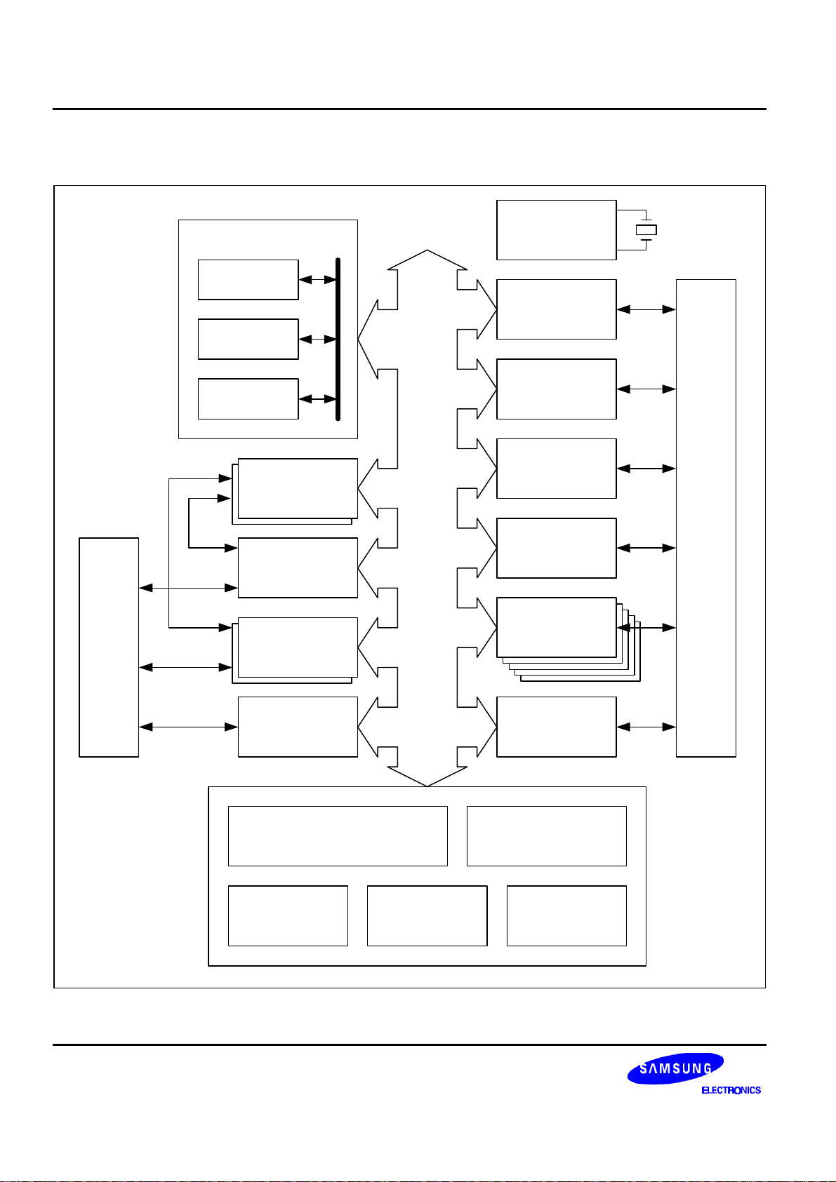
BLOCK DIAGRAM
CPU Unit
Write
Buffer
ARM7TDMI
CPU Core
Cache
4 Kbyte
General Purpose I/O Ports
DMA0,1
UART
SYSTEM BUS
System Clock
Circuit
Basic Timer
&
WDT
A/D
Converter
Interrupt
Controller
Real Time Clock
Generator
Crystal/
Ceramic
Oscillator
Timer 0,1,2,3,4
Serial I/O 0,1
GPIO
Controller
SYSTEM BUS CONTROLLER BUS ARBITRATION
BUS
INTERFACE
Figure 1-1. S3C3410X Block Diagram
ROM/
FLASH/SRAM
CONTROLLER
IIC BUS
FP/DRAM/
SDRAM
CONTROLLER
1-4
Page 9

S3C3410X RISC MICROPROCESSOR PRODUCT OVERVIEW
nCS6:nRAS0:nSCS0/P2.5
nCS7:nRAS1:nSCS1/P2.6
nWBE0:nBE0:DQM0/P3.0
nWBE1:nBE1:DQM1/P3.1
PIN ASSIGNMENTS
AIN3/P8.3
AIN2/P8.2
AIN1/P8.1
AIN0/P8.0
AVREF
ADCVSS
EXTAL1
XTAL1
RTCVDD
TEST1
TEST0
nRESET
EXTAL0
XTAL0
RP7/P7.7
RP6/P7.6
VDD
VSS
RP5/P7.5
TDO/RP4/P7.4
nTRST/RP3/P7.3
TDI/RP2/P7.2
TMS/RP1/P7.1
TCK/RP0/P7.0
EINT3/P6.7
SIOTXD1/P6.6
128
127
126
125
124
123
122
121
120
119
118
117
116
115
114
113
112
111
110
109
108
107
106
105
104
103
AIN4/EINT8/P8.4
AIN5/EINT9/P8.5
AIN6/EINT10/P8.6
AIN7/EINT11/P8.7
ADCVDD
TCLK0/TCAP0/P0.0
TCLK1/TCAP1/P0.1
TCLK2/TCAP2P0.2
VSS
VDD
TCLK3/P0.3
TCLK4/P0.4
TCAP3/TOUT3/PWM0/P0.5
TCAP4/TOUT4/PWM1/P0.6
EINT0/nWREXP/P0.7
A0
A1
A2
VSS
VDD
A3
A4
A5
A6
A7
A8/A16
A9/A17
A10/A18
VSS
VDD
A11/A19
A12/A20
A13/A21
A14/A22
A15/A23
A16/P1.0
A17/P1.1
A18/P1.2
1
2
3
4
5
6
7
8
9
10
11
12
13
14
15
16
17
18
19
20
21
22
23
24
25
26
27
28
29
30
31
32
33
34
35
36
37
38
39404142434445464748495051525354555657585960616263
S3C3410X
(128-QFP-1420)
102
101
100
SIOCLK1/P6.5
SIORXD1/P6.4
SIORDY/nWAIT/P6.3
SIOTXD0/P6.2
99
SIOCLK0/P6.1
98
SIORXD0/P6.0
97
UTXD/P5.7
96
URXD/P5.6
95
VDD
94
VSS
93
IICSCK/P5.5
92
IICSDA/P5.4
91
nDACK1/P5.3
90
nDREQ1/P5.2
89
nDACK0/P5.1
88
nDREQ0/P5.0
87
D15/A23/P4.7
86
D14/A22/P4.6
85
VDD
84
VSS
83
D13/A21/P4.5
82
D12/A20/P4.4
81
D11/A19/P4.3
80
D10/A18/P4.2
79
D9/A17/P4.1
78
D8/A16/P4.0
77
D7
76
D6
75
VDD
74
VSS
73
D5
72
D4
71
D3
70
D2
69
D1
68
D0
67
DCLK/P9.1
66
LP/P9.0
65
64
VSS
A19/P1.3
A20/EINT4/P1.4
A21/EINT5/P1.5
A22/EINT6/P1.6
A23/EINT7/P1.7
nCS0
nCS1/P2.0
nCS2/P2.1
nCS3/P2.2
nCS4/P2.3
nCS5/P2.4
VDD
nAS
nOE
EINT1/nECS0/P2.7
Figure 1-2. S3C3410X Pin Assignments
nWE/P3.4
SCLK/P3.6
SCKE/P3.5
nCAS0:nSRAS/P3.2
nCAS1:nSCAS/P3.3
EINT2/nECS1/P3.7
1-5
Page 10

PRODUCT OVERVIEW S3C3410X RISC MICROPROCESSOR
Table 1-1. 128-Pin QFP Pin Assignment
Pin No Function I/O State @Initial I/O Type Reset
1 AIN4/EINT8/P8.4 I piseuc P8.4
2 AIN5/EINT9/P8.5 I piseuc P8.5
3 AIN6/EINT10/P8.6 I piseuc P8.6
4 AIN7/EINT11/P8.7 I piseuc P8.7
5 ADCVDD P vddt
6 TCLK0/TCAP0/P0.0 IO pbseuct4 P0.0
7 TCLK1/TCAP1/P0.1 IO pbseuct4 P0.1
8 TCLK2/TCAP2/P0.2 IO pbseuct4 P0.2
9 VSS P vss
10 VDD P vdd
11 TCLK3/P0.3 IO pbseuct4 P0.3
12 TCLK4/P0.4 IO pbseuct4 P0.4
13 TCAP3/TOUT3/PWM0/P0.5 IO pbseuct4 P0.5
14 TCAP4/TOUT4/PWM1/P0.6 IO pbseuct4 P0.6
15 EINT0/nWREXP/P0.7 IO pbseuct8 P0.7
16 A0 O pob8 A0
17 A1 O pob8 A1
18 A2 O pob8 A2
19 VSS P vss
20 VDD P vdd
21 A3 O pob8 A3
22 A4 O pob8 A4
23 A5 O pob8 A5
24 A6 O pob8 A6
25 A7 O pob8 A7
26 A8/A16 O pob8 A8
27 A9/A17 O pob8 A9
28 A10/A18 O pob8 A10
29 VSS P vss
30 VDD P vdd
31 A11/A19 O pob8 A11
32 A12/A20 O pob8 A12
1-6
Page 11

S3C3410X RISC MICROPROCESSOR PRODUCT OVERVIEW
Table 1-1. 128-Pin QFP Pin Assignment (Continued)
Pin No Function I/O State @Initial I/O Type Reset
33 A13/A21 O pob8 A13
34 A14/A22 O pob8 A14
35 A15/A23 O pob8 A15
36 A16/P1.0 IO pbcedct8 P1.0
37 A17/P1.1 IO pbcedct8 P1.1
38 A18/P1.2 IO pbcedct8 P1.2
39 A19/P1.3 IO pbcedct8 P1.3
40 A20/EINT4/P1.4 IO pbsedct8 P1.4
41 A21/EINT5/P1.5 IO pbsedct8 P1.5
42 A22/EINT6/P1.6 IO pbsedct8 P1.6
43 A23/EINT7/P1.7 IO pbsedct8 P1.7
44 nCS0 O pob8 nCS0
45 nCS1/P2.0 IO pbceuct8 P2.0
46 nCS2/P2.1 IO pbceuct8 P2.1
47 nCS3/P2.2 IO pbceuct8 P2.2
48 nCS4/P2.3 IO pbceuct8 P2.3
49 nCS5/P2.4 IO pbceuct8 P2.4
50 nCS6:nRAS0:nSCS0/P2.5 IO pbceuct8 P2.5
51 VSS P vss
52 VDD P vdd
53 nCS7:nRAS1:nSCS1/P2.6 IO pbceuct8 P2.6
54 EINT1/nECS0/P2.7 IO pbseuct8 P2.7
55 nOE O pob8 nOE
56 nAS O pob8 nAS
57 nWBE0:nBE0:DQM0/P3.0 IO pbceuct8 P3.0
58 nWBE1:nBE1:DQM1/P3.1 IO pbceuct8 P3.1
59 nCAS0:nSRAS/P3.2 IO pbceuct8 P3.2
60 nCAS1:nSCAS/P3.3 IO pbceuct8 P3.3
61 nWE/P3.4 IO pbceuct8 P3.4
62 SCKE/P3.5 IO pbceuct8 P3.5
63 SCLK/P3.6 IO pbceuct8 P3.6
64 EINT2/nECS1/P3.7 IO pbseuct8 P3.7
1-7
Page 12

PRODUCT OVERVIEW S3C3410X RISC MICROPROCESSOR
Table 1-1. 128-Pin QFP Pin Assignment (Continued)
Pin No Function I/O State @Initial I/O Type Reset
65 LP/P9.0 O pob8 LP
66 DCLK/P9.1 O pob8 DCLK
67 D0 IO pbcedct8 D0
68 D1 IO pbcedct8 D1
69 D2 IO pbcedct8 D2
70 D3 IO pbcedct8 D3
71 D4 IO pbcedct8 D4
72 D5 IO pbcedct8 D5
73 VSS P vss
74 VDD P vdd
75 D6 IO pbcedct8 D6
76 D7 IO pbsedct8 D7
77 D8/A16/P4.0 IO pbcedct8 P4.0
78 D9/A17/P4.1 IO pbcedct8 P4.1
79 D10/A18/P4.2 IO pbcedct8 P4.2
80 D11/A19/P4.3 IO pbcedct8 P4.3
81 D12/A20/P4.4 IO pbcedct8 P4.4
82 D13/A21/P4.5 IO pbcedct8 P4.5
83 VSS P vss
84 VDD P vdd
85 D14/A22/P4.6 IO pbcedct8 P4.6
86 D15/A23/P4.7 IO pbcedct8 P4.7
87 nDREQ0/P5.0 IO pbceuct4 P5.0
88 nDACK0/P5.1 IO pbceuct4 P5.1
89 nDREQ1/P5.2 IO pbceuct4 P5.2
90 nDACK1/P5.3 IO pbceuct4 P5.3
91 IICSDA/P5.4 IO pbceuct8 P5.4
92 IICSCK/P5.5 IO pbceuct8 P5.5
93 VSS P vss
94 VDD P vdd
95 URXD/P5.6 IO pbceuct4 P5.6
96 UTXD/P5.7 IO pbceuct4 P5.7
1-8
Page 13

S3C3410X RISC MICROPROCESSOR PRODUCT OVERVIEW
Table 1-1. 128-Pin QFP Pin Assignment (Continued)
Pin No Function I/O State @Initial I/O Type Reset
97 SIORXD0/P6.0 IO pbseuct4 P6.0
98 SIOCLK0/P6.1 IO pbseuct4 P6.1
99 SIOTXD0/P6.2 IO pbseuct4 P6.2
100 SIORDY/nWAIT/P6.3 IO pbseuct4 P6.3
101 SIORXD1/P6.4 IO pbseuct4 P6.4
102 SIOCLK1/P6.5 IO pbseuct4 P6.5
103 SIOTXD1/P6.6 IO pbseuct4 P6.6
104 EINT3/P6.7 IO pbseuct4 P6.7
105 TCK/RP0/P7.0 IO pbceuct4 P7.0
106 TMS/RP1/P7.1 IO pbceuct4 P7.1
107 TDI/RP2/P7.2 IO pbceuct4 P7.2
108 nTRST/RP3/P7.3 IO pbceuct4 P7.3
109 TDO/RP4/P7.4 IO pbceuct4 P7.4
110 RP5/P7.5 IO pbceuct4 P7.5
111 VSS P vss
112 VDD P vdd
113 RP6/P7.6 IO pbceuct4 P7.6
114 RP7/P7.7 IO pbceuct4 P7.7
115 XTAL0 I oscm XTAL0
116 EXTAL0 O oscm EXTAL0
117
RESET
I pisu
RESET
118 TEST0 I pis TEST0
119 TEST1 I pis TEST1
120 RTCVDD P vddt
121 XTAL1 I oscm XTAL1
122 EXTAL1 O oscm EXTAL1
123 ADCVSS P vsst
124 AVREF A apad AVREF
125 AIN0/P8.0 I piseuc P8.0
126 AIN1/P8.1 I piseuc P8.1
127 AIN2/P8.2 I piseuc P8.2
128 AIN3/P8.3 I piseuc P8.3
1-9
Page 14

PRODUCT OVERVIEW S3C3410X RISC MICROPROCESSOR
Table 1-2. I/O Type Description
I/O Type Description
vdd, vss 3.3V Vdd/Vss
vddt, vsst 3.3V Vdd/Vss for analog circuitry
pbceuct4 bi-direction pad, CMOS level, pull-up resister with control, tri-state, Io = 4mA
pbseuct4 bi-direction pad, CMOS schmitt-trigger, pull-up resister with control, tri-state, Io = 4mA
pbceuct8 bi-direction pad, CMOS level, pull-up resister with control, tri-state, Io = 8mA
pbseuct8 bi-direction pad, CMOS schmitt-trigger, pull-up resister with control, tri-state, Io = 8mA
pbcedct8 bi-direction pad, CMOS level, pull-down resister with control, tri-state, Io = 8mA
pbsedct8 bi-direction pad, CMOS schmitt-trigger, pull-down resister with control, tri-state, Io = 8mA
pob8 output pad, Io = 8mA
pis input pad, CMOS schmitt-trigger
pisu input pad, CMOS schmitt-trigger, pull-up resister
piceuc input pad, CMOS level, pull-up resister with control
piseuc input pad, CMOS schmitt-trigger, pull-up resister with control
apad pad for analog pin
oscm pad for x-tal oscillation
1-10
Page 15

S3C3410X RISC MICROPROCESSOR PRODUCT OVERVIEW
PIN DESCRIPTIONS
Table 1-3. S3C3410X Pin Descriptions
Pin I/O Description
BUS CONTROLLER
TEST[1:0] I The TEST[1:0] can configure the data bus size for bank 0 in normal or MDS mode.
The normal mode is for CPU to start its operation by fetching the instruction from
external memory. The MDS mode is for CPU to be debugged by the external
Emulator, EmbeddedICE, etc.
00 = Normal mode with 8-bit data bus size for bank 0 access.
01 = Normal mode with 16-bit data bus size for bank 0 access.
10 = MDS mode with 8-bit data bus size for bank 0 access.
11 = MDS mode with 16-bit data bus size for bank 0 access.
A[23:0] O A[23:0] (address bus) generate the address when external memory access.
D[15:0] I/O D[15:0] (Data bus) input the data during memory read and output the data during
memory write. The data bus width can be programmable for 8-bit or 16-bit by the
BANKCONx register option.
nCS[7:0] O nCS[7:0] (Chip Select) selectively generate the chip select signal of each bank when
the external memory access address is within the address range of each bank. The
number of access cycle and the bank size can be programmable by the BANKCONx
register option.
nECS[1:0] O nECS[1:0] (External Chip Select) generate the external chip select signal for the
extra device (External I/O device).
nOE O nOE (Output Enable) indicates that the current bus cycle is a read cycle.
nWE O nWE (Write Enable for x16 SRAM or SDRAM) indicates that the current bus cycle is
a write cycle. To support the byte write to external memory, the byte to be accessed
can be determined by nBE[1:0], which is the selection on upper byte or lower byte.
For example, in case of 16-bit SRAM, nBE[1:0] should play it role as UB(Upper
Byte)/LB(Lower Byte) to select the upper byte or lower byte. In case of SDRAM,
nWBE[1:0] should play it role as DQM[1:0] to select the upper byte or lower byte. For
16-bit access, not 8-bit access, both nWBE[1:0] should be activated at same time. In
certain case, no more byte access is needed. For example, x16 Flash Memory does
not need byte access through 16-bit bus when user need the programming in the
flash memory. In this case, please use nWBE[0] instead of nWE to indicate that the
current bus cycle is a write cycle. Summarizing, nWE should be used to indicate the
write bus cycle in case of x16 SRAM and x16/x8 SDRAM. In case of x16 with two x8
SRAM, nWBE[0] and nWBE[1] should be connected to the WE of SRAM,
respectively. For more detail information, please refer the chapter 4.
nWBE[1:0] O nWBE[1:0] (Write Byte Enable). In case of Flash or ROM access, nWBE[0] should
be connected to the WE of memory. For the access to the non-volatile memory, we
do not need the selection on bytes because the 8-bit write cycle via 16-bit bus is no
more necessary. To program the data into the non-volatile memory, we should
always use the 16-bit access. In this configuration, please use nWBE[0] instead of
nWE to indicate that the current bus cycle is a write cycle. Summarizing, nWBE[0]
should be used to indicate the current write bus cycle in case of x8 SRAM, x8/x16
ROM, EDODRAM or Flash memory. For more detail information, please refer the
chapter 4.
1-11
Page 16

PRODUCT OVERVIEW S3C3410X RISC MICROPROCESSOR
Table 1-3. S3C3410X Signal Descriptions (Continued)
Pin I/O Description
nAS O nAS generates an address strobe signal for latch device in multiplexed address
mode which generate A[23:16] and A[15:8] address in A[15:8] pins.
nWAIT I nWAIT receives request signal to prolong a current bus cycle. As long as nWAIT is
"Low", the current bus cycle cannot be completed.
nWREXP O nWREXP outputs write strobe signal for external device, when you write any data
into EXTPORT register to interface external device.
DRAM/SDRAM
nRAS[1:0] O Row Address Strobe
nCAS[1:0] O Column Address Strobe
nSCS[1:0] O SDRAM Chip Select
nSRAS O SDRAM Row Address Strobe
nSCAS O SDRAM Column Address Strobe
DQM[1:0] O SDRAM Data Mask
SCLK O SDRAM Clock
SCKE O SDRAM Clock Enable
16-bit/8-bit Timer
TCLK[4:0] I External clock input for Timer
TCAP[4:0] I Capture input for Timer
TOUT[4:3] O Timer 3, 4 output or PWM output
DMA
nDREQ[1:0] I External DMA request
nDACK[1:0] O External DMA acknowledge
Interrupt Controller
EINT[12:0] I External interrupt request
UART
URXD I UART receives data input
UTXD O UART transmits data output
SIO
SIOCLK[1:0] I/O SIO external clock
SIORXD[1:0] I SIO receives data input
SIOTXD[1:0] O SIO transmits data output
SIORDY I/O SIO handshakes signal when SIO operation is done by DMA
IIC-BUS
IICSDA I/O IIC-bus data
IICSCK I/O IIC-bus Clock
1-12
Page 17

S3C3410X RISC MICROPROCESSOR PRODUCT OVERVIEW
Table 1-3. S3C3410X Signal Descriptions (Continued)
Pin I/O Description
ADC
AIN[7:0] A ADC input
AVREF A ADC Vref
General Purpose I/O
Pn.x I/O General purpose input/output ports
RP[7:0] O Real time buffer output ports (refer to P7)
RESET & Clock
RESET
I
RESET is the global reset input for the S3C3410X. For a system reset, RESET must
be held to "Low" level for at least 1us.
XTAL0 A Crystal input for internal oscillation circuit for system clock
EXTAL0 A Crystal output for internal oscillation circuit for system clock. It's the inverted output
of XTAL0.
XTAL1 A 32.768KHz crystal input for RTC
EXTAL1 A 32.768KHz crystal output for RTC. It's the inverted output of XTAL1.
LCD Interface
LP O LCD Line Pulse (Inversion of nECS0)
DCLK O LCD Clock (Inversion of nWREXP)
JTAG Test Logic
nTRST I nTRST (TAP Controller Reset) can reset the TAP controller at power-up. A 100K
pull-up resistor is connected to nTRST pin, internally. If the debugger(BlackICE) is
not used, nTRST pin should be "Low" level or low active pulse should be applied
before CPU running. For example, RESET signal can be tied with nTRST.
TMS I TMS (TAP Controller Mode Select) can control the sequence of the state diagram of
TAP controller. A 100K pull-up resistor is connected to TMS pin, internally.
TCK I TCK (TAP Controller Clock) can provide the clock input for the JTAG logic. A 100K
pull-up resistor is connected to TCK pin, internally.
TDI I TDI (TAP Controller Data Input) is the serial input for JTAG port. A 100K pull-up
resistor is connected to TDI pin, internally.
TDO O TDO (TAP Controller Data Output) is the serial output for JTAG port.
POWER
VDD P Power supply pin
VSS P Ground pin
RTCVDD P RTC power supply
ADCVDD P ADC power supply
ADCVSS P ADC ground & RTC ground
1-13
Page 18

PRODUCT OVERVIEW S3C3410X RISC MICROPROCESSOR
S3C3410X SPECIAL FUNCTION REGISTER
Table 1-4. S3C3410X Special Function Register
Group Register Offset R/W Description AccessReset Value
System SYSCFG0 0x1000 R/W System Configuration Register W 0xfff1
Manager BANKCON0 0x2000 R/W Memory Bank 0 Control Register W 0x00200070
BANKCON1 0x2004 R/W Memory Bank 1 Control Register W 0x0
BANKCON2 0x2008 R/W Memory Bank 2 Control Register W 0x0
BANKCON3 0x200c R/W Memory Bank 3 Control Register W 0x0
BANKCON4 0x2010 R/W Memory Bank 4 Control Register W 0x0
BANKCON5 0x2014 R/W Memory Bank 5 Control Register W 0x0
BANKCON6 0x2018 R/W Memory Bank 6 Control Register W 0x0
BANKCON7 0x201c R/W Memory Bank 7 Control Register W 0x0
REFCON 0x2020 R/W DRAM Refresh Control Register W 0x1
EXTCON0 0x2030 R/W Extra device control register 0 W 0x0
EXTCON1 0x2034 R/W Extra device control register 1 W 0x0
EXTPORT 0x203e R/W External port data register B/H 0x0
EXTDAT0 0x202c R/W Extra chip selection data register 0 B/H 0x0
EXTDAT1 0x202e R/W Extra chip selection data register 1 B/H 0x0
DMA DMACON0 0x300c R/W DMA 0 control register W 0x0
DMASRC0 0x3000 R/W DMA 0 source address register W 0x0
DMADST0 0x3004 R/W DMA 0 destination address register W 0x0
DMACNT0 0x3008 R/W DMA 0 transfer count register W 0x0
DMACON1 0x400c R/W DMA 1 Control Register W 0x0
DMASRC1 0x4000 R/W DMA 1 source address register W 0x0
DMADST1 0x4004 R/W DMA 1 destination address register W 0x0
DMACNT1 0x4008 R/W DMA 1 transfer count register W 0x0
I/O Port PDAT0 0xb000 R/W Port 0 data register B 0x0
PDAT1 0xb001 R/W Port 1 data register B 0x0
PDAT2 0xb002 R/W Port 2 data register B 0x0
PDAT3 0xb003 R/W Port 3 data register B 0x0
PDAT4 0xb004 R/W Port 4 data register B 0x0
PDAT5 0xb005 R/W Port 5 data register B 0x0
PDAT6 0xb006 R/W Port 6 data register B 0x0
PDAT7 0xb007 R/W Port 7 data register B 0x0
PDAT8 0xb008 R Port 8 data register B 0x0
1-14
Page 19
S3C3410X RISC MICROPROCESSOR PRODUCT OVERVIEW
Table 1-4. S3C3410X Special Function Register (Continued)
Group Register Offset R/W Description Access Reset Value
I/O Port PDAT9 0xb009 R/W Port 9 data register B 0x0
P7BR 0xb00b R/W Port 7 buffer register B 0x0
PCON0 0xb010 R/W Port 0 control register H 0x0
PCON1 0xb012 R/W Port 1 control register H 0x0
PCON2 0xb014 R/W Port 2 control register H 0x0
PCON3 0xb016 R/W Port 3 control register H 0x0
PCON4 0xb018 R/W Port 4 control register H 0x0
PCON5 0xb01c R/W Port 5 control register W 0x0
PCON6 0xb020 R/W Port 6 control register W 0x0
PCON7 0xb024 R/W Port 7 control register H 0x0
PCON8 0xb026 R/W Port 8 control register B 0x0
PCON9 0xb027 R/W Port 9 control register B 0x0
PUR0 0xb028 R/W Port 0 pull-up control register B 0x80
PDR1 0xb029 R/W Port 1 pull-down control register B 0xff
PUR2 0xb02a R/W Port 2 pull-up control register B 0xff
PUR3 0xb02b R/W Port 3 pull-up control register B 0xff
PDR4 0xb02c R/W Port 4 pull-down control register B 0xff
PUR5 0xb02d R/W Port 5 pull-up control register B 0x0
PUR6 0xb02e R/W Port 6 pull-up control register B 0x0
PUR7 0xb02f R/W Port 7 pull-up control register B 0x0
PUR8 0xb03c R/W Port 8 pull-up control register B 0x0
EINTPND 0xb031 R/W External interrupt pending register B 0x0
EINTCON 0xb032 R/W External interrupt control register H 0x0
EINTMOD 0xb034 R/W External interrupt mode register W 0x0
Timer 0 TDAT0 0x9000 R/W Timer 0 data register H 0xffff
TPRE0 0x9002 R/W Timer 0 prescaler register B 0x0
TCON0 0x9003 R/W Timer 0 control register B 0x0
TCNT0 0x9006 R Timer 0 counter register H 0x0
Timer 1 TDAT1 0x9010 R/W Timer 1 data register H 0xffff
TPRE1 0x9012 R/W Timer 1 prescaler register B 0x0
TCON1 0x9013 R/W Timer 1 control register B 0x0
TCNT1 0x9016 R Timer 1 counter register H 0x0
1-15
Page 20
PRODUCT OVERVIEW S3C3410X RISC MICROPROCESSOR
Table 1-4. S3C3410X Special Function Register (Continued)
Group Register Offset R/W Description Access Reset Value
Timer 2 TDAT2 0x9020 R/W Timer 2 data register H 0xffff
TPRE2 0x9022 R/W Timer 2 prescaler register B 0x0
TCON2 0x9023 R/W Timer 2 control register B 0x0
TCNT2 0x9026 R Timer 2 counter register H 0x0
Timer 3 TDAT3 0x9031 R/W Timer 3 data register B 0xff
TPRE3 0x9032 R/W Timer 3 prescaler register B 0x0
TCON3 0x9033 R/W Timer 3 control register B 0x0
TCNT3 0x9037 R Timer 3 counter register B 0x0
Timer 4 TDAT4 0x9041 R/W Timer 4 data register B 0xff
TPRE4 0x9042 R/W Timer 4 prescaler register B 0x0
TCON4 0x9043 R/W Timer 4 control register B 0x0
TCNT4 0x9047 R Timer 4 counter register B 0x0
TFCON 0x904f R/W FIFO control register of Timer 4 B 0x0
TFSTAT 0x904e R FIFO status register of Timer 4 B 0x0
TFB4 0x904b R/W Timer 4 FIFO register @ byte B 0x0
TFHW4 0x904a R/W Timer 4 FIFO register @ half-word H 0x0
TFW4 0x9048 R/W Timer 4 FIFO register @ word W 0x0
UART ULCON 0x5003 R/W UART line control register B 0x0
UCON 0x5007 R/W UART control register B 0x0
USTAT 0x500b R UART status register B 0x0
UFCON 0x500f R/W UART FIFO control register B 0x0
UFSTAT 0x5012 R UART FIFO status register B 0x0
UTXH 0x5017 R/W UART transmit holding register B 0x0
UTXH_B 0x5017 R/W UART transmit FIFO register @ byte B 0x0
UTXH_HW 0x5016 R/W UART transmit FIFO register
H 0x0
@ half-word
UTXH_W 0x5014 R/W UART transmit FIFO register @ word W 0x0
URXH 0x501b R/W UART receive buffer register B 0x0
URXH_B 0x501b R/W UART receive FIFO register @ byte B 0x0
URXH_HW 0x501a R/W UART receive FIFO register
H 0x0
@ half-word
URXH_W 0x5018 R/W UART receive FIFO register @ word W 0x0
UBRDIV 0x501e R/W Baud rate divisor register for UART H 0x0
1-16
Page 21

S3C3410X RISC MICROPROCESSOR PRODUCT OVERVIEW
Table 1-4. S3C3410X Special Function Register (Continued)
Group Register Offset R/W Description Access Reset Value
SIO 0 ITVCNT0 0x6000 R/W SIO 0 interval counter register B 0x0
SBRDR0 0x6001 R/W SIO 0 baud rate prescaler register B 0x0
SIODAT0 0x6002 R/W SIO 0 data register B 0x0
SIOCON0 0x6003 R/W SIO 0 control register B 0x0
SIO 1 ITVCNT1 0x7000 R/W SIO 1 interval counter register B 0x0
SBRDR1 0x7001 R/W SIO 1 baud rate prescaler register B 0x0
SIODAT1 0x7002 R/W SIO 1 data register B 0x0
SIOCON1 0x7003 R/W SIO 1 control register B 0x0
Interrupt INTMOD 0xc000 R/W Interrupt mode register W 0x0
INTPND 0xc004 R/W Interrupt pending register W 0x0
INTMSK 0xc008 R/W Interrupt mask register W 0x0
INTPRI0 0xc00c R/W Interrupt priority register 0 W 0x03020100
INTPRI1 0xc010 R/W Interrupt priority register 1 W 0x07060504
INTPRI2 0xc014 R/W Interrupt priority register 2 W 0x0b0a0908
INTPRI3 0xc018 R/W Interrupt priority register 3 W 0x0f0e0d0c
INTPRI4 0xc01c R/W Interrupt priority register 4 W 0x13121110
INTPRI5 0xc020 R/W Interrupt priority register 5 W 0x17161514
INTPRI6 0xc024 R/W Interrupt priority register 6 W 0x1b1a1918
INTPRI7 0xc028 R/W Interrupt priority register 7 W 0x1f1e1d1c
ADC ADCCON 0x8002 R/W A/D Converter control register H 0x140
ADCDAT 0x8006 R A/D Converter data register H 0x0
Basic BTCON 0xa002 R/W Basic Timer control register H 0x0
Timer BTCNT 0xa007 R Basic Timer count register B 0x0
IIC IICCON 0xe000 R/W IIC-bus control register B 0x0
IICSTAT 0xe001 R/W IIC-bus status register B 0x0
IICDS 0xe002 R/W IIC-Bus transmit/receive data shift
B 0x0
register
IICADD 0xe003 R/W IIC-Bus transmit/receive address
B 0x0
register
IICPS 0xe004 R/W IIC-Bus Prescaler register B 0x0
IICPCNT 0xe005 R/W IIC-Bus Prescaler Counter register B 0x0
SYSON 0xd003 R/W System control register B 0x0
1-17
Page 22

PRODUCT OVERVIEW S3C3410X RISC MICROPROCESSOR
Table 1-4. S3C3410X Special Function Register (Continued)
Group Register Offset R/W Description Access Reset Value
RTC RTCCON 0xa013 R/W RTC control register B 0x0
RTCALM 0xa012 R/W RTC alarm control register B 0x0
ALMSEC 0xa033 R/W Alarm second data register B 0x59
ALMMIN 0xa032 R/W Alarm minute data register B 0x59
ALMHOUR 0xa031 R/W Alarm hour data register B 0x23
ALMDAY 0xa037 R/W Alarm day data register B 0x31
ALMMON 0xa036 R/W Alarm month data register B 0x12
ALMYEAR 0xa035 R/W Alarm year data register B 0x99
BCDSEC 0xa023 R/W BCD second data register B –
BCDMIN 0xa022 R/W BCD minute data register B –
BCDHOUR 0xa021 R/W BCD hour data register B –
BCDDAY 0xa027 R/W BCD day data register B –
BCDDATE 0xa020 R/W BCD date data register B –
BCDMON 0xa026 R/W BCD month data register B –
BCDYEAR 0xa025 R/W BCD year data register B –
RINTPND 0xa010 R/W RTC time interrupt pending register B 0x0
RINTCON 0xa011 R/W RTC time interrupt control register B 0x0
1-18
Page 23

S3C3410X RISC MICROPROCESSOR PROGRAMMER'S MODEL
2 PROGRAMMER'S MODEL
OVERVIEW
S3C3410X was developed using the advanced ARM7TDMI core designed by Advanced RISC Machines, Ltd.
ARM7TDMI supports big-endian and little-endian memory formats, but the S3C3410X supports only the bigendian memory format.
PROCESSOR OPERATING STATES
From the programmer's point of view, the ARM7TDMI can be in one of two states:
• ARM state which executes 32-bit, word-aligned ARM instructions.
• THUMB state which operates with 16-bit, halfword-aligned THUMB instructions. In this state, the PC uses bit
1 to select between alternate halfwords.
NOTE
Transition between these two states does not affect the processor mode or the contents of the registers.
SWITCHING STATE
Entering THUMB State
Entry into THUMB state can be achieved by executing a BX instruction with the state bit (bit 0) set in the operand
register.
Transition to THUMB state will also occur automatically on return from an exception (IRQ, FIQ, UNDEF, ABORT,
SWI etc.), if the exception was entered with the processor in THUMB state.
Entering ARM State
Entry into ARM state happens:
• On execution of the BX instruction with the state bit clear in the operand register.
• On the processor taking an exception (IRQ, FIQ, RESET, UNDEF, ABORT, SWI etc.). In this case, the PC is
placed in the exception mode's link register, and execution commences at the exception's vector address.
MEMORY FORMATS
ARM7TDMI views memory as a linear collection of bytes numbered upwards from zero. Bytes 0 to 3 hold the first
stored word, bytes 4 to 7 the second and so on. ARM7TDMI can treat words in memory as being stored either in
Big-Endian or Little-Endian format.
2-1
Page 24
PROGRAMMER'S MODEL S3C3410X RISC MICROPROCESSOR
BIG-ENDIAN FORMAT
In Big-Endian format, the most significant byte of a word is stored at the lowest numbered byte and the least
significant byte at the highest numbered byte. Byte 0 of the memory system is therefore connected to data lines
31 through 24.
Higher Address
Lower Address
31
8
4
0
Most significant byte is at lowest address.
Word is addressed by byte address of most significant byte.
23
24 1516
9
5
1
10
6
2
8 7 0
11
7
3
Word Address
8
4
0
Figure 2-1. Big-Endian Addresses of Bytes within Words
LITTLE-ENDIAN FORMAT
In Little-Endian format, the lowest numbered byte in a word is considered the word's least significant byte, and
the highest numbered byte the most significant. Byte 0 of the memory system is therefore connected to data lines
7 through 0.
Higher Address
31 23 8 7 0
24 1516
Word Address
8
4
0
Lower Address
11
7
3
Least significant byte is at lowest address.
Word is addressed by byte address of least significant byte.
10
6
2
9
5
1
8
4
0
Figure 2-2. Little-Endian Addresses of Bytes whthin Words
INSTRUCTION LENGTH
Instructions are either 32 bits long (in ARM state) or 16 bits long (in THUMB state).
Data Types
ARM7TDMI supports byte (8-bit), halfword (16-bit) and word (32-bit) data types. Words must be aligned to fourbyte boundaries and half words to two-byte boundaries.
2-2
Page 25

S3C3410X RISC MICROPROCESSOR PROGRAMMER'S MODEL
OPERATING MODES
ARM7TDMI supports seven modes of operation:
• User (usr): The normal ARM program execution state
• FIQ (fiq): Designed to support a data transfer or channel process
• IRQ (irq): Used for general-purpose interrupt handling
• Supervisor (svc): Protected mode for the operating system
• Abort mode (abt): Entered after a data or instruction prefetch abort
• System (sys): A privileged user mode for the operating system
• Undefined (und): Entered when an undefined instruction is executed
Mode changes may be made under software control, or may be brought about by external interrupts or exception
processing. Most application programs will execute in User mode. The non-user modes' known as privileged
modes-are entered in order to service interrupts or exceptions, or to access protected resources.
REGISTERS
ARM7TDMI has a total of 37 registers - 31 general-purpose 32-bit registers and six status registers - but these
cannot all be seen at once. The processor state and operating mode dictate which registers are available to the
programmer.
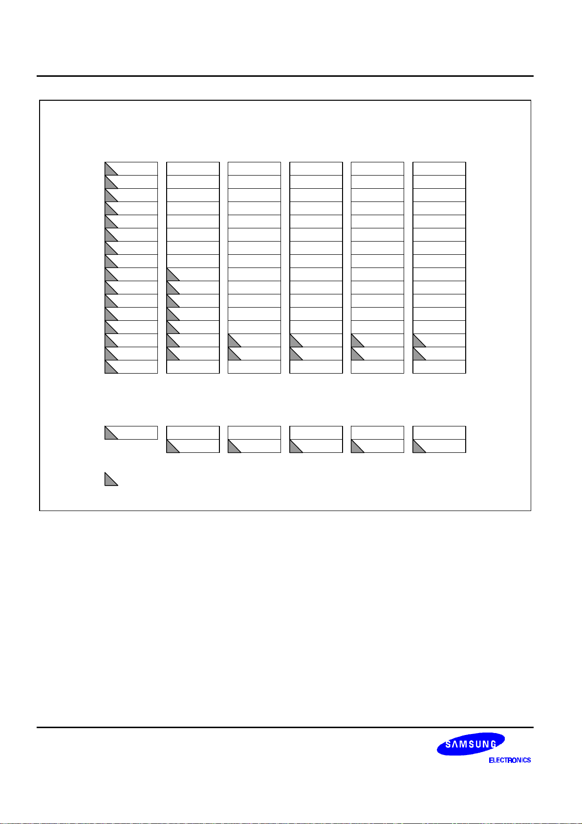
The ARM State Register Set
In ARM state, 16 general registers and one or two status registers are visible at any one time. In privileged (nonUser) modes, mode-specific banked registers are switched in. Figure 2-3 shows which registers are available in
each mode: the banked registers are marked with a shaded triangle.
The ARM state register set contains 16 directly accessible registers: R0 to R15. All of these except R15 are
general-purpose, and may be used to hold either data or address values. In addition to these, there is a
seventeenth register used to store status information.
Register 14 is used as the subroutine link register. This receives a copy of R15 when a Branch
and Link (BL) instruction is executed. At all other times it may be treated as a
general-purpose register. The corresponding banked registers R14_svc, R14_irq,
R14_fiq, R14_abt and R14_und are similarly used to hold the return values of R15
when interrupts and exceptions arise, or when Branch and Link instructions are
executed within interrupt or exception routines.
Register 15 holds the Program Counter (PC). In ARM state, bits [1:0] of R15 are zero and bits
[31:2] contain the PC. In THUMB state, bit [0] is zero and bits [31:1] contain the PC.
Register 16 is the CPSR (Current Program Status Register). This contains condition code flags
and the current mode bits.
FIQ mode has seven banked registers mapped to R8-14 (R8_fiq-R14_fiq). In ARM state, many FIQ handlers do
not need to save any registers. User, IRQ, Supervisor, Abort and Undefined each have two banked registers
mapped to R13 and R14, allowing each of these modes to have a private stack pointer and link registers.
2-3
Page 26
PROGRAMMER'S MODEL S3C3410X RISC MICROPROCESSOR
ARM State General Registers and Program Counter
User/System
R0
R1
R2
R3
R4
R5
R6
R7
R8
R9
R10
R11
R12
R13
R14
R15 (PC)
CPSR CPSR
FIQ
R0
R1
R2
R3
R4
R5
R6
R7
R8_fiq
R9_fiq
R10_fiq
R11_fiq
R12_fiq
R13_fiq
R14_fiq
R15 (PC)
Supervisor IRQAbort Undefined
R0
R1
R2
R3
R4
R5
R6
R7
R8
R9
R10
R11
R12
R13_svc
R14_svc
R15 (PC)
R0
R1
R2
R3
R4
R5
R6
R7
R8
R9
R10
R11
R12
R13_abt
R14_abt
R15 (PC)
ARM State Program Status Registers
CPSR
SPSR_abt
SPSR_fiq
CPSR
SPSR_svc
R0
R1
R2
R3
R4
R5
R6
R7
R8
R9
R10
R11
R12
R13_irq
R14_irq
R15 (PC)
CPSR
SPSR_irq
R0
R1
R2
R3
R4
R5
R6
R7
R8
R9
R10
R11
R12
R13_und
R14_und
R15 (PC)
CPSR
SPSR_und
2-4
= banked register
Figure 2-3. Register Organization in ARM State
Page 27
S3C3410X RISC MICROPROCESSOR PROGRAMMER'S MODEL
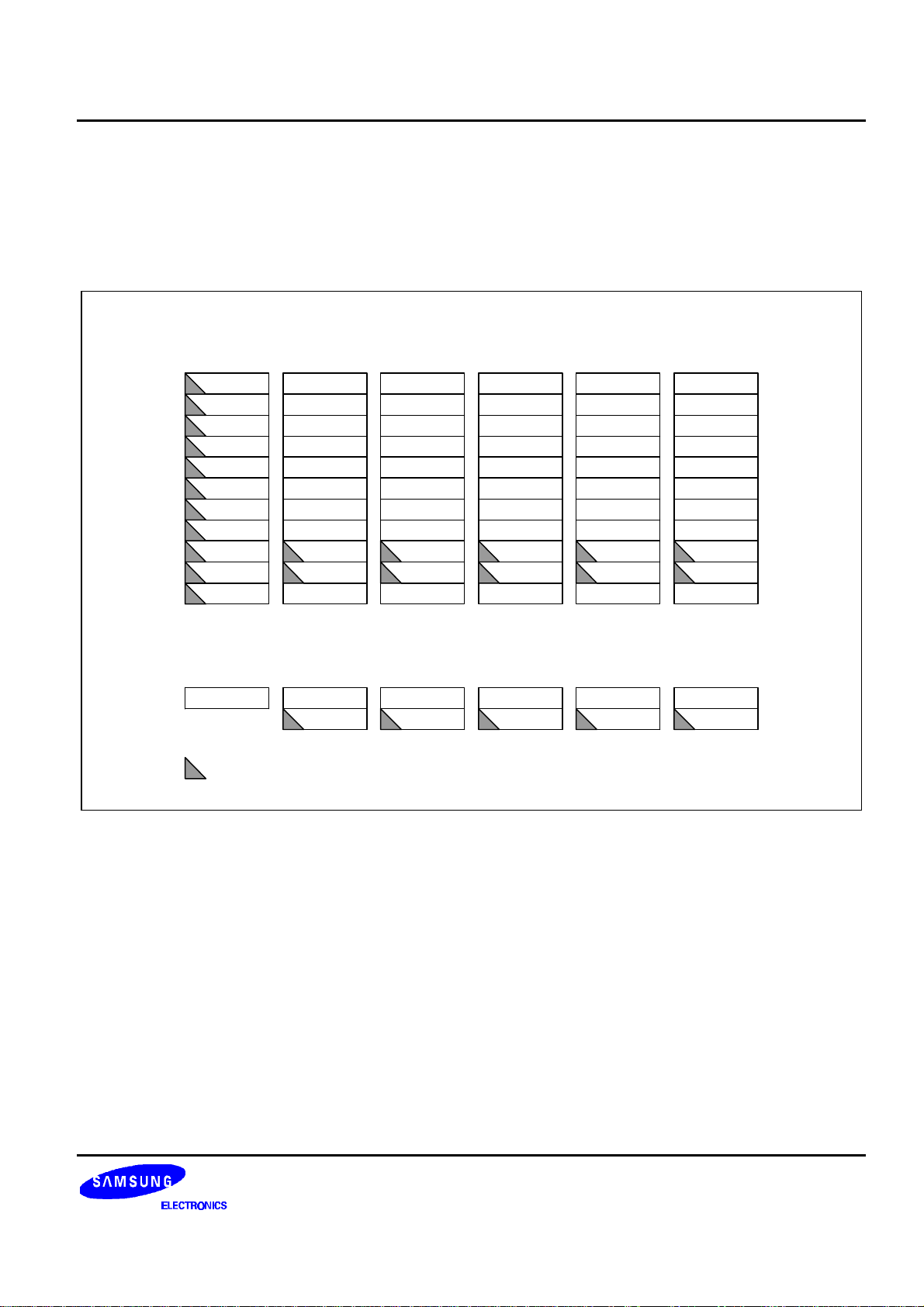
The THUMB State Register Set
The THUMB state register set is a subset of the ARM state set. The programmer has direct access to eight
general registers, R0-R7, as well as the Program Counter (PC), a stack pointer register (SP), a link register (LR),
and the CPSR. There are banked Stack Pointers, Link Registers and Saved Process Status Registers (SPSRs)
for each privileged mode. This is shown in Figure 2-4.
THUMB State General Registers and Program Counter
User/System
R0
R1
R2
R3
R4
R5
R6
R7
SP
LR
PC
CPSR CPSR
= banked register
FIQ
R0
R1
R2
R3
R4
R5
R6
R7
SP_fiq
LR_fiq
PC
Supervisor IRQAbort Undefined
R0
R1
R2
R3
R4
R5
R6
R7
SP_svc
LR_svc
PC
R0
R1
R2
R3
R4
R5
R6
R7
SP_abt
LR_abt
PC
THUMB State Program Status Registers
SPSR_fiq
CPSR
SPSR_svc
CPSR
SPSR_abt
R0
R1
R2
R3
R4
R5
R6
R7
SP_und
LR_und
PC
CPSR
SPSR_irq
R0
R1
R2
R3
R4
R5
R6
R7
SP_fiq
LR_fiq
PC
CPSR
SPSR_und
Figure 2-4. Register Organization in THUMB state
2-5
Page 28

PROGRAMMER'S MODEL S3C3410X RISC MICROPROCESSOR
Lo-registersHi-registers
The relationship between ARM and THUMB state registers
The THUMB state registers relate to the ARM state registers in the following way:
• THUMB state R0-R7 and ARM state R0-R7 are identical
• THUMB state CPSR and SPSRs and ARM state CPSR and SPSRs are identical
• THUMB state SP maps onto ARM state R13
• THUMB state LR maps onto ARM state R14
• The THUMB state Program Counter maps onto the ARM state Program Counter (R15)
This relationship is shown in Figure 2-5.
THUMB state ARM state
R0
R1
R2
R3
R4
R5
R6
R7
Stack Pointer (SP)
Link register (LR)
Program Counter (PC)
CPSR
SPSR
R0
R1
R2
R3
R4
R5
R6
R7
R8
R9
R10
R11
R12
Stack Pointer (R13)
Link register (R14)
Program Counter (R15)
CPSR
SPSR
2-6
Figure 2-5. Mapping of THUMB State Registers onto ARM State Registers
Page 29

S3C3410X RISC MICROPROCESSOR PROGRAMMER'S MODEL
Accessing Hi-Registers in THUMB State
In THUMB state, registers R8-R15 (the Hi registers) are not part of the standard register set. However, the
assembly language programmer has limited access to them, and can use them for fast temporary storage.
A value may be transferred from a register in the range R0-R7 (a Lo register) to a Hi register, and from a Hi
register to a Lo register, using special variants of the MOV instruction. Hi register values can also be compared
against or added to Lo register values with the CMP and ADD instructions. For more information, refer to Figure
3-34.
THE PROGRAM STATUS REGISTERS
The ARM7TDMI contains a Current Program Status Register (CPSR), plus five Saved Program Status Registers
(SPSRs) for use by exception handlers. These register's functions are:
• Hold information about the most recently performed ALU operation
• Control the enabling and disabling of interrupts
• Set the processor operating mode
The arrangement of bits is shown in Figure 2-6.
Condition Code Flags
31
30 29 2728 26 25 24 23 8 7 6 5 4 3 2 1 0
N Z C V I F T M4 M3 M2 M1 M0
Overflow
Carry/Borrow/Extend
Zero
Negative/Less Than
(Reserved) Control Bits
~
~
~
~
Mode bits
State bit
FIQ disable
IRQ disable
Figure 2-6. Program Status Register Format
2-7
Page 30

PROGRAMMER'S MODEL S3C3410X RISC MICROPROCESSOR
The Condition Code Flags
The N, Z, C and V bits are the condition code flags. These may be changed as a result of arithmetic and logical
operations, and may be tested to determine whether an instruction should be executed.
In ARM state, all instructions may be executed conditionally: see Table 3-2 for details.
In THUMB state, only the Branch instruction is capable of conditional execution: see Figure 3-46 for details.
The Control Bits
The bottom 8 bits of a PSR (incorporating I, F, T and M[4:0]) are known collectively as the control bits. These will
be changed when an exception arises. If the processor is operating in a privileged mode, they can also be
manipulated by software.
The T bit
This reflects the operating state. When this bit is set, the processor is executing in THUMB
state, otherwise it is executing in ARM state. This is reflected on the TBIT external signal.
Note that the software must never change the state of the TBIT in the CPSR. If this
happens, the processor will enter an unpredictable state.
Interrupt disable bits
The I and F bits are the interrupt disable bits. When set, these disable the IRQ and FIQ
interrupts respectively.
The mode bits
The M4, M3, M2, M1 and M0 bits (M[4:0]) are the mode bits. These determine the
processor's operating mode, as shown in Table 2-1. Not all combinations of the mode bits
define a valid processor mode. Only those explicitly described shall be used. The user
should be aware that if any illegal value is programmed into the mode bits, M[4:0], then the
processor will enter an unrecoverable state. If this occurs, reset should be applied.
Reserved bits The remaining bits in the PSRs are reserved. When changing a PSR's flag or control bits,
you must ensure that these unused bits are not altered. Also, your program should not rely
on them containing specific values, since in future processors they may read as one or
zero.
2-8
Page 31

S3C3410X RISC MICROPROCESSOR PROGRAMMER'S MODEL
Table 2-1. PSR Mode Bit Values
M[4:0] Mode Visible THUMB state registers Visible ARM state registers
10000 User R7..R0,
LR, SP
R14..R0,
PC, CPSR
PC, CPSR
10001 FIQ R7..R0,
LR_fiq, SP_fiq
PC, CPSR, SPSR_fiq
10010 IRQ R7..R0,
LR_irq, SP_irq
PC, CPSR, SPSR_irq
10011 Supervisor R7..R0,
LR_svc, SP_svc,
PC, CPSR, SPSR_svc
10111 Abort R7..R0,
LR_abt, SP_abt,
PC, CPSR, SPSR_abt
11011 Undefined R7..R0
LR_und, SP_und,
PC, CPSR, SPSR_und
11111 System R7..R0,
LR, SP
R7..R0,
R14_fiq..R8_fiq,
PC, CPSR, SPSR_fiq
R12..R0,
R14_irq, R13_irq,
PC, CPSR, SPSR_irq
R12..R0,
R14_svc, R13_svc,
PC, CPSR, SPSR_svc
R12..R0,
R14_abt, R13_abt,
PC, CPSR, SPSR_abt
R12..R0,
R14_und, R13_und,
PC, CPSR
R14..R0,
PC, CPSR
PC, CPSR
Reserved bits The remaining bits in the PSR's are reserved. When changing a PSR's flag or control bits,
you must ensure that these unused bits are not altered. Also, your program should not rely
on them containing specific values, since in future processors they may read as one or
zero.
2-9
Page 32

PROGRAMMER'S MODEL S3C3410X RISC MICROPROCESSOR
EXCEPTIONS
Exceptions arise whenever the normal flow of a program has to be halted temporarily, for example to service an
interrupt from a peripheral. Before an exception can be handled, the current processor state must be preserved
so that the original program can resume when the handler routine has finished.
It is possible for several exceptions to arise at the same time. If this happens, they are dealt with in a fixed order.
See Exception Priorities on page 2-14.
Action on Entering an Exception
When handling an exception, the ARM7TDMI:
1. Preserves the address of the next instruction in the appropriate Link Register. If the exception has been
entered from ARM state, then the address of the next instruction is copied into the Link Register (that is,
current PC + 4 or PC + 8 depending on the exception. See Table 2-2 on for details). If the exception has
been entered from THUMB state, then the value written into the Link Register is the current PC offset by a
value such that the program resumes from the correct place on return from the exception. This means that
the exception handler need not determine which state the exception was entered from. For example, in the
case of SWI, MOVS PC, R14_svc will always return to the next instruction regardless of whether the SWI
was executed in ARM or THUMB state.
2. Copies the CPSR into the appropriate SPSR
3. Forces the CPSR mode bits to a value which depends on the exception
4. Forces the PC to fetch the next instruction from the relevant exception vector
It may also set the interrupt disable flags to prevent otherwise unmanageable nestings of exceptions.
If the processor is in THUMB state when an exception occurs, it will automatically switch into ARM state when the
PC is loaded with the exception vector address.
Action on Leaving an Exception
On completion, the exception handler:
1. Moves the Link Register, minus an offset where appropriate, to the PC. (The offset will vary depending on the
type of exception.)
2. Copies the SPSR back to the CPSR
3. Clears the interrupt disable flags, if they were set on entry
NOTE
An explicit switch back to THUMB state is never needed, since restoring the CPSR from the SPSR
automatically sets the T bit to the value it held immediately prior to the exception.
2-10
Page 33

S3C3410X RISC MICROPROCESSOR PROGRAMMER'S MODEL
Exception Entry/Exit Summary
Table 2-2 summarises the PC value preserved in the relevant R14 on exception entry, and the recommended
instruction for exiting the exception handler.
Table 2-2. Exception Entry/Exit
Return Instruction Previous State Notes
ARM R14_x THUMB R14_x
BL MOV PC, R14 PC + 4 PC + 2 1
SWI MOVS PC, R14_svc PC + 4 PC + 2 1
UDEF MOVS PC, R14_und PC + 4 PC + 2 1
FIQ SUBS PC, R14_fiq, #4 PC + 4 PC + 4 2
IRQ SUBS PC, R14_irq, #4 PC + 4 PC + 4 2
PABT SUBS PC, R14_abt, #4 PC + 4 PC + 4 1
DABT SUBS PC, R14_abt, #8 PC + 8 PC + 8 3
RESET NA – – 4
NOTES:
1. Where PC is the address of the BL/SWI/Undefined Instruction fetch which had the prefetch abort.
2. Where PC is the address of the instruction which did not get executed since the FIQ or IRQ took priority.
3. Where PC is the address of the Load or Store instruction which generated the data abort.
4. The value saved in R14_svc upon reset is unpredictable.
FIQ
The FIQ (Fast Interrupt Request) exception is designed to support a data transfer or channel process, and in
ARM state has sufficient private registers to remove the need for register saving (thus minimising the overhead
of context switching).
FIQ is externally generated by taking the nFIQ input LOW. This input can except either synchronous or
asynchronous transitions, depending on the state of the ISYNC input signal. When ISYNC is LOW, nFIQ and
nIRQ are considered asynchronous, and a cycle delay for synchronization is incurred before the interrupt can
affect the processor flow.
Irrespective of whether the exception was entered from ARM or Thumb state, a FIQ handler should leave the
interrupt by executing
SUBS PC,R14_fiq,#4
FIQ may be disabled by setting the CPSR's F flag (but note that this is not possible from User mode). If the F flag
is clear, ARM7TDMI checks for a LOW level on the output of the FIQ synchroniser at the end of each instruction.
2-11
Page 34

PROGRAMMER'S MODEL S3C3410X RISC MICROPROCESSOR
IRQ
The IRQ (Interrupt Request) exception is a normal interrupt caused by a LOW level on the nIRQ input. IRQ has a
lower priority than FIQ and is masked out when a FIQ sequence is entered. It may be disabled at any time by
setting the I bit in the CPSR, though this can only be done from a privileged (non-User) mode.
Irrespective of whether the exception was entered from ARM or Thumb state, an IRQ handler should return from
the interrupt by executing
SUBS PC,R14_irq,#4
Abort
An abort indicates that the current memory access cannot be completed. It can be signalled by the external
ABORT input. ARM7TDMI checks for the abort exception during memory access cycles.
There are two types of abort:
• Prefetch abort: occurs during an instruction prefetch.
• Data abort: occurs during a data access.
If a prefetch abort occurs, the prefetched instruction is marked as invalid, but the exception will not be taken until
the instruction reaches the head of the pipeline. If the instruction is not executed - for example because a branch
occurs while it is in the pipeline - the abort does not take place.
If a data abort occurs, the action taken depends on the instruction type:
• Single data transfer instructions (LDR, STR) write back modified base registers: the Abort handler must be
aware of this.
• The swap instruction (SWP) is aborted as though it had not been executed.
• Block data transfer instructions (LDM, STM) complete. If write-back is set, the base is updated. If the
instruction would have overwritten the base with data (ie it has the base in the transfer list), the overwriting is
prevented. All register overwriting is prevented after an abort is indicated, which means in particular that R15
(always the last register to be transferred) is preserved in an aborted LDM instruction.
The abort mechanism allows the implementation of a demand paged virtual memory system. In such a system
the processor is allowed to generate arbitrary addresses. When the data at an address is unavailable, the
Memory Management Unit (MMU) signals an abort. The abort handler must then work out the cause of the abort,
make the requested data available, and retry the aborted instruction. The application program needs no
knowledge of the amount of memory available to it, nor is its state in any way affected by the abort.
After fixing the reason for the abort, the handler should execute the following irrespective of the state (ARM or
Thumb):
SUBS PC,R14_abt,#4 ; for a prefetch abort, or
SUBS PC,R14_abt,#8 ; for a data abort
This restores both the PC and the CPSR, and retries the aborted instruction.
2-12
Page 35

S3C3410X RISC MICROPROCESSOR PROGRAMMER'S MODEL
Software Interrupt
The software interrupt instruction (SWI) is used for entering Supervisor mode, usually to request a particular
supervisor function. A SWI handler should return by executing the following irrespective of the state (ARM or
Thumb):
MOV PC,R14_svc
This restores the PC and CPSR, and returns to the instruction following the SWI.
NOTE
nFIQ, nIRQ, ISYNC, LOCK, BIGEND, and ABORT pins exist only in the ARM7TDMI CPU core.
Undefined Instruction
When ARM7TDMI comes across an instruction which it cannot handle, it takes the undefined instruction trap.
This mechanism may be used to extend either the THUMB or ARM instruction set by software emulation.
After emulating the failed instruction, the trap handler should execute the following irrespective of the state (ARM
or Thumb):
MOVS PC,R14_und
This restores the CPSR and returns to the instruction following the undefined instruction.
Exception Vectors
The following table shows the exception vector addresses.
Table 2-3. Exception Vectors
Address Exception Mode in Entry
0x00000000 Reset Supervisor
0x00000004 Undefined instruction Undefined
0x00000008 Software Interrupt Supervisor
0x0000000C Abort (prefetch) Abort
0x00000010 Abort (data) Abort
0x00000014 Reserved Reserved
0x00000018 IRQ IRQ
0x0000001C FIQ FIQ
2-13
Page 36

PROGRAMMER'S MODEL S3C3410X RISC MICROPROCESSOR
Exception Priorites
When multiple exceptions arise at the same time, a fixed priority system determines the order in which they are
handled:
Highest priority:
1. Reset
2. Data abort
3. FIQ
4. IRQ
5. Prefetch abort
Lowest priority:
6. Undefined Instruction, Software interrupt.
Not All Exceptions Can Occur at Once:
Undefined Instruction and Software Interrupt are mutually exclusive, since they each correspond to particular
(non-overlapping) decodings of the current instruction.
If a data abort occurs at the same time as a FIQ, and FIQs are enabled (ie the CPSR's F flag is clear),
ARM7TDMI enters the data abort handler and then immediately proceeds to the FIQ vector. A normal return from
FIQ will cause the data abort handler to resume execution. Placing data abort at a higher priority than FIQ is
necessary to ensure that the transfer error does not escape detection. The time for this exception entry should be
added to worst-case FIQ latency calculations.
2-14
Page 37

S3C3410X RISC MICROPROCESSOR PROGRAMMER'S MODEL
INTERRUPT LATENCIES
The worst case latency for FIQ, assuming that it is enabled, consists of the longest time the request can take to
pass through the synchroniser (Tsyncmax if asynchronous), plus the time for the longest instruction to complete
(Tldm, the longest instruction is an LDM which loads all the registers including the PC), plus the time for the data
abort entry (Texc), plus the time for FIQ entry (Tfiq). At the end of this time ARM7TDMI will be executing the
instruction at 0x1C.
Tsyncmax is 3 processor cycles, Tldm is 20 cycles, Texc is 3 cycles, and Tfiq is 2 cycles. The total time is
therefore 28 processor cycles. This is just over 1.4 microseconds in a system which uses a continuous 20 MHz
processor clock. The maximum IRQ latency calculation is similar, but must allow for the fact that FIQ has higher
priority and could delay entry into the IRQ handling routine for an arbitrary length of time. The minimum latency
for FIQ or IRQ consists of the shortest time the request can take through the synchroniser (Tsyncmin) plus Tfiq.
This is 4 processor cycles.
RESET
When the RESETRESET signal goes LOW, ARM7TDMI abandons the executing instruction and then continues to fetch
instructions from incrementing word addresses.
When RESETRESET goes HIGH again, ARM7TDMI:
1. Overwrites R14_svc and SPSR_svc by copying the current values of the PC and CPSR into them. The value
of the saved PC and SPSR is not defined.
2. Forces M[4:0] to 10011 (Supervisor mode), sets the I and F bits in the CPSR, and clears the CPSR's T bit.
3. Forces the PC to fetch the next instruction from address 0x00.
4. Execution resumes in ARM state.
2-15
Page 38

PROGRAMMER'S MODEL S3C3410X RISC MICROPROCESSOR
NOTES
2-16
Page 39

S3C3410X RISC MICROPROCESSOR ARM INSTRUCTION SET
3 INSTRUCTION SET
INSTRUCTION SET SUMMAY
This chapter describes the ARM instruction set and the THUMB instruction set in the ARM7TDMI core.
FORMAT SUMMARY
The ARM instruction set formats are shown below.
27 26 25 24 23 22 2120191817 16 15 1314 12 11 1031 30 29 28 9 8 7 6 5 4 3 2 1 0
Cond Rn Data/Processing/
Cond
Cond
Cond
Cond
Cond
Cond
Cond
Cond
Cond
Cond
Cond
Cond
Cond
Cond
0 0 I S
0 0 0 0 00 A S
0 0 0 0 0 01 B
0 0 0 P U 0 W L
0 0 0 P U 1 W L
0 1 I P U B W L
0 1 I
1 0 0 P U B W L
1 0 L1
1 1 0 P U B W L
1 1 01
1 1 01 L
1 1 11
Opcode
1 00 010 0 0
CP Opc
CP
Opc
Rd
Rd
A SU10 0 00
RdHi RdLo
Rn
11 11 1 1 11
Rn
Rn
Rn
Rn
Rn
CRn
CRn
Rn
Rd
Rd
Rd
Rd
Offset
CRd
CRd
Rd
Ignored by processor
Operand2
Rs
Rn
0
0
0
1
1
1
0
0
0
Offset
Register List
CP#
CP#
CP#
PSR Transfer
Rm
1
0
0
1
Rm
1
0
0
1
Rm
1
0
0
1
0
Rn
1
0
0
0
1
Rm
1
H
S
1
0
Offset
1
H
S
1
Offset
1
Offset
CP
CP
CRm
0
CRm
1
Multiply
Multiply Long
Single Data Swap
Branch and Exchange
Halfword Data Transfer:
register offset
Halfword Data Transfer:
immendiate offset
Single Data Transfer
Undefined
Block Data Transfer
Branch
Coprocessor Data Transfer
Coprocessor Data Operation
Coprocessor Register Transfer
Software Interrupt
27 26 25 24 23 22 21 20 19 18 17 16 15 1314 12 11 1031 30 29 28 9 8 7 6 5 4 3 2 1 0
Figure 3-1. ARM Instruction Set Format
3-1
Page 40

ARM INSTRUCTION SET S3C3410X RISC MICROPROCESSOR
NOTE
Some instruction codes are not defined but do not cause the Undefined instruction trap to be taken, for
instance a Multiply instruction with bit 6 changed to a 1. These instructions should not be used, as their
action may change in future ARM implementations.
INSTRUCTION SUMMARY
Table 3-1. The ARM Instruction Set
Mnemonic Instruction Action
ADC Add with carry Rd: = Rn + Op2 + Carry
ADD Add Rd: = Rn + Op2
AND AND Rd: = Rn AND Op2
B Branch R15: = address
BIC Bit Clear Rd: = Rn AND NOT Op2
BL Branch with Link R14: = R15, R15: = address
BX Branch and Exchange R15: = Rn, T bit: = Rn[0]
CDP Coprocessor Data Processing (Coprocessor-specific)
CMN Compare Negative CPSR flags: = Rn + Op2
CMP Compare CPSR flags: = Rn – Op2
EOR Exclusive OR Rd: = (Rn AND NOT Op2)
OR (Op2 AND NOT Rn)
LDC Load coprocessor from memory Coprocessor load
LDM Load multiple registers Stack manipulation (Pop)
LDR Load register from memory Rd: = (address)
MCR Move CPU register to coprocessor
cRn: = rRn {<op>cRm}
register
MLA Multiply Accumulate
Rd: = (Rm × Rs) + Rn
MOV Move register or constant Rd: = Op2
3-2
Page 41

S3C3410X RISC MICROPROCESSOR ARM INSTRUCTION SET
Table 3-1. The ARM Instruction Set (Continued)
Mnemonic Instruction Action
MRC Move from coprocessor register to
Rn: = cRn {<op>cRm}
CPU register
MRS Move PSR status/flags to register Rn: = PSR
MSR Move register to PSR status/flags PSR: = Rm
MUL Multiply
MVN Move negative register
Rd: = Rm × Rs
Rd: = 0 × FFFFFFFF EOR Op2
ORR OR Rd: = Rn OR Op2
RSB Reverse Subtract Rd: = Op2 – Rn
RSC Reverse Subtract with Carry Rd: = Op2 – Rn – 1 + Carry
SBC Subtract with Carry Rd: = Rn – Op2 – 1 + Carry
STC Store coprocessor register to memory address: = CRn
STM Store Multiple Stack manipulation (Push)
STR Store register to memory <address>: = Rd
SUB Subtract Rd: = Rn – Op2
SWI Software Interrupt OS call
SWP Swap register with memory Rd: = [Rn], [Rn] := Rm
TEQ Test bit wise equality CPSR flags: = Rn EOR Op2
TST Test bits CPSR flags: = Rn AND Op2
3-3
Page 42

ARM INSTRUCTION SET S3C3410X RISC MICROPROCESSOR
THE CONDITION FIELD
In ARM state, all instructions are conditionally executed according to the state of the CPSR condition codes and
the instruction's condition field. This field (bits 31:28) determines the circumstances under which an instruction is
to be executed. If the state of the C, N, Z and V flags fulfils the conditions encoded by the field, the instruction is
executed, otherwise it is ignored.
There are sixteen possible conditions, each represented by a two-character suffix that can be appended to the
instruction's mnemonic. For example, a Branch (B in assembly language) becomes BEQ for "Branch if Equal",
which means the Branch will only be taken if the Z flag is set.
In practice, fifteen different conditions may be used: these are listed in Table 3-2. The sixteenth (1111) is
reserved, and must not be used.
In the absence of a suffix, the condition field of most instructions is set to "Always" (suffix AL). This means the
instruction will always be executed regardless of the CPSR condition codes.
Table 3-2. Condition Code Summary
Code Suffix Flags Meaning
0000 EQ Z set equal
0001 NE Z clear not equal
0010 CS C set unsigned higher or same
0011 CC C clear unsigned lower
0100 MI N set negative
0101 PL N clear positive or zero
0110 VS V set overflow
0111 VC V clear no overflow
1000 HI C set and Z clear unsigned higher
1001 LS C clear or Z set unsigned lower or same
1010 GE N equals V greater or equal
1011 LT N not equal to V less than
1100 GT Z clear AND (N equals V) greater than
1101 LE Z set OR (N not equal to V) less than or equal
1110 AL (ignored) always
3-4
Page 43

S3C3410X RISC MICROPROCESSOR ARM INSTRUCTION SET
BRANCH AND EXCHANGE (BX)
This instruction is only executed if the condition is true. The various conditions are defined in Table 3-2.
This instruction performs a branch by copying the contents of a general register, Rn, into the program counter,
PC. The branch causes a pipeline flush and refill from the address specified by Rn. This instruction also permits
the instruction set to be exchanged. When the instruction is executed, the value of Rn[0] determines whether the
instruction stream will be decoded as ARM or THUMB instructions.
31 2427 19 15 8 7 0
28 16 111223 20 4 3
Cond Rn
00 0 1 10 0 0 11 1 1 11 1 1 11 1 1 00 0 1
[3:0] Operand Register
If bit0 of Rn = 1, subsequent instructions decoded as THUMB instructions
If bit0 of Rn =0, subsequent instructions decoded as ARM instructions
[31:28] Condition Field
Figure 3-2. Branch and Exchange Instructions
INSTRUCTION CYCLE TIMES
The BX instruction takes 2S + 1N cycles to execute, where S and N are defined as sequential (S-cycle) and nonsequential (N-cycle), respectively.
ASSEMBLER SYNTAX
BX - branch and exchange.
BX {cond} Rn
{cond} Two character condition mnemonic. See Table 3-2.
Rn is an expression evaluating to a valid register number.
USING R15 AS AN OPERAND
If R15 is used as an operand, the behavior is undefined.
3-5
Page 44

ARM INSTRUCTION SET S3C3410X RISC MICROPROCESSOR
Examples
ADR R0, Into_THUMB + 1 ; Generate branch target address
; and set bit 0 high - hence
; arrive in THUMB state.
BX R0 ; Branch and change to THUMB
; state.
CODE16 ; Assemble subsequent code as
Into_THUMB ; THUMB instructions
•
•
•
ADR R5, Back_to_ARM ; Generate branch target to word aligned address
; - hence bit 0 is low and so change back to ARM state.
BX R5 ; Branch and change back to ARM state.
•
•
•
ALIGN ; Word align
CODE32 ; Assemble subsequent code as ARM instructions
Back_to_ARM
3-6
Page 45

S3C3410X RISC MICROPROCESSOR ARM INSTRUCTION SET
BRANCH AND BRANCH WITH LINK (B, BL)
The instruction is only executed if the condition is true. The various conditions are defined Table 3-2. The
instruction encoding is shown in Figure 3-3, below.
31 2427
28 23
Cond Offset
101
25
L
0
[24] Link bit
0 = Branch 1 = Branch with link
[31:28] Condition Field
Figure 3-3. Branch Instructions
Branch instructions contain a signed 2's complement 24 bit offset. This is shifted left two bits, sign extended to 32
bits, and added to the PC. The instruction can therefore specify a branch of +/– 32Mbytes. The branch offset
must take account of the prefetch operation, which causes the PC to be 2 words (8 bytes) ahead of the current
instruction.
Branches beyond +/– 32Mbytes must use an offset or absolute destination which has been previously loaded into
a register. In this case the PC should be manually saved in R14 if a Branch with Link type operation is required.
THE LINK BIT
Branch with Link (BL) writes the old PC into the link register (R14) of the current bank. The PC value written into
R14 is adjusted to allow for the prefetch, and contains the address of the instruction following the branch and link
instruction. Note that the CPSR is not saved with the PC and R14[1:0] are always cleared.
To return from a routine called by Branch with Link use MOV PC,R14 if the link register is still valid or LDM
Rn!,{..PC} if the link register has been saved onto a stack pointed to by Rn.
INSTRUCTION CYCLE TIMES
Branch and Branch with Link instructions take 2S + 1N incremental cycles, where S and N are defined as
sequential (S-cycle) and internal (I-cycle).
3-7
Page 46

ARM INSTRUCTION SET S3C3410X RISC MICROPROCESSOR
ASSEMBLER SYNTAX
Items in {} are optional. Items in <> must be present.
B{L}{cond} <expression>
{L} Used to request the Branch with Link form of the instruction. If absent, R14 will not be
affected by the instruction.
{cond} A two-character mnemonic as shown in Table 3-2. If absent then AL (ALways) will be
used.
<expression> The destination. The assembler calculates the offset.
EXAMPLES
here BAL here ; Assembles to 0xEAFFFFFE (note effect of PC offset).
B there ; Always condition used as default.
CMP R1,#0 ; Compare R1 with zero and branch to fred
; if R1 was zero, otherwise continue.
BEQ fred ; Continue to next instruction.
BL sub+ROM ; Call subroutine at computed address.
ADDS R1,#1 ; Add 1 to register 1, setting CPSR flags
; on the result then call subroutine if
BLCC sub ; the C flag is clear, which will be the
; case unless R1 held 0xFFFFFFFF.
3-8
Page 47

S3C3410X RISC MICROPROCESSOR ARM INSTRUCTION SET
DATA PROCESSING
The data processing instruction is only executed if the condition is true. The conditions are defined in Table 3-2.
The instruction encoding is shown in Figure 3-4.
31 2427 19 15
28 16 111221
26 25
Cond Operand2
00 L20OpCode S Rn Rd
[15:12] Destination register
0 = Branch 1 = Branch with link
[19:16] 1st operand register
0 = Branch 1 = Branch with link
[20] Set condition codes
0 = Do not after condition codes 1 = Set condition codes
[24:21] Operation codes
0000 = AND-Rd: = Op1 AND Op2
0001 = EOR-Rd: = Op1 EOR Op2
0010 = SUB-Rd: = Op1-Op2
0011 = RSB-Rd: = Op2-Op1
0100 = ADD-Rd: = Op1+Op2
0101 = ADC-Rd: = Op1+Op2+C
0110 = SBC-Rd: = OP1-Op2+C-1
0111 = RSC-Rd: = Op2-Op1+C-1
1000 = TST-set condition codes on Op1 AND Op2
1001 = TEO-set condition codes on OP1 EOR Op2
1010 = CMP-set condition codes on Op1-Op2
1011 = SMN-set condition codes on Op1+Op2
1100 = ORR-Rd: = Op1 OR Op2
1101 = MOV-Rd: =Op2
1110 = BIC-Rd: = Op1 AND NOT Op2
1111 = MVN-Rd: = NOT Op2
0
[25] Immediate operand
0 = Operand 2 is a register 1 = Operand 2 is an immediate value
[11:0] Operand 2 type selection
311 04
Shift
[3:0] 2nd operand register [11:4] Shift applied to Rm
811 07
Rotate
[7:0] Unsigned 8 bit immediate value [11:8] Shift applied to Imm
Imm
Rm
[31:28] Condition field
Figure 3-4. Data Processing Instructions
3-9
Page 48

ARM INSTRUCTION SET S3C3410X RISC MICROPROCESSOR
The instruction produces a result by performing a specified arithmetic or logical operation on one or two
operands. The first operand is always a register (Rn).
The second operand may be a shifted register (Rm) or a rotated 8 bit immediate value (Imm) according to the
value of the I bit in the instruction. The condition codes in the CPSR may be preserved or updated as a result of
this instruction, according to the value of the S bit in the instruction.
Certain operations (TST, TEQ, CMP, CMN) do not write the result to Rd. They are used only to perform tests and
to set the condition codes on the result and always have the S bit set. The instructions and their effects are listed
in Table 3-3.
3-10
Page 49

S3C3410X RISC MICROPROCESSOR ARM INSTRUCTION SET
CPSR FLAGS
The data processing operations may be classified as logical or arithmetic. The logical operations (AND, EOR,
TST, TEQ, ORR, MOV, BIC, MVN) perform the logical action on all corresponding bits of the operand or
operands to produce the result. If the S bit is set (and Rd is not R15, see below) the V flag in the CPSR will be
unaffected, the C flag will be set to the carry out from the barrel shifter (or preserved when the shift operation is
LSL #0), the Z flag will be set if and only if the result is all zeros, and the N flag will be set to the logical value of
bit 31 of the result.
Table 3-3. ARM Data Processing Instructions
Assembler Mnemonic OP Code Action
AND 0000 Operand1 AND operand2
EOR 0001 Operand1 EOR operand2
WUB 0010 Operand1 – operand2
RSB 0011 Operand2 operand1
ADD 0100 Operand1 + operand2
ADC 0101 Operand1 + operand2 + carry
SBC 0110 Operand1 – operand2 + carry – 1
RSC 0111 Operand2 – operand1 + carry – 1
TST 1000 As AND, but result is not written
TEQ 1001 As EOR, but result is not written
CMP 1010 As SUB, but result is not written
CMN 1011 As ADD, but result is not written
ORR 1100 Operand1 OR operand2
MOV 1101 Operand2 (operand1 is ignored)
BIC 1110 Operand1 AND NOT operand2 (Bit clear)
MVN 1111 NOT operand2 (operand1 is ignored)
The arithmetic operations (SUB, RSB, ADD, ADC, SBC, RSC, CMP, CMN) treat each operand as a 32 bit integer
(either unsigned or 2's complement signed, the two are equivalent). If the S bit is set (and Rd is not R15) the V
flag in the CPSR will be set if an overflow occurs into bit 31 of the result; this may be ignored if the operands
were considered unsigned, but warns of a possible error if the operands were 2's complement signed. The C flag
will be set to the carry out of bit 31 of the ALU, the Z flag will be set if and only if the result was zero, and the N
flag will be set to the value of bit 31 of the result (indicating a negative result if the operands are considered to be
2's complement signed).
3-11
Page 50

ARM INSTRUCTION SET S3C3410X RISC MICROPROCESSOR
SHIFTS
When the second operand is specified to be a shifted register, the operation of the barrel shifter is controlled by
the Shift field in the instruction. This field indicates the type of shift to be performed (logical left or right,
arithmetic right or rotate right). The amount by which the register should be shifted may be contained in an
immediate field in the instruction, or in the bottom byte of another register (other than R15). The encoding for the
different shift types is shown in Figure 3-5.
456711
0
[6:5] Shift type
00 = logical left 01 = logical right
10 = arithmetic right 11 = rotate right
[11:7] Shift amount
5 bit unsigned integer
0RS
[6:5] Shift type
00 = logical left 01 = logical right
10 = arithmetic right 11 = rotate right
[11:8] Shift register
Shift amount specified in bottom-byte of Rs
456711 8
1
Figure 3-5. ARM Shift Operations
Instruction specified shift amount
When the shift amount is specified in the instruction, it is contained in a 5 bit field which may take any value from
0 to 31. A logical shift left (LSL) takes the contents of Rm and moves each bit by the specified amount to a more
significant position. The least significant bits of the result are filled with zeros, and the high bits of Rm which do
not map into the result are discarded, except that the least significant discarded bit becomes the shifter carry
output which may be latched into the C bit of the CPSR when the ALU operation is in the logical class (see
above). For example, the effect of LSL #5 is shown in Figure 3-6.
31 27 26
Contents of Rm
carry out
Value of Operand 2
Figure 3-6. Logical Shift Left
NOTE
LSL #0 is a special case, where the shifter carry out is the old value of the CPSR C flag. The contents of
Rm are used directly as the second operand. A logical shift right (LSR) is similar, but the contents of Rm
are moved to less significant positions in the result. LSR #5 has the effect shown in Figure 3-7.
3-12
000000
Page 51

S3C3410X RISC MICROPROCESSOR ARM INSTRUCTION SET
31
45
Contents of Rm
00000
Value of Operand 2
0
carry out
Figure 3-7. Logical Shift Right
The form of the shift field which might be expected to correspond to LSR #0 is used to encode LSR #32, which
has a zero result with bit 31 of Rm as the carry output. Logical shift right zero is redundant as it is the same as
logical shift left zero, so the assembler will convert LSR #0 (and ASR #0 and ROR #0) into LSL #0, and allow
LSR #32 to be specified.
An arithmetic shift right (ASR) is similar to logical shift right, except that the high bits are filled with bit 31 of Rm
instead of zeros. This preserves the sign in 2's complement notation. For example, ASR #5 is shown in Figure
3-8.
31
4530
Contents of Rm
Value of Operand 2
0
carry out
Figure 3-8. Arithmetic Shift Right
The form of the shift field which might be expected to give ASR #0 is used to encode ASR #32. Bit 31 of Rm is
again used as the carry output, and each bit of operand 2 is also equal to bit 31 of Rm. The result is therefore all
ones or all zeros, according to the value of bit 31 of Rm.
3-13
Page 52

ARM INSTRUCTION SET S3C3410X RISC MICROPROCESSOR
Rotate right (ROR) operations reuse the bits which "overshoot" in a logical shift right operation by reintroducing
them at the high end of the result, in place of the zeros used to fill the high end in logical right operations. For
example, ROR #5 is shown in Figure 3-9.
31
45
Contents of Rm
Value of Operand 2
0
carry out
Figure 3-9. Rotate Right
The form of the shift field which might be expected to give ROR #0 is used to encode a special function of the
barrel shifter, rotate right extended (RRX). This is a rotate right by one bit position of the 33 bit quantity formed by
appending the CPSR C flag to the most significant end of the contents of Rm as shown in Figure 3-10.
31
Contents of Rm
01
3-14
C
in
Value of Operand 2
carry out
Figure 3-10. Rotate Right Extended
Page 53

S3C3410X RISC MICROPROCESSOR ARM INSTRUCTION SET
Register specified shift amount
Only the least significant byte of the contents of Rs is used to determine the shift amount. Rs can be any general
register other than R15.
If this byte is zero, the unchanged contents of Rm will be used as the second operand, and the old value of the
CPSR C flag will be passed on as the shifter carry output.
If the byte has a value between 1 and 31, the shifted result will exactly match that of an instruction specified shift
with the same value and shift operation.
If the value in the byte is 32 or more, the result will be a logical extension of the shift described above:
1. LSL by 32 has result zero, carry out equal to bit 0 of Rm.
2. LSL by more than 32 has result zero, carry out zero.
3. LSR by 32 has result zero, carry out equal to bit 31 of Rm.
4. LSR by more than 32 has result zero, carry out zero.
5. ASR by 32 or more has result filled with and carry out equal to bit 31 of Rm.
6. ROR by 32 has result equal to Rm, carry out equal to bit 31 of Rm.
7. ROR by n where n is greater than 32 will give the same result and carry out as ROR by n-32; therefore
repeatedly subtract 32 from n until the amount is in the range 1 to 32 and see above.
NOTE
The zero in bit 7 of an instruction with a register controlled shift is compulsory; a one in this bit will cause
the instruction to be a multiply or undefined instruction.
3-15
Page 54

ARM INSTRUCTION SET S3C3410X RISC MICROPROCESSOR
IMMEDIATE OPERAND ROTATES
The immediate operand rotate field is a 4 bit unsigned integer which specifies a shift operation on the 8 bit
immediate value. This value is zero extended to 32 bits, and then subject to a rotate right by twice the value in
the rotate field. This enables many common constants to be generated, for example all powers of 2.
WRITING TO R15
When Rd is a register other than R15, the condition code flags in the CPSR may be updated from the ALU flags
as described above.
When Rd is R15 and the S flag in the instruction is not set the result of the operation is placed in R15 and the
CPSR is unaffected.
When Rd is R15 and the S flag is set the result of the operation is placed in R15 and the SPSR corresponding to
the current mode is moved to the CPSR. This allows state changes which atomically restore both PC and CPSR.
This form of instruction should not be used in User mode.
USING R15 AS AN OPERANDY
If R15 (the PC) is used as an operand in a data processing instruction the register is used directly.
The PC value will be the address of the instruction, plus 8 or 12 bytes due to instruction prefetching. If the shift
amount is specified in the instruction, the PC will be 8 bytes ahead. If a register is used to specify the shift
amount the PC will be 12 bytes ahead.
TEQ, TST, CMP AND CMN OPCODES
NOTE
TEQ, TST, CMP and CMN do not write the result of their operation but do set flags in the CPSR. An
assembler should always set the S flag for these instructions even if this is not specified in the
mnemonic.
The TEQP form of the TEQ instruction used in earlier ARM processors must not be used: the PSR transfer
operations should be used instead.
The action of TEQP in the ARM7TDMI is to move SPSR_<mode> to the CPSR if the processor is in a privileged
mode and to do nothing if in User modify
INSTRUCTION CYCLE TIMES
Data Processing instructions vary in the number of incremental cycles taken as follows:
Table 3-4. Incremental Cycle Times
Processing Type Cycles
Normal data processing 1S
Data processing with register specified shift 1S + 1I
Data processing with PC written 2S + 1N
Data processing with register specified shift and PC written 2S + 1N +1I
NOTE: S, N and I are as defined sequential (S-cycle), non-sequential (N-cycle), and internal (I-cycle) respectively.
3-16
Page 55

S3C3410X RISC MICROPROCESSOR ARM INSTRUCTION SET
ASSEMBLER SYNTAX
•• MOV,MVN (single operand instructions).
<opcode>{cond}{S} Rd,<Op2>
•• CMP,CMN,TEQ,TST (instructions which do not produce a result).
<opcode>{cond} Rn,<Op2>
•• AND,EOR,SUB,RSB,ADD,ADC,SBC,RSC,ORR,BIC
<opcode>{cond}{S} Rd,Rn,<Op2>
where:
<Op2> Rm{,<shift>} or,<#expression>
{cond} A two-character condition mnemonic. See Table 3-2.
{S} Set condition codes if S present (implied for CMP, CMN, TEQ, TST).
Rd, Rn and Rm Expressions evaluating to a register number.
<#expression> If this is used, the assembler will attempt to generate a shifted immediate 8-bit field to
match the expression. If this is impossible, it will give an error.
<shift> <Shiftname> <register> or <shiftname> #expression, or RRX (rotate right one bit with
extend).
<shiftname>s ASL, LSL, LSR, ASR, ROR. (ASL is a synonym for LSL, they assemble to the same
code.)
EXAMPLES
ADDEQ R2,R4,R5 ; If the Z flag is set make R2:=R4+R5
TEQS R4,#3 ; Test R4 for equality with 3.
; (The S is in fact redundant as the
; assembler inserts it automatically.)
SUB R4,R5,R7,LSR R2 ; Logical right shift R7 by the number in
; the bottom byte of R2, subtract result
; from R5, and put the answer into R4.
MOV PC,R14 ; Return from subroutine.
MOVS PC,R14 ; Return from exception and restore CPSR
; from SPSR_mode.
3-17
Page 56

ARM INSTRUCTION SET S3C3410X RISC MICROPROCESSOR
PSR TRANSFER (MRS, MSR)
The instruction is only executed if the condition is true. The various conditions are defined in Table 3-2.
The MRS and MSR instructions are formed from a subset of the Data Processing operations and are
implemented using the TEQ, TST, CMN and CMP instructions without the S flag set. The encoding is shown in
Figure 3-11.
These instructions allow access to the CPSR and SPSR registers. The MRS instruction allows the contents of the
CPSR or SPSR_<mode> to be moved to a general register. The MSR instruction allows the contents of a general
register to be moved to the CPSR or SPSR_<mode> register.
The MSR instruction also allows an immediate value or register contents to be transferred to the condition code
flags (N,Z,C and V) of CPSR or SPSR_<mode> without affecting the control bits. In this case, the top four bits of
the specified register contents or 32 bit immediate value are written to the top four bits of the relevant PSR.
OPERAND RESTRICTIONS
•• In user mode, the control bits of the CPSR are protected from change, so only the condition code flags of the
CPSR can be changed. In other (privileged) modes the entire CPSR can be changed.
•• Note that the software must never change the state of the T bit in the CPSR. If this happens, the processor
will enter an unpredictable state.
•• The SPSR register which is accessed depends on the mode at the time of execution. For example, only
SPSR_fiq is accessible when the processor is in FIQ mode.
•• You must not specify R15 as the source or destination register.
•• Also, do not attempt to access an SPSR in User mode, since no such register exists.
3-18
Page 57

S3C3410X RISC MICROPROCESSOR ARM INSTRUCTION SET
MRS (transfer PSR contents to a register)
31 2227 1528 16 11122123
Cond 000000000000
00010 Rd
Ps
001111
0
[15:21] Destination Register
[19:16] Source PSR
0 = CPSR 1 = SPSR_<current mode>
[31:28] Condition Field
MRS (transfer register contents to PSR)
31 222728 11122123
Cond 00000000
00010
Pd
101001111
4 3 0
Rm
[3:0] Source Register
[22] Destination PSR
0 = CPSR 1 = SPSR_<current mode>
[31:28] Condition Field
MRS (transfer register contents or immediate value to PSR flag bits only)
31 222728 11122123
Cond Source operand
26 25 24 0
I 1000
Pd
101001111
[22] Destination PSR
0 = CPSR 1 = SPSR_<current mode>
[25] Immediate Operand
0 = Source operand is a register
1 = SPSR_<current mode>
[11:0] Source Operand
11 4 3 0
00000000 Rm
[3:0] Source Register
[11:4] Source operand is an immediate value
11 08 7
Rotate Imm
[7:0] Unsigned 8 bit immediate value
[11:8] Shift applied to Imm
[31:28] Condition Field
Figure 3-11. PSR Transfer
3-19
Page 58

ARM INSTRUCTION SET S3C3410X RISC MICROPROCESSOR
RESERVED BITS
Only twelve bits of the PSR are defined in ARM7TDMI (N,Z,C,V,I,F, T & M[4:0]); the remaining bits are reserved
for use in future versions of the processor. Refer to Figure 2-6 for a full description of the PSR bits.
To ensure the maximum compatibility between ARM7TDMI programs and future processors, the following rules
should be observed:
• The reserved bits should be preserved when changing the value in a PSR.
• Programs should not rely on specific values from the reserved bits when checking the PSR status, since they
may read as one or zero in future processors.
A read-modify-write strategy should therefore be used when altering the control bits of any PSR register; this
involves transferring the appropriate PSR register to a general register using the MRS instruction, changing only
the relevant bits and then transferring the modified value back to the PSR register using the MSR instruction.
EXAMPLES
The following sequence performs a mode change:
MRS R0,CPSR ; Take a copy of the CPSR.
BIC R0,R0,#0x1F ; Clear the mode bits.
ORR R0,R0,#new_mode ; Select new mode
MSR CPSR,R0 ; Write back the modified CPSR.
When the aim is simply to change the condition code flags in a PSR, a value can be written directly to the flag
bits without disturbing the control bits. The following instruction sets the N,Z,C and V flags:
MSR CPSR_flg,#0xF0000000 ; Set all the flags regardless of their previous state
; (does not affect any control bits).
No attempt should be made to write an 8 bit immediate value into the whole PSR since such an operation cannot
preserve the reserved bits.
INSTRUCTION CYCLE TIMES
PSR transfers take 1S incremental cycles, where S is defined as Sequential (S-cycle).
3-20
Page 59

S3C3410X RISC MICROPROCESSOR ARM INSTRUCTION SET
ASSEMBLY SYNTAX
•• MRS - transfer PSR contents to a register
MRS{cond} Rd,<psr>
•• MSR - transfer register contents to PSR
MSR{cond} <psr>,Rm
•• MSR - transfer register contents to PSR flag bits only
MSR{cond} <psrf>,Rm
The most significant four bits of the register contents are written to the N,Z,C & V flags respectively.
•• MSR - transfer immediate value to PSR flag bits only
MSR{cond} <psrf>,<#expression>
The expression should symbolize a 32 bit value of which the most significant four bits are written to the N,Z,C
and V flags respectively.
Key:
{cond} Two-character condition mnemonic. See Table 3-2.
Rd and Rm Expressions evaluating to a register number other than R15
<psr> CPSR, CPSR_all, SPSR or SPSR_all. (CPSR and CPSR_all are synonyms as are SPSR
and SPSR_all)
<psrf> CPSR_flg or SPSR_flg
<#expression> Where this is used, the assembler will attempt to generate a shifted immediate 8-bit field
to match the expression. If this is impossible, it will give an error.
EXAMPLES
In User mode the instructions behave as follows:
MSR CPSR_all,Rm ; CPSR[31:28] <- Rm[31:28]
MSR CPSR_flg,Rm ; CPSR[31:28] <- Rm[31:28]
MSR CPSR_flg,#0xA0000000 ; CPSR[31:28] <- 0xA (set N,C; clear Z,V)
MRS Rd,CPSR ; Rd[31:0] <- CPSR[31:0]
In privileged modes the instructions behave as follows:
MSR CPSR_all,Rm ; CPSR[31:0] <- Rm[31:0]
MSR CPSR_flg,Rm ; CPSR[31:28] <- Rm[31:28]
MSR CPSR_flg,#0x50000000 ; CPSR[31:28] <- 0x5 (set Z,V; clear N,C)
MSR SPSR_all,Rm ; SPSR_<mode>[31:0]<- Rm[31:0]
MSR SPSR_flg,Rm ; SPSR_<mode>[31:28] <- Rm[31:28]
MSR SPSR_flg,#0xC0000000 ; SPSR_<mode>[31:28] <- 0xC (set N,Z; clear C,V)
MRS Rd,SPSR ; Rd[31:0] <- SPSR_<mode>[31:0]
3-21
Page 60

ARM INSTRUCTION SET S3C3410X RISC MICROPROCESSOR
MULTIPLY AND MULTIPLY-ACCUMULATE (MUL, MLA)
The instruction is only executed if the condition is true. The various conditions are defined in Table 3-2. The
instruction encoding is shown in Figure 3-12.
The multiply and multiply-accumulate instructions use an 8 bit Booth's algorithm to perform integer multiplication.
31 27 19 15
28 16 111221 20
Cond
22
S Rd Rn
8 7 4 3 0
Rs RmA00 0 0 0 0
1 0 0 1
[15:12][11:8][3:0] Operand Registers
[19:16] Destination Register
[20] Set Condition Code
0 = Do not after condition codes
1 = Set condition codes
[21] Accumulate
0 = Multiply only
1 = Multiply and accumulate
[31:28] Condition Field
Figure 3-12. Multiply Instructions
The multiply form of the instruction gives Rd:=Rm×Rs. Rn is ignored, and should be set to zero for compatibility
with possible future upgrades to the instruction set. The multiply-accumulate form gives Rd:=Rm×Rs+Rn, which
can save an explicit ADD instruction in some circumstances. Both forms of the instruction work on operands
which may be considered as signed (2's complement) or unsigned integers.
The results of a signed multiply and of an unsigned multiply of 32 bit operands differ only in the upper 32 bits the low 32 bits of the signed and unsigned results are identical. As these instructions only produce the low 32 bits
of a multiply, they can be used for both signed and unsigned multiplies.
For example consider the multiplication of the operands:
Operand A Operand B Result
0xFFFFFFF6 0x0000001 0xFFFFFF38
3-22
Page 61

S3C3410X RISC MICROPROCESSOR ARM INSTRUCTION SET
If the Operands Are Interpreted as Signed
Operand A has the value –10, operand B has the value 20, and the result is -200 which is correctly represented
as 0xFFFFFF38.
If the Operands Are Interpreted as Unsigned
Operand A has the value 4294967286, operand B has the value 20 and the result is 85899345720, which is
represented as 0x13FFFFFF38, so the least significant 32 bits are 0xFFFFFF38.
Operand Restrictions
The destination register Rd must not be the same as the operand register Rm. R15 must not be used as an
operand or as the destination register.
All other register combinations will give correct results, and Rd, Rn and Rs may use the same register when
required.
3-23
Page 62

ARM INSTRUCTION SET S3C3410X RISC MICROPROCESSOR
CPSR FLAGS
Setting the CPSR flags is optional, and is controlled by the S bit in the instruction. The N (Negative) and Z (Zero)
flags are set correctly on the result (N is made equal to bit 31 of the result, and Z is set if and only if the result is
zero). The C (Carry) flag is set to a meaningless value and the V (oVerflow) flag is unaffected.
INSTRUCTION CYCLE TIMES
MUL takes 1S + mI and MLA 1S + (m+1)I cycles to execute, where S and I are defined as sequential (S-cycle)
and internal (I-cycle), respectively.
m The number of 8 bit multiplier array cycles is required to complete the multiply, which is
controlled by the value of the multiplier operand specified by Rs. Its possible values are
as follows
1 If bits [32:8] of the multiplier operand are all zero or all one.
2 If bits [32:16] of the multiplier operand are all zero or all one.
3 If bits [32:24] of the multiplier operand are all zero or all one.
4 In all other cases.
ASSEMBLER SYNTAX
MUL{cond}{S} Rd,Rm,Rs
MLA{cond}{S} Rd,Rm,Rs,Rn
{cond} Two-character condition mnemonic. See Table 3-2.
{S} Set condition codes if S present
Rd, Rm, Rs and Rn Expressions evaluating to a register number other than R15.
EXAMPLES
MUL R1,R2,R3 ; R1:=R2×R3
MLAEQS R1,R2,R3,R4 ; Conditionally R1:=R2×R3+R4, Setting condition codes.
3-24
Page 63

S3C3410X RISC MICROPROCESSOR ARM INSTRUCTION SET
MULTIPLY LONG AND MULTIPLY-ACCUMULATE LONG (MULL, MLAL)
The instruction is only executed if the condition is true. The various conditions are defined in Table 3-2. The
instruction encoding is shown in Figure 3-13.
The multiply long instructions perform integer multiplication on two 32 bit operands and produce 64 bit results.
Signed and unsigned multiplication each with optional accumulate give rise to four variations.
31 27 19 15
28 16 11122123
Cond
00 0 0 1
20
22
U
S RdHi RdLo
[11:8][3:0] Operand Registers
[19:16][15:12] Source Destination Registers
[20] Set Condition Code
0 = Do not alter condition codes
1 = Set condition codes
[21] Accumulate
0 = Multiply only
1 = Multiply and accumulate
[22] Unsigned
0 = Unsigned
1 = Signed
[31:28] Condition Field
Figure 3-13. Multiply Long Instructions
8 7 4 3 0
Rs RmA
1 0 0 1
The multiply forms (UMULL and SMULL) take two 32 bit numbers and multiply them to produce a 64 bit result of
the form RdHi,RdLo := Rm × Rs. The lower 32 bits of the 64 bit result are written to RdLo, the upper 32 bits of the
result are written to RdHi.
The multiply-accumulate forms (UMLAL and SMLAL) take two 32 bit numbers, multiply them and add a 64 bit
number to produce a 64 bit result of the form RdHi,RdLo := Rm × Rs + RdHi,RdLo. The lower 32 bits of the 64 bit
number to add is read from RdLo. The upper 32 bits of the 64 bit number to add is read from RdHi. The lower 32
bits of the 64 bit result are written to RdLo. The upper 32 bits of the 64 bit result are written to RdHi.
The UMULL and UMLAL instructions treat all of their operands as unsigned binary numbers and write an
unsigned 64 bit result. The SMULL and SMLAL instructions treat all of their operands as two's-complement
signed numbers and write a two's-complement signed 64 bit result.
3-25
Page 64

ARM INSTRUCTION SET S3C3410X RISC MICROPROCESSOR
OPERAND RESTRICTIONS
•• R15 must not be used as an operand or as a destination register.
•• RdHi, RdLo, and Rm must all specify different registers.
CPSR FLAGS
Setting the CPSR flags is optional, and is controlled by the S bit in the instruction. The N and Z flags are set
correctly on the result (N is equal to bit 63 of the result, Z is set if and only if all 64 bits of the result are zero).
Both the C and V flags are set to meaningless values.
INSTRUCTION CYCLE TIMES
MULL takes 1S + (m+1)I and MLAL 1S + (m+2)I cycles to execute, where m is the number of 8 bit multiplier
array cycles required to complete the multiply, which is controlled by the value of the multiplier operand specified
by Rs.
Its possible values are as follows:
For Signed INSTRUCTIONS SMULL, SMLAL:
•• If bits [31:8] of the multiplier operand are all zero or all one.
•• If bits [31:16] of the multiplier operand are all zero or all one.
•• If bits [31:24] of the multiplier operand are all zero or all one.
•• In all other cases.
For Unsigned Instructions UMULL, UMLAL:
•• If bits [31:8] of the multiplier operand are all zero.
•• If bits [31:16] of the multiplier operand are all zero.
•• If bits [31:24] of the multiplier operand are all zero.
•• In all other cases.
S and I are defined as sequential (S-cycle) and internal (I-cycle), respectively.
3-26
Page 65

S3C3410X RISC MICROPROCESSOR ARM INSTRUCTION SET
ASSEMBLER SYNTAX
Table 3-5. Assembler Syntax Descriptions
Mnemonic Description Purpose
UMULL{cond}{S} RdLo,RdHi,Rm,Rs Unsigned Multiply Long 32 x 32 = 64
UMLAL{cond}{S} RdLo,RdHi,Rm,Rs Unsigned Multiply & Accumulate Long 32 x 32 + 64 = 64
SMULL{cond}{S} RdLo,RdHi,Rm,Rs Signed Multiply Long 32 x 32 = 64
SMLAL{cond}{S} RdLo,RdHi,Rm,Rs Signed Multiply & Accumulate Long 32 x 32 + 64 = 64
where:
{cond} Two-character condition mnemonic. See Table 3-2.
{S} Set condition codes if S present
RdLo, RdHi, Rm, Rs Expressions evaluating to a register number other than R15.
EXAMPLES
UMULL R1,R4,R2,R3 ; R4,R1:=R2×R3
UMLALS R1,R5,R2,R3 ; R5,R1:=R2×R3+R5,R1 also setting condition codes
3-27
Page 66

ARM INSTRUCTION SET S3C3410X RISC MICROPROCESSOR
SINGLE DATA TRANSFER (LDR, STR)
The instruction is only executed if the condition is true. The various conditions are defined in Table 3-2. The
instruction encoding is shown in Figure 3-14.
The single data transfer instructions are used to load or store single bytes or words of data. The memory address
used in the transfer is calculated by adding an offset to or subtracting an offset from a base register.
The result of this calculation may be written back into the base register if auto-indexing is required.
31 27 19 15 0
28 16 11122123
Cond
26 2425
01 I P U OffsetW
22
B
20
L Rn Rd
[15:12] Source/Destination Registers
[19:16] Base Register
[20] Load/Store Bit
0 = Store to memory
1 = Load from memory
[21] Write-back Bit
0 = No write-back
1 = Write address into base
[22] Byte/Word Bit
0 = Transfer word quantity
1 = Transfer byte quantity
[23] Up/Down Bit
0 = Down: subtract offset from base
1 = Up: add offset to base
[24] Pre/Post Indexing Bit
0 = Post: add offset after transfer
1 = Pre: add offset before transfer
3-28
[25] Immediate Offset
0 = Offset is an immediate value
[11:0] Offset
11
Immediate
[11:0] Unsigned 12-bit immediate offset
11
Shift
[3:0] Offset register [11:4] Shift applied to Rm
4 3 0
0
Rm
[31:28] Condition Field
Figure 3-14. Single Data Transfer Instructions
Page 67

S3C3410X RISC MICROPROCESSOR ARM INSTRUCTION SET
OFFSETS AND AUTO-INDEXING
The offset from the base may be either a 12 bit unsigned binary immediate value in the instruction, or a second
register (possibly shifted in some way). The offset may be added to (U=1) or subtracted from (U=0) the base
register Rn. The offset modification may be performed either before (pre-indexed, P=1) or after (post-indexed,
P=0) the base is used as the transfer address.
The W bit gives optional auto increment and decrement addressing modes. The modified base value may be
written back into the base (W=1), or the old base value may be kept (W=0). In the case of post-indexed
addressing, the write back bit is redundant and is always set to zero, since the old base value can be retained by
setting the offset to zero. Therefore post-indexed data transfers always write back the modified base. The only
use of the W bit in a post-indexed data transfer is in privileged mode code, where setting the W bit forces nonprivileged mode for the transfer, allowing the operating system to generate a user address in a system where the
memory management hardware makes suitable use of this hardware.
SHIFTED REGISTER OFFSET
The 8 shift control bits are described in the data processing instructions section. However, the register specified
shift amounts are not available in this instruction class. See Figure 3-5.
BYTES AND WORDS
This instruction class may be used to transfer a byte (B=1) or a word (B=0) between an ARM7TDMI register and
memory.
The action of LDR(B) and STR(B) instructions is influenced by the BIGEND control signal of ARM7TDMI core.
The two possible configurations are described below.
Little-Endian Configuration
A byte load (LDRB) expects the data on data bus inputs 7 through 0 if the supplied address is on a word
boundary, on data bus inputs 15 through 8 if it is a word address plus one byte, and so on. The selected byte is
placed in the bottom 8 bits of the destination register, and the remaining bits of the register are filled with zeros.
Please see Figure 2-2.
A byte store (STRB) repeats the bottom 8 bits of the source register four times across data bus outputs 31
through 0. The external memory system should activate the appropriate byte subsystem to store the data.
A word load (LDR) will normally use a word aligned address. However, an address offset from a word boundary
will cause the data to be rotated into the register so that the addressed byte occupies bits 0 to 7. This means that
half-words accessed at offsets 0 and 2 from the word boundary will be correctly loaded into bits 0 through 15 of
the register. Two shift operations are then required to clear or to sign extend the upper 16 bits.
A word store (STR) should generate a word aligned address. The word presented to the data bus is not affected if
the address is not word aligned. That is, bit 31 of the register being stored always appears on data bus output 31.
3-29
Page 68

ARM INSTRUCTION SET S3C3410X RISC MICROPROCESSOR
A+3
A+2
A+1
A
A+3
A+2
A+1
A
memory
A
24
B
16
C
8
D
0
LDR from word aligned address
memory
A
24
B
16
C
8
D
0
LDR from address offset by 2
register
A
24
B
16
C
8
D
0
register
A
24
B
16
C
8
D
0
Figure 3-15. Little-Endian Offset Addressing
Big-Endian Configuration
A byte load (LDRB) expects the data on data bus inputs 31 through 24 if the supplied address is on a word
boundary, on data bus inputs 23 through 16 if it is a word address plus one byte, and so on. The selected byte is
placed in the bottom 8 bits of the destination register and the remaining bits of the register are filled with zeros.
Please see Figure 2-1.
A byte store (STRB) repeats the bottom 8 bits of the source register four times across data bus outputs 31
through 0. The external memory system should activate the appropriate byte subsystem to store the data.
A word load (LDR) should generate a word aligned address. An address offset of 0 or 2 from a word boundary will
cause the data to be rotated into the register so that the addressed byte occupies bits 31 through 24. This means
that half-words accessed at these offsets will be correctly loaded into bits 16 through 31 of the register. A shift
operation is then required to move (and optionally sign extend) the data into the bottom 16 bits. An address offset
of 1 or 3 from a word boundary will cause the data to be rotated into the register so that the addressed byte
occupies bits 15 through 8.
A word store (STR) should generate a word aligned address. The word presented to the data bus is not affected if
the address is not word aligned. That is, bit 31 of the register being stored always appears on data bus output 31.
3-30
Page 69

S3C3410X RISC MICROPROCESSOR ARM INSTRUCTION SET
USE OF R15
Write-back must not be specified if R15 is specified as the base register (Rn). When using R15 as the base
register you must remember it contains an address 8 bytes on from the address of the current instruction.
R15 must not be specified as the register offset (Rm).
When R15 is the source register (Rd) of a register store (STR) instruction, the stored value will be address of the
instruction plus 12.
RESTRICTION ON THE USE OF BASE REGISTER
When configured for late aborts, the following example code is difficult to unwind as the base register, Rn, gets
updated before the abort handler starts. Sometimes it may be impossible to calculate the initial value.
After an abort, the following example code is difficult to unwind as the base register, Rn, gets updated before the
abort handler starts. Sometimes it may be impossible to calculate the initial value.
EXAMPLE:
LDR R0,[R1],R1
Therefore a post-indexed LDR or STR where Rm is the same register as Rn should not be used.
DATA ABORTS
A transfer to or from a legal address may cause problems for a memory management system. For instance, in a
system which uses virtual memory the required data may be absent from main memory. The memory manager
can signal a problem by taking the processor ABORT input HIGH whereupon the Data Abort trap will be taken. It
is up to the system software to resolve the cause of the problem, then the instruction can be restarted and the
original program continued.
INSTRUCTION CYCLE TIMES
Normal LDR instructions take 1S + 1N + 1I and LDR PC take 2S + 2N +1I incremental cycles, where S,N and I
are defined as sequential (S-cycle), non-sequential (N-cycle), and internal (I-cycle), respectively. STR instructions
take 2N incremental cycles to execute.
3-31
Page 70

ARM INSTRUCTION SET S3C3410X RISC MICROPROCESSOR
ASSEMBLER SYNTAX
<LDR|STR>{cond}{B}{T} Rd,<Address>
where:
LDR Load from memory into a register
STR Store from a register into memory
{cond} Two-character condition mnemonic. See Table 3-2.
{B} If B is present then byte transfer, otherwise word transfer
{T} If T is present the W bit will be set in a post-indexed instruction, forcing non-privileged
mode for the transfer cycle. T is not allowed when a pre-indexed addressing mode is
specified or implied.
Rd An expression evaluating to a valid register number.
Rn and Rm Expressions evaluating to a register number. If Rn is R15 then the assembler will
subtract 8 from
the offset value to allow for ARM7TDMI pipelining. In this case base write-back should
not be specified.
<Address>can be:
1 An expression which generates an address:
The assembler will attempt to generate an instruction using the PC as a base and a
corrected immediate offset to address the location given by evaluating the expression.
This will be a PC relative, pre-indexed address. If the address is out of range, an error
will be generated.
2 A pre-indexed addressing specification:
[Rn] offset of zero
[Rn,<#expression>]{!} offset of <expression> bytes
[Rn,{+/–}Rm{,<shift>}]{!} offset of +/– contents of index register, shifted
by <shift>
3 A post-indexed addressing specification:
[Rn],<#expression> offset of <expression> bytes
[Rn],{+/–}Rm{,<shift>} offset of +/– contents of index register, shifted
as by <shift>.
<shift> General shift operation (see data processing instructions) but you cannot specify the shift
amount by a register.
{!} Writes back the base register (set the W bit) if! is present.
3-32
Page 71

S3C3410X RISC MICROPROCESSOR ARM INSTRUCTION SET
EXAMPLES
STR R1,[R2,R4]! ; Store R1 at R2+R4 (both of which are registers)
; and write back address to R2.
STR R1,[R2],R4 ; Store R1 at R2 and write back R2+R4 to R2.
LDR R1,[R2,#16] ; Load R1 from contents of R2+16, but don't write back.
LDR R1,[R2,R3,LSL#2] ; Load R1 from contents of R2+R3×4.
LDREQB R1,[R6,#5] ; Conditionally load byte at R6+5 into
; R1 bits 0 to 7, filling bits 8 to 31 with zeros.
STR R1,PLACE ; Generate PC relative offset to address PLACE.
PLACE
3-33
Page 72

ARM INSTRUCTION SET S3C3410X RISC MICROPROCESSOR
HALFWORD AND SIGNED DATA TRANSFER (LDRH/STRH/LDRSB/LDRSH)
The instruction is only executed if the condition is true. The various conditions are defined in Table 3-2. The
instruction encoding is shown in Figure 3-16.
These instructions are used to load or store half-words of data and also load sign-extended bytes or half-words of
data. The memory address used in the transfer is calculated by adding an offset to or subtracting an offset from a
base register. The result of this calculation may be written back into the base register if auto-indexing is required.
31 27 19 15
28 16 11122123
Cond
22
2425
000 P U 0000W
0
20
L Rn Rd
[3:0] Offset Register
[6][5] S H
0 0 = SWP instruction
0 1 = Unsigned halfword
1 1 = Signed byte
1 1 = Signed halfword
[15:12] Source/Destination Register
[19:16] Base Register
[20] Load/Store
0 = Store to memory
1 = Load from memory
[21] Write-back
0 = No write-back
1 = Write address into base
[23] Up/Down
0 = Down: subtract offset from base
1 = Up: add offset to base
8 7 6 5 4 3 0
1 RmS H 1
3-34
[24] Pre/Post Indexing
0 = Post: add/subtract offset after transfer
1 = Pre: add/subtract offset bofore transfer
[31:28] Condition Field
Figure 3-16. Halfword and Signed Data Transfer with Register Offset
Page 73

S3C3410X RISC MICROPROCESSOR ARM INSTRUCTION SET
31 27 19 15
28 16 11122123
Cond
22
2425
000 P U OffsetW
1
20
L Rn Rd
[3:0] Immediate Offset (Low Nibble)
[6][5] S H
0 0 = SWP instruction
0 1 = Unsigned halfword
1 1 = Signed byte
1 1 = Signed halfword
[11:8] Immediate Offset (High Nibble)
[15:12] Source/Destination Register
[19:16] Base Register
[20] Load/Store
0 = Store to memory
1 = Load from memory
[21] Write-back
0 = No write-back
1 = Write address into base
8 7 6 5 4 3 0
1 OffsetS H 1
[23] Up/Down
0 = Down: subtract offset from base
1 = Up: add offset to base
[24] Pre/Post Indexing
0 = Post: add/subtract offset after transfer
1 = Pre: add/subtract offset bofore transfer
[31:28] Condition Field
Figure 3-17. Halfword and Signed Data Transfer with Immediate Offset and Auto-Indexing
OFFSETS AND AUTO-INDEXING
The offset from the base may be either a 8-bit unsigned binary immediate value in the instruction, or a second
register. The 8-bit offset is formed by concatenating bits 11 to 8 and bits 3 to 0 of the instruction word, such that
bit 11 becomes the MSB and bit 0 becomes the LSB. The offset may be added to (U=1) or subtracted from (U=0)
the base register Rn. The offset modification may be performed either before (pre-indexed, P=1) or after (postindexed, P=0) the base register is used as the transfer address.
The W bit gives optional auto-increment and decrement addressing modes. The modified base value may be
written back into the base (W=1), or the old base may be kept (W=0). In the case of post-indexed addressing, the
write back bit is redundant and is always set to zero, since the old base value can be retained if necessary by
setting the offset to zero. Therefore post-indexed data transfers always write back the modified base.
The Write-back bit should not be set high (W=1) when post-indexed addressing is selected.
3-35
Page 74

ARM INSTRUCTION SET S3C3410X RISC MICROPROCESSOR
HALFWORD LOAD AND STORES
Setting S=0 and H=1 may be used to transfer unsigned Half-words between an ARM7TDMI register and memory.
The action of LDRH and STRH instructions is influenced by the BIGEND control signal. The two possible
configurations are described in the section below.
SIGNED BYTE AND HALFWORD LOADS
The S bit controls the loading of sign-extended data. When S=1 the H bit selects between Bytes (H=0) and Halfwords (H=1). The L bit should not be set low (Store) when Signed (S=1) operations have been selected.
The LDRSB instruction loads the selected Byte into bits 7 to 0 of the destination register and bits 31 to 8 of the
destination register are set to the value of bit 7, the sign bit.
The LDRSH instruction loads the selected Half-word into bits 15 to 0 of the destination register and bits 31 to 16
of the destination register are set to the value of bit 15, the sign bit.
The action of the LDRSB and LDRSH instructions is influenced by the BIGEND control signal. The two possible
configurations are described in the following section.
ENDIANNESS AND BYTE/HALFWORD SELECTION
Little-Endian Configuration
A signed byte load (LDRSB) expects data on data bus inputs 7 through to 0 if the supplied address is on a word
boundary, on data bus inputs 15 through to 8 if it is a word address plus one byte, and so on. The selected byte is
placed in the bottom 8 bit of the destination register, and the remaining bits of the register are filled with the sign
bit, bit 7 of the byte. Please see Figure 2-2.
A halfword load (LDRSH or LDRH) expects data on data bus inputs 15 through to 0 if the supplied address is on a
word boundary and on data bus inputs 31 through to 16 if it is a halfword boundary, (A[1]=1).The supplied
address should always be on a halfword boundary. If bit 0 of the supplied address is HIGH then the ARM7TDMI
will load an unpredictable value. The selected halfword is placed in the bottom 16 bits of the destination register.
For unsigned half-words (LDRH), the top 16 bits of the register are filled with zeros and for signed half-words
(LDRSH) the top 16 bits are filled with the sign bit, bit 15 of the halfword.
A halfword store (STRH) repeats the bottom 16 bits of the source register twice across the data bus outputs 31
through to 0. The external memory system should activate the appropriate halfword subsystem to store the data.
Note that the address must be halfword aligned, if bit 0 of the address is HIGH this will cause unpredictable
behavior.
3-36
Page 75

S3C3410X RISC MICROPROCESSOR ARM INSTRUCTION SET
Big-Endian Configuration
A signed byte load (LDRSB) expects data on data bus inputs 31 through to 24 if the supplied address is on a
word boundary, on data bus inputs 23 through to 16 if it is a word address plus one byte, and so on. The selected
byte is placed in the bottom 8 bit of the destination register, and the remaining bits of the register are filled with
the sign bit, bit 7 of the byte. Please see Figure 2-1.
A halfword load (LDRSH or LDRH) expects data on data bus inputs 31 through to 16 if the supplied address is on
a word boundary and on data bus inputs 15 through to 0 if it is a halfword boundary, (A[1]=1). The supplied
address should always be on a halfword boundary. If bit 0 of the supplied address is HIGH then the ARM7TDMI
will load an unpredictable value. The selected halfword is placed in the bottom 16 bits of the destination register.
For unsigned half-words (LDRH), the top 16 bits of the register are filled with zeros and for signed half-words
(LDRSH) the top 16 bits are filled with the sign bit, bit 15 of the halfword.
A halfword store (STRH) repeats the bottom 16 bits of the source register twice across the data bus outputs 31
through to 0. The external memory system should activate the appropriate halfword subsystem to store the data.
Note that the address must be halfword aligned, if bit 0 of the address is HIGH this will cause unpredictable
behavior.
USE OF R15
Write-back should not be specified if R15 is specified as the base register (Rn). When using R15 as the base
register you must remember it contains an address 8 bytes on from the address of the current instruction.
R15 should not be specified as the register offset (Rm).
When R15 is the source register (Rd) of a Half-word store (STRH) instruction, the stored address will be address
of the instruction plus 12.
DATA ABORTS
A transfer to or from a legal address may cause problems for a memory management system. For instance, in a
system which uses virtual memory the required data may be absent from the main memory. The memory
manager can signal a problem by taking the processor ABORT input HIGH whereupon the Data Abort trap will be
taken. It is up to the system software to resolve the cause of the problem, then the instruction can be restarted
and the original program continued.
INSTRUCTION CYCLE TIMES
Normal LDR(H,SH,SB) instructions take 1S + 1N + 1I. LDR(H,SH,SB) PC take 2S + 2N + 1I incremental cycles.
S,N and I are defined as sequential (S-cycle), non-sequential (N-cycle), and internal (I-cycle), respectively. STRH
instructions take 2N incremental cycles to execute.
3-37
Page 76

ARM INSTRUCTION SET S3C3410X RISC MICROPROCESSOR
ASSEMBLER SYNTAX
<LDR|STR>{cond}<H|SH|SB> Rd,<address>
LDR Load from memory into a register
STR Store from a register into memory
{cond} Two-character condition mnemonic. See Table 3-2.
H Transfer halfword quantity
SB Load sign extended byte (Only valid for LDR)
SH Load sign extended halfword (Only valid for LDR)
Rd An expression evaluating to a valid register number.
<address> can be:
1 An expression which generates an address:
The assembler will attempt to generate an instruction using the PC as a base and a
corrected immediate offset to address the location given by evaluating the expression.
This will be a PC relative, pre-indexed address. If the address is out of range, an error
will be generated.
2 A pre-indexed addressing specification:
[Rn] offset of zero
[Rn,<#expression>]{!} offset of <expression> bytes
[Rn,{+/–}Rm]{!} offset of +/– contents of index register
3 A post-indexed addressing specification:
[Rn],<#expression> offset of <expression> bytes
[Rn],{+/–}Rm offset of +/– contents of index register.
4 Rn and Rm are expressions evaluating to a register number. If Rn is R15 then the
assembler will subtract 8 from the offset value to allow for ARM7TDMI pipelining. In this
case base write-back should not be specified.
{!} Writes back the base register (set the W bit) if ! is present.
3-38
Page 77

S3C3410X RISC MICROPROCESSOR ARM INSTRUCTION SET
EXAMPLES
LDRH R1,[R2,–R3]! ; Load R1 from the contents of the halfword address
; contained in R2–R3 (both of which are registers)
; and write back address to R2
STRH R3,[R4,#14] ; Store the halfword in R3 at R14+14 but don't write back.
LDRSB R8,[R2],#–223 ; Load R8 with the sign extended contents of the byte
; address contained in R2 and write back R2-223 to R2.
LDRNESH R11,[R0] ; Conditionally load R11 with the sign extended contents
; of the halfword address contained in R0.
HERE ; Generate PC relative offset to address FRED.
STRH R5, [PC,#(FRED–HERE8)]; Store the halfword in R5 at address FRED
FRED
3-39
Page 78

ARM INSTRUCTION SET S3C3410X RISC MICROPROCESSOR
BLOCK DATA TRANSFER (LDM, STM)
The instruction is only executed if the condition is true. The various conditions are defined in Table 3-2. The
instruction encoding is shown in Figure 3-18.
Block data transfer instructions are used to load (LDM) or store (STM) any subset of the currently visible
registers. They support all possible stacking modes, maintaining full or empty stacks which can grow up or down
memory, and are very efficient instructions for saving or restoring context, or for moving large blocks of data
around main memory.
THE REGISTER LIST
The instruction can cause the transfer of any registers in the current bank (and non-user mode programs can also
transfer to and from the user bank, see below). The register list is a 16 bit field in the instruction, with each bit
corresponding to a register. A 1 in bit 0 of the register field will cause R0 to be transferred, a 0 will cause it not to
be transferred; similarly bit 1 controls the transfer of R1, and so on.
Any subset of the registers, or all the registers, may be specified. The only restriction is that the register list
should not be empty.
Whenever R15 is stored to memory the stored value is the address of the STM instruction plus 12.
31 27 19 15
28 162123
Cond
22
2425
24 0
100 P U W
S
20
L Rn
[19:16] Base Register
[20] Load/Store Bit
0 = Store to memory
1 = Load from memory
[21] Write-back Bit
0 = No write-back
1 = Write address into base
[22] PSR & Force User Bit
0 = Do not load PSR or user mode
1 = Load PSR or force user mode
[23] Up/Down Bit
0 = Down: subtract offset from base
1 = Up: add offset to base
[24] Pre/Post Indexing Bit
0 = Post: add offset after transfer
1 = Pre: add offset bofore transfer
Register list
3-40
[31:28] Condition Field
Figure 3-18. Block Data Transfer Instructions
Page 79

S3C3410X RISC MICROPROCESSOR ARM INSTRUCTION SET
ADDRESSING MODES
The transfer addresses are determined by the contents of the base register (Rn), the pre/post bit (P) and the up/
down bit (U). The registers are transferred in the order lowest to highest, so R15 (if in the list) will always be
transferred last. The lowest register also gets transferred to/from the lowest memory address. By way of
illustration, consider the transfer of R1, R5 and R7 in the case where Rn=0x1000 and write back of the modified
base is required (W=1). Figure 3.19-22 show the sequence of register transfers, the addresses used, and the
value of Rn after the instruction has completed.
In all cases, had write back of the modified base not been required (W=0), Rn would have retained its initial value
of 0x1000 unless it was also in the transfer list of a load multiple register instruction, when it would have been
overwritten with the loaded value.
ADDRESS ALIGNMENT
The address should normally be a word aligned quantity and non-word aligned addresses do not affect the
instruction. However, the bottom 2 bits of the address will appear on A[1:0] and might be interpreted by the
memory system.
0x100C
Rn R1
1 2
R5
R1
3 4
0x1000
0x0FF4
0x100C
0x1000
0x0FF4
Rn
R7
R5
R1
Figure 3-19. Post-Increment Addressing
0x100C
0x1000
0x0FF4
0x100C
0x1000
0x0FF4
3-41
Page 80

ARM INSTRUCTION SET S3C3410X RISC MICROPROCESSOR
Rn
0x100C
R1
0x1000
0x0FF4
1
0x100C
R5
R1
0x1000
0x0FF4
3
2
R7Rn
R5
R1
4
Figure 3-20. Pre-Increment Addressing
0x100C
0x1000
0x0FF4
0x100C
0x1000
0x0FF4
Rn
0x100C
0x1000
R1
0x0FF4
1
R5
R1
3
0x100C
0x1000
0x0FF4
Rn
2
R7
R5
R1
4
Figure 3-21. Post-Decrement Addressing
0x100C
0x1000
0x0FF4
0x100C
0x1000
0x0FF4
3-42
Page 81

S3C3410X RISC MICROPROCESSOR ARM INSTRUCTION SET
USE OF THE S BIT
Rn
0x100C
0x1000
R1
2
R7
R5
R1
4
1
R5
R1
3
0x0FF4
0x100C
0x1000
0x0FF4
Rn
Figure 3-22. Pre-Decrement Addressing
0x100C
0x1000
0x0FF4
0x100C
0x1000
0x0FF4
When the S bit is set in a LDM/STM instruction its meaning depends on whether or not R15 is in the transfer list
and on the type of instruction. The S bit should only be set if the instruction is to execute in a privileged mode.
LDM with R15 in Transfer List and S Bit Set (Mode Changes)
If the instruction is a LDM then SPSR_<mode> is transferred to CPSR at the same time as R15 is loaded.
STM with R15 in Transfer List and S Bit Set (User Bank Transfer)
The registers transferred are taken from the User bank rather than the bank corresponding to the current mode.
This is useful for saving the user state on process switches. Base write-back should not be used when this
mechanism is employed.
R15 not in List and S Bit Set (User Bank Transfer)
For both LDM and STM instructions, the User bank registers are transferred rather than the register bank
corresponding to the current mode. This is useful for saving the user state on process switches. Base write-back
should not be used when this mechanism is employed.
When the instruction is LDM, care must be taken not to read from a banked register during the following cycle
(inserting a dummy instruction such as MOV R0, R0 after the LDM will ensure safety).
USE OF R15 AS THE BASE
R15 should not be used as the base register in any LDM or STM instruction.
3-43
Page 82

ARM INSTRUCTION SET S3C3410X RISC MICROPROCESSOR
INCLUSION OF THE BASE IN THE REGISTER LIST
When write-back is specified, the base is written back at the end of the second cycle of the instruction. During a
STM, the first register is written out at the start of the second cycle. A STM which includes storing the base, with
the base as the first register to be stored, will therefore store the unchanged value, whereas with the base second
or later in the transfer order, will store the modified value. A LDM will always overwrite the updated base if the
base is in the list.
DATA ABORTS
Some legal addresses may be unacceptable to a memory management system, and the memory manager can
indicate a problem with an address by taking the ABORT signal HIGH. This can happen on any transfer during a
multiple register load or store, and must be recoverable if ARM7TDMI is to be used in a virtual memory system.
Abort during STM Instructions
If the abort occurs during a store multiple instruction, ARM7TDMI takes little action until the instruction
completes, whereupon it enters the data abort trap. The memory manager is responsible for preventing
erroneous writes to the memory. The only change to the internal state of the processor will be the modification of
the base register if write-back was specified, and this must be reversed by software (and the cause of the abort
resolved) before the instruction may be retried.
Aborts during LDM Instructions
When ARM7TDMI detects a data abort during a load multiple instruction, it modifies the operation of the
instruction to ensure that recovery is possible.
• Overwriting of registers stops when the abort happens. The aborting load will not take place but earlier ones
may have overwritten registers. The PC is always the last register to be written and so will always be
preserved.
• The base register is restored, to its modified value if write-back was requested. This ensures recoverability in
the case where the base register is also in the transfer list, and may have been overwritten before the abort
occurred.
The data abort trap is taken when the load multiple has completed, and the system software must undo any base
modification (and resolve the cause of the abort) before restarting the instruction.
INSTRUCTION CYCLE TIMES
Normal LDM instructions take nS + 1N + 1I and LDM PC takes (n+1)S + 2N + 1I incremental cycles, where S,N
and I are defined as sequential (S-cycle), non-sequential (N-cycle), and internal (I-cycle), respectively. STM
instructions take (n-1)S + 2N incremental cycles to execute, where n is the number of words transferred.
3-44
Page 83

S3C3410X RISC MICROPROCESSOR ARM INSTRUCTION SET
ASSEMBLER SYNTAX
<LDM|STM>{cond}<FD|ED|FA|EA|IA|IB|DA|DB> Rn{!},<Rlist>{^}
where:
{cond} Two character condition mnemonic. See Table 3-2.
Rn An expression evaluating to a valid register number
<Rlist> A list of registers and register ranges enclosed in {} (e.g. {R0,R2–R7,R10}).
{!} If present requests write-back (W=1), otherwise W=0.
{^} If present set S bit to load the CPSR along with the PC, or force transfer of user bank
when in privileged mode.
Addressing Mode Names
There are different assembler mnemonics for each of the addressing modes, depending on whether the
instruction is being used to support stacks or for other purposes. The equivalence between the names and the
values of the bits in the instruction are shown in the following table 3-6.
Table 3-6. Addressing Mode Names
Name Stack Other L bit P bit U bit
Pre-Increment Load LDMED LDMIB 1 1 1
Post-Increment Load LDMFD LDMIA 1 0 1
Pre-Decrement Load LDMEA LDMDB 1 1 0
Post-Decrement Load LDMFA LDMDA 1 0 0
Pre-Increment Store STMFA STMIB 0 1 1
Post-Increment Store STMEA STMIA 0 0 1
Pre-Decrement Store STMFD STMDB 0 1 0
Post-Decrement Store STMED STMDA 0 0 0
FD, ED, FA, EA define pre/post indexing and the up/down bit by reference to the form of stack required. The F
and E refer to a "full" or "empty" stack, i.e. whether a pre-index has to be done (full) before storing to the stack.
The A and D refer to whether the stack is ascending or descending. If ascending, a STM will go up and LDM
down, if descending, vice-versa.
IA, IB, DA, DB allow control when LDM/STM are not being used for stacks and simply mean Increment After,
Increment Before, Decrement After, Decrement Before.
3-45
Page 84

ARM INSTRUCTION SET S3C3410X RISC MICROPROCESSOR
EXAMPLES
LDMFD SP!,{R0,R1,R2} ; Unstack 3 registers.
STMIA R0,{R0–R15} ; Save all registers.
LDMFD SP!,{R15} ; R15 ← (SP), CPSR unchanged.
LDMFD SP!,{R15}^ ; R15 ← (SP), CPSR <- SPSR_mode
; (allowed only in privileged modes).
STMFD R13,{R0–R14}^ ; Save user mode regs on stack
; (allowed only in privileged modes).
These instructions may be used to save state on subroutine entry, and restore it efficiently on return to the calling
routine:
STMED SP!,{R0–R3,R14} ; Save R0 to R3 to use as workspace
; and R14 for returning.
BL somewhere ; This nested call will overwrite R14
LDMED SP!,{R0–R3,R15} ; Restore workspace and return.
3-46
Page 85

S3C3410X RISC MICROPROCESSOR ARM INSTRUCTION SET
SINGLE DATA SWAP (SWP)
31 19 15
28 16 11122123
27 8 7 4 3 0
Cond
22
00010 0000 Rm1001
B2000 Rn Rd
[3:0] Source Register
[15:12] Destination Register
[19:16] Base Register
[22] Byte/Word Bit
0 = Swap word quantity
1 = Swap word quantity
[31:28] Condition Field
Figure 3-23. Swap Instruction
The instruction is only executed if the condition is true. The various conditions are defined in Table 3-2. The
instruction encoding is shown in Figure 3-23.
The data swap instruction is used to swap a byte or word quantity between a register and external memory. This
instruction is implemented as a memory read followed by a memory write which are “locked” together (the
processor cannot be interrupted until both operations have completed, and the memory manager is warned to
treat them as inseparable). This class of instruction is particularly useful for implementing software semaphores.
The swap address is determined by the contents of the base register (Rn). The processor first reads the contents
of the swap address. Then it writes the contents of the source register (Rm) to the swap address, and stores the
old memory contents in the destination register (Rd). The same register may be specified as both the source and
destination.
The LOCK output goes HIGH for the duration of the read and write operations to signal to the external memory
manager that they are locked together, and should be allowed to complete without interruption. This is important
in multi-processor systems where the swap instruction is the only indivisible instruction which may be used to
implement semaphores; control of the memory must not be removed from a processor while it is performing a
locked operation.
BYTES AND WORDS
This instruction class may be used to swap a byte (B=1) or a word (B=0) between an ARM7TDMI register and
memory. The SWP instruction is implemented as a LDR followed by a STR and the action of these is as
described in the section on single data transfers. In particular, the description of Big and Little Endian
configuration applies to the SWP instruction.
3-47
Page 86

ARM INSTRUCTION SET S3C3410X RISC MICROPROCESSOR
USE OF R15
Do not use R15 as an operand (Rd, Rn or Rs) in a SWP instruction.
DATA ABORTS
If the address used for the swap is unacceptable to a memory management system, the memory manager can
flag the problem by driving ABORT HIGH. This can happen on either the read or the write cycle (or both), and in
either case, the Data Abort trap will be taken. It is up to the system software to resolve the cause of the problem,
then the instruction can be restarted and the original program continued.
INSTRUCTION CYCLE TIMES
Swap instructions take 1S + 2N +1I incremental cycles to execute, where S,N and I are defined as sequential
(S-cycle), non-sequential, and internal (I-cycle), respectively.
ASSEMBLER SYNTAX
<SWP>{cond}{B} Rd,Rm,[Rn]
{cond} Two-character condition mnemonic. See Table 3-2.
{B} If B is present then byte transfer, otherwise word transfer
Rd,Rm,Rn Expressions evaluating to valid register numbers
EXAMPLES
SWP R0,R1,[R2] ; Load R0 with the word addressed by R2, and
; store R1 at R2.
SWPB R2,R3,[R4] ; Load R2 with the byte addressed by R4, and
; store bits 0 to 7 of R3 at R4.
SWPEQ R0,R0,[R1] ; Conditionally swap the contents of the
; word addressed by R1 with R0.
3-48
Page 87

S3C3410X RISC MICROPROCESSOR ARM INSTRUCTION SET
SOFTWARE INTERRUPT (SWI)
The instruction is only executed if the condition is true. The various conditions are defined in Table 3-2. The
instruction encoding is shown in Figure 3-24, below.
31 2427
28 23
Cond Comment Field (Ignored by Processor)
1111
0
[31:28] Condition Field
Figure 3-24. Software Interrupt Instruction
The software interrupt instruction is used to enter Supervisor mode in a controlled manner. The instruction
causes the software interrupt trap to be taken, which effects the mode change. The PC is then forced to a fixed
value (0x08) and the CPSR is saved in SPSR_svc. If the SWI vector address is suitably protected (by external
memory management hardware) from modification by the user, a fully protected operating system may be
constructed.
RETURN FROM THE SUPERVISOR
The PC is saved in R14_svc upon entering the software interrupt trap, with the PC adjusted to point to the word
after the SWI instruction. MOVS PC,R14_svc will return to the calling program and restore the CPSR.
Note that the link mechanism is not re-entrant, so if the supervisor code wishes to use software interrupts within
itself it must first save a copy of the return address and SPSR.
COMMENT FIELD
The bottom 24 bits of the instruction are ignored by the processor, and may be used to communicate information
to the supervisor code. For instance, the supervisor may look at this field and use it to index into an array of entry
points for routines which perform the various supervisor functions.
INSTRUCTION CYCLE TIMES
Software interrupt instructions take 2S + 1N incremental cycles to execute, where S and N are defined as
sequential (S-cycle) and non-sequential (N-cycle).
3-49
Page 88

ARM INSTRUCTION SET S3C3410X RISC MICROPROCESSOR
ASSEMBLER SYNTAX
SWI{cond} <expression>
{cond} Two character condition mnemonic, Table 3-2.
<expression> Evaluated and placed in the comment field (which is ignored by ARM7TDMI).
EXAMPLES
SWI ReadC ; Get next character from read stream.
SWI WriteI+"k” ; Output a "k" to the write stream.
SWINE 0 ; Conditionally call supervisor with 0 in comment field.
Supervisor code
The previous examples assume that suitable supervisor code exists, for instance:
0x08 B Supervisor ; SWI entry point
EntryTable ; Addresses of supervisor routines
DCD ZeroRtn
DCD ReadCRtn
DCD WriteIRtn
• • •
Zero EQU 0
ReadC EQU 256
WriteI EQU 512
Supervisor ; SWI has routine required in bits 8–23 and data (if any) in
; bits 0–7. Assumes R13_svc points to a suitable stack
STMFD R13,{R0–R2,R14} ; Save work registers and return address.
LDR R0,[R14,#–4] ; Get SWI instruction.
BIC R0,R0,#0xFF000000 ; Clear top 8 bits.
MOV R1,R0,LSR#8 ; Get routine offset.
ADR R2,EntryTable ; Get start address of entry table.
LDR R15,[R2,R1,LSL#2] ; Branch to appropriate routine.
WriteIRtn ; Enter with character in R0 bits 0–7.
• • •
LDMFD R13,{R0–R2,R15}^ ; Restore workspace and return,
; restoring processor mode and flags.
3-50
Page 89

S3C3410X RISC MICROPROCESSOR ARM INSTRUCTION SET
COPROCESSOR DATA OPERATIONS (CDP)
The instruction is only executed if the condition is true. The various conditions are defined in Table 3-2. The
instruction encoding is shown in Figure 3-25.
This class of instruction is used to tell a coprocessor to perform some internal operation. No result is
communicated back to ARM7TDMI, and it will not wait for the operation to complete. The coprocessor could
contain a queue of such instructions awaiting execution, and their execution can overlap other activity, allowing
the coprocessor and ARM7TDMI to perform independent tasks in parallel.
COPROCESSOR INSTRUCTIONS
The KS32C41000, unlike some other ARM-based processors, does not have an external coprocessor interface. It
does not have a on-chip coprocessor also.
So then all coprocessor instructions will cause the undefined instruction trap to be taken on the KS32C41000.
These coprocessor instructions can be emulated by the undefined trap handler. Even though external
coprocessor can not be connected to the KS32C41000, the coprocessor instructions are still described here in full
for completeness. (Remember that any external coprocessor described in this section is a software emulation.)
31 2427 19 15
28 16 111223 20
Cond CRm
8 7 5 4 3 0
CpCp#CRdCRn1110 CP Opc
0
[3:0] Coprocessor operand register
[7:5] Coprocessor information
[11:8] Coprocessor number
[15:12] Coprocessor destination register
[19:16] Coprocessor operand register
[23:20] Coprocessor operation code
[31:28] Condition Field
Figure 3-25. Coprocessor Data Operation Instruction
Only bit 4 and bits 24 to 31 The coprocessor fields are significant to ARM7TDMI. The remaining bits are used by
coprocessors. The above field names are used by convention, and particular coprocessors may redefine the use
of all fields except CP# as appropriate. The CP# field is used to contain an identifying number (in the range 0 to
15) for each coprocessor, and a coprocessor will ignore any instruction which does not contain its number in the
CP# field.
The conventional interpretation of the instruction is that the coprocessor should perform an operation specified in
the CP Opc field (and possibly in the CP field) on the contents of CRn and CRm, and place the result in CRd.
3-51
Page 90

ARM INSTRUCTION SET S3C3410X RISC MICROPROCESSOR
INSTRUCTION CYCLE TIMES
Coprocessor data operations take 1S + bI incremental cycles to execute, where b is the number of cycles spent
in the coprocessor busy-wait loop.
S and I are defined as sequential (S-cycle) and internal (I-cycle).
ASSEMBLER SYNTAX
CDP{cond} p#,<expression1>,cd,cn,cm{,<expression2>}
{cond} Two character condition mnemonic. See Table 3-2.
p# The unique number of the required coprocessor
<expression1> Evaluated to a constant and placed in the CP Opc field
cd, cn and cm Evaluate to the valid coprocessor register numbers CRd, CRn and CRm respectively
<expression2> Where present is evaluated to a constant and placed in the CP field
EXAMPLES
CDP p1,10,c1,c2,c3 ; Request coproc 1 to do operation 10
; on CR2 and CR3, and put the result in CR1.
CDPEQ p2,5,c1,c2,c3,2 ; If Z flag is set request coproc 2 to do operation 5 (type 2)
; on CR2 and CR3, and put the result in CR1.
3-52
Page 91

S3C3410X RISC MICROPROCESSOR ARM INSTRUCTION SET
COPROCESSOR DATA TRANSFERS (LDC, STC)
The instruction is only executed if the condition is true. The various conditions are defined in Table 3-2. The
instruction encoding is shown in Figure 3-26.
This class of instruction is used to load (LDC) or store (STC) a subset of a coprocessor's registers directly to
memory. ARM7TDMI is responsible for supplying the memory address, and the coprocessor supplies or accepts
the data and controls the number of words transferred.
31 27 19 15
28 16 11122123
Cond
22
2425
110 P U CP#W
N
20
L Rn CRd
[7:0] Unsigned 8 Bit Immediate Offset
[11:8] Coprocessor Number
[15:12] Coprocessor Source/Destination Register
[19:16] Base Register
[20] Load/Store Bit
0 = Store to memory
1 = Load from memory
[21] Write-back Bit
0 = No write-back
1 = Write address into base
[22] Transfer Length
[23] Up/Down Bit
0 = Down: subtract offset from base
1 = Up: add offset to base
8 7 0
Offset
[24] Pre/Post Indexing Bit
0 = Post: add offset after transfer
1 = Pre: add offset before transfer
[31:28] Condition Field
Figure 3-26. Coprocessor Data Transfer Instructions
THE COPROCESSOR FIELDS
The CP# field is used to identify the coprocessor which is required to supply or accept the data, and a
coprocessor will only respond if its number matches the contents of this field.
The CRd field and the N bit contain information for the coprocessor which may be interpreted in different ways by
different coprocessors, but by convention CRd is the register to be transferred (or the first register where more
than one is to be transferred), and the N bit is used to choose one of two transfer length options. For instance
N=0 could select the transfer of a single register, and N=1 could select the transfer of all the registers for context
switching.
3-53
Page 92

ARM INSTRUCTION SET S3C3410X RISC MICROPROCESSOR
ADDRESSING MODES
ARM7TDMI is responsible for providing the address used by the memory system for the transfer, and the
addressing modes available are a subset of those used in single data transfer instructions. Note, however, that
the immediate offsets are 8 bits wide and specify word offsets for coprocessor data transfers, whereas they are
12 bits wide and specify byte offsets for single data transfers.
The 8 bit unsigned immediate offset is shifted left 2 bits and either added to (U=1) or subtracted from (U=0) the
base register (Rn); this calculation may be performed either before (P=1) or after (P=0) the base is used as the
transfer address. The modified base value may be overwritten back into the base register (if W=1), or the old
value of the base may be preserved (W=0). Note that post-indexed addressing modes require explicit setting of
the W bit, unlike LDR and STR which always write-back when post-indexed.
The value of the base register, modified by the offset in a pre-indexed instruction, is used as the address for the
transfer of the first word. The second word (if more than one is transferred) will go to or come from an address
one word (4 bytes) higher than the first transfer, and the address will be incremented by one word for each
subsequent transfer.
ADDRESS ALIGNMENT
The base address should normally be a word aligned quantity. The bottom 2 bits of the address will appear on
A[1:0] and might be interpreted by the memory system.
USE OF R15
If Rn is R15, the value used will be the address of the instruction plus 8 bytes. Base write-back to R15 must not
be specified.
DATA ABORTS
If the address is legal but the memory manager generates an abort, the data trap will be taken. The write-back of
the modified base will take place, but all other processor state will be preserved. The coprocessor is partly
responsible for ensuring that the data transfer can be restarted after the cause of the abort has been resolved,
and must ensure that any subsequent actions it undertakes can be repeated when the instruction is retried.
INSTRUCTION CYCLE TIMES
Coprocessor data transfer instructions take (n–1)S + 2N + bI incremental cycles to execute, where:
n The number of words transferred.
b The number of cycles spent in the coprocessor busy-wait loop.
S, N and I are defined as sequential (S-cycle), non-sequential (N-cycle), and internal (I-cycle), respectively.
3-54
Page 93

S3C3410X RISC MICROPROCESSOR ARM INSTRUCTION SET
ASSEMBLER SYNTAX
<LDC|STC>{cond}{L} p#,cd,<Address>
LDC Load from memory to coprocessor
STC Store from coprocessor to memory
{L} When present perform long transfer (N=1), otherwise perform short transfer (N=0)
{cond} Two character condition mnemonic. See Table 3-2.
p# The unique number of the required coprocessor
cd An expression evaluating to a valid coprocessor register number that is placed in the
CRd field
<Address> can be:
1 An expression which generates an address:
The assembler will attempt to generate an instruction using the PC as a base and a
corrected immediate offset to address the location given by evaluating the expression.
This will be a PC relative, pre-indexed address. If the address is out of range, an error
will be generated
2 A pre-indexed addressing specification:
[Rn] offset of zero
[Rn,<#expression>]{!} offset of <expression> bytes
3 A post-indexed addressing specification:
[Rn],<#expression offset of <expression> bytes
{!} write back the base register (set the W bit) if! is present
Rn is an expression evaluating to a valid
ARM7TDMI register number.
NOTE
If Rn is R15, the assembler will subtract 8 from the offset value to allow for ARM7TDMI pipelining.
EXAMPLES
LDC p1,c2,table ; Load c2 of coproc 1 from address
; table, using a PC relative address.
STCEQL p2,c3,[R5,#24]! ; Conditionally store c3 of coproc 2
; into an address 24 bytes up from R5,
; write this address back to R5, and use
; long transfer option (probably to store multiple words).
NOTE
Although the address offset is expressed in bytes, the instruction offset field is in words. The assembler
will adjust the offset appropriately.
3-55
Page 94

ARM INSTRUCTION SET S3C3410X RISC MICROPROCESSOR
COPROCESSOR REGISTER TRANSFERS (MRC, MCR)
The instruction is only executed if the condition is true. The various conditions are defined in Table 3-2. The
instruction encoding is shown in Figure 3-27.
This class of instruction is used to communicate information directly between ARM7TDMI and a coprocessor. An
example of a coprocessor to ARM7TDMI register transfer (MRC) instruction would be a FIX of a floating point
value held in a coprocessor, where the floating point number is converted into a 32 bit integer within the
coprocessor, and the result is then transferred to ARM7TDMI register. A FLOAT of a 32 bit value in ARM7TDMI
register into a floating point value within the coprocessor illustrates the use of ARM7TDMI register to coprocessor
transfer (MCR).
An important use of this instruction is to communicate control information directly from the coprocessor into the
ARM7TDMI CPSR flags. As an example, the result of a comparison of two floating point values within a
coprocessor can be moved to the CPSR to control the subsequent flow of execution.
31 27 19 15
28 16 11122123 20
Cond
24
1110 CP Opc CP#
L CRn Rd
[3:0] Coprocessor Operand Register
[7:5] Coprocessor Information
[11:8] Coprocessor Number
[15:12] ARM Source/Destination Register
[19:16] Coprocessor Source/Destination Register
[20] Load/Store Bit
0 = Store to coprocessor
1 = Load from coprocessor
[21] Coprocessor Operation Mode
[31:28] Condition Field
Figure 3-27. Coprocessor Register Transfer Instructions
8 7 5 4 3 0
CRm1CP
THE COPROCESSOR FIELDS
The CP# field is used, as for all coprocessor instructions, to specify which coprocessor is being called upon.
The CP Opc, CRn, CP and CRm fields are used only by the coprocessor, and the interpretation presented here is
derived from convention only. Other interpretations are allowed where the coprocessor functionality is
incompatible with this one. The conventional interpretation is that the CP Opc and CP fields specify the operation
the coprocessor is required to perform, CRn is the coprocessor register which is the source or destination of the
transferred information, and CRm is a second coprocessor register which may be involved in some way which
depends on the particular operation specified.
3-56
Page 95

S3C3410X RISC MICROPROCESSOR ARM INSTRUCTION SET
TRANSFERS TO R15
When a coprocessor register transfer to ARM7TDMI has R15 as the destination, bits 31, 30, 29 and 28 of the
transferred word are copied into the N, Z, C and V flags respectively. The other bits of the transferred word are
ignored, and the PC and other CPSR bits are unaffected by the transfer.
TRANSFERS FROM R15
A coprocessor register transfer from ARM7TDMI with R15 as the source register will store the PC+12.
INSTRUCTION CYCLE TIMES
MRC instructions take 1S + (b+1)I +1C incremental cycles to execute, where S, I and C are defined as sequential
(S-cycle), internal (I-cycle), and coprocessor register transfer (C-cycle), respectively. MCR instructions take 1S +
bI +1C incremental cycles to execute, where b is the number of cycles spent in the coprocessor busy-wait loop.
ASSEMBLER SYNTAX
<MCR|MRC>{cond} p#,<expression1>,Rd,cn,cm{,<expression2>}
MRC Move from coprocessor to ARM7TDMI register (L=1)
MCR Move from ARM7TDMI register to coprocessor (L=0)
{cond} Two character condition mnemonic. See Table 3-2
p# The unique number of the required coprocessor
<expression1> Evaluated to a constant and placed in the CP Opc field
Rd An expression evaluating to a valid ARM7TDMI register number
cn and cm Expressions evaluating to the valid coprocessor register numbers CRn and CRm
respectively
<expression2> Where present is evaluated to a constant and placed in the CP field
EXAMPLES
MRC p2,5,R3,c5,c6 ; Request coproc 2 to perform operation 5
; on c5 and c6, and transfer the (single
; 32-bit word) result back to R3.
MCR p6,0,R4,c5,c6 ; Request coproc 6 to perform operation 0
; on R4 and place the result in c6.
MRCEQ p3,9,R3,c5,c6,2 ; Conditionally request coproc 3 to
; perform operation 9 (type 2) on c5 and
; c6, and transfer the result back to R3.
3-57
Page 96

ARM INSTRUCTION SET S3C3410X RISC MICROPROCESSOR
UNDEFINED INSTRUCTION
The instruction is only executed if the condition is true. The various conditions are defined in Table 3-2. The
instruction format is shown in Figure 3-28.
31 27
28 25 24
Cond
011
xxxxxxxxxxxxxxxxxxxx
5 4 3 0
xxxx
1
Figure 3-28. Undefined Instruction
If the condition is true, the undefined instruction trap will be taken.
Note that the undefined instruction mechanism involves offering this instruction to any coprocessors which may
be present, and all coprocessors must refuse to accept it by driving CPA and CPB HIGH.
INSTRUCTION CYCLE TIMES
This instruction takes 2S + 1I + 1N cycles, where S, N and I are defined as sequential (S-cycle), non-sequential
(N-cycle), and internal (I-cycle).
ASSEMBLER SYNTAX
The assembler has no mnemonics for generating this instruction. If it is adopted in the future for some specified
use, suitable mnemonics will be added to the assembler. Until such time, this instruction must not be used.
3-58
Page 97

S3C3410X RISC MICROPROCESSOR ARM INSTRUCTION SET
INSTRUCTION SET EXAMPLES
The following examples show ways in which the basic ARM7TDMI instructions can combine to give efficient
code. None of these methods saves a great deal of execution time (although they may save some), mostly they
just save code.
USING THE CONDITIONAL INSTRUCTIONS
Using Conditionals for Logical OR
CMP Rn,#p ; If Rn=p OR Rm=q THEN GOTO Label.
BEQ Label
CMP Rm,#q
BEQ Label
This can be replaced by
CMP Rn,#p
CMPNE Rm,#q ; If condition not satisfied try other test.
BEQ Label
Absolute Value
TEQ Rn,#0 ; Test sign
RSBMI Rn,Rn,#0 ; and 2's complement if necessary.
Multiplication by 4, 5 or 6 (Run Time)
MOV Rc,Ra,LSL#2 ; Multiply by 4,
CMP Rb,#5 ; Test value,
ADDCS Rc,Rc,Ra ; Complete multiply by 5,
ADDHI Rc,Rc,Ra ; Complete multiply by 6.
Combining Discrete and Range Tests
TEQ Rc,#127 ; Discrete test,
CMPNE Rc,# " "–1 ; Range test
MOVLS Rc,# "" ; IF Rc<= "" OR Rc=ASCII(127)
; THEN Rc:= "."
3-59
Page 98

ARM INSTRUCTION SET S3C3410X RISC MICROPROCESSOR
Division and Remainder
A number of divide routines for specific applications are provided in source form as part of the ANSI C library
provided with the ARM Cross Development Toolkit, available from your supplier. A short general purpose divide
routine follows.
; Enter with numbers in Ra and Rb.
MOV Rcnt,#1 ; Bit to control the division.
Div1 CMP Rb,#0x80000000 ; Move Rb until greater than Ra.
CMPCC Rb,Ra
MOVCC Rb,Rb,ASL#1
MOVCC Rcnt,Rcnt,ASL#1
BCC Div1
MOV Rc,#0
Div2 CMP Ra,Rb ; Test for possible subtraction.
SUBCS Ra,Ra,Rb ; Subtract if ok,
ADDCS Rc,Rc,Rcnt ; Put relevant bit into result
MOVS Rcnt,Rcnt,LSR#1 ; Shift control bit
MOVNE Rb,Rb,LSR#1 ; Halve unless finished.
BNE Div2 ; Divide result in Rc, remainder in Ra.
Overflow Detection in the ARM7TDMI
1. Overflow in unsigned multiply with a 32-bit result
UMULL Rd,Rt,Rm,Rn ; 3 to 6 cycles
TEQ Rt,#0 ; +1 cycle and a register
BNE overflow
2. Overflow in signed multiply with a 32-bit result
SMULL Rd,Rt,Rm,Rn ; 3 to 6 cycles
TEQ Rt,Rd ASR#31 ; +1 cycle and a register
BNE overflow
3. Overflow in unsigned multiply accumulate with a 32 bit result
UMLAL Rd,Rt,Rm,Rn ; 4 to 7 cycles
TEQ Rt,#0 ; +1 cycle and a register
BNE overflow
4. Overflow in signed multiply accumulate with a 32 bit result
SMLAL Rd,Rt,Rm,Rn ; 4 to 7 cycles
TEQ Rt,Rd, ASR#31 ; +1 cycle and a register
BNE overflow
3-60
Page 99

S3C3410X RISC MICROPROCESSOR ARM INSTRUCTION SET
5. Overflow in unsigned multiply accumulate with a 64 bit result
UMULL Rl,Rh,Rm,Rn ; 3 to 6 cycles
ADDS Rl,Rl,Ra1 ; Lower accumulate
ADC Rh,Rh,Ra2 ; Upper accumulate
BCS overflow ; 1 cycle and 2 registers
6. Overflow in signed multiply accumulate with a 64 bit result
SMULL Rl,Rh,Rm,Rn ; 3 to 6 cycles
ADDS Rl,Rl,Ra1 ; Lower accumulate
ADC Rh,Rh,Ra2 ; Upper accumulate
BVS overflow ; 1 cycle and 2 registers
NOTE
Overflow checking is not applicable to unsigned and signed multiplies with a 64-bit result, since overflow
does not occur in such calculations.
PSEUDO-RANDOM BINARY SEQUENCE GENERATOR
It is often necessary to generate (pseudo-) random numbers and the most efficient algorithms are based on shift
generators with exclusive-OR feedback rather like a cyclic redundancy check generator. Unfortunately the
sequence of a 32 bit generator needs more than one feedback tap to be maximal length (i.e. 2^32–1 cycles
before repetition), so this example uses a 33 bit register with taps at bits 33 and 20. The basic algorithm is
newbit:=bit 33 eor bit 20, shift left the 33 bit number and put in newbit at the bottom; this operation is performed
for all the newbits needed (i.e. 32 bits). The entire operation can be done in 5 S cycles:
; Enter with seed in Ra (32 bits),
; Rb (1 bit in Rb lsb), uses Rc.
TST Rb,Rb,LSR#1 ; Top bit into carry
MOVS Rc,Ra,RRX ; 33 bit rotate right
ADC Rb,Rb,Rb ; Carry into lsb of Rb
EOR Rc,Rc,Ra,LSL#12 ; (involved!)
EOR Ra,Rc,Rc,LSR#20 ; (similarly involved!) new seed in Ra, Rb as before
MULTIPLICATION BY CONSTANT USING THE BARREL SHIFTER
Multiplication by 2^n (1,2,4,8,16,32..)
MOV Ra, Rb, LSL #n
Multiplication by 2^n+1 (3,5,9,17..)
ADD Ra,Ra,Ra,LSL #n
Multiplication by 2^n–1 (3,7,15..)
RSB Ra,Ra,Ra,LSL #n
3-61
Page 100

ARM INSTRUCTION SET S3C3410X RISC MICROPROCESSOR
Multiplication by 6
ADD Ra,Ra,Ra,LSL #1 ; Multiply by 3
MOV Ra,Ra,LSL#1 ; and then by 2
Multiply by 10 and add in extra number
ADD Ra,Ra,Ra,LSL#2 ; Multiply by 5
ADD Ra,Rc,Ra,LSL#1 ; Multiply by 2 and add in next digit
General recursive method for Rb := Ra×C, C a constant:
1. If C even, say C = 2^n×D, D odd:
D=1: MOV Rb,Ra,LSL #n
D<>1: {Rb := Ra×D}
MOV Rb,Rb,LSL #n
2. If C MOD 4 = 1, say C = 2^n×D+1, D odd, n>1:
D=1: ADD Rb,Ra,Ra,LSL #n
D<>1: {Rb := Ra×D}
ADD Rb,Ra,Rb,LSL #n
3. If C MOD 4 = 3, say C = 2^n×D–1, D odd, n>1:
D=1: RSB Rb,Ra,Ra,LSL #n
D<>1: {Rb := Ra×D}
RSB Rb,Ra,Rb,LSL #n
This is not quite optimal, but close. An example of its non-optimality is multiply by 45 which is done by:
RSB Rb,Ra,Ra,LSL#2 ; Multiply by 3
RSB Rb,Ra,Rb,LSL#2 ; Multiply by 4×3–1 = 11
ADD Rb,Ra,Rb,LSL# 2 ; Multiply by 4×11+1 = 45
rather than by:
ADD Rb,Ra,Ra,LSL#3 ; Multiply by 9
ADD Rb,Rb,Rb,LSL#2 ; Multiply by 5×9 = 45
3-62
 Loading...