

Page 1

BSW rv0.1-0417-N01
现货库存、技术资料、百科信息、热点资讯,精彩尽在鼎好!
S3C24A0 RISC MICROPROCESSOR PRELIMINARY PRODUCT OVERVIEW
PRODUCT OVERVIEW
S3C24A0
AN APPLICATION PROCESSOR FOR
2.5G/3G MOBILE PHONES
SOC R&D CENTER
SAMSUNG ELECTRONICS CORP.
Preliminary product information describes products that are in development,
for which full characterization data and associated errata are not yet available.
Specifications and information herein are subject to change without notice.
1-1
Page 2

BSW rv0.1-0417-N01
PRELIMINARY PRODUCT OVERVIEW S3C24A0 RISC MICROPROCESSOR
CONTENTS
CH1. INTRODUCTION
CH2. SROM
CH3. SDRAM
CH4. NAND
CH5. BUS MATRIX
CH6. INTERRUPT
CH7. PWM TIMER
CH8. WATCH DOG TIMER
CH9. DMA
CH10. RTC
CH11. UART
CH12. IRDA
CH13. IIC
CH14. IIS
CH15. SPI
CH16. AC97
CH17. USB HOST
CH18. USB DEVICE
CH19. MODEM
CH20. GPIO
CH21. CAMERA
CH22. MPEG4-OVERVIEW
CH23. MOTION ESTIMATION
CH24. MOTION COMPENSATION
CH25. DCTQ
CH26. VLX
CH27. POST
CH28. LCD
CH29. KEYPAD
CH30. ADC & TOUCH
CH31. SD/MMC
CH32. MEMORY STICK
CH33. CLOCK & POWER
CH34. MECHANICAL DATA
1-2
Preliminary product information describes products that are in development,
for which full characterization data and associated errata are not yet available.
Specifications and information herein are subject to change without notice.
Page 3

BSW rv0.1-0417-N01
S3C24A0 RISC MICROPROCESSOR PRELIMINARY PRODUCT OVERVIEW
1 INTRODUCTION (PRELIMINARY)
1.1 ARCHITECTURAL OVERVIEW
The S3C24A0 is a 16/32-bit RISC microprocessor, which is designed to provide a cost-effective, low power, and
high performance micro- controller solution for mobile phones and general applications. To provide a sufficient H/W
performance for the 2.5G & 3G communication services, the S3C24A0 adopts dual-32-bit bus architecture and
includes many powerful hardware accelerators for the motion video processing, serial communications, and etc.
For the real time video conferencing, an optimized MPEG4 H/W Encoder/Decoder is integrated. To reduce total
system cost and enhance ov erall functionality, the S3C24A0 also includes following c om ponent s : separate 16KB
Instruction and 16KB Data Cache, MMU to handle virtual memory management, LCD controller (TFT), C amer a
Interface, MPEG-4 ME, MC, DCTQ, NAND Flash Boot loader, System Manager (power management & etc.),
SDRAM controller, 2-ch UART, 4-ch DMA, 4-ch Timers, General I/O Ports, IIC-BUS interface, USB Host, SD Host
& Multi-Media Card Interface, Memory Stick Interface, PLL for clock generation & etc. The S3C24A0 can be used
as a most powerful Application Processor for mobiles phones. For this application, the S3C24A0 has a Modem
Interface to communicate with various Modem Chips.
The S3C24A0 is developed using an ARM926EJ-S cor e , advanced 0.13um CMOS standard cells and memory
compliers. Its low-power, simple, elegant and fully static-design scheme is particularly suitable for cost-sensitive
and power-sensitive applications. Also, the S3C24A0 adopts a de-facto standard bus architecture – the AMBA
(Advanced Microcontroller Bus Architecture).
One of outstanding features of the S3C24A0 is its CPU core, a 16/32-bit ARM926EJ-S RISC processor designed
by ARM, Ltd. The ARM926EJ-S is a single chip MCU and Java enabled microprocessor. The ARM926EJ-S also
implements the MMU, the AMBA BUS, and the Harvard cache architecture with separate 16KB instruction and
16KB data caches, each cache with an 8-word line length.
By providing a complete set of common system peripherals, the S3C24A0 minimizes overall system costs and
eliminates the need to configure additional components.
1.2 FEATURES
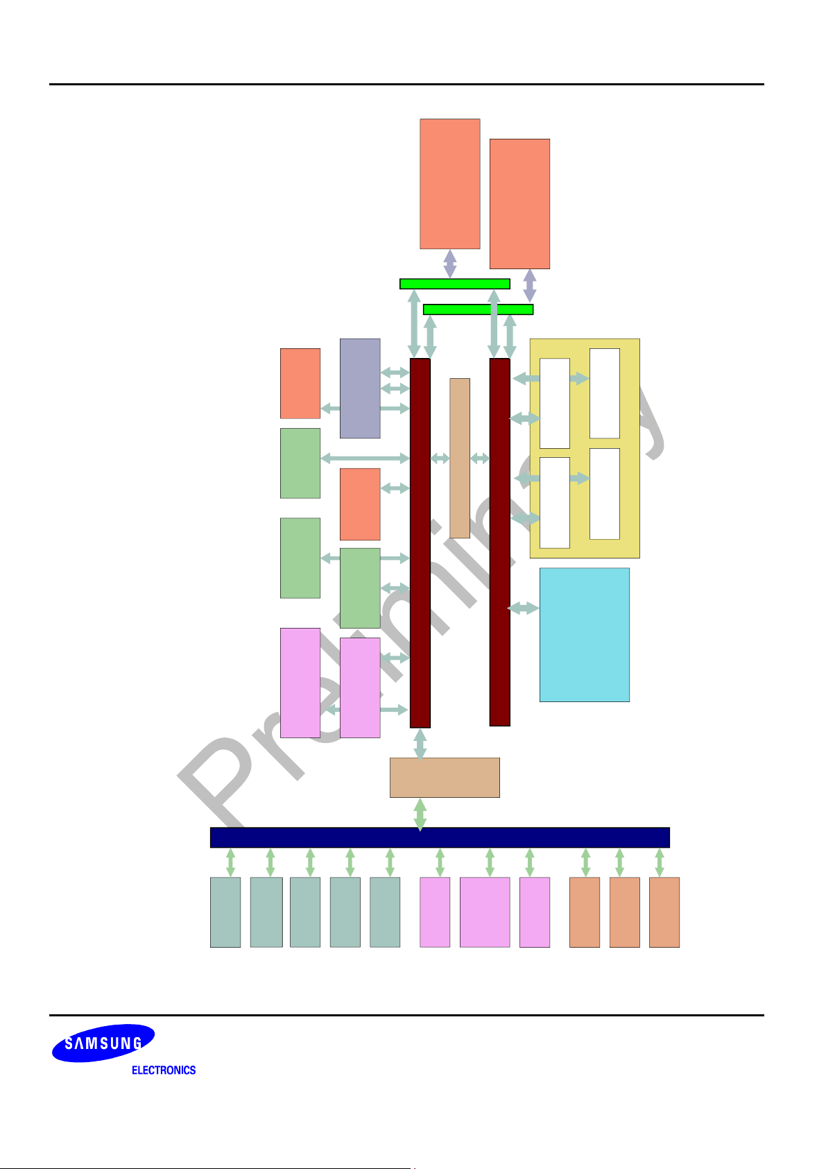
This section summarizes the features of the S3C24A0. Figure 1-1 is an overall block diagram of the S3C24A0.
1.2.1 Microprocessor and Overall Architecture
• SoC (System-on-Chip) for mobile phones and general embedded applications.
• 16/32-Bit RISC architecture and powerful instruction set with ARM926EJ- S CPU core.
• ARM’s Jazelle Java technology
• Enhanced ARM architecture MMU to support WinCE, Symbian and Linux
• Instruction cache, data cache, write buffer and Physical address TAG RAM to reduce the effect of main
memory bandwidth and latency on performance
Preliminary product information describes products that are in development,
for which full characterization data and associated errata are not yet available.
Specifications and information herein are subject to change without notice.
1-3
Page 4

BSW rv0.1-0417-N01
PRELIMINARY PRODUCT OVERVIEW S3C24A0 RISC MICROPROCESSOR
• 4 way set-associative cache with I-Cache (16KB) and D-Cache (16KB).
• 8-words per line with one valid bit and two dirty bits per line
• Pseudo random or round robin replacement algorithm.
• Write through or write back cache operation to update the main memory.
• The write buffer can hold 16 words of data and four addresses.
• ARM926EJ-S core supports the ARM debug architecture
• Internal AMBA (Advanced Microcontroller Bus Architecture) (AMBA2.0, AHB/APB)
• Dual AHB bus for high-performance processing (AHB-I & AHB-S)
1.2.2 Memory Subsystem
• High bandwidth Memory subsystem with two access channels (accesses from two AHB buses) and three-
channel memory ports
• Double the bandwidth with the simultaneous access capability
• ROM/SRAM/NOR-Flash/NAND-Flash channel
• One SDRAM channels
• Up to 1GB Address space
• Low-power SDRAM interface support : Mobile SDRAM function
- DS : Driver Strength Control
- TCSR : Temperature Compensated Self-Refresh Control
- PASR : Partial Array Self-Refresh Control
• NAND Flash Boot Loader with the ECC circuitry to support booting from NAND Flash
- 4KB Stepping Stone
- Support 1G, 2G bit NAND Flash
1.2.3 General Peripherals
• Interrupt Controller
- 61 Interrupt sources
(1 Watch D og Timer, 5 Timer, 6 UA RT, 18 External Interrupts, 4 DMA, 2 RTC, 3 ADC, 1 I2C, 1 AC97, 1
NAND Flash, 1 IrDA, 1 Memory Stick, 2 SPI, 1 SDI, 2 USB (Host and Device), 1 Keypad, 1 Modem
Interface, 2 Camera Interface, 4 MPEG, 2 LCD, 1 Battery Fault, 1 Post)
- Level/Edge mode on external interrupt source.
- Programmable polarity of edge and level.
- Supports FIQ (Fast Interrupt request) for very urgent interrupt request.
• Timer with PWM (Pulse Width Modulation)
- 4-ch 16-bit Timer with PWM / 1-ch 16-bit internal timer with DMA-based or interrupt-based operation
- Programmable duty cycle, frequency, and polarity
- Dead-zone generation.
- Support external clock source.
1-4
Preliminary product information describes products that are in development,
for which full characterization data and associated errata are not yet available.
Specifications and information herein are subject to change without notice.
Page 5

BSW rv0.1-0417-N01
S3C24A0 RISC MICROPROCESSOR PRELIMINARY PRODUCT OVERVIEW
• 16-bit Watchdog Timer.
- Interrupt request or system reset at time-out.
• 4-ch DMA controller.
- Support memory to memory, IO to memory, memory to IO, and IO to IO
- Burst transfer mode to enhance the transfer rate.
• RTC (Real Time Clock)
- Full clock feature: msec, sec, min, hour, day, date, week, month, year.
- 32.768 KHz operation
- Alarm interrupt
- Time-tick interrupt
1.2.4 Serial Communication
• UART
- 2-channel UART with DMA-based or interrupt-based operation
- Supports 5-bit, 6-bit, 7-bit, or 8-bit serial data transmit/receive
- Supports external clock for the UART operation (XuCLK)
- Programmable baud rate
- Supports IrDA 1.0
- Loop back mode for testing
- Each channel has internal 64- byte Tx FIFO and 64-byte Rx FIFO
• IrDA
- Support IrDA 1.1 (1.152Mbps and 4Mbps)
- Support FIFO operation in the MIR and FIR mode
- Configurable FIFO Size (16-byte or 64-byte)
- Support Back-to-Back Transactions
- Support Software Selection Temic-IBM or HP Transceiver
- Support Little-endian access
• IIC-Bus Interface
- 1-ch Multi-Master IIC-Bus
- Serial, 8-bit oriented and bi-directional data transfers can be made at up to 100 Kbit/s in the standard
mode
• IIS-Bus Interface
- 1-ch IIS-bus for the audio-codec interface with DMA-based operation
- Serial, 8/16-bit per channel data transfers
- 128 Bytes (64-Byte + 64-Byte) FIFO for receive/transmit
- Supports IIS format and MSB-justified data format
Preliminary product information describes products that are in development,
for which full characterization data and associated errata are not yet available.
Specifications and information herein are subject to change without notice.
1-5
Page 6

BSW rv0.1-0417-N01
PRELIMINARY PRODUCT OVERVIEW S3C24A0 RISC MICROPROCESSOR
• SPI Interface
- 2-ch Serial Peripheral Interface Protocol version 2.11 com pa t ible
- 2x8 bits Shift register for receive/transmit.
- DMA-based or interrupt-based operation.
• AC97 Audio-CODEC Interface
- 48KHz 16-bit sampling
- 1-ch stereo PCM inputs / 1-ch stereo PCM outputs / 1-ch MIC input
• USB Host
- 2-port USB Host
- Complies with OHCI Rev. 1.0
- Compatible with the USB Specification version 1.1
• USB Device
- 1-port USB Device
- 5 End-points for USB Device
- Compatible with the USB Specification version 1.1
1.2.5 Parallel Communication
• Modem Chip Interface
- 8-bit Asynchronous SRAM interface-style interface
- On-chip 2KB dual-ported SRAM buffer
- Interrupt Request for Data Exchange
- Programmable Interrupt Port Address
• 32-bit GPIO
- Fully configurable 32-bit GPIO
1.2.6 Image and Video Processing
• Camera Inteface
- ITU601/ITU656 YCbCr 4:2:2 8/16-bit mode
- Image down scaling capability for variable applications
- Digital Zoom-In
- Image X, Y-flip, 180 rotation
- Input Image Window Cut
- Two master for dedicated DMA operation
- Programmable burst length for DMA operation
- Programmable polarity of video sync signals
- Wide horizontal line buffer (maximum 2048 pixel)
1-6
Preliminary product information describes products that are in development,
for which full characterization data and associated errata are not yet available.
Specifications and information herein are subject to change without notice.
Page 7

BSW rv0.1-0417-N01
S3C24A0 RISC MICROPROCESSOR PRELIMINARY PRODUCT OVERVIEW
- Up to 4M pixel resolution support for scaled image (image preview or motion video capturing) and 16M
pixel for unscaled image (JPEG)
- Format conversion from YCrCb 4:2:2 to 4:2:0 for codec, and to RGB 4:4:4 for preview
• Hardware Accelerated MPEG4 Video Encoding/Decoding
- A AHB Interface
- Realtime MPEG-4 Video Encoding & Decoding
- Up to Simple Profile at Level 3 (352x288 at 30fps)
- Supports H.263 Base Line
• MPEG-4 ME (Motion Estimation)
- Highly optimized hard-wired engine
- Unrestricted Mode and Advanced Prediction Mode (4MV)
- Use the advanced MRMCS algorithm
- Half-pel search
- Programmable Image size up to 2048x2048
- Padding for Macro-block basis
- Search Range : [-16, 15.5]
- Intra/Inter Mode Decision MC (Motion Compensation)
• MC (Motion Compensation)
- Highly optimized hard-wired engine
- Unrestricted Mode and Advanced Prediction Mode (4MV)
- Half-pel search
- Programmable Image size up to 2048x2048
- Dedicated DMA
- Macroblock-based Pading
- Search Range : [-64, 63.5]
• DCTQ
- DCT/IDCT/Q/IQ operations•AMBA AHB Interface
- Support MPEG-4 Simple Profile Level 3 / H.263 Base-Line•Support programmable image size up to
4096x4096
- Macroblock-based processing
- Rate Control by Qp Information
- Local DMA
- Support MPEG-4 Encoding / Decoding
- Support JPEG DCT / IDCT Operation
- Operation unit : 1MB(MacroBlock) ~ 1 Frame
Preliminary product information describes products that are in development,
for which full characterization data and associated errata are not yet available.
Specifications and information herein are subject to change without notice.
1-7
Page 8

BSW rv0.1-0417-N01
PRELIMINARY PRODUCT OVERVIEW S3C24A0 RISC MICROPROCESSOR
• VLX
- VLC/VLD operations
- AMBA AHB Interface
- Support MPEG4 Simple Profile Level 3/ H.263. Baseline
- Macro block-based processing
- Dedicated DMA
- Only DCTQ coefficient VLC/VLD operation
- Only DC prediction operation in VLC
• Post Processor
- Dedicate DMA with Offset Address
- 3 Channel Scaling Pipelines for Video/Graphis Signal
- Input Format : YCbCr4:2:0, YCbCr4:2:2, or RGB 16b/24b
- Output Format : RGB 16b/24b
- Programmable Image Size (Source up to 4096x4096, Destination up to 2048x2048)
- Programmable Scale Ratio (Up-scale: up to Max. Destination Size, Down-scale: ~>1/64 in X & Y)
- Format Conversion for Video Signal (YCbCr4:2:0 or YCbCr4:2:2)
- Color Space Conversion (YCbCr2RGB)
- Separate Processing Clock from AHB Interface Clock
1.2.7 Display Control
• TFT LCD Interface
- 18-bit Parallel or 6bit*3 Interface
- 1/2/4/8-bpp Palletized or 8/16/18-bpp Non-Palletized Color-TFF support
- Supports 640x480, 320x240, 176x192 and others
- Up to 16 Mbyte virtual screen size
- Supports Multiple Virtual Display Screen (Supports Hardware Horizontal/Vertical Scrolling)
- Programmable timing control for different display panels
- Dual Buffer
• OSD (On Screen Display)
- Realtime overlay plane multiplexing
- Programmable OSD window positioning
- Per-pixel alpha blending for 18-bpp OSD images
- Fixedalpha- valuefor 8-/16-/1 8-bpp OSDimage
- 256-level alpha blending
- 24-bit color key support
- Dual buffer
1-8
Preliminary product information describes products that are in development,
for which full characterization data and associated errata are not yet available.
Specifications and information herein are subject to change without notice.
Page 9

BSW rv0.1-0417-N01
S3C24A0 RISC MICROPROCESSOR PRELIMINARY PRODUCT OVERVIEW
1.2.8 Input Devices
• Keypad Interface
- Provides internal debouncing filter
- 5-input, 5-output pins for key scan in/out
• A/D Converter and Touch Screen Interface
- 8-ch multiplexed ADC
- Max. 500K samples/ sec and 10-bit resolution
1.2.9 Storage Devices
• SD Host
- Compatible with SD Memory Card Protocol version 1.0
- Compatible with SDIO Card Protocol version 1.0
- 64 Bytes FIFO for Tx/Rx
- DMA based or Interrupt based operation
- Compatible with Multimedia Card Protocol version 2.11
• Memory Stick Host
- Memory Stick version 1.3 compliant
1.2.10 System Management
• Little Endian format support
• System operating clock generation
- Two on-chip PLLs, MPLL & UPLL
- MPLL generates the system reference clock, 200MHz@1.2V
- UPLL generates clocks for the USB Host/Device, IrDA and Camera
• Power Management
- Clock-off control for individual components
- Various power-down modes are available such as IDLE, STOP and SLEEP
- Wake - up by one of external interrupts or by the RTC alarm interrupt, etc.
1.2.11 Electrical Characteristics
• Operating Conditions
- - Supply Voltage for Logic Core: 1.25V +/- 0.05V
- - External Memory Interface: 1.8V / 2.5V / 3.3V
- - External I/O Interface: 3.3V
• Operational Frequency
- - Max. 200MHz@1.25V
Preliminary product information describes products that are in development,
for which full characterization data and associated errata are not yet available.
Specifications and information herein are subject to change without notice.
1-9
Page 10

BSW rv0.1-0417-N01
PRELIMINARY PRODUCT OVERVIEW S3C24A0 RISC MICROPROCESSOR
1.2.12 Package
• 337-pin FBGA (0.5mm pitch, 13mm x 13mm)
1-10
Preliminary product information describes products that are in development,
for which full characterization data and associated errata are not yet available.
Specifications and information herein are subject to change without notice.
Page 11
BSW rv0.1-0417-N01
S3C24A0 RISC MICROPROCESSOR PRELIMINARY PRODUCT OVERVIEW
SRAM/NOR/NAND
Memory Controller
Memory Controller
/ROM
SDRAM
IrDA1.1
Interface
Modem
4-Channel
DMA
Down Controller
System/Power
ARM926EJ
Inst. Data
USB 1.1
Host
INTC
NAND Boot
Loader
MPEG4 H/W Accelerator
Interface
ME/MC
Camera
AHB to AHB Bridge
Postprocessor
AHB-S
AHB-I
DCTQ/VLX
TFT LCD Interface
Digital Display
Controller
AHB to
APB Bridge
A
B
P
PI
I2C/I2S/S
UART*2
SD Host
Host
Memory
Stick
Device
USB1.1
Codec IF
Audio
Timer
KEYPAD
GPIO*32
ADC/
10-bit
Screen
Touch
Figure 1- 1 An Overall Block Diagram of the S3C24A0
Preliminary product information describes products that are in development,
for which full characterization data and associated errata are not yet available.
Specifications and information herein are subject to change without notice.
TIMER*5
Watch Dog
1-11
Page 12
BSW rv0.1-0417-N01
PRELIMINARY PRODUCT OVERVIEW S3C24A0 RISC MICROPROCESSOR
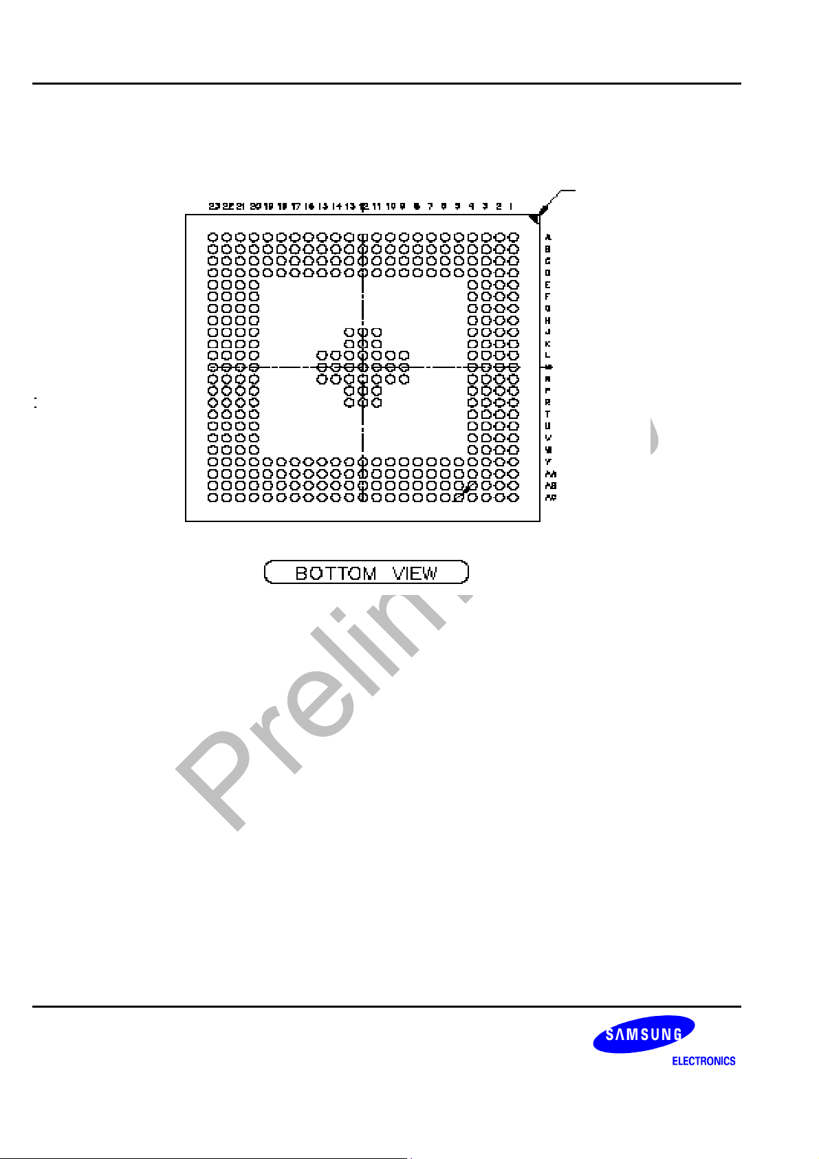
1.3.2 Pin Assignment
#A1 INDEX MARK
337-Pin FBGA Pin Assignment
1-12
Preliminary product information describes products that are in development,
for which full characterization data and associated errata are not yet available.
Specifications and information herein are subject to change without notice.
Page 13

BSW rv0.1-0417-N01
S3C24A0 RISC MICROPROCESSOR PRELIMINARY PRODUCT OVERVIEW
Table 1-1. 337-Pin FBGA Pin Assignments – Pin Number Order
Pin
Number
Pin Name
Pin
Number
Pin Name
Pin
Number
Pin Name
A01 XCIYDATA[4] B11 XRDATA[1] C21 XRADDR [21]
A02 VSS_B B12 XRDATA[3] C22 XFNFPS
A03 XCICDATA[0] B13 XRDATA[7] C23 XFNFADV
A04 XCIYDATA[7] B14 XRADDR[5] D01 XJTDO
A05 XCIPCLK B15 XRNWBE[0] D02 XJTDI
A06 XVVD[5] B16 XRWEN D03 XVVD[2]
A07 XVVD[7] B17 XRCSN[2] D04 XCIRSTN
A08 XVVCLK B18 XRDATA[14] D05 XCIYDATA[5]
A09 XVDEN B19 XRADDR[11] D06 XCIVSYNC
A10 XCICDATA[7] B20 XRADDR[15] D07 XVVD[13]
A11 XRDATA[0] B21 XRADDR[22] D08 XVVD[14]
A12 XRDATA[5] B22 XFALE D09 XCICDATA[5]
A13 XRADDR [3] B23 XFNFACYC D10 XJRTCK
A14 XRADDR [7] C01 XJTMS D11 XVVSYNC
A15 XRNWBE[1] C02 XJTRSTN D12 XVVD[19]
A16 XRDATA[8] C03 XCICLK D13 XVVD[22]
A17 XRDATA[13] C04 XCICDATA[1] D14 XRADDR [4]
A18 XRADDR [10] C05 XVVD[4] D15 XRADDR [2]
A19 XRADDR [16] C06 XCIHREF D16 XRADDR [0]
A20 XRADDR [17] C07 XCICDATA[4] D17 XRADDR [14]
A21 XRADDR[20] C08 XCICDATA[6] D18 XRADDR [19]
A22 XRADDR [23] C09 XVHSYNC D19 XFCLE
A23 XFRNB[0] C10 XVVD[20] D20 XRADDR [8]
B01 XJTCK C11 XVVD[23] D21 XRADDR [12]
B02 XCIYDATA[0] C12 VDD_C D22 XFNFBW
B03 XCIYDATA[2] C13 XRDATA[6] D23 XRADDR [25]
B04 XCIYDATA[6] C14 XRADDR[1] E01 XGPIO[31]
B05 XCICDATA[2] C15 XRADDR [6] E02 X2CSDA
B06 XCICDATA[3] C16 XRWAITN E03 X2CSCL
B07 XVVD[11] C17 XRCSN[1] E04 XCIYDATA[1]
B08 XVVD[15] C18 XRDATA[10] E20 XFRNB[1]
B09 XVVD[18] C19 XRDATA[12] E21 XRADDR [24]
B10 XVVD[21] C20 XRADDR [9] E22 XPDATA[2]
Preliminary product information describes products that are in development,
for which full characterization data and associated errata are not yet available.
Specifications and information herein are subject to change without notice.
1-13
Page 14

BSW rv0.1-0417-N01
PRELIMINARY PRODUCT OVERVIEW S3C24A0 RISC MICROPROCESSOR
Table 1-1. 337-Pin FBGA Pin Assignments – Pin Number Order
Pin
Number
Pin Name
Pin
Number
Pin Name
Pin
Number
Pin Name
E23 XPDATA[1] J21 VDD_A M09 VSS_B
F01 XGPIO[28] J22 XPDQM[3] M10 VDD_F
F02 XGPIO[29] J23 XPDATA[8] M11 VSS
F03 XGPIO[30] K01 XGPIO[11] M12 VSS
F04 XCIYDATA[3] K02 XGPIO[14] M13 VSS
F20 XRADDR [18] K03 XGPIO[16] M14 VDD_A
F21 XPDATA[0] K04 XVVD[12] M15 VSS_D
F22 XPDATA[6] K11 VDD_B M20 XPADDR[2]
F23 XPDATA[3] K12 VSS M21 XPDATA[15]
G01 XGPIO[24] K13 VSS_E M22 XPADDR[1]
G02 XGPIO[26] K20 XRDATA[11] M23 XPADDR[3]
G03 XGPIO[27] K21 XPDATA[9] N01 X97SYNC
G04 XVVD[3] K22 XPDATA[10] N02 X97RESETN
G20 XRADDR [13] K23 XPDATA[11] N03 XGPIO[4]
G21 XPDATA[5] L01 XGPIO[7] N04 XGPIO[8]
G22 XPDQM[0] L02 XGPIO[10] N09 VDD_A
G23 XPDATA[7] L03 XGPIO[12] N10 VDD_B
H01 XGPIO[20] L04 XGPIO[21] N11 VSS
H02 XGPIO[23] L09 VDD_C N12 VSS
H03 XGPIO[22] L10 VDD_C N13 VSS
H04 XVVD[6] L11 VSS N14 VSS_D
H20 XPDATA[4] L12 VSS N15 VDD_D
H21 VDD_D L13 VSS N20 XRDATA[9]
H22 XPDQM[1] L14 VDD_E N21 XPADDR[4]
H23 XPDQM[2] L15 VSS_D N22 XPADDR[5]
J01 XGPIO[17] L20 XPDATA[14] N23 XPADDR[6]
J02 XGPIO[18] L21 XPDATA[12] P01 XURTSN
J03 XGPIO[25] L22 XPDATA[13] P02 X97SDO
J04 XVVD[10] L23 XPADDR[0] P03 X97BITCLK
J11 VSS_B M01 XGPIO[0] P04 XGPIO[5]
J12 VSS_E M02 XGPIO[6] P11 VSS_B
J13 VDD_E M03 VDD_B P12 VDD_F
J20 XRDATA[15] M04 XGPIO[19] P13 VSS_D
1-14
Preliminary product information describes products that are in development,
for which full characterization data and associated errata are not yet available.
Specifications and information herein are subject to change without notice.
Page 15

BSW rv0.1-0417-N01
S3C24A0 RISC MICROPROCESSOR PRELIMINARY PRODUCT OVERVIEW
Table 1-1. 337-Pin FBGA Pin Assignments – Pin Number Order
Pin
Number
Pin Name
Pin
Number
Pin Name
Pin
Number
Pin Name
P20 XRCSN[0] V03 XGTMODE[3] Y20 VDD_D
P21 XPDATA[16] V04 XUCLK Y21 XPDATA[25]
P22 XPADDR[7] V20 XRDATA[2] Y22 XPDATA[27]
P23 XPDATA[18] V21 XPDATA[29] Y23 XPDATA[26]
R01 XGTMODE[2] V22 XPWEN AA01 XRTCXTI
R02 XURXD V23 XPCASN AA02 XGREFCLKSEL[0]
R03 XGPIO[2] W01 XGTMODE[1] AA03 XGPWROFFN
R04 XGPIO[15] W02 XSPIMISO AA04 XADCAIN[5]
R11 VDD_A W03 XSPISSIN[0] AA05 XADCAVREF
R12 VDD_B W04 X2SCLK AA06 XADCAIN[2]
R13 VSS_D W20 VDD_D AA07 GND10
R20 XROEN W21 VDD_A AA08 VDD13
R21 XPDATA[17] W22 XPCSN[0] AA09 XSRESETN
R22 XPDATA[19] W23 XPCSN[1] AA10 XSXTOUT
R23 XPSCLK Y01 XSWRESETN AA11 XUSDP[0]
T01 X2SCDCLK Y02 XGTMODE[0] AA12 XUSDN[0]
T02 XUCTSN Y03 XSPICLK AA13 XMSBS
T03 X97SDI Y04 X2SDI AA14 XMIWEN
T04 XGPIO[13] Y05 XGBATFLTN AA15 XMIADR[8]
T20 XPDATA[24] Y06 XGPIO[1] AA16 XMIADR[6]
T21 XPDATA[20] Y07 XGPIO[3] AA17 XMIDATA[6]
T22 XPDATA[21] Y08 VDD15 AA18 VDD_A
T23 XPDATA[23] Y09 XSRSTOUTN AA19 XMIDATA[2]
U01 X2SDO Y10 XUDDP AA20 XMIADR[0]
U02 X2SLRCK Y11 XSDDAT[3] AA21 VDD_D
U03 XUTXD Y12 VDD20(VDDpadUSB) AA22 XPDATA[31]
U04 XGPIO[9] Y13 XMSSDIO AA23 XPDATA[28]
U20 XRDATA[4] Y14 XMSPI AB01 VDD10
U21 XPDATA[22] Y15 XMICSN AB02 XADCAIN[7]
U22 XPCKE Y16 XMIADR[10] AB03 XRTCXTO
U23 XPRASN Y17 XPADDR[13] AB04 XGREFCLKSEL[1]
V01 XSPIMOSI Y18 XMIADR[4] AB05 XADCAIN[0]
V02 XSPISSIN[1] Y19 XMIADR[2] AB06 VDD11
Preliminary product information describes products that are in development,
for which full characterization data and associated errata are not yet available.
Specifications and information herein are subject to change without notice.
1-15
Page 16

BSW rv0.1-0417-N01
PRELIMINARY PRODUCT OVERVIEW S3C24A0 RISC MICROPROCESSOR
Table 1-1. 337-Pin FBGA Pin Assignments – Pin Number Order
Pin
Number
Pin Name
Pin
Number
Pin Name
Pin
Number
Pin Name
AB07 GND12 AB21 XPADDR[11] AC12 XSDDAT[2]
AB08 XSUPLLCAP AB22 XPDATA[30] AC13 XSDDAT[0]
AB09 XSEXTCLK AB23 XPADDR[8] AC14 XMIADR[9]
AB10 XUSDP[1] AC01 GND9(VSSrtc) AC15 XMIADR[5]
AB11 XUDDN AC02 XADCAIN[6] AC16 XMIDATA[5]
AB12 XSDDAT[1] AC03 XADCAIN[4] AC17 XMIDATA[3]
AB13 GND19(VSSpadUSB) AC04 XADCAIN[3] AC18 XMIDATA[1]
AB14 XMIOEN AC05 XADCAIN[1] AC19 XMIADR[3]
AB15 XMIADR[7] AC06 XSMPLLCAP AC20 XPADDR[14]
AB16 XMIDATA[7] AC07 GND14 AC21 XPADDR[12]
AB17 XMIDATA[4] AC08 XGMONHCLK AC22 XPADDR[10]
AB18 XMIIRQN AC09 XSXTIN AC23 XPADDR[9]
AB19 XMIDATA[0] AC10 XUSDN[1]
AB20 XMIADR[1] AC11 XMSSCLKO
1-16
Preliminary product information describes products that are in development,
for which full characterization data and associated errata are not yet available.
Specifications and information herein are subject to change without notice.
Page 17

BSW rv0.1-0417-N01
S3C24A0 RISC MICROPROCESSOR PRELIMINARY PRODUCT OVERVIEW
Table 1-2. 337-Pin FBGA Pin Assignments
Pin
Number
AA7 VSSadc VSSadc
AB7 VSSMpll VSSMpll
AC7 VSSUpll VSSUpll
AB13 VSSpadUSB VSSpadUSB
AC1 VSSrtc VSSrtc
AA18 VDDlogic VDDlogic
J21 VDDlogic VDDlogic
M14 VDDlogic VDDlogic
N9 VDDlogic VDDlogic
R11 VDDlogic VDDlogic
W21 VDDlogic VDDlogic
K11 VDDpadIO VDDpadIO
M3 VDDpadIO VDDpadIO
N10 VDDpadIO VDDpadIO
R12 VDDpadIO VDDpadIO
C12 VDDarm VDDarm
L10 VDDarm VDDarm
L9 VDDarm VDDarm
AA21 VDDpadSDRAM VDDpadSDRAM
H21 VDDpadSDRAM VDDpadSDRAM
N14 VSS VSS
N15 VDDpadSDRAM VDDpadSDRAM
W20 VDDpadSDRAM VDDpadSDRAM
Y20 VDDpadSDRAM VDDpadSDRAM
J13 VDDpadFlash VDDpadFlash
L14 VDDpadFlash VDDpadFlash
M10 VDDalive VDDalive
P12 VDDalive VDDalive
AB1 VDDrtc VDDrtc
AB6 VDDadc VDDadc
AA8 VDDMpll VDDMpll
Y8 VDDupll VDDupll
Y12 VDDpadUSB VDDpadUSB
K12 VSS VSS
L11 VSS VSS
L12 VSS VSS
L13 VSS VSS
Name Default Function I/O
I/O state@ Reset mode
(Data/En/PullupEn)
En(L)=>output
PullupEn(L)=>PullUp
P
P
P
P
P
P
P
P
P
P
P
P
P
P
P
P
P
P
P
P
P
P
P
P
P
P
P
P
P
P
P
P
P
P
P
P
P
I/O
State@SLEEP
mode
P
P
P
P
P
P
P
P
P
P
P
P
P
P
P
P
P
P
P
P
P
P
P
P
P
P
P
P
P
P
P
P
P
P
P
P
P
PP P
PP P
PP P
PP P
PP P
PP P
PP P
PP P
PP P
PP P
PP P
PP P
PP P
PP P
PP P
PP P
PP P
PP P
PP P
PP P
PP P
PP P
PP P
PP P
PP P
PP P
PP P
PP P
PP P
PP P
PP P
PP P
PP P
PP P
PP P
PP P
PP P
I/O
State@STOP
mode
Cell Type
(24A0A)
Preliminary product information describes products that are in development,
for which full characterization data and associated errata are not yet available.
Specifications and information herein are subject to change without notice.
1-17
Page 18

BSW rv0.1-0417-N01
PRELIMINARY PRODUCT OVERVIEW S3C24A0 RISC MICROPROCESSOR
Table 1-2. 337-Pin FBGA Pin Assignments
Pin
Number
M11 VSS VSS
M12 VSS VSS
M13 VSS VSS
N11 VSS VSS
N12 VSS VSS
N13 VSS VSS
A2 VSSpadIO VSSpadIO
J11 VSSpadIO VSSpadIO
M9 VSSpadIO VSSpadIO
P11 VSSpadIO VSSpadIO
L15 VSSpadSDRAM VSSpadSDRAM
M15 VSSpadSDRAM VSSpadSDRAM
P13 VSSpadSDRAM VSSpadSDRAM
R13 VSSpadSDRAM VSSpadSDRAM
J12 VSSpadFlash VSSpadFlash
K13 VSSpadFlash VSSpadFlash
E3
E2
Name
X2cSCL X2cSCL I/O I/H L or I H phbsud8sm
X2cSDA X2cSDA I/O I/H L or I H phbsud8sm
Default
Function
I/O state@ Reset mode
I/O
(Data/En/PullupEn)
En(L)=>output
PullupEn(L)=>PullUp
P
P
P
P
P
P
P
P
P
P
P
P
P
P
P
P
I/O
State@SLEEP
mode
P
P
P
P
P
P
P
P
P
P
P
P
P
P
P
P
PP P
PP P
PP P
PP P
PP P
PP P
PP P
PP P
PP P
PP P
PP P
PP P
PP P
PP P
PP P
PP P
I/O
State@STOP
mode
Cell Type
(24A0A)
T1
W4
Y4
U1
U2
P3
N2
T3
P2
N1
AB5
AC5
AA6
X2sCDCLK X2sCDCLK O H or L/L Hi-z or H or L H phot8
X2sCLK X2sCLK I/O L/L/L H or L or I L phbsu100ct8sm
X2sDI X2sDI I I - - phisu
X2sDO X2sDO O L/L Hi-z or H or L L phot8
X2sLRCK X2sLRCK I/O H/L/L H or L or I Pre phbsu100ct8sm
X97BITCLK X97BITCLK I I - - phis
X97RESETn X97RESETn O L/L Hi-z or H or L H phot8
X97SDI X97SDI I I - - phisu
X97SDO X97SDO O L/L Hi-z or H or L L phot8
X97SYNC X97SYNC O L/L Hi-z or H or L L phot8
XadcAIN[0] XadcAIN[0] Ain I - - phiar10_abb
XadcAIN[1] XadcAIN[1] Ain I - - phiar10_abb
XadcAIN[2] XadcAIN[2] Ain I - - phiar10_abb
1-18
Preliminary product information describes products that are in development,
for which full characterization data and associated errata are not yet available.
Specifications and information herein are subject to change without notice.
Page 19

BSW rv0.1-0417-N01
S3C24A0 RISC MICROPROCESSOR PRELIMINARY PRODUCT OVERVIEW
Table 1-2. 337-Pin FBGA Pin Assignments
Pin
Number
AC4
AC3
AA4
AC2
AB2
AA5
A3
C4
B5
B6
C7
D9
C8
A10
I/O state@ Reset mode
Name
XadcAIN[3] XadcAIN[3] Ain I - - phiar10_abb
XadcAIN[4] XadcAIN[4] Ain I - - phiar10_abb
XadcAIN[5] XadcAIN[5] Ain I - - phiar10_abb
XadcAIN[6] XadcAIN[6] Ain I - - phiar10_abb
XadcAIN[7] XadcAIN[7] Ain I - - phiar10_abb
XadcAVREF XadcAVREF Ain I - - phia_abb
XciCDATA[0] XciCDATA[0] I I/H/L - - phbsu100ct8sm
XciCDATA[1] XciCDATA[1] I I/H/L - - phb su100ct8sm
XciCDATA[2] XciCDATA[2] I I/H/L - - phb su100ct8sm
XciCDATA[3] XciCDATA[3] I I/H/L - - phb su100ct8sm
XciCDATA[4] XciCDATA[4] I I/H/L - - phb su100ct8sm
XciCDATA[5] XciCDATA[5] I I/H/L - - phbsu100ct8sm
XciCDATA[6] XciCDATA[6] I I/H/L - - phb su100ct8sm
XciCDATA[7] XciCDATA[7] I I/H/L - - phb su100ct8sm
Default
Function
I/O
(Data/En/PullupEn)
En(L)=>output
PullupEn(L)=>PullUp
I/O
State@SLEEP
mode
I/O
State@STOP
mode
Cell Type
(24A0A)
C3
C6
A5
D4
D6
B2
E4
B3
F4
A1
D5
B4
A4
B22
D19
XciCLK XciCLK O L/L Hi-z or H or L L phot12sm
XciHREF XciHREF I I - - phis
XciPCLK XciPCLK I I - - phis
XciRSTn XciRSTn O L/L Hi-z or H or L Pre phot8
XciVSYNC XciVSYNC I I - - phis
XciYDATA[0] XciYDATA[0] I I - - phis
XciYDATA[1] XciYDATA[1] I I - - phis
XciYDATA[2] XciYDATA[2] I I - - phis
XciYDATA[3] XciYDATA[3] I I - - phis
XciYDATA[4] XciYDATA[4] I I - - phis
XciYDATA[5] XciYDATA[5] I I - - phis
XciYDATA[6] XciYDATA[6] I I - - phis
XciYDATA[7] XciYDATA[7] I I - - phis
XfALE XfALE O L/L Hi-z or H or L L phot8
XfCLE XfCLE O L/L Hi-z or H or L L phot8
Preliminary product information describes products that are in development,
for which full characterization data and associated errata are not yet available.
Specifications and information herein are subject to change without notice.
1-19
Page 20

BSW rv0.1-0417-N01
r
PRELIMINARY PRODUCT OVERVIEW S3C24A0 RISC MICROPROCESSOR
Table 1-2. 337-Pin FBGA Pin Assignments
I/O state@ Reset
Pin
Numbe
B23
C23
D22
C22
A23
E20
Y5
mode
Name
XfNFACYC XfNFACYC I I - - phis
XfNFADV XfNFADV I I - - phis
XfNFBW XfNFBW I I - - phis
XfNFPS XfNFPS I I - - phis
XfRnB[0] XfRnB[0] I I - - phisu
XfRnB[1] XfRnB[1] I I - - phisu
XgBATFLT XgBATFLT I H - - phis
Default
Function
(Data/En/PullupEn)
I/O
En(L)=>output
PullupEn(L)=>PullU
p
I/O
State@SLEEP
mode
I/O
State@STOP
mode
Cell Type
(24A0A)
AC8
M1
Y6
L2
K1
L3
T4
XgpIO[14]/EINT14/RTC_ALMINT XgpIO[14] I/O I/H/L H or L or I -
K2
XgpIO[15]/EINT15/XspiMOSI XgpIO[15] I/O I/H/L H or L or I -
R4
XgpIO[16]/EINT16/XspiMISO XgpIO[16] I/O I/H/L H or L or I -
K3
J1
XgpIO[18]/EINT18/XkpROW0 XgpIO[18] I/O I/H/L H or L or I -
J2
XgpIO[19]/PWM_ECLK/XkpROW
M4
XgpIO[2]/EINT2/PWM_TOUT0 XgpIO[2] I/O I/H/L H or L or I -
R3
H1
L4
XgMONHCLK XgMONHCLK O L/L Hi-z or H or L L phot8
XgpIO[0]/EINT0 XgpIO[0] I/O I/H/L H or L or I -
XgpIO[1]/EINT1 XgpIO[1] I/O I/H/L H or L or I -
XgpIO[10]/YMON XgpIO[10] I/O I/H/L H or L or I -
XgpIO[11]/EINT11 XgpIO[11] I/O I/H/L H or L or I -
XgpIO[12]/EINT12/XMON XgpIO[12] I/O I/H/L H or L or I -
XgpIO[13]/EINT13/XPON XgpIO[13] I/O I/H/L H or L or I -
XgpIO[17]/EINT17/XspiCLK XgpIO[17] I/O I/H/L H or L or I -
1
XgpIO[20]/PWM_TOUT0/
XkpROW2
XgpIO[21]/PWM_TOUT1/
XkpROW3
XgpIO[19] I/O I/H/L H or L or I -
XgpIO[20] I/O I/H/L H or L or I -
XgpIO[21] I/O I/H/L H or L or I -
phbsu100ct8s
m
phbsu100ct8s
m
phbsu100ct8s
m
phbsu100ct8s
m
phbsu100ct8s
m
phbsu100ct8s
m
phbsu100ct8s
m
phbsu100ct8s
m
phbsu100ct8s
m
phbsu100ct8s
m
phbsu100ct8s
m
phbsu100ct8s
m
phbsu100ct8s
m
phbsu100ct8s
m
phbsu100ct8s
m
1-20
Preliminary product information describes products that are in development,
for which full characterization data and associated errata are not yet available.
Specifications and information herein are subject to change without notice.
Page 21

BSW rv0.1-0417-N01
r
s
s
s
s
s
s
s
s
s
s
s
s
s
s
s
s
s
S3C24A0 RISC MICROPROCESSOR PRELIMINARY PRODUCT OVERVIEW
Table 1-2. 337-Pin FBGA Pin Assignments
I/O state@ Reset
Pin
Numbe
H3
H2
G1
J3
G2
G3
F1
F2
Y7
F3
E1
N3
P4
M2
L1
N4
U4
AA3
AA2
AB4
mode
Name Default Function I/O
XgpIO[22]/PWM_TOUT2/XkpROW4 XgpIO[22] I/O I/H/L H or L or I -
XgpIO[23]/PWM_TOUT3/XkpCOL0 XgpIO[23] I/O I/H/L H or L or I -
XgpIO[24]/EXTDMA_REQ0/
XkpCOL1
XgpIO[25]/EXTDMA_REQ1/
XkpCOL2
XgpIO[26]/EXTDMA_ACK0/
XkpCOL3
XgpIO[27]/EXTDMA_ACK1/XkpCOL4 XgpIO[27] I/O I/H/L H or L or I -
XgpIO[28]/XuCTSn1/RTC_ALMINT XgpIO[28] I/O I/H/L H or L or I -
XgpIO[29]/XuRTSn1/IrDA_SDBW XgpIO[29] I/O I/H/L H or L or I -
XgpIO[3]/EINT3/PWM_TOUT1 XgpIO[3] I/O I/H/L H or L or I -
XgpIO[30]/XuTXD1/IrDA_TXD XgpIO[30] I/O I/H/L H or L or I -
XgpIO[31]/XuRXD1/ IrDA_RXD XgpIO[31] I/O I/H/L H or L or I -
XgpIO[4]/EINT4/PWM_TOUT2 XgpIO[4] I/O I/H/L H or L or I -
XgpIO[5]/EINT5/ PWM_TOUT3 XgpIO[5] I/O I/H/L H or L or I -
XgpIO[6]/EINT6/EXTDMA_REQ0 XgpIO[6] I/O I/H/L H or L or I -
XgpIO[7]/EINT7 EXTDMA_REQ1 XgpIO[7] I/O I/H/L H or L or I -
XgpIO[8]/EINT8/ EXTDMA_ACK0 XgpIO[8] I/O I/H/L H or L or I -
XgpIO[9]/EINT9 EXTDMA_ACK1 XgpIO[9] I/O I/H/L H or L or I -
XgPWROFFn XgPWROFFn O H L H phob8
XgREFCLKSEL[0] XgREFCLKSEL[0] I H - - phis
XgREFCLKSEL[1] XgREFCLKSEL[1] I H - - phis
XgpIO[24] I/O I/H/L H or L or I -
XgpIO[25] I/O I/H/L H or L or I -
XgpIO[26] I/O I/H/L H or L or I -
(Data/En/PullupEn)
En(L)=>output
PullupEn(L)=>PullU
p
I/O
State@SLEEP
mode
I/O
State@STOP
mode
Cell Type
phbsu100ct8
phbsu100ct8
phbsu100ct8
phbsu100ct8
phbsu100ct8
phbsu100ct8
phbsu100ct8
phbsu100ct8
phbsu100ct8
phbsu100ct8
phbsu100ct8
phbsu100ct8
phbsu100ct8
phbsu100ct8
phbsu100ct8
phbsu100ct8
phbsu100ct8
(24A0A)
m
m
m
m
m
m
m
m
m
m
m
m
m
m
m
m
m
1-21
Preliminary product information describes products that are in development,
for which full characterization data and associated errata are not yet available.
Specifications and information herein are subject to change without notice.
Page 22

BSW rv0.1-0417-N01
PRELIMINARY PRODUCT OVERVIEW S3C24A0 RISC MICROPROCESSOR
Table 1-2. 337-Pin FBGA Pin Assignments
Pin
Number
Y2
W1
R1
V3
D10
B1
D2
D1
C1
C2
AA20
AB20
Y16
Y19
AC19
Y18
AC15
AA16
AB15
AA15
AC14
Y15
I/O state@ Reset mode
Name
XgTMODE[0] XgTMODE[0] I I - - phis
XgTMODE[1] XgTMODE[1] I I - - phis
XgTMODE[2] XgTMODE[2] I I - - phis
XgTMODE[3] XgTMODE[3] I I - - phis
XjRTCK XjRTCK O L - - phob8
XjTCK XjTCK I I - - phis
XjTDI XjTDI I I - - phisu
XjTDO XjTDO O I/H Hi-z or H or L Hi-z phot8
XjTMS XjTMS I I - - phisu
XjTRSTn XjTRSTn I I - - phisu
XmiADR[0] XmiADR[0] I I/H/L - - phbsu100ct8sm
XmiADR[1] XmiADR[1] I I/H/L - - phbsu100ct8sm
XmiADR[10] XmiADR[10] I I/H/L - - phbsu100ct8sm
XmiADR[2] XmiADR[2] I I/H/L - - phbsu100ct8sm
XmiADR[3] XmiADR[3] I I/H/L - - phbsu100ct8sm
XmiADR[4] XmiADR[4] I I/H/L - - phbsu100ct8sm
XmiADR[5] XmiADR[5] I I/H/L - - phbsu100ct8sm
XmiADR[6] XmiADR[6] I I/H/L - - phbsu100ct8sm
XmiADR[7] XmiADR[7] I I/H/L - - phbsu100ct8sm
XmiADR[8] XmiADR[8] I I/H/L - - phbsu100ct8sm
XmiADR[9] XmiADR[9] I I/H/L - - phbsu100ct8sm
XmiCSn XmiCSn I I - - phisu
Default
Function
I/O
(Data/En/PullupEn)
En(L)=>output
PullupEn(L)=>PullUp
I/O
State@SLEEP
mode
I/O
State@STOP
mode
Cell Type
(24A0A)
AB19
AC18
AA19
AC17
AB17
AC16
AA17
AB16
1-22
XmiDATA[0] XmiDATA[0] I/O I/H/L H or L or I - phbsu100ct8sm
XmiDATA[1] XmiDATA[1] I/O I/H/L H or L or I - phbsu100ct8sm
XmiDATA[2] XmiDATA[2] I/O I/H/L H or L or I - phbsu100ct8sm
XmiDATA[3] XmiDATA[3] I/O I/H/L H or L or I - phbsu100ct8sm
XmiDATA[4] XmiDATA[4] I/O I/H/L H or L or I - phbsu100ct8sm
XmiDATA[5] XmiDATA[5] I/O I/H/L H or L or I - phbsu100ct8sm
XmiDATA[6] XmiDATA[6] I/O I/H/L H or L or I - phbsu100ct8sm
XmiDATA[7] XmiDATA[7] I/O I/H/L H or L or I - phbsu100ct8sm
Preliminary product information describes products that are in development,
for which full characterization data and associated errata are not yet available.
Specifications and information herein are subject to change without notice.
Page 23

BSW rv0.1-0417-N01
S3C24A0 RISC MICROPROCESSOR PRELIMINARY PRODUCT OVERVIEW
Table 1-2. 337-Pin FBGA Pin Assignments
Pin
Number
AB18
AB14
AA14
AA13
Y14
AC11
Y13
L23
M22
AC22
AB21
AC21
I/O state@ Reset mode
Name
XmiIRQn XmiIRQn O H/L Hi-z or H or L H phot8
XmiOEn XmiOEn I I - - phisu
XmiWEn XmiWEn I I - - phisu
XmsBS XmsBS O L/L Hi-z or H or L L phot8
XmsPI XmsPI I I - - phis
XmsSCLKO XmsSCLKO O H/L Hi-z or H or L H phot8
XmsSDIO XmsSDIO I/O I/H/L H or L or I -
XpADDR[0] XpADDR[0] O
XpADDR[1] XpADDR[1] O
XpADDR[10] XpADDR[10] O
XpADDR[11] XpADDR[11] O
XpADDR[12] XpADDR[12] O
Default
Function
I/O
(Data/En/PullupEn)
En(L)=>output
PullupEn(L)=>PullUp
L/L
L/L
L/L
L/L
L/L
I/O
State@SLEEP
mode
Hi-z or H or L Pre phot12sm
Hi-z or H or L Pre phot12sm
Hi-z or H or L Pre phot12sm
Hi-z or H or L Pre phot12sm
Hi-z or H or L Pre phot12sm
I/O
State@STOP
mode
Cell Type
(24A0A)
phbsu100ct12s
m
Y17
AC20
M20
M23
N21
N22
N23
P22
AB23
AC23
V23
U22
XpADDR[13] XpADDR[13] O
XpADDR[14] XpADDR[14] O
XpADDR[2] XpADDR[2] O
XpADDR[3] XpADDR[3] O
XpADDR[4] XpADDR[4] O
XpADDR[5] XpADDR[5] O
XpADDR[6] XpADDR[6] O
XpADDR[7] XpADDR[7] O
XpADDR[8] XpADDR[8] O
XpADDR[9] XpADDR[9] O
XpCASn XpCASn O H/L Hi-z or H or L Pre phot12sm
XpCKE XpCKE O L/L Hi-z or H or L L phot12sm
L/L
L/L
L/L
L/L
L/L
L/L
L/L
L/L
L/L
L/L
Hi-z or H or L Pre phot12sm
Hi-z or H or L Pre phot12sm
Hi-z or H or L Pre phot12sm
Hi-z or H or L Pre phot12sm
Hi-z or H or L Pre phot12sm
Hi-z or H or L Pre phot12sm
Hi-z or H or L Pre phot12sm
Hi-z or H or L Pre phot12sm
Hi-z or H or L Pre phot12sm
Hi-z or H or L Pre phot12sm
Preliminary product information describes products that are in development,
for which full characterization data and associated errata are not yet available.
Specifications and information herein are subject to change without notice.
1-23
Page 24

BSW rv0.1-0417-N01
PRELIMINARY PRODUCT OVERVIEW S3C24A0 RISC MICROPROCESSOR
Table 1-2. 337-Pin FBGA Pin Assignments
Pin
Number
W22
W23
F21
E23
K22
K23
L21
L22
L20
M21
P21
R21
P23
R22
E22
T21
T22
U21
T23
T20
Y21
Y23
Y22
I/O state@ Reset mode
Name
XpCSN[0] XpCSN[0] O H/L Hi-z or H or L H phot12sm
XpCSN[1] XpCSN[1] O H/L Hi-z or H or L H phot12sm
XpDATA[0] XpDATA[0] I/O I/H/L H or L or I -
XpDATA[1] XpDATA[1] I/O I/H/L H or L or I -
XpDATA[10] XpDATA[10] I/O I/H/L H or L or I -
XpDATA[11] XpDATA[11] I/O I/H/L H or L or I -
XpDATA[12] XpDATA[12] I/O I/H/L H or L or I -
XpDATA[13] XpDATA[13] I/O I/H/L H or L or I -
XpDATA[14] XpDATA[14] I/O I/H/L H or L or I -
XpDATA[15] XpDATA[15] I/O I/H/L H or L or I -
XpDATA[16] XpDATA[16] I/O I/H/L H or L or I -
XpDATA[17] XpDATA[17] I/O I/H/L H or L or I -
XpDATA[18] XpDATA[18] I/O I/H/L H or L or I -
XpDATA[19] XpDATA[19] I/O I/H/L H or L or I -
XpDATA[2] XpDATA[2] I/O I/H/L H or L or I -
XpDATA[20] XpDATA[20] I/O I/H/L H or L or I -
XpDATA[21] XpDATA[21] I/O I/H/L H or L or I -
XpDATA[22] XpDATA[22] I/O I/H/L H or L or I -
XpDATA[23] XpDATA[23] I/O I/H/L H or L or I -
XpDATA[24] XpDATA[24] I/O I/H/L H or L or I -
XpDATA[25] XpDATA[25] I/O I/H/L H or L or I -
XpDATA[26] XpDATA[26] I/O I/H/L H or L or I -
XpDATA[27] XpDATA[27] I/O I/H/ L H or L or I -
Default
Function
I/O
(Data/En/PullupEn)
En(L)=>output
PullupEn(L)=>PullUp
I/O
State@SLEEP
mode
I/O
State@STOP
mode
Cell Type
(24A0A)
phbsu100ct12s
m
phbsu100ct12s
m
phbsu100ct12s
m
phbsu100ct12s
m
phbsu100ct12s
m
phbsu100ct12s
m
phbsu100ct12s
m
phbsu100ct12s
m
phbsu100ct12s
m
phbsu100ct12s
m
phbsu100ct12s
m
phbsu100ct12s
m
phbsu100ct12s
m
phbsu100ct12s
m
phbsu100ct12s
m
phbsu100ct12s
m
phbsu100ct12s
m
phbsu100ct12s
m
phbsu100ct12s
m
phbsu100ct12s
m
phbsu100ct12s
m
1-24
Preliminary product information describes products that are in development,
for which full characterization data and associated errata are not yet available.
Specifications and information herein are subject to change without notice.
Page 25

BSW rv0.1-0417-N01
r
S3C24A0 RISC MICROPROCESSOR PRELIMINARY PRODUCT OVERVIEW
Table 1-2. 337-Pin FBGA Pin Assignments
Pin
Numbe
AA23
V21
F23
AB22
AA22
H20
G21
F22
G23
J23
K21
I/O state@ Reset mode
Name Default Function I/O
XpDATA[28] XpDATA[28] I/O I/H/L H or L or I XpDATA[29] XpDATA[29] I/O I/H/L H or L or I -
XpDATA[3] XpDATA[3] I/O I/H/L H or L or I -
XpDATA[30] XpDATA[30] I/O I/H/L H or L or I -
XpDATA[31] XpDATA[31] I/O I/H/L H or L or I -
XpDATA[4] XpDATA[4] I/O I/H/L H or L or I -
XpDATA[5] XpDATA[5] I/O I/H/L H or L or I -
XpDATA[6] XpDATA[6] I/O I/H/L H or L or I -
XpDATA[7] XpDATA[7] I/O I/H/L H or L or I -
XpDATA[8] XpDATA[8] I/O I/H/L H or L or I -
XpDATA[9] XpDATA[9] I/O I/H/L H or L or I -
(Data/En/PullupEn)
En(L)=>output
PullupEn(L)=>PullUp
I/O
State@SLEEP
mode
State@STOP
mode
I/O
Cell Type
(24A0A)
phbsu100ct12s
m
phbsu100ct12s
m
phbsu100ct12s
m
phbsu100ct12s
m
phbsu100ct12s
m
phbsu100ct12s
m
phbsu100ct12s
m
phbsu100ct12s
m
phbsu100ct12s
m
phbsu100ct12s
m
phbsu100ct12s
m
G22
H22
H23
J22
U23
R23
V22
D16
C14
A18
B19
D21
XpDQM[0] XpDQM[0] O
XpDQM[1] XpDQM[1] O
XpDQM[2] XpDQM[2] O
XpDQM[3] XpDQM[3] O
XpRASn XpRASn O
XpSCLK XpSCLK I/O
XpWEn XpWEn O
XrADDR[0] XrADDR[0] O L/L Hi-z or H or L Pre phot8
XrADDR[1] XrADDR[1] O L/L Hi-z or H or L Pre phot8
XrADDR[10] XrADDR[10] O L/L Hi-z or H or L Pre phot8
XrADDR[11] XrADDR[11] O L/L Hi-z or H or L Pre phot8
XrADDR[12] XrADDR[12] O L/L Hi-z or H or L Pre phot8
H/L
H/L
H/L
H/L
H/L
H or L /L
H/L
Hi-z or H or L - phot12sm
Hi-z or H or L - phot12sm
Hi-z or H or L - phot12sm
Hi-z or H or L - phot12sm
Hi-z or H or L - phot12sm
H or L or I L phbst12
Hi-z or H or L H phot12sm
1-25
Preliminary product information describes products that are in development,
for which full characterization data and associated errata are not yet available.
Specifications and information herein are subject to change without notice.
Page 26

BSW rv0.1-0417-N01
PRELIMINARY PRODUCT OVERVIEW S3C24A0 RISC MICROPROCESSOR
Table 1-2. 337-Pin FBGA Pin Assignments
I/O state@ Reset
Pin
Number
Name Default Function I/O
mode
(Data/En/PullupEn)
En(L)=>output
PullupEn(L)=>PullUp
I/O
State@SLEEP
mode
I/O
State@STOP
mode
Cell Type
(24A0A)
G20
D17
B20
A19
A20
D15
A13
D14
B14
C15
A14
D20
XrADDR[13] XrADDR[13] O L/L Hi-z or H or L Pre phot8
XrADDR[14] XrADDR[14] O L/L Hi-z or H or L Pre phot8
XrADDR[15] XrADDR[15] O L/L Hi-z or H or L Pre phot8
XrADDR[16] XrADDR[16] O L/L Hi-z or H or L Pre phot8
XrADDR[17] XrADDR[17] O L/L Hi-z or H or L Pre phot8
XrADDR[2] XrADDR[2] O L/L Hi-z or H or L Pre phot8
XrADDR[3] XrADDR[3] O L/L Hi-z or H or L Pre phot8
XrADDR[4] XrADDR[4] O L/L Hi-z or H or L Pre phot8
XrADDR[5] XrADDR[5] O L/L Hi-z or H or L Pre phot8
XrADDR[6] XrADDR[6] O L/L Hi-z or H or L Pre phot8
XrADDR[7] XrADDR[7] O L/L Hi-z or H or L Pre phot8
XrADDR[8] XrADDR[8] O L/L Hi-z or H or L Pre phot8
C20
F20
D18
A21
C21
B21
A22
E21
D23
P20
1-26
XrADDR [9] XrADDR [9] O L/L Hi-z or H or L Pre phot8
XrADDR[18] XrADDR[18] O L/L/H Hi-z or H or L Pre
XrADDR[19] XrADDR[19] O L/L/H Hi-z or H or L Pre phbsu100ct8sm
XrADDR[20] XrADDR[20] O L/L/H Hi-z or H or L Pre phbsu100ct8sm
XrADDR[21] XrADDR[21] O L/L/H Hi-z or H or L Pre phbsu100ct8sm
XrADDR[22] XrADDR[22] O L/L/H Hi-z or H or L Pre phbsu100ct8sm
XrADDR[23] XrADDR[23] O L/L/H Hi-z or H or L Pre phbsu100ct8sm
XrADDR[24] XrADDR[24] O L/L/H Hi-z or H or L Pre phbsu100ct8sm
XrADDR[25] XrADDR[25] O L/L/H Hi-z or H or L Pre phbsu100ct8sm
XrCSn[0] XrCSn[0] O H/L Hi-z or H or L Pre phot8
phbsu100ct8sm
Preliminary product information describes products that are in development,
for which full characterization data and associated errata are not yet available.
Specifications and information herein are subject to change without notice.
Page 27

BSW rv0.1-0417-N01
S3C24A0 RISC MICROPROCESSOR PRELIMINARY PRODUCT OVERVIEW
Table 1-2. 337-Pin FBGA Pin Assignments
Pin
Number
C17
B17
A11
B11
C18
K20
C19
A17
B18
I/O state@ Reset mode
Name
XrCSn[1] XrCSn[1] O H/L Hi-z or H or L Pre phot8
XrCSn[2] XrCSn[2] O H/L Hi-z or H or L Pre phot8
XrDATA[0] XrDATA[0] I/O I/H/L H or L or I -
XrDATA[1] XrDATA[1] I/O
XrDATA[10] XrDATA[10] I/O I/H/L H or L or I -
XrDATA[11] XrDATA[11] I/O I/H/L H or L or I -
XrDATA[12] XrDATA[12] I/O I/H/L H or L or I -
XrDATA[13] XrDATA[13] I/O I/H/L H or L or I -
XrDATA[14] XrDATA[14] I/O I/H/L H or L or I -
Default
Function
I/O
(Data/En/PullupEn)
En(L)=>output
PullupEn(L)=>PullUp
I/H/L
I/O
State@SLEEP
mode
H or L or I -
State@STOP
I/O
mode
Cell Type
(24A0A)
phbsu100ct8sm
phbsu100ct8sm
phbsu100ct8sm
phbsu100ct8sm
phbsu100ct8sm
phbsu100ct8sm
phbsu100ct8sm
J20
V20
B12
U20
A12
C13
B13
A16
N20
B15
A15
R20
XrDATA[15] XrDATA[15] I/O I/H/L H or L or I -
XrDATA[2] XrDATA[2] I/O I/H/L H or L or I -
XrDATA[3] XrDATA[3] I/O I/H/L H or L or I -
XrDATA[4] XrDATA[4] I/O I/H/L H or L or I -
XrDATA[5] XrDATA[5] I/O I/H/L H or L or I -
XrDATA[6] XrDATA[6] I/O I/H/L H or L or I -
XrDATA[7] XrDATA[7] I/O I/H/L H or L or I -
XrDATA[8] XrDATA[8] I/O I/H/L H or L or I -
XrDATA[9] XrDATA[9] I/O I/H/L H or L or I -
XrnWBE[0] XrnWBE[0] O H/L Hi-z or H or L Pre phot8
XrnWBE[1] XrnWBE[1] O H/L Hi-z or H or L Pre phot8
XrOEn XrOEn O
H/L
Hi-z or H or L H phot8
phbsu100ct8sm
phbsu100ct8sm
phbsu100ct8sm
phbsu100ct8sm
phbsu100ct8sm
phbsu100ct8sm
phbsu100ct8sm
phbsu100ct8sm
phbsu100ct8sm
Preliminary product information describes products that are in development,
for which full characterization data and associated errata are not yet available.
Specifications and information herein are subject to change without notice.
1-27
Page 28

BSW rv0.1-0417-N01
PRELIMINARY PRODUCT OVERVIEW S3C24A0 RISC MICROPROCESSOR
Table 1-2. 337-Pin FBGA Pin Assignments
Pin
Number
AA1
AB3
C16
B16
AC13
AB12
AC12
Y11
AB9
AC6
Y3
W2
I/O state@ Reset mode
Name
XrtcXTI XrtcXTI Ain
XrtcXTO XrtcXTO Aout X - - rtc_osc
XrWAITn XrWAITn I I - - phis
XrWEn XrWEn O H/L Hi-z or H or L H phot8
XsdDAT[0] XsdDAT[0] I/O I/H/L H or L or I - phbsu100ct12sm
XsdDAT[1] XsdDAT[1] I/O I/H/L H or L or I - phbsu100ct12sm
XsdDAT[2] XsdDAT[2] I/O I/H/L H or L or I - phbsu100ct12sm
XsdDAT[3] XsdDAT[3] I/O I/H/L H or L or I - phbsu100ct12sm
XsEXTCLK XsEXTCLK I I - - phis
XsMPLLCAP XsMPLLCAP Aout X - - phob1_abb
XspiCLK XspiCLK I/O I/H/L H or L or I - phtbsu100ct8sm
XspiMISO XspiMISO I/O H/L/L H or L or I H phtbsu100ct8sm
Default
Function
I/O
(Data/En/PullupEn)
En(L)=>output
PullupEn(L)=>PullUp
L
I/O
State@SLEEP
mode
--rtc_osc
I/O
State@STOP
mode
Cell Type
(24A0A)
V1
W3
V2
AA9
Y9
AB8
Y1
AC9
AA10
V4
T2
AB11
Y10
P1
R2
AA12
XspiMOSI XspiMOSI I/O I/H/L H or L or I - phtbsu100ct8sm
XspiSSIn[0] XspiSSIn[0] I I - - phisu
XspiSSIn[1] XspiSSIn[1] I I - - phisu
XsRESETn XsRESETn I L - - phisu
XsRSTOUTn XsRSTOUTn O L Hi-z or H or L H phot8
XsUPLLCAP XsUPLLCAP Aout X - - phob1_abb
XsWRESETn XsWRESETn I L - - phisu
XsXTIN XsXTIN I H or L - -
XsXTOUT XsXTOUT O H or L - -
XuCLK XuCLK I I - - phis
XuCTSn XuCTS n I I - - phis
XudDN XudDN I/O I H or L or I - pbusb1
XudDP XudDP I/O I H or L or I - pbusb1
XuRTSn XuRTSn O H/L Hi-z or H or L H phot8
XuRXD XuRXD I I - - phisu
XusDN[0] XusDN[0] I/O X H or L or I - pbusb1
phsoscm26_schmit
t
phsoscm26_schmit
t
1-28
Preliminary product information describes products that are in development,
for which full characterization data and associated errata are not yet available.
Specifications and information herein are subject to change without notice.
Page 29

BSW rv0.1-0417-N01
S3C24A0 RISC MICROPROCESSOR PRELIMINARY PRODUCT OVERVIEW
Table 1-2. 337-Pin FBGA Pin Assignments
Pin
Number
AC10
AA11
AB10
U3
A9
C9
A8
J4
B7
K4
I/O state@ Reset mode
Name
XusDN[1] XusDN[1] I/O X H or L or I - pbusb1
XusDP[0] XusDP[0] I/O X H or L or I - pbusb1
XusDP[1] XusDP[1] I/O X H or L or I - pbusb1
XuTXD XuTXD O H/L Hi-z or H or L H phot8
XvDEN XvDEN O L/L Hi-z or H or L L phot8
XvHSYNC XvHSYNC O
XvVCLK XvVCLK O H or L /L Hi-z or H or L L phot12sm
XvVD[6] XvVD[6] O L/L H or L or I Pre phot12sm
XvVD[7] XvVD[7] O L/L H or L or I Pre phot12sm
XvVD[8] XvVD[8] O L/L H or L or I Pre phot12sm
Default
Function
I/O
(Data/En/PullupEn)
En(L)=>output
PullupEn(L)=>PullUp
L/L
I/O
State@SLEEP
mode
Hi-z or H or L Pre phot8
I/O
State@STOP
mode
Cell Type
(24A0A)
D7
D8
B8
B9
D12
D3
C10
B10
D13
C11
G4
XvVD[9] XvVD[9] O L/L H or L or I Pre phot12sm
XvVD[10] XvVD[10] O L/L H or L or I Pre phot12sm
XvVD[11] XvVD[11] O L/L H or L or I Pre phot12sm
XvVD[12] XvVD[12] O L/L H or L or I Pre phot12sm
XvVD[13] XvVD[13] O L/L H or L or I Pre phot12sm
XvVD[0] XvVD[0] O L/L H or L or I Pre phot12sm
XvVD[14] XvVD[14] O L/L H or L or I Pre phot12sm
XvVD[15] XvVD[15] O L/L H or L or I Pre phot12sm
XvVD[16] XvVD[16] O L/L H or L or I Pre phot12sm
XvVD[17] XvVD[17] O L/L H or L or I Pre phot12sm
XvVD[1] XvVD[1] O L/L H or L or I Pre phot12sm
Preliminary product information describes products that are in development,
for which full characterization data and associated errata are not yet available.
Specifications and information herein are subject to change without notice.
1-29
Page 30

BSW rv0.1-0417-N01
PRELIMINARY PRODUCT OVERVIEW S3C24A0 RISC MICROPROCESSOR
Table 1-2. 337-Pin FBGA Pin Assignments
I/O state@ Reset mode
Pin
Number
C5
A6
H4
A7
D11
Name
XvVD[2] XvVD[2] O L/L H or L or I Pre phot12sm
XvVD[3] XvVD[3] O L/L H or L or I Pre phot12sm
XvVD[4] XvVD[4] O L/L H or L or I Pre phot12sm
XvVD[5] XvVD[5] O L/L H or L or I Pre phot12sm
XvVSYNC XvVSYNC O L/L Hi-z or H or L L phot8
Default
Function
I/O
(Data/En/PullupEn)
En(L)=>output
PullupEn(L)=>PullUp
Notes:
1.‘-‘ mark indicates the unchanged pin state
2. Hi-z or Pre means Hi-z or Previous value
3. P, I and O mean power, input and output respectively
4. AI/AO means analog input/output
I/O
State@SLEEP
mode
I/O
State@STOP
mode
Cell Type
(24A0A)
The table below show s I/O types and the descriptions.
I/O Type Descriptions
vdd12ih 1.2V Vdd for alive
vdd12ih_core 1.2V Vdd for internal logic
vdd33oph 3.3V Vdd for external logic
vdd33th_abb 3.3V Vdd for analog circuit
vdd30th_rtc 3.3V Vdd for rtc circuit
vdd33th_abb 3.3V Vdd for pll circuit
Vss Vss
Phis Input pad, LVCMOS schmitt-trigger level
Phisu Input pad, schmitt-trigger level, pull-up
Phisd Input pad, schmitt-trigger level, pull-down
Pbusb USB pad
phot8 Output pad, tri-state, Io=8mA
phob8 Output pad, Io=8mA
phot12sm Output pad, tri-state, medium slew rate, Io=12mA
1-30
Preliminary product information describes products that are in development,
for which full characterization data and associated errata are not yet available.
Specifications and information herein are subject to change without notice.
Page 31

BSW rv0.1-0417-N01
S3C24A0 RISC MICROPROCESSOR PRELIMINARY PRODUCT OVERVIEW
phbst12sm Bi-directional pad, LVCMOS schmitt-trigger, pull-up resistor with
control, tri-state, Io=12mA
pbusb1 USB pad
Rtc-osc rtc X-tal
phob1-abb Analog pad
phiar10_abb Analog input pad with 10-ohm resistor
phia_abb Analog input pad
phsoscm26_shm itt Oscillator cell with enable and feedback resistor
phbsu100ct8sm Bi-directional pad, LVCMOS schmitt-trigger, 100Kohm pull-up resistor with
control, tri-state, Io=8mA
phbsu100ct12sm Bi-directional pad, LVCMOS schmitt-trigger, 100Kohm pull-up resistor with
control, tri-state, Io=12mA
phbsud8sm Bi-directional pad, schmitt-trigger, pull-up resistor with, open-drain
control, Io=8mA
Note) phbsu1 00c t8sm mea n s a bi-directional pad, but this means input pad so long as phbsu1 00c t8sm is used for
XciCDATA[7:0]
Preliminary product information describes products that are in development,
for which full characterization data and associated errata are not yet available.
Specifications and information herein are subject to change without notice.
1-31
Page 32

BSW rv0.1-0417-N01
PRELIMINARY PRODUCT OVERVIEW S3C24A0 RISC MICROPROCESSOR
1.3 PIN DESCRIPTIONS
1.3.1 I/O Signal Descriptions
1.3.1.1 External Memory Interface
• Shared Memory Bus (ROM/SRAM/NOR Flash/NAND Flash/External Bus)
Signal I/O Description
XrADDR[25:0] O XrADDR[25:0] (Address Bus for shared memory) outputs the memory address of the
corresponding bank .
XrDATA[15:0] IO XrDATA[15:0] (Data Bus) inputs data during memory read and outputs data during
memory write. The bus width is programmable among 8/16-bit.
XrCSn[2:0] O XrCSn[2:0] (Chip Select) are activated when the address of a memory is within the
address region of each bank. The number of access cycles and the bank size can be
programmed.
XrWEn O XrWEn (Write Enable) indicates that the current bus cycle is a write cycle.
XrOEn O XrOEn (Output Enable) indicates that the current bus cycle is a read cycle.
XrWAIT n I XrWAITn requests to prolong a current bus cycle. As long as XrWAITn n is L, the
current bus cycle cannot be completed.
XrnWBE[1:0 ] O Write Byte Enable
XfCLE O Nand Flash Command Latch Enable
XfALE O Nand Flash Address Latch Enable
XfNFPS I Nand Flash Page Size (0:256HWord, 1:512Byte)
or Advanced Page size(0:1K Hword , 1:2K Byte)
XfNFB W I Nand Flash Bus Width (0:8-bit, 1:16-bit)
XfNFACYC I Nand Flash Address Step (0:3-step, 1:4-step)
or Advanced Address step(0:4-step, 1:5-step)
XfNFADV I To Support adv anced 2G Nand Flash
XfRnB[1:0] I Nand Flash Ready and Busy
• SDRAM Bank 0
Signal I/O Description
XpCSN[1:0] O SDRAM bank 0 Chip Select
XpCASn O SDRAM bank 0 Column Address Strobe
XpRASn O SDRAM bank 0 Row Address Strobe
XpWEn O SDRAM bank 0 Write Enable
XpCKE O SDRAM bank 0 Clock Enable
XpDQM[3:0] O SDRAM bank 0 Data Mask
XpSCLK IO SDRAM bank 0 Clock
XpADDR[14:0] O SDRAM bank 0 Address bus
XpDATA[31:0] O SDRAM bank 0 Data bus
1-32
Preliminary product information describes products that are in development,
for which full characterization data and associated errata are not yet available.
Specifications and information herein are subject to change without notice.
Page 33

BSW rv0.1-0417-N01
S3C24A0 RISC MICROPROCESSOR PRELIMINARY PRODUCT OVERVIEW
1.3.1.2 Serial Communication
• UART
Signal I/O Description
XuCLK I UART 0 clock signal
XuRXD0 I U AR T 0 receives data input
XuCTSn0 I U A R T 0 clear to send input signal
XuTXD0 O UART 0 transmits data output
XuRTSn0 O U A RT 0 request to send output signal
• IIC Bus
Signal I/O Description
X2cSDA IO IIC-bus data
X2cSCL IO IIC-bus clock
• IIS Bus
Signal I/O Description
X2sLRCK IO IIS-bus channel select clock
X2sDO O IIS-bus serial data output
X2sDI I IIS-bus serial data input
X2sCLK IO IIS-bus serial clock
X2sCDCLK O CODEC system clock
• SPI Bus
Signal I/O Description
XspiSSIn[1:0] I SPI chip select(only for slave mode)
XspiCLK IO SPI clock for channel 0
XspiMISO IO XspiMISO is the master data input line, when SPI is configured as a master.
When SPI is configured as a slave, these pins reverse its role. For channel 0
XspiMOSI IO XspiMOSI is the master data output line, when SPI is configured as a master.
When SPI is configured as a slave, these pins reverse its role. For channel 0
•
•
AC97
Signal I/O Description
X97BITCLK I AC-Link bit clock(12.288MHz) from AC97 Codec
X97SDI I AC-link Serial Data input from AC97 Codec
X97RESETn O AC- link Reset to Codec
X97SYNC O AC-link Frame Synchronization (Sampling Frequency 48Khz) from AC97 Controllor
X97SDO O AC-link Serial Data output to AC97 Codec
Preliminary product information describes products that are in development,
for which full characterization data and associated errata are not yet available.
Specifications and information herein are subject to change without notice.
1-33
Page 34

BSW rv0.1-0417-N01
PRELIMINARY PRODUCT OVERVIEW S3C24A0 RISC MICROPROCESSOR
• USB Host
Signal I/O Description
XusDN[1:0] IO DATA (–) from USB host
XusDP[1:0] IO DATA(+) from USB host
• USB Device
Signal I/O Description
XudDN IO DATA(–) for USB peripheral dev ice
XudDP IO DATA(+) for USB peripheral device
1.3.1.3 Parallel Communication
• GPIO
Signal I/O Description
XgpIO[31:0] IO General input/output ports
• Modem Interface (8-bit Parallel)
Signal I/O Description
XmiCSn I Chip select, driven by the Modem chip
XmiW En I Write enable, driven by the Modem chip
XmiOEn I Read enable, driven by the Modem chip
XmiADR[10:0] I Address bus, driven by the Modem chip
XmiDATA[7:0] IO Data bus, driven by the Modem chip
XmiIRQn O Interrupt request to the Modem chip
1.3.1.4 Image/Video Processing
• Camera Interface
Signal I/O Description
XciPCLK I Pixel Clock, driven by the Camera processor
XciVSYNC I Vertical Sync, driven by the Camera processor
XciHREF I Horizontal Sync, driven by the Camera processor
XciCDATA[7:0] I Pixel Data for CbCr in 16-bit mode, driven by the Camera processor
XciYDATA[7:0] I Pixel Data for YCbCr in 8-bit mode or for Y in 16-bit mode, driven by the Camera
processor
XciCLK O Master Clock to the Camera processor
XciRSTn O Software Reset to the Camera processor
1-34
Preliminary product information describes products that are in development,
for which full characterization data and associated errata are not yet available.
Specifications and information herein are subject to change without notice.
Page 35

BSW rv0.1-0417-N01
S3C24A0 RISC MICROPROCESSOR PRELIMINARY PRODUCT OVERVIEW
1.3.1.5 Display Control
• TFT LCD Display Interface
Signal I/O Description
XvVD[17:0] O LCD pixel data output ports
XvVCLK O Pixel clock signal
XvVSYNC O Vertical synchronous signal
XvHSYNC O Horizontal synchronous signal
XvDEN O Data enable signal
1.3.1.6 Input Devices
• Analog-to-Digital Converter and Touch Screen Interface
Signal I/O Description
XadcAVREF AI ADC Reference top
XadcAIN[7:0] AI ADC Analog Input
1.3.1.7 Storage Devices
• Secure Digital (SD) and Memory Stick Interface
Signal I/O Description
XsdDAT[3:0] IO SD/MMC card receive/transmit Data
XmsPI I Input port used for insertion/extraction detect of Memory stick
XmsSDIO IO
SD/MMC card command signal port (default). If MemoryStick card enable, Memory
stick Serial data in/out port
XmsSCLKO O
XmsBS O
SD/MMC card Clock (default). If MemoryStick card enable, MemoryStick Clock
MemoryStick Serial bus control signal
Preliminary product information describes products that are in development,
for which full characterization data and associated errata are not yet available.
Specifications and information herein are subject to change without notice.
1-35
Page 36

BSW rv0.1-0417-N01
PRELIMINARY PRODUCT OVERVIEW S3C24A0 RISC MICROPROCESSOR
1.3.1.8 System Management
• Reset
Signal I/O Description
XsRESETn I XsRESETn suspends any operation in progress and places S3C24A0 into a known
reset state. For a reset, XsRESE Tn must be held to L level for at least 4 External clock
after the processor power has been stabilized.
XsWRESETn I
System Warm Reset. Reset the whole system while preserves the SDRAM contents
XsRSTOUTn O For external device reset control (XsRS T O UT n = XsRESETn & nWDTRST
& SW_RESET & XsWRESETn)
• Clock
Signal I/O Description
XsMPLLCAP AO Loop filter capacitor for main clock.
XsUPLLCAP AO Loop filter capacitor for USB clock.
XrtcXTI AI 32 KHz crystal input for RTC.
XrtcXTO AO 32 KHz crystal output for RTC.
XsXTIN I Crystal Input for internal osc circuit.
XsXTOUT O Crystal Input for internal osc circuit.
XsEXTCLK I External clock source.
• JTAG
Signal I/O Description
XjTRSTn I XjTRSTn (TAP Controller Reset) resets the TAP controller at start.
If debugger is used, A 10K pull-up resistor has to be connected.
If debugger(black ICE) is not used, TRSTn pin must be issued by a low active
pulse(Typically connected to XsRESETn)
XjTMS I XjTMS (TAP Controller Mode Select) controls the sequence of the TAP controller’s
states. A 10K pull-up resistor has to be connected to TMS pin.
XjTCK I XjTCK (TAP Controller Clock) provides the clock input for the JTAG logic.
A 10K pull-up resistor must be connected to TCK pin.
XjRTCK O X jRTCK (TAP Controller Returned Clock) provides the clock output for the JTAG logic.
XjTDI I XjTDI (TAP Controller Data Input) is the serial input for test instructions and data.
A 10K pull-up resistor must be connected to TDI pin.
XjTDO O XjTDO (TAP Controller Data Output) is the serial output for test instructions and data.
1-36
Preliminary product information describes products that are in development,
for which full characterization data and associated errata are not yet available.
Specifications and information herein are subject to change without notice.
Page 37

BSW rv0.1-0417-N01
S3C24A0 RISC MICROPROCESSOR PRELIMINARY PRODUCT OVERVIEW
• Misc
Signal I/O Description
I Clock Source Selection
XgREFCLKSEL determines how the clock is made.
XgREFCLKSEL[1:0]
XgREFCLKSEL[0] - ‘0’ : Main clock source is from XsX TI N ,
‘1’ : Main clock source is from XsEXTC LK
XgREFCLKSEL[1] - ‘0’ : USB clock source is from XsXTIN
‘1’ : USB clock source is from XsEXT CLK
XgTMODE[3]
I ‘0’ : PAD JTAG(Selection of ARM core boundary scan)
‘1’ : ARM JTAG(Selection of S3C24A0 boundary scan)
XgTMODE[2:1]
I These signals must be reserved ‘00 ’
XgTMODE[0]
‘0’ : Normal Operation without NAND BOOT
‘1’ : Normal Operation with NAND BOOT
XgBATFLTn
I Probe for battery state (Does not wake up at Stop and Sleep mode in case of low
battery state)
XgPWROF F n O 1.2V core power on-off control signal
XgMONHCLK
O HCLK clock monitoring. HCLK clock can be monitored through this pin when the
ClkMonOn bit in the CLKCON register is set.
1.3.1.9 Power -supply Groups
• VDD
Signal I/O Description
XxVDDlogic P Core logic VDD (1.2V) for internal logic
XxVDDalive P S3C24A0 reset block and port status register VDD (1.2V).
It should be always supplied whether in normal mode or in Stop and Sleep mode.
XxVDDarm P Core logic VDD (1.2V) for CPU
XxVDDMpll P S3C24A0 MPLL analog and digital VDD (1.2 V).
XxVDDUpll P S3C24A0 UPLL analog and digital VDD (1.2V)
XxVDDpadIO P S3C24A0 I/O port VDD (3.3V)
XxVDDpadSDRAM P S3C24A 0 SDRAM memory IO VDD (3.3V)
XxVDDpadFlash P S3C24A0 NFLASH memory IO VDD (3.3V)
XxVDDpadUSB P S3C24A0 USB IO VDD (3.3V)
XrtcVDD P RTC VDD (3.3V)
(Although RTC function is not used, this pin should be conne cted to power)
XadcVDD P S3C24A0 ADC VDD(3.3V)
Preliminary product information describes products that are in development,
for which full characterization data and associated errata are not yet available.
Specifications and information herein are subject to change without notice.
1-37
Page 38

BSW rv0.1-0417-N01
PRELIMINARY PRODUCT OVERVIEW S3C24A0 RISC MICROPROCESSOR
• VSS
Signal I/O Description
Core logic VSS for internal logic
VSS for S3C24A0 reset block and port status register
VSS
P
Core logic VSS for CPU
S3C24A0 I/O port VSS
XxVSSpadSDRAM
XxVSSpadFlash
XxVSSpadUSB
P S3C24A0 SDRAM memory IO VSS
P S3C24A0 Flash memory IO VSS
P S3C24A0 USB IO VSS
XxVSSMpll P S3C24A0 MPLL analog and digital VSS.
XxVSSUpll P S3C24A0 UPLL analog and digital VSS
XrtcVSS P RTC VSS
XadcVSS P S3C24A0 ADC VSS
Note:
1. I/O means input/output.
2. AI/AO means analog input/output.
3. P means power.
1-38
Preliminary product information describes products that are in development,
for which full characterization data and associated errata are not yet available.
Specifications and information herein are subject to change without notice.
Page 39

BSW rv0.1-0417-N01
S3C24A0 RISC MICROPROCESSOR PRELIMINARY PRODUCT OVERVIEW
1.4 Address MAP
1.4.1 Address Space Assignment Overview
0xFFFF_FFFF
0x5000_0000
0x4800_0000
0x4400_0000
0x4000_0000
0x2000_0000
0x1800_0000
0x1000_0000
0x0c00_0000
0x0800_0000
0x0400_0000
0x0000_0000
SROM_BW[9] = 0
TMODE[2:0] = 000
Reserved
AHB_I SFRs
APB SFRs
AHB_S SFRs
Reserved Reserved Reserved
SDRAM
(XpCSn1)
SDRAM
(XpCSn0)
Stepping stone
(4KB, No CS)
SROM
(XrCSn2)
SROM
(XrCSn1)
SROM
(XrCSn0)
[Not using NAND flash for boot ROM]
SROM_BW[9] = 1
TMODE[2:0] = 000
Reserved Reserved
AHB_I SFRs
APB SFRs
SDRAM
(XpCSn1)
SDRAM
(XpCSn0)
Reserved Reserved
Stepping stone
(4KBytes)
SROM
(XrCSn1)
SROM
(XrCSn0)
TMODE[2:0] = 001
[Using NAND flash for boot ROM]
AHB_I SFRs
APB SFRs
AHB_S SFRs
SDRAM
(XpCSn1)
SDRAM
(XpCSn0)
SROM
(XrCSn2)
SROM
(XrCSn1)
Stepping stone
(4KBytes)
128MB
64MB
64MBAHB_S SFRs
128MB
128MB
64MB
64MB
64MB
64MB
Assigned
for
Special Function
Registers
Assigned
for
SDRAM Bank0/1
Accessible Region
Assigned
for
SROM Bank0/1/2
Accessible Region
NOTES:
1. SROM means ROM or SRAM type memory.
2. SFR means Special Function Register.
Figure 1-2. Address map
Preliminary product information describes products that are in development,
for which full characterization data and associated errata are not yet available.
Specifications and information herein are subject to change without notice.
1-39
Page 40

BSW rv0.1-0417-N01
PRELIMINARY PRODUCT OVERVIEW S3C24A0 RISC MICROPROCESSOR
1.4.2 Device Specific Address Space
• AHB_S (System-side AHB Bus) Devices: Base = 0x4000_0000 (just above 1GB), Size = 64MB
- Physical Address = Base Address + Device Offset + Register Offset
Device Offset Size (MB) Group Device Note
0x00_0_0000 1 AHB_S SystemCtrl
0x01_0_0000 1 AHB_S Reserved
0x02_0_0000 1 AHB_S INTC
0x03_0_0000 1 AHB_S Reserved
0x04_0_0000 1 AHB_S DMA 0
0x05_0_0000 1 AHB_S DMA 1
0x06_0_0000 1 AHB_S DMA 2
0x07_0_0000 1 AHB_S DMA 3
0x08_0_0000 4 AHB_S Reserved
0x0C_0_0000 1 AHB_S MemCtrl
0x0D_0_0000 3 AHB_S Reserved
0x10_0_0000 1 AHB_S USB Host
0x11_0_0000 1 AHB_S Modem IF0
0x12_0_0000 6 AHB_S Reserved
0x18_0_0000 1 AHB_S IrDA
0x19_0_0000 7 AHB_S Reserved
0x20_0_0000 16 AHB_S EXT AHB
0x30_0_0000 16 AHB_S Reserved
0x40_0_0000 64 AHB_S APB devices Through AHB to APB Bridge
0x80_0_0000 128 AHB_S AHB_I devices Through AHB to AHB Bridge
• APB Devices: Base = 0x4000_0000
Device Offset Size (MB) Group Device Note
0x40_0_0000 1 APB PW M Timer
0x41_0_0000 1 APB W atch Dog Timer
0x42_0_0000 1 APB RTC
0x43_0_0000 1 APB Reserved
0x44_0_0000 1 APB UART
0x45_0_0000 1 APB SPI
0x46_0_0000 1 APB I2C
0x47_0_0000 1 APB I2S
0x48_0_0000 1 APB GPIO
0x49_0_0000 1 APB KEYPAD Interface
0x4A_0_0000 1 APB USB Device
0x4B_0_0000 5 APB Reserved
0x50_0_0000 1 APB AC97
0x51_0_0000 7 APB Reserved
0x58_0_0000 1 APB ADC/Touch Screen
0x59_0_0000 7 APB Reserved
0x60_0_0000 1 APB SD/MMC
0x61_0_0000 1 APB Memory Stick
0x62_0_0000 14 APB Reserved
0x70_0_0000 16 APB Reserved
1-40
Preliminary product information describes products that are in development,
for which full characterization data and associated errata are not yet available.
Specifications and information herein are subject to change without notice.
Page 41

BSW rv0.1-0417-N01
S3C24A0 RISC MICROPROCESSOR PRELIMINARY PRODUCT OVERVIEW
• AHB_I (the AHB Bus for the Image Subsystem) Devices: Base = 0x4000_0000
Offset (Hex) Size (MB) Group Device Note
0x80_0_0000 4 AHB_I Camera Inteface
0x84_0_0000 4 AHB_I Reserved
0x88_0_0000 4 AHB_I ME
0x8C_0_0000 4 AHB_I MC
0x90_0_0000 4 AHB_I DCT/Q
0x94_0_0000 12 AHB_I Reserved
0xA0_0_0000 1 AHB_I Display Controller
0xA1_0_0000 1 AHB_I Video POST Processor
0xA2_0_0000 4 AHB_I Reserved
0xA4_0_0000 10 AHB_I VLX
0xB0_0_0000 16 AHB_I Reserved
0xC0_0_0000 16 AHB_I Reserved
0xD0_0_0000 16 AHB_I Reserved
0xE0_0_0000 16 AHB_I Reserved
0xF0_0_0000 16 AHB_I Reserved
1.4.3 Internal Registers
The base of all devices internal registers = 0x4000_0000
1.4.3.1 External Memory Interface
• NAND Flash Controller
Register
Name
Offset
Acc.
Unit
Read/
Write
Function
NFCONF 0x0C0_0000 W R/W NAND Flash Configuration
NFCONT 0x0C0_0004 NAND Flash Control
NFCMMD 0x0C0_0008 NAND Flash Co mma nd
NFADDR 0x0C0_000C NAND Flash Address
NFDATA 0x0C0_0010 NAND Flash Data
NFMECCDATA0 0x0C0_ 0014 NAND Flash Main area ECC Data
reg.0
NFMECCDATA1 0x0C0_ 0018 NAND Flash Main area ECC Data
reg.1
NFMECCDATA2 0x0C0_001C NAND Flash Main area ECC Data
reg.2
NFMECCDATA3 0x0C0_ 0020 NAND Flash Main area ECC Data
reg.3
NFSECCDATA0 0x0C0_0024 NAND Flash Spare area ECC Data
reg.1
NFSECCDATA1 0x0C0_0028 NAND Flash Spare area ECC Data
reg.2
NFSTAT 0x0C0_002C R NAND Flash Status
Preliminary product information describes products that are in development,
for which full characterization data and associated errata are not yet available.
Specifications and information herein are subject to change without notice.
1-41
Page 42

BSW rv0.1-0417-N01
PRELIMINARY PRODUCT OVERVIEW S3C24A0 RISC MICROPROCESSOR
NFESTAT0 0x0C0_0030 NAND Flash ECC Status 0 for I/O[7:0]
NFESTAT1 0x0C0_0034 NAND Flash ECC Status 1 for
I/O[15:8]
NFMECC0 0x0C0_0038 NAND Flash Main Area ECC reg.0
NFMECC1 0x0C0_003C NAND Flash Main Area ECC reg.1
NFSECC 0x0C0_ 0040 NAND Flash Spare area ECC reg.
NFSBLK 0x0C0_0044 R/W NAND Flash Start Block Address
NFEBLK 0x0C0_0048 NAND Flash End Block Address
• SROM Controller
Register
Name
Offset
Acc.
Unit
Read/
Write
Function
SROM_BW 0x0C2_0000 W R/W SROM Bus width & wait control
SROM_BC0 0x0C2_0004 SROM Bank0 Control register
SROM_BC1 0x0C2_0008 SROM Bank1 Control register
SROM_BC2 0x0C2_000 C SROM Bank2 Control register
• SDRAM Controller
Register
Name
Offset
Acc.
Unit
Read/
Write
Function
SDRAM_BANKCFG 0x0C4_0000 W R/W SDRAM Configuration
SDRAM_BANKCON 0x0C4_0004 SDRAM Control
SDRAM_REFRESH 0x0C4_0008 SDRAM Refresh Control
• BUS Matrix
Register
Name
Offset
Acc.
Unit
Read/
Write
Function
PRIORITY0 0x0CE_0000 W R/W Priority Control for SROMC/NFLASHC
PRIORITY1 0x0CE_0004 Priority Control for SDRAMC
1.4.3.2 General Peripherals
• Interrupt Controller
Register
Name
Offset
Acc.
Unit
Read/
Write
Function
SRCPND 0x020_0000 W R/W Interrupt Request Status
INTMOD 0x020_0004 Interrupt Mode Control
INTMSK 0x020_0008 Interrupt Mask Control
PRIORITY 0x020_000C IRQ Priority Control
1-42
Preliminary product information describes products that are in development,
for which full characterization data and associated errata are not yet available.
Specifications and information herein are subject to change without notice.
Page 43

BSW rv0.1-0417-N01
S3C24A0 RISC MICROPROCESSOR PRELIMINARY PRODUCT OVERVIEW
INTPND 0x020_0010 Interrupt Request Status
INTOFFSET 0x020_0014 R Interrupt Request Source Offset
SUBSRCPND 0x020_0018 R/W Sub Source Pending
INTSUBMSK 0x020_001C Interrupt Sub Mask
VECINTMOD 0x0 20_0020 Vectored Interrupt Mode
VECADDR 0x020_0024 R Vectored Mode Address
NVECADDR 0x020_0028 R / W Non-Vectored Mode Address
VAR 0x020_002C R Vector Address Register
• Timer with PWM (Pulse Width Modulation)
Register
Name
Offset
Acc.
Unit
Read/
Write
Function
TCFG0 0x400 _0000 W R/W Timer Configuration
TCFG1 0x400 _0004 Timer Configuration
TCON 0x400_0008 Timer Control
TCNTB0 0x400_000C Timer Count Buffer 0
TCMPB0 0x400_0010 Timer Compare Buffer 0
TCNTO0 0x400_0014 R Timer Count Observ ation 0
TCNTB1 0x400_0018 R/ W Timer Count Buffer 1
TCMPB1 0x400_001C Timer Compare Buffer 1
TCNTO1 0x400_0020 R Timer Count Observ ation 1
TCNTB2 0x400_0024 R /W Timer Count Buffer 2
TCMPB2 0x400_0028 Timer Compare Buffer 2
TCNTO2 0x400_002C R Timer Count Observation 2
TCNTB3 0x400_0030 R/ W Timer Count Buffer 3
TCMPB3 0x400_0034 Timer Compare Buffer 3
TCNTO3 0x400_0038 R Timer Count Observ ation 3
TCNTB4 0x400_003C R/W Timer Count Buffer 4
TCNTO4 0x400_0040 R Timer Count Observ ation 4
• 16-bit Watchdog Timer.
Register Name
Offset
Acc.
Unit
Read/
Write
WTCO N 0x410_0000 W R / W Watch-Dog Timer Mode
WTDA T 0x410_0004 Watch -Dog Timer Data
WTC NT 0x41 0_0008 Watch-Dog Timer Count
4-ch DMA controller.
Preliminary product information describes products that are in development,
for which full characterization data and associated errata are not yet available.
Specifications and information herein are subject to change without notice.
Function
1-43
Page 44

BSW rv0.1-0417-N01
PRELIMINARY PRODUCT OVERVIEW S3C24A0 RISC MICROPROCESSOR
Register
Name
Offset
Acc.
Unit
Read/
Write
Function
DISRC0 0x040_0000 W R/W DMA 0 Initial Source
DISRCC0 0x040_0004 DMA 0 Initial Source Control
DIDST0 0x040_ 0008 DMA 0 Initial Destination
DIDSTC0 0x040_000C DMA 0 Initial Destination Control
DCON0 0x040_0010 DMA 0 Control
DSTAT0 0 x 040_001 4 R DMA 0 Count
DCSRC0 0x040_0018 DMA 0 Current Source
DCDST0 0x040_001C DMA 0 Current Destination
DMASKTRIG0 0x040_0020 W R/W DMA 0 Mask Trigger
DISRC1 0x050_0000 DMA 1 Initial Source
DISRCC1 0x050_0004 DMA 1 Initial Source Control
DIDST1 0x050_ 0008 DMA 1 Initial Destination
DIDSTC1 0x050_000C DMA 1 Initial Destination Control
DCON1 0x050_0010 DMA 1 Control
DSTAT1 0 x 050_001 4 R DMA 1 Count
DCSRC1 0x050_0018 DMA 1 Current Source
DCDST1 0x050_001C W DMA 1 Current Destination
DMASKTRIG1 0x050_0020 R /W DMA 1 Mask Trigger
DISRC2 0x060_0000 DMA 2 Initial Source
DISRCC2 0x060_0004 DMA 2 Initial Source Control
DIDST2 0x060_0008 DMA 2 Initial Destination
DIDSTC2 0x060_000C DMA 2 Initial Destination Control
DCON2 0x060_0010 DMA 2 Control
DSTAT2 0 x 060_001 4 R DMA 2 Count
DCSRC2 0x060_0018 W DMA 2 Current Source
DCDST2 0x060_001C DMA 2 Current Destination
DMASKTRIG2 0x060_0020 R /W DMA 2 Mask Trigger
DISRC3 0x070_0000 W R/W DMA 3 Initial Source
DISRCC3 0x070_0004 DMA 3 Initial Source Control
DIDST3 0x070_ 0008 DMA 3 Initial Destination
DIDSTC3 0x070_000C DMA 3 Initial Destination Control
DCON3 0x070_0010 DMA 3 Control
DSTAT3 0 x 070_001 4 R DMA 3 Count
DCSRC3 0x070_0018 DMA 3 Current Source
DCDST3 0x070_001C DMA 3 Current Destination
DMASKTRIG3 0x070_0020 R /W DMA 3 Mask Trigger
1-44
Preliminary product information describes products that are in development,
for which full characterization data and associated errata are not yet available.
Specifications and information herein are subject to change without notice.
Page 45

BSW rv0.1-0417-N01
S3C24A0 RISC MICROPROCESSOR PRELIMINARY PRODUCT OVERVIEW
• RTC (Real Time Clock)
Register
Name
Offset
Acc.
Unit
Read/
Write
RTCCON 0x420_0040 B R/W RTC Control
TICINT 0x420_0044 Tick time count
RTCALM 0x420_0050 RTC Alarm Con trol
ALMSEC 0x420_0054 Alarm Second
ALMMIN 0x420_0058 Alarm Minute
ALMHOUR 0x420_005C Alarm Hour
ALMDATE 0x420_0060 Alarm Day
ALMMON 0x420_0064 Alarm Month
ALMYEAR 0x420_0068 Alarm Year
RTCRST 0 x420_006C RTC Round Reset
BCDSEC 0x420_0070 BCD Second
BCDMIN 0x420_0074 BCD Minute
BCDHOUR 0x420_0078 BCD Hour
BCDDATE 0x420_007C BCD Day
BCDDAY 0x420_0080 BCD Date
BCDMON 0x420_0084 BCD Month
Function
BCDYEAR 0x420_0088 BCD Year
1.4.3.3 Serial Communication
• UART
Register
Name
Offset
Acc.
Unit
Read/
Write
Function
ULCON0 0x440_000 0 W R/ W UART 0 Line Control
UCON0 0x440_0004 UART 0 Control
UFCON0 0x440_0008 UART 0 FIFO Control
UMCON0 0x440_000C UART 0 Modem Control
UTRSTAT0 0x440_0010 R UART 0 Tx/Rx Status
UERSTAT0 0 x440_001 4 UART 0 Rx Error Status
UFSTAT0 0x440_0018 UART 0 FIFO Status
UMSTAT0 0x440_001C UART 0 Modem Status
UTXH0 0x440_0020 B W UART 0 Transmission Hold
URXH0 0x440_0024 R UART 0 Receive Buffer
UBRDIV0 0x440_0028 W R/ W UART 0 Baud Rate Divisor
ULCON1 0x440_400 0 W R/ W UART 1 Line Control
Preliminary product information describes products that are in development,
for which full characterization data and associated errata are not yet available.
Specifications and information herein are subject to change without notice.
1-45
Page 46

BSW rv0.1-0417-N01
PRELIMINARY PRODUCT OVERVIEW S3C24A0 RISC MICROPROCESSOR
UCON1 0x440_4004 UART 1 Control
UFCON1 0x440_4008 UART 1 FIFO Control
UMCON1 0x440_400C UART 1 Modem Control
UTRSTAT1 0x440_4010 R UART 1 Tx/Rx Status
UERSTAT1 0 x440_4 014 UART 1 Rx Error Status
UFSTAT1 0x440_4018 UART 1 FIFO Status
UMSTAT1 0x440_401C UART 1 Modem Status
UTXH1 0x440_402 0 B W UART 1 Transmission Hold
URXH1 0x440_402 4 R UART 1 Receiv e Buffer
UBRDIV1 0x440_4028 W R/ W UART 1 Baud Rate Divisor
• IIC-Bus Interface
Register Name
Offset
Acc.
Unit
Read/
Write
IICCON 0x460_0000 W R/ W IIC Control
IICSTAT 0x460_0004 IIC Status
IICADD 0x460_0008 IIC Address
IICDS 0x460_000C IIC Data Shift
IICSDADLY 0x460_0010 1-bit SDA Output Delay
• IIS-Bus Interface
Register Name
Offset
Acc.
Unit
Read/
Write
IISCON 0x470_0000 W R/W IIS Control
IISMOD 0x470_0004 W IIS Mode
IISPSR 0x470_0008 W IIS Prescaler
IISFCON 0x470_000C W IIS FIFO Control
IISFIFO 0x470_0010 HW IIS FIFO Entry
• SPI Interface
Function
Function
Register
Name
Offset
Acc.
Unit
Read/
Write
Function
SPCON0 0x45 0_0000 W R/ W SPI Channel 0 Control
SPSTA0 0x450_0004 R SPI Channel 0 Status
SPPIN0 0x450_0008 R/W SPI Channel 0 Pin Control
SPPRE0 0x450_000C SPI Channel 0 Baud Rate Prescaler
SPTDAT0 0x450_0010 SPI Channel 0 Tx Data
SPRDAT0 0x450_0014 R SPI Channel 0 Rx Data
1-46
Preliminary product information describes products that are in development,
for which full characterization data and associated errata are not yet available.
Specifications and information herein are subject to change without notice.
Page 47

BSW rv0.1-0417-N01
S3C24A0 RISC MICROPROCESSOR PRELIMINARY PRODUCT OVERVIEW
SPCON1 0x45 0_0020 R /W SPI Channel 1 Control
SPSTA1 0x450_0024 R SPI Channel 1 Status
SPPIN1 0x450_0028 R/W SPI Channel 1 Pin Control
SPPRE1 0x450_002C SPI Channel 1 Baud Rate Prescaler
SPTDAT1 0x450_0030 SPI Channel 1 Tx Data
SPRDAT1 0x450_0034 R SPI Channel 1 Rx Data
• AC97 Audio-CODEC Interface
Register
Name
Offset
Acc.
Unit
Read/
Write
Function
AC_GLBCTRL 0x500_0000 W R/ W AC97 Global Control
AC_GLBSTAT 0x500_0004 R AC97 Global Status
AC_CODEC_CMD 0x500_0008 R/W AC97 Codec Command
AC_CODEC_STAT 0x500_0 00C R AC97 Codec Status
AC_PCM_ADDR 0x500_0010 R AC97 PCM Out/In Channel FIFO Address
AC_MICADDR 0x500_001 4 R AC97 Mic In Channel FIFO Address
AC_PCMDATA 0x500_0018 R/W AC97 PCM Out/In Channel FIFO Data
AC_MICDATA 0x500_001C R/W AC97 Mic In Channel FIFO Data
• USB Host
Register Name
Offset
Acc.
Unit
Read/
Write
Function
HcRevision 0x100_0000 W Control and Status Group
HcControl 0x100_0004
HcCommonStatus 0x100_0008
HcInterruptStatus 0x100_000C
HcInterruptEnable 0x100_0010
HcInterruptDisable 0x100_0014
HcHCCA 0x100_0018 Memory Pointer Group
HcPeriodCuttentED 0x100_001C
HcControlHeadED 0x100_0020
HcControlCurrentED 0x100_0024
HcBulkHeadED 0x100_0028
HcBulkCurrentED 0x100_002C
HcDoneHead 0x100_0030
HcRmInterval 0x100_0034 Frame Counter Group
HcFmRemaining 0x100_0038
Preliminary product information describes products that are in development,
for which full characterization data and associated errata are not yet available.
Specifications and information herein are subject to change without notice.
1-47
Page 48

BSW rv0.1-0417-N01
PRELIMINARY PRODUCT OVERVIEW S3C24A0 RISC MICROPROCESSOR
HcFmNumber 0x100_003C
HcPeriodicStart 0x100_0040
HcLSThreshold 0x100_0044
HcRhDescriptorA 0x100_0048 Root Hub Group
HcRhDescriptorB 0x100_004C
HcRhStatus 0x100_0050
HcRhPortStatus1 0x100_0054
HcRhPortStatus2 0x100_0058
• USB Device
Register Name
Offset
Acc.
Unit
Read/
Write
Function
FUNC_ADDR_REG 0x4A0_0140 B R/W Function Address
PWR_REG 0x4A0_0144 Power Management
EP_INT_REG 0x4A0_0148 EP Interrupt Pending and Clear
USB_INT_REG 0x4A0_0158 USB Interrupt Pending and Clear
EP_INT_EN_REG 0x4A0_015C Interrupt Enable
USB_INT_EN_REG 0x4A0_016C I nterrupt Enbale
FRAME_NUM1_REG 0x4A0_017 0 R Frame Number Lower Byte
INDEX_REG 0x4A0_0178 R/W Register Index
EP0_CSR 0x4A0_0184 Endpoint 0 Status
IN_CSR1_REG 0x4A0_0184 In Endpoint Control Status
IN_CSR2_REG 0x4A0_0188 In Endpoint Control Status
MAXP_REG 0x4A0_0180 Endpoint Max Packet
OUT_CSR1_REG 0x4A0_0190 Out Endpoint Control Status
OUT_CSR2_REG 0x4A0_0194 Out Endpoint Control Status
OUT_FIFO_CN T1_REG 0x4A0_0198 R Endpoint Out Write Count
OUT_FIFO_CN T2_REG 0x4A0_019C Endpoint Out Write Count
EP0_FIFO 0x4A0_01C0 R/ W Endpoint 0 FIFO
EP1_FIFO 0x4A0_01C4 Endpoint 1 FIFO
EP2_FIFO 0x4A0_01C8 Endpoint 2 FIFO
EP3_FIFO 0x4A0_01CC Endpoint 3 FIFO
EP4_FIFO 0x4A0_01D0 Endpoint 4 FIFO
EP1_DMA_CON 0x4A0_0200 EP1 DMA Interface Control
EP1_DMA_UNIT 0x4A0_0204 EP1 DMA Tx Unit Counter
EP1_DMA_FIFO 0x4A0_0208 EP1 DMA Tx FIFO Counter
EP1_DMA_TTC_L 0x4A0_020C EP1 DMA Total Tx Counter
1-48
Preliminary product information describes products that are in development,
for which full characterization data and associated errata are not yet available.
Specifications and information herein are subject to change without notice.
Page 49

BSW rv0.1-0417-N01
S3C24A0 RISC MICROPROCESSOR PRELIMINARY PRODUCT OVERVIEW
EP1_DMA_TTC_M 0x 4A 0_021 0 EP1 DMA Total Tx Counter
EP1_DMA_TTC_H 0x4A0_0214 EP1 DMA Total Tx Counter
EP2_DMA_CON 0x4A0_0218 B R/W EP2 DMA Interface Control
EP2_DMA_UNIT 0x4A0_021C EP2 DMA Tx Unit Counter
EP2_DMA_FIFO 0x4A0_0220 EP2 DMA Tx FIFO Counter
EP2_DMA_TTC_L 0x4A0_0224 EP2 DMA Total Tx Counter
EP2_DMA_TTC_M 0x 4A 0_022 8 EP2 DMA Total Tx Counter
EP2_DMA_TTC_H 0x4A0_022C EP2 DMA Total Tx Counter
EP3_DMA_CON 0x4A0_0240 EP3 DMA Interface Control
EP3_DMA_UNIT 0x4A0_0244 EP3 DMA Tx Unit Counter
EP3_DMA_FIFO 0x4A0_0248 EP3 DMA Tx FIFO Counter
EP3_DMA_TTC_L 0x4A0_024C EP3 DMA Total Tx Counter
EP3_DMA_TTC_M 0x 4A 0_025 0 EP3 DMA Total Tx Counter
EP3_DMA_TTC_H 0x4A0_0254 EP3 DMA Total Tx Counter
EP4_DMA_CON 0x4A0_0258 EP4 DMA Interface Control
EP4_DMA_UNIT 0x4A0_025C EP4 DMA Tx Unit Counter
EP4_DMA_FIFO 0x4A0_0260 EP4 DMA Tx FIFO Counter
EP4_DMA_TTC_L 0x4A0_0264 EP4 DMA Total Tx Counter
EP4_DMA_TTC_M 0x 4A 0_026 8 EP4 DMA Total Tx Counter
EP4_DMA_TTC_H 0x4A0_026C EP4 DMA Total Tx Counter
• IrDA
Register
Name
Offset
Acc.
Unit
Read/
Write
Function
IrDA _CNT 0x180_000 0 W R/W IrDA Control r
IrDA_MDR 0x180_0004 IrDA Mode Definition
IrDA_CNF 0x180_0008 IrDA Interrupt / DMA Configuration
IrDA _IER 0x180_000C IrDA Interrupt Enable
IrDA _IIR 0x 180_0010 R I rDA Interrupt Identification
IrDA _LSR 0x180_0014 IrDA Line Status
IrDA _FCR 0x180_0018 R/W IrDA FIFO Control
IrDA _PLR 0x180 _001C IrDA Preamble Length
IrDA_RBR 0x180_0020 IrDA Receiver & Transmitter Buf fer
IrDA_TXNO 0x180_0024 R The total number of data bytes remained in Tx
FIFO
IrDA_RXNO 0x180_0028 The total number of data bytes remained in Rx
FIFO
IrDA _TXFLL 0x180_002C R/W IrDA Transmit Frame-Length Register Low
Preliminary product information describes products that are in development,
for which full characterization data and associated errata are not yet available.
Specifications and information herein are subject to change without notice.
1-49
Page 50

BSW rv0.1-0417-N01
PRELIMINARY PRODUCT OVERVIEW S3C24A0 RISC MICROPROCESSOR
IrDA _TXFLH 0x180_0030 IrDA Transmit Frame- Length Register High
IrDA _RXFLL 0x180_0034 IrDA Receive Frame-Length Register Low
IrDA _RXFLH 0x180_0038 IrDA Receive Frame-Length Register High
1.4.3.4 Parallel Communication
• Modem Interface
Register
Name
Offset
Acc.
Unit
Read/
Write
Function
INT2AP 0x 118_0 000 W R/W Interrupt Request to AP Register
INT2MDM 0 x118_0 004 Interrupt request to MODEM Register
• GPIO
Register
Name
Offset
Acc.
Unit
Read/
Write
Function
GPCON_U 0x480_0000 W R/W GPIO Ports Configuration Register
GPCON_M 0x480_0004 GPIO Ports Configuration Register
GPCON_L 0x480_0008 GPIO Ports Configuration Register
GPDAT 0x480_000C GPIO Ports Data Register
GPPU 0x480_0010 GPIO Ports Pull-up Control Register
EXTINTC0 0x480_0018 External Interrupt Control Register 0
EXTINTC1 0x480_001C External Interrupt Control Register 1
EXTINTC2 0x480_0020 External Interrupt Control Register 2
EINTFLT0 0x480_0024 External Interrupt Filter Control Register 0
EINTFLT1 0x480_0028 External Interrupt Filter Control Register 1
EINTMASK 0x480_0034 External interupt mask Register
EINTPEND 0x480_0038 External Interupt Pending Register
PERIPU 0x480_0040 Peri. Ports Pull-up Control Register
ALIVECON 0x480_0044 Alive Control Register
GPDAT_SLEEP 0x480_0048 GPIO Output Data for Sleep Mode
GPOEN_SLEEP 0x480_004C GPIO Output Enable Control for Sleep Mode
GPPU_SLEEP 0x480_0050 GPIO Pull-up Control Register for Sleep Mode
PERIDAT_SLEEP0 0x480_0054 Peri. Ports Out put Data Control Register 0 for
sleep mode
PERIDAT_SLEEP1 0x480_0058 Peri. Ports Out put Data Control Register 1 for
sleep mode
PERIOEN_SLEEP0 0x480_005C Peri. Ports Output Control Register 0 for sleep
mode
PERIOEN_SLEEP1 0x480_0060 Peri. Ports Output Control Register 1 for sleep
mode
1-50
Preliminary product information describes products that are in development,
for which full characterization data and associated errata are not yet available.
Specifications and information herein are subject to change without notice.
Page 51

BSW rv0.1-0417-N01
S3C24A0 RISC MICROPROCESSOR PRELIMINARY PRODUCT OVERVIEW
PERIPU_SLEEP 0x480_0064 Peri. Ports Pull-up Control Register for slee
mode
RSTCNT 0x 480_0068 Reset Count Compare Register
GPRAM0~15 0x480_0080
General purpose RAM array
~0x480_00BC
1.4.3.5 Image/Video Processing
• Camera Interface
Register
Name
Offset
Acc.
Unit
Read/
Write
Function
CISRCFMT 0 x800_0000 W R/W Input Source Format
CIWDOF ST 0x800_0004 Window offset register
CIGCTRL 0x800_0008 Global control register
CICOYSA1 0x800_0018 Y 1stframe start address for codec DMA
CICOYSA2 0x800_001C Y 2ndframe start address for codec DMA
CICOYSA3 0x800_0020 Y 3rdframe start address for codec DMA
CICOYSA4 0x800_0024 Y 4thframe start address for codec DMA
CICOCBSA1 0x800_0028 Cb 1stframe start address for codec DMA
CICOCBSA2 0x800_002C Cb 2ndframe start address for codec DMA
CICOCBSA3 0x800_0030 Cb 3rdframe start address for codec DMA
CICOCBSA4 0x800_0034 Cb 4thframe start address for codec DMA
CICOCRSA1 0x800_0038 Cr 1stframe start address for codec DMA
CICOCRSA2 0x800_003C Cr 2ndframe start address for codec DMA
CICOCRSA3 0x800_0040 Cr 3rdframe start address for codec DMA
CICOCRSA4 0x800_0044 Cr 4thframe start address for codec DMA
CICOTRGFMT 0x800_0048 Target image format of codec DMA
CICOCTRL 0x800_004C Codec DMA control related
CICOSCPRERATIO 0x800_0050 Codec pre-scaler ratio control
CICOSCPREDST 0 x800_0054 Codec pre-scaler destination format
CICOSCCTRL 0x800_0058 Codec main-scaler control
CICOTAREA 0x800_005C Codec pre-scaler destination format
CICOSTATUS 0x800_0064 R Codec path status
CIPRCLRSA1 0x800_006C R/ W RGB 1stframe start address for preview
DMA
nd
CIPRCLRSA2
0x800_0070 RGB 2
DMA
frame start address for preview
CIPRCLRSA3 0x800_0074 RGB 3rdframe start address for preview
DMA
1-51
Preliminary product information describes products that are in development,
for which full characterization data and associated errata are not yet available.
Specifications and information herein are subject to change without notice.
Page 52

BSW rv0.1-0417-N01
PRELIMINARY PRODUCT OVERVIEW S3C24A0 RISC MICROPROCESSOR
th
CIPRCLRSA4 0x800_0078 RGB 4
frame start address for preview
DMA
CIPRTRGFMT 0x800_007C Target image format of preview DMA
CIPRCTRL 0x800_0080 Preview DMA control related
CIPRSCPRERATIO 0x800_0084 Preview pre-scaler ratio control
CIPRSCPREDST 0x800_0088 Preview pre-scaler destination format
CIPRSCCTRL 0 x800_ 008C Preview main-scaler control
CIPRTAREA 0x800_0090 Preview pre-scaler destination format
CIPRSTATUS 0x800_0098 R Preview path status
CIIMGCPT 0 x800_00A0 R/ W Image capture enable command
• Video POST
Register
Name
Offset
Acc.
Unit
Read/
Write
Function
MODE 0xA10_0000 W R/W Mode Register [9:0]
PreScale_Ratio 0xA10_0004 Pre-Scale ratio for vertical and horizontal.
PreScaleImgSize 0xA10_0008 Pre-S caled image size
SRCImgSize 0xA10_000C Source image size
MainScale_H_Ratio 0xA10_0010 Main scale ratio along to horizontal direction
MainScale_V_Ratio 0xA10_0014 Main scale ratio along to vertical direction
DSTImgSize 0xA10_0018 Destination image size
PreScale_SHFactor 0xA10_001C Pre-scale shift factor
ADDRStart_Y 0xA10_0020 DMA Start address for Y or RGB component
ADDRStart_Cb 0xA10_0024 DMA Start address for Cb component
ADDRStart_Cr 0xA10_0 028 DMA Start address for Cr component
ADDRStart_RGB 0xA10_0 02C DMA Start address for RGB component
ADDREnd_Y 0xA10_0030 DMA End address for Y or RGB component
ADDREnd_Cb 0xA10_0034 DMA End address for Cb component
ADDREnd_Cr 0xA10_0038 DMA End address for Cr component
ADDREnd_RGB 0xA10_003C DMA End address for RGB component
Offset_Y 0xA10_0040 Offset of Y component for fetching source image
Offset_Cb 0xA10_0044 Offset of Cb component for fetching source image
Offset_Cr 0xA10_0048 Offset of Cr component for fetching source image
Offset_RGB 0xA10_004C Offset of RGB component for restoring destination
image
1-52
Preliminary product information describes products that are in development,
for which full characterization data and associated errata are not yet available.
Specifications and information herein are subject to change without notice.
Page 53

BSW rv0.1-0417-N01
S3C24A0 RISC MICROPROCESSOR PRELIMINARY PRODUCT OVERVIEW
ME
• MC
Register
Name
Offset
Acc.
Unit
Read/
Write
Function
ME_CFSA 0x880_0000 Current Frame Start Address Register
ME_PFSA 0x880_0004 Previous Frame Start Address Register
ME_MVSA 0x880_00 08 Motion Vector Start Address Register
ME_CMND 0x 880_000C Command Register
ME_STAT_SWR
0x880_0010
W
R/W
Status & S/W Reset Register
ME_CNFG 0x 880_0014 Configuration Register
ME_IMGFMT
0x880_0018
Register
Name
Offset
MC_PFYSA_ENC 0x8C0_0000
Acc.
Unit
W
Read/
Write
R/W
Image Format Register
Function
Previous Frame Y Start Address Register
for the Encoder
MCed Frame Y Start Address Register for
MC_CFYSA_ENC 0x8C0_0004
the Encoder
Previous Frame Y Start Address Register
MC_PFYSA_DEC 0x8C0_0008
for the Decoder
MC_CFYSA_DEC 0x8C0_000C
MC_PFCbSA_ENC 0x8C0_0010
MC_PFCrSA_ENC 0x8C0_0014
MC_CFCbSA_ENC 0x8C0_0018
MC_CFCrSA_ENC 0x8C0_001C
MC_PFCbSA_DEC 0x8C0_0020
MC_PFCrSA_DEC 0x8C0_0024
MC_CFCbSA_DEC 0x8C0_0028
MC_CFCrSA_DEC 0x8C0_002C
MC_MVSA_ENC 0x8C0_0030
MCed Frame Y Start Address Register for
the Decoder
Previous Frame Cb Start Address Register
for the Encoder
Previous Frame Cr Start Address Register
for the Encoder
MCed Frame Cb Start Address Register for
the Encoder
MCed Frame Cr Start Address Register for
the Encoder
Previous Frame Cb Start Address Register
for the Decoder
Previous Frame Cr Start Address Register
for the Decoder
MCed Frame Cb Start Address Register for
the Decoder
MCed Frame Cr Start Address Register for
the Decoder
Motion Vector Start Address Register for
the Encoder
Preliminary product information describes products that are in development,
for which full characterization data and associated errata are not yet available.
Specifications and information herein are subject to change without notice.
1-53
Page 54

BSW rv0.1-0417-N01
PRELIMINARY PRODUCT OVERVIEW S3C24A0 RISC MICROPROCESSOR
MC_MVSA_DEC 0x8C0_0034
MC_STAT_SWR 0x8C0_003C
• DCTQ
Motion Vector Start Address Register for
the Decoder
MC_CMND 0x8C0_0038
Command Register
Status & S/W Reset Register
MC_CNFG 0x8C0_0040
MC_IMGFMT 0x8C0_0044
Register
Name
Offset
Acc.
Unit
Read/
Write
Configuration Register
Image Format Register
Function
SAYCF 0x900_0000 W R/W Current frame luminance start address
SACBCF 0 x900_0004 Current frame Cb start address
SACRCF 0x900_0008 Current frame Cr start address
SAYRF 0x900_000C Reconstruction frame luminance start
address
SACBRF 0 x900_0010 Reconstruction frame Cb start address
SACRRF 0x900_0014 Reconstruction frame Cr start address
SAYDQF 0x900_0018 DCTQed frame luminance start address
SACBDQF 0x900_001C DCTQed frame Cb start address
SACRDQF 0x900_0020 DCTQed frame Cr start address
SAQP 0x900_0024 Qp start address
IMGSIZE 0x900_0028 Image horizontal and vertical pixel number
SHQ 0x900_002C Short header quantization mode
DCTQCTRL 0x900_0034 Control register
• VLX
Register
Name
Offset
Acc.
Unit
Read/
Write
Function
VLX_COMMON1 0x940_0000 W R/W VLX common control register1
VLX_FRAMESTARTY 0x940_0004 Y coeff. start address
VLX_FRAMESTARTCB 0x940_0008 Cb coeff. frame start address
VLX_FRAMESTARTCR 0x940_000C Cr coeff. frame start address
VLC_CON1 0x940_0010 Control register in VLC mode
VLC_CON2 0x940_0014 Reserved
1-54
Preliminary product information describes products that are in development,
for which full characterization data and associated errata are not yet available.
Specifications and information herein are subject to change without notice.
Page 55

BSW rv0.1-0417-N01
S3C24A0 RISC MICROPROCESSOR PRELIMINARY PRODUCT OVERVIEW
VLC_CON3 0x940_0018 VLC result extern al address
VLC_CON4 0x940_001C Reserved
VLD_CON1 0x940_0020 Control register in VLD mode
VLD_CON2 0x940_0024 VLCed bit stream start address
VLD_CON3 0x940_0028 Reserved
VLX_OUT1 0x940_002C R VLX output information register 1
VLX_OUT2 0x940_0030 VLX output information register 2
1.4.3.6 Display Control
• TFT LCD Controller
Register Offset Acc.
R/W
Function
Unit
LCDCON1 0xA00_0000 W R/W LCD Control 1
LCDCON2 0xA00_0004 R/W LCD Control 2
LCDTCON1 0xA00_0008 R/ W LCD Time Control 1
LCDTCON2 0xA00_000C R/W LCD Time Control 2
LCDTCON3 0xA00_0010 R/ W LCD Time Control 3
LCDOSD1 0xA00_0014 R/W LCD OSD Control Register
LCDOSD2 0xA00_0018 R/W Foreground image(OSD Image) Left top position set
LCDOSD3 0xA00_001C R/W Foreground image(OSD Image) Right Bottom position
set
LCDSADDRB1 0xA00 _0020 R / W Frame Buffer Start Address 1 ( Background buffer 1)
LCDSADDRB2 0xA00 _0024 R / W Frame Buffer Start Address 2 ( Background buffer 2)
LCDSADDRF1 0xA00_0028 R / W Frame Buffer Start Address 1 ( foreground buffer 1)
LCDSADDRF2 0xA00_002C R/W Frame Buffer Start Address 2 ( foreground buffer 2)
LCDEADDRB1 0xA00 _0030 R / W Frame Buffer End Address 1 ( Background buffer 1)
LCDEADDRB2 0xA00 _0034 R / W Frame Buffer End Address 2 ( Background buffer 2)
LCDEADDRF1 0xA00_0038 R / W Frame Buffer End Address 1 ( foreground buffer 1)
LCDEADDRF2 0xA00_003C R/W Frame Buffer End Address 2 ( foreground buffer 2)
LCDVSCRB1 0xA00_0040 R/W Virtual Screen Offsize and Pagewidth ( Background
buffer 1)
LCDVSCRB2 0xA00_0044 R/ W Virtual Screen Offsize and Pagewidth ( Background
buffer 2)
LCDVSCRF1 0xA00_0048 R/W Virtual Screen Offsize and Pagewidth ( F or eground
buffer 1)
LCDVSCRF2 0xA00_004C R/W Virtual Screen Offsize and Pagewidth ( Foreground
buffer 2)
LCDINTCON 0xA00_ 0050 R /W LCD Interrupt Control
LCDKEYCON 0xA00_0054 R /W COLOR KEY Control 1
Preliminary product information describes products that are in development,
for which full characterization data and associated errata are not yet available.
Specifications and information herein are subject to change without notice.
1-55
Page 56

BSW rv0.1-0417-N01
PRELIMINARY PRODUCT OVERVIEW S3C24A0 RISC MICROPROCESSOR
LCDKEYVAL 0xA00_0058 R/W COLOR KEY Control 2
LCDBGCON 0xA00_00 5C R/W Back-ground color Control
LCDFGCON 0xA00_0060 R/ W Fore-ground color Control
LCDDITHCON 0xA00_0064 R/W LCD Dithering Control for Active Matrix
1.4.3.7 Input Devices
• Keypad Interface
Register
Name
Offset
Acc.
Unit
Read/
Write
Function
KEYDAT 0x490_0000 W R/W The data register for KEYPAD input
KEYINTC 0x490_0004 KEYPAD input ports Interrupt Control
KEYFLT0 0x490_0008 KEY PAD Input Filter Control
KEYFLT1 0x490_000C KEY PAD Input Filter Control
KEYMAN 0x490_0010 KEYPAD manual scan control
• Analog-to-Digital Converter and Touch Screen Interface
Register
Name
Offset
Acc.
Unit
Read/
Write
Function
ADCCON 0x580_0000 W R /W ADC Control
ADCTSC 0x580_0004 ADC Touch Screen Control
ADCDLY 0x580_0008 ADC Start or Interval Delay
ADCDAX 0x580_000C R ADC Conversion Data Register X
ADCDAY 0x580_0010 ADC Conversion Data Register Y
1.4.3.8 Storage Devices
• SD and SDIO / MMC
Register Name
Offset
Acc.
Unit
Read/
Write
Function
SDICON 0 x600_000 0 W R/W SDI Control
SDIPRE 0x600_ 0004 SDI Buad Rate Prescaler
SDICARG 0x600_0008 SDI Command Argument
SDICCON 0x60 0_000C SDI Command Control
SDICSTA 0x600_0010 R/(C) SDI Command Status
SDIRSP0 0x600_0014 R SDI Response
SDIRSP1 0x600_0018 SDI Response
SDIRSP2 0x600_001C SDI Response
SDIRSP3 0x600_0020 SDI Response
SDIDTIMER 0x600_0024 R/ W SDI Data / Busy Timer
1-56
Preliminary product information describes products that are in development,
for which full characterization data and associated errata are not yet available.
Specifications and information herein are subject to change without notice.
Page 57

BSW rv0.1-0417-N01
S3C24A0 RISC MICROPROCESSOR PRELIMINARY PRODUCT OVERVIEW
SDIBSIZE 0x600_0028 SDI Block Size
SDIDCON 0x600_002C
W
R/W SDI Data control
SDIDCNT 0x600_0030 R SDI Data Remain Counter
SDIDSTA 0x600_0034 R/(C) SDI Data Status
SDIFSTA 0x600_0038 R/(C) SDI FIFO Status
SDIIMSK 0x600_003C R/W SDI Interrupt Mask
SDIDAT0 0x600_0040 B,HW,W SDI Data0
SDIDAT1 0x600_0044 W SDI Data1
SDIDAT2 0x600_0048 SDI Data2
SDIDAT3 0x600_004C SDI Data3
• Memory Stick
Register Name
Offset
Acc.
Unit
Read/
Write
Function
MSPRE 0x610_0000 W R/W Prescaler Control
MSFINTCON 0x610_0004 FIFO Interrupt Control
TP_CMD 0x610_8000 Transfer Protocol Command
CTRL_STA 0x610_8004 Command and Status
DAT_FIFO 0x610_8008 Data FIFO
INTCTRL_STA 0x610_800C Interrupt Control and Status
INS_CON 0x610_8010 INS Port Control
ACMD_CON 0x61 0_8014 Auto Command and Polarity Control
ATP_CMD 0x610_ 8018 Auto Transfer Protocol Command
1.4.3.8 System Management
• PLL Clock Control and Power Management
Register
Name
Offset
Acc.
Unit
Read/
Write
Function
LOCKTIME 0x000_ 0000 W R/W PLL Lock Time Counter
OSCWSE T 0x000_0004 OSC settle-down wait time setting
MPLLCON 0x000_0010 MPLL Configuration
UPLLCON 0x000_0014 UPLL Configuration
CLKCON 0x000_0020 Clock Generator Control
CLKSRC 0x000_ 0024 Slow Clock Control
CLKDIVN 0x0 00_0028 Clock divider Control
PWRMAN 0x000_0030 Power Management
SOFTRESET 0x0 00_0038 Software Reset
Preliminary product information describes products that are in development,
for which full characterization data and associated errata are not yet available.
Specifications and information herein are subject to change without notice.
1-57
Page 58

BSW rv0.1-0417-N01
PRELIMINARY PRODUCT OVERVIEW S3C24A0 RISC MICROPROCESSOR
IMPORTANT NOTES ABOUT S3C24A0 SPECIAL REGISTERS
1. The special registers have to be accessed by the recommended access unit.
2. All registers except ADC registers, RTC registers and UART registers must be read/written in word unit (32bit)
at little/big endian.
3. It is very important that the ADC registers, RTC registers and UART registers be read/written by the specified
access unit and the specified address. Moreover, one must carefully consider which endian mode is used.
4. W : 32-bit register, which must be accessed by LDR/STR or int type pointer(int *).
HW : 16-bit register, which must be accessed by LDRH/STRH or short int type pointer(short int *).
B : 8-bit register, which must be accessed by LDRB/STRB or char type pointer(char int *).
.
1-58
Preliminary product information describes products that are in development,
for which full characterization data and associated errata are not yet available.
Specifications and information herein are subject to change without notice.
Page 59

BSW rv0.1-0417-N01
S3C24A0 RISC MICROPROCESSOR SROM CONTROLLER
SROM CONTROLLER(Preliminary)
OVERVIEW
S3C24A0 support external 16-bit bus for NAND Flash/ NOR Flash/ PROM/ SRAM external memory. It’s not
shared with SDRAM bus and support up to 3 Bank for one controller. From now on, we call this controller as
SROM Controller.
Below figure show the Address Map configuration of S3C24A0 SROM Controller. S3C24A0 SROM Controller
has 3 kinds of configuration. If user want to use NAND boot loader, it’ll be selected the third configuration
which stepping stone (SRAM 4KB) is on the 0x00000000. And If user want to use ROM type boot, it’ll be
selected the first or second configuration by selecting SFR (Special Function Register) of SROM Controller. In
this case user can use NAND Flash Memory for other usage. At the first configuration, Stepping Stone is us ed
just for buffer of any master.
0xFFFF_FFFF
0x5000_0000
0x4000_0000
0x2000_0000
0x1000_0000
0x0c00_0000
0x0800_0000
0x0400_0000
0x0000_0000
SROM_BW[9] = 0
TMODE[2:0] = 000
Reserved
AHB/APB SFRs
Reserved Reserved Reserved
SDRAM
(BANK0/1)
SRAM Buffer
(4KB, No CS)
SROM
(BANK2, XrCSn2)
SROM
(BANK1, XrCSn1)
SROM
(BANK0, XrCSn0)
[Not using NAND flash for boot R OM]
SROM_BW[9] = 1
TMODE[2:0] = 000
Reserved Reserved
AHB/APB SFRs AHB/APB SFRs
SDRAM SDRAM
(BANK0/1) (BANK0/1)
Reserved Reserved
Stepping stone
(4KBytes)
SROM
(BANK1, XrCSn1) (BANK1, XrCSn1)
SROM
(BANK0, XrCSn0)
NOTES:
1. SROM means ROM or SRAM type memory.
2. SFR means Special Function Register.
TMODE[2:0] = 001
(BANK2, XrCSn2)
[Using NAND flash for boot ROM]
SROM
SROM
Stepping stone
(4KBytes)
256MB
256MB
64MB
64MB
64MB
64MB
Assigned
for
Special Function
Registers
Assigned
for
SDRAM Bank0/1
Accessible Region
Assigned
for
SROM Bank0/1/2
Accessible Region
Figure 2-1. SROM Controller Address Mapping
Preliminary product information describes products that are in development,
for which full characterization data and associated errata are not yet available.
Specifications and information herein are subject to change without notice.
2-1
Page 60

BSW rv0.1-0417-N01
SROM CONTROLLER S3C24A0 RISC MICROPROCESSOR
FEATURE
- Supports SRAM, v arious RO Ms and NOR flash memory
- Supports only 8 or 16-bit data bus
- Address s pac e : Up to 64MB per Bank
- Supports 3 bank s (XrCSn[2:0])
Boot by NAND Flash Memory : XrCSn0’s owner is not SROM Controller but NAND Controller.
Boot by other Memory (Nor Flash or ROM): XrCSn2’s owner is either SROM Controller or NAND
Controller (User can choose it by setting SFR).
- Fixed memory bank start addres s
- External wait to extend the bus c yc le
- Support byte, half-word and word access for external memory
BLOCK DIAGRAM
AHB I/F for SROM SFR
AHB I/F for SROM MEM
SFR
SROM
DECODER
CONTROL &
STATE MACHINE
Figure 2-2 SROM Controller Block Diagram
SROM I/F
SINGAL
GENERATO
N
SROM MEM I/F
2-2
Preliminary product information describes products that are in development,
for which full characterization data and associated errata are not yet available.
Specifications and information herein are subject to change without notice.
Page 61

BSW rv0.1-0417-N01
S3C24A0 RISC MICROPROCESSOR SROM CONTROLLER
FUNCTION DESCRIPTION
SROM Controller support SROM interface for Bank0 to Bank2. In case of NAND boot, SROM controller can’t
control Bank0 because of its mastership is on NAND Flash Controller. In c ase of ROM boot, as it mentioned
before, it is possibl e that Bank2’s master is NAND Flash Controller by setting of users.
Address-bus : 26-bit
Data-bus : 8/16
SRAM/ROM/
NOR FLASH/
NAND FLASH
BANK0
SROM
CONTROLLER
Figure 2-3 Memory Interface Block Diagram
SRAM/ROM/
NOR FLASH
MEMORY BUS #1
SRAM/ROM/
NOR FLASH
/NAND FLASH
BANK1
BANK2
Preliminary product information describes products that are in development,
for which full characterization data and associated errata are not yet available.
Specifications and information herein are subject to change without notice.
2-3
Page 62

BSW rv0.1-0417-N01
SROM CONTROLLER S3C24A0 RISC MICROPROCESSOR
XrWAITn PIN OPERATION
If the WAIT corresponding to each memory bank is enabled, the XrOEn duration should be prolonged by the
external Xr WAITn pin while the memory bank is active. XrWAITn is checked from Tacc-1.
The XrOEn will be deasserted at the next clock after s ampling XrWAITn is high. The XrWEn signal have the same
relation with XrOEn.
HCLK
XrADDR
[25:0]
XrCSn
[2:0]
XrOEn
XrWAITn
XrDATA
[15:0]
(R)
Tacs
Tacc=4
Tcos
Figure 2-4 XrWAITn pin operation
Delayed
Sampling XrWAITn
2-4
Preliminary product information describes products that are in development,
for which full characterization data and associated errata are not yet available.
Specifications and information herein are subject to change without notice.
Page 63

BSW rv0.1-0417-N01
S3C24A0 RISC MICROPROCESSOR SROM CONTROLLER
PROGRAMMABLE ACCESS CYCLE WRITE TO READ WAVEFORM
HCLK
XrADDR
[25:0]
XrCSn
[2:0]
Tacs
Tcos
Tcah
XrOEn
XrWEn
XrnWBE
[1:0]
XrDATA
[15:0]
(R)
XrDATA
[15:0]
(W)
T
acc
Tacs = 1 cycle
Tcos = 1 cycle
Tacc = 2 cycles
Tcoh = 1 cycle
Tcah = 2 cycles
Figure 2-4 Programmable access cycle
Tcoh
Preliminary product information describes products that are in development,
for which full characterization data and associated errata are not yet available.
Specifications and information herein are subject to change without notice.
2-5
Page 64

BSW rv0.1-0417-N01
SROM CONTROLLER S3C24A0 RISC MICROPROCESSOR
SPECIAL FUNCTION REGISTERS
SROM BUS WIDTH & WAIT CONTRL REGISTER(SROM_BW)
Register Address R/W Description Reset Value
SROM_BW
0x40C20000 R/W
SROM_BW Bit Description Initial State
Reserved
BankNum
[15:9]
[9]
Reserved
0 = XrCSn2’s owner is SROM Controller (In this case Stepping
Stone is just used as 4KB SRAM buffer)
1 = XrCSn2’s owner is NAND Flas h Controller
ST2
[8]
This bit determines SRAM for using UB/LB for bank2
SROM Bus width & wait control
0x000x
0x00
0x00
0
WS2
DW2
ST1
WS1
DW1
ST0
WS0
DW0
[7]
[6]
[5]
[4]
[3]
[2]
[1]
[0]
0 = Not using UB/LB (XrnWBE[1:0] is dedicated nWBE[1:0])
1 = Using UB/LB (XrnWBE[1:0] is dedicated nBE[1:0]
This bit determines WAIT status for bank2
0 = WAIT disable 1 : WAIT enable
Indicates data bus width for bank2
0 = 8-bit 1 : 16-bit
This bit determines SRAM for using UB/LB for bank1
0 = Not using UB/LB (XrnWBE[1:0] is dedicated nWBE[1:0])
1 = Using UB/LB (XrnWBE[1:0] is dedicated nBE[1:0]
This bit determines WAIT status for bank1
0 = WAIT disable 1 : WAIT enable
Indicates data bus width for bank1
0 = 8-bit 1 : 16-bit
This bit determines SRAM for using UB/LB for bank0
0 = Not using UB/LB (XrnWBE[1:0] is dedicated nWBE[1:0])
1 = Using UB/LB (XrnWBE[1:0] is dedicated nBE[1:0]
This bit determines WAIT status for bank0
0 = WAIT disable 1 : WAIT enable
Indicates data bus width for bank0 (read only)
0
0
0
0
0
0
0
H/W Set
0 : 8-bit 1 : 16-bit
* DW0 is read only. The value is written by external configuration pin(XfNFBW)
2-6
Preliminary product information describes products that are in development,
for which full characterization data and associated errata are not yet available.
Specifications and information herein are subject to change without notice.
Page 65

BSW rv0.1-0417-N01
S3C24A0 RISC MICROPROCESSOR SROM CONTROLLER
SROM BANK CONTROL REGISTER (SROM_BC : XrCSn0 ~ XrCSn2)
Register Address R/W Description Reset Value
SROM_BC0
0x40C20004 R/W
SROM Bank0 control register
0x0700
SROM_BC1
SROM_BC2
0x40C20008 R/W
0x40C2000C R/W
SROM Bank1 control register
SROM Bank2 control register
SROM_BCn Bit Description Initial State
Tacs
[15:14] Adress set - up before XrCSn[2:0]
00 = 0 clock 01 = 2 clock
10 = 4 clocks 11 = 8 clocks
Tcos
[13:12] Chip selection set- up XrOEn
00 = 0 clock 01 = 2 clock
10 = 4 clocks 11 = 8 clocks
Reserved
Tacc
[11] Reserved 0
[10:8] Access cycle
000 = 2 clock 001 = 3 clocks
010 = 4 clocks 011 = 10 clocks
100 = 12 clocks 101 = 14 clock s
110 = 16 clock 111 = 20 clocks
Tcoh
[7:6] Chip selection hold on XrOEn
00 = 0 clock 01 = 2 clock
10 = 4 clocks 11 = 8 clocks
Tcah
[5:4] Address holding time after XrCSn[2:0]
00 = 0 clock 01 = 2 clock
10 = 4 clocks 11 = 8 clocks
Reserved
[3:0] Reserved 0000
0x0700
0x0700
00
00
111
00
00
Preliminary product information describes products that are in development,
for which full characterization data and associated errata are not yet available.
Specifications and information herein are subject to change without notice.
2-7
Page 66

BSW rv0.1-0417-N01
S3C24A0 RISC MICROPROCESSOR SDRAM CONTROLLER
3 SDRAM CONTROLLER (Preliminary)
OVERVIEW
The S3C24A0 SDRAM Controller has the following features:
• SDRAM
− Supports 16-bit or 32-bit data bus
− Supports 2 banks: XpCSN[1:0]
− 16-bit Refresh Timer
− Self Refresh Mode
− Programmable CAS Latency
− Provide Write buffer (4word size x2)
− Provide long burst(INCR8,16 & WRAP8,16) transfer
− Provide Power Down Mode
− Support mobile SDRAM
− Support extended MRS set (EMRS)
- DS , TSCR, PASR
Preliminary product information describes products that are in development,
for which full characterization data and associated errata are not yet available.
Specifications and information herein are subject to change without notice.
3-1
Page 67

BSW rv0.1-0417-N01
SDRAM CONTROLLER S3C24A0 RISC MICROPROCESSOR
SELECTION OF SDRAM
We recommanded select one of the SDRAM configurations in Table 3-1. And, each two banks should have same
bus width.
Table 3- 1. Supported SDRAM configuration
Total Size Bus Width Base Component Memory Configuration Bank Address
4MB x32 16Mb (512Kbit x 16bit x 2Bank) x 2ea A13
8MB 64Mb (512K x 32 x 4) x 1 A[14:13]
16Mb (1M x 8 x 2) x 4 A13
16MB 128Mb (1M x 32 x 4) x 1 A[14:13]
64Mb (1M x 16 x 4) x 2 A[14:13]
32MB 256Mb (2M x 32 x 4) x 1 A[14:13]
128Mb (2M x 16 x 4) x 2 A[14:13]
64Mb (2M x 8 x 4) x 4 A[14:13]
64MB 256Mb (4M x 16 x 4) x 2 A[14:13]
128Mb (4M x 8 x 4) x 4 A[14:13]
512Mb (4M x 32 x 4) x 1 A[14:13]
128MB 256Mb (8M x 8 x 4) x 4 A[14:13]
512Mb (8M x 16 x 4) x 2 A[14:13]
2MB x16 16Mb (512K x 16 x 2) x 1 A13
4MB 16Mb (1M x 8 x 2) x 2 A13
8MB 64Mb (1M x 16 x 4) x 1 A[14:13]
16MB 128Mb (2M x 16 x 4) x 1 A[14:13]
64Mb (2M x 8 x 4) x 2 A[14:13]
32MB 256Mb (4M x 16 x 4) x 1 A[14:13]
128Mb (4M x 8 x 4) x 2 A[14:13]
64MB 256Mb (8M x 8 x 4) x 2 A[14:13]
512Mb (8M x 16 x 4) x 1 A[14:13]
SELF REFRESH
The S3C24A0 provides the auto refresh and self refresh command to sustain the contents of SDRAM. The auto
refresh is issued to SDRAM periodically when refresh timer is expired. The self refresh is entered and exited by
request of on-chip power manager.
3-2
Preliminary product information describes products that are in development,
for which full characterization data and associated errata are not yet available.
Specifications and information herein are subject to change without notice.
Page 68

BSW rv0.1-0417-N01
S3C24A0 RISC MICROPROCESSOR SDRAM CONTROLLER
SDRAM INITIALIZATION SEQUENCE
On power-on reset, software must initialize the memory controller and each of the SDRAM connected to the
controller. Refer to the SDRAM data sheet for the start up procedure, and examples sequence is given below:
1. Wait 200us to allow SDRAM power and clock stabilize.
2. Program the INIT[1:0] to ‘01b’. This automatically issues a PALL(pre-charge all) cammand to the
SDRAM.
3. Write ‘0x20’ into the refresh timer register. This provides a refresh cycle every 32-clock cycles.
4. Wait for a time period equivalent to 128-clock cycles (4 refresh cycles).
5. Program the normal operational value into the refresh timer..
6. Program the configuration registers to their normal operation values.
7. Program the INIT[1:0] to ‘10b’. This automatically issues a MRS command to the SDRAM.
8. Mobile only Program the INIT[1:0] to ‘11b’. This automatically issues a EMRS command to the SDRAM.
9. Program the INIT[1:0] to ‘00b’. The controller enters the normal mode.
10. The SDRAM is now ready for normal operation.
Note : If you issue MRS after issuing EMRS, EMRS value will be reset . So you have to issue EMRS after
issuing MRS.
Preliminary product information describes products that are in development,
for which full characterization data and associated errata are not yet available.
Specifications and information herein are subject to change without notice.
3-3
Page 69

BSW rv0.1-0417-N01
SDRAM CONTROLLER S3C24A0 RISC MICROPROCESSOR
SDRAM Memory Interface Examples
XpADDR0
XpADDR1
XpADDR2
XpADDR3
XpADDR4
XpADDR5
XpADDR6
XpADDR7
XpADDR8
XpADDR9
XpADDR10
XpADDR11
XpADDR13
XpADDR14
XpDQM0
XpDQM1
XpCKE
XpSCLK
XpADDR0
XpADDR1
XpADDR2
XpADDR3
XpADDR4
XpADDR5
XpADDR6
XpADDR7
XpADDR8
XpADDR9
XpADDR10
XpADDR11
XpADDR13
XpADDR14
XpDQM0
XpDQM1
XpCKE
XpSCLK
A0
A1
A2
A3
A4
A5
A6
A7
A8
A9
A10
A11
BA0
BA1
LDQM
UDQM
SCKE
SCLK
DQ0
DQ1
DQ2
DQ3
DQ4
DQ5
DQ6
DQ7
DQ8
DQ9
DQ10
DQ11
DQ12
DQ13
DQ14
DQ15
nSCS
nSRAS
nSCAS
nWE
XpDATA0
XpDATA1
XpDATA2
XpDATA3
XpDATA4
XpDATA5
XpDATA6
XpDATA7
XpDATA8
XpDATA9
XpDATA10
XpDATA11
XpDATA12
XpDATA13
XpDATA14
XpDATA15
XpCSN0
XpRASn
XpCASn
XpWEn
Figure 3-1. Memory Interface with 16-bit SDRAM (4Mx16, 4banks)
A0
A1
A2
A3
A4
A5
A6
A7
A8
A9
A10
A11
BA0
BA1
LDQM
UDQM
SCKE
SCLK
DQ0
DQ1
DQ2
DQ3
DQ4
DQ5
DQ6
DQ7
DQ8
DQ9
DQ10
DQ11
DQ12
DQ13
DQ14
DQ15
nSCS
nSRAS
nSCAS
nWE
XpDATA0
XpDATA1
XpDATA2
XpDATA3
XpDATA4
XpDATA5
XpDATA6
XpDATA7
XpDATA8
XpDATA9
XpDATA10
XpDATA11
XpDATA12
XpDATA13
XpDATA14
XpDATA15
XpCSN0
XpRASn
XpCASn
XpWEn
XpADDR0
XpADDR1
XpADDR2
XpADDR3
XpADDR4
XpADDR5
XpADDR6
XpADDR7
XpADDR8
XpADDR9
XpADDR10
XpADDR11
XpADDR13
XpADDR14
XpDQM2
XpDQM3
XpCKE
XpSCLK
A0
A1
A2
A3
A4
A5
A6
A7
A8
A9
A10
A11
BA0
BA1
LDQM
UDQM
SCKE
SCLK
DQ0
DQ1
DQ2
DQ3
DQ4
DQ5
DQ6
DQ7
DQ8
DQ9
DQ10
DQ11
DQ12
DQ13
DQ14
DQ15
nSCS
nSRAS
nSCAS
nWE
XpDATA16
XpDATA17
XpDATA18
XpDATA19
XpDATA20
XpDATA21
XpDATA22
XpDATA23
XpDATA24
XpDATA25
XpDATA26
XpDATA27
XpDATA28
XpDATA29
XpDATA30
XpDATA31
XpCSN0
XpRASn
XpCASn
XpWEn
3-4
Figure 3-2. Memory Interface with 16-bit SDRAM (4Mx16 * 2ea, 4banks)
Preliminary product information describes products that are in development,
for which full characterization data and associated errata are not yet available.
Specifications and information herein are subject to change without notice.
Page 70

BSW rv0.1-0417-N01
S3C24A0 RISC MICROPROCESSOR SDRAM CONTROLLER
SCLK
SCKE
ADDR
BA
A10/AP
nSCS
nRAS
nCAS
nWE
DATA (CL2)
DATA (CL3)
DQM
Ra
Ba
Ra
Row
Active(A bank)
Ca
Ba
Trcd
Read (A bank)
(CL = 2 or CL = 3, BL = 4)
Trc
Da Db Dc Dd
Da Db Dc Dd
Bank A
Precharge
Rb
Ba
Trp
Bb
Rb
Row
Active(B bank)
Cb
Bb
Da Db Dc Dd
Da Db Dc Dd
Write
(B bank)
Figure 3-3. SDRAM Timing Diagram
Preliminary product information describes products that are in development,
for which full characterization data and associated errata are not yet available.
Specifications and information herein are subject to change without notice.
3-5
Page 71

BSW rv0.1-0417-N01
SDRAM CONTROLLER S3C24A0 RISC MICROPROCESSOR
SDRAM CONFIGURATION REGISTER
Register Address R/W Description Reset Value
SDRAM_BANKCFG 0x40C40000 R/W Port 1 SDRAM configuration register 0x9f0c
SDRAM_BANKCFG B it Description Initial State
Driver Strength Control
00 = Full 01 = half
DS
[30:29]
10 = weak 11 = RFU
Note :
DS bit fields are only for mobile SDRAM.
Temperature compensated self refresh control
TCSR [28:27]
00 = 46 ~ 70
10 = -25 ~ 15
TCSR bit fields are only for mobile SDRAM.
Note:
Partial array self refresh control
000 = 4banks 001 = 2banks 010 =
1banks
PASR [26:24]
011 = Reserved 100 = Reserved 101 =
Reserved
110 = Reserved 111 = Reserved
PASR bit fields are only for mobile SDRAM.
Note:
Reserved [23:21] Reserved
0 : not support sdram power down control
PWRDN [20]
1 : support sdram power down control
Row active time
0000 = 1-clock 0001 = 2-clock 0010 = 3-clock 0011 = 4clock
0100 = 5-clock 0101 = 6-clock 0110 = 7-clock 0111 = 8-
Tras [19:16]
clock
1000 = 9-clock 1001 = 10-clock1010 = 11-clock1011 = 12clock
1100 = 13-clock1101 = 14-clock1110 = 15-clock1111 = 16clock
o
C 01 = 16 ~ 45oC
o
C 11 = 71 ~ 85oC
00 b
00b
00b
0
1001b
3-6
Trc [15:12]
Trcd [11:10]
Preliminary product information describes products that are in development,
for which full characterization data and associated errata are not yet available.
Specifications and information herein are subject to change without notice.
Row cycle time
0000 = 1-clock 0001 = 2-clock 0010 = 3-clock 0011 = 4clock
0100 = 5-clock 0101 = 6-clock 0110 = 7-clock 0111 = 8clock
1000 = 9-clock 1001 = 10-clock1010 = 11-clock1011 = 12clock
1100 = 13-clock1101 = 14-clock1110 = 15-clock1111 = 16clock
RAS to CAS delay
00 = 1-clock 01 = 2-clock 10 = 3-clock 11 = 4-clock
1001b
11b
Page 72

BSW rv0.1-0417-N01
S3C24A0 RISC MICROPROCESSOR SDRAM CONTROLLER
Trp [9:8]
Row pre-charge time
00 = 1-clock 01 = 2-clock 10 = 3-clock 11 = 4-clock
11b
SDRAM base component density of bank 1
DENSITY1 [7:6]
00 = 16Mbit 01 = 64Mbit
00b
10 = 128Mbit 11 = 256Mbit and 512Mbit
SDRAM base component density of bank 0
DENSITY0 [5:4]
00 = 16Mbit 01 = 64Mbit
00b
10 = 128Mbit 11 = 256Mbit and 512Mbit
CL [3:2]
AP [1]
DW [0]
Note: SDRAM_BANKCFG register should not be written when the SDRAM controller is busy. The controller status bit, BUSY
in SDRAM_BANKCON register, can be used to check if the controller is idle.
CAS latency
00 = Reserved 01 = 1-clock 10 = 2-clock 11 = 3-clock
Auto pre-charge control
0 = enable auto pre-charge 1 = disable auto pre-charge
Determine data bus width
0 = 32-bit 1 = 16-bit
11b
10b
00b
SDRAM CONTROL REGISTER
Register Address R/W Description Reset Value
SDRAM_BANKCON 0x40C40004 R/W Port 1 SDRAM control register 0x00
SDRAM_BANKCON Bit Description Initial State
Reserved [31:4] Reserved 0b
BUSY [3]
SDRAM controller status bit (read only)
0 = IDLE 1 = BUSY
0b
Write buffer control
0 = Disable 1 = Enable
WBUF [2]
Note:
buffer is disabled, data is written to the external SDRAM memory
immediately. If write buffer is enabled, data is flushed to the external
SDRAM memory when write buffer is full.
Write buffer mentioned above is in SDRAM controller. If write
0b
SDRAM initialization control
INIT [1:0]
00 = Normal operation 01 = Issue PALL command
10 = Issue MRS command 11 = Issue EMRS command
EMRS command is only for mobile SDRAM.
note:
00b
REFRESH CONTROL REGISTER
Register Address R/W Description Reset Value
SDRAM_REFRESH 0x40C40008 R/ W SDRAM refresh control register 0x0020
Preliminary product information describes products that are in development,
for which full characterization data and associated errata are not yet available.
Specifications and information herein are subject to change without notice.
3-7
Page 73

BSW rv0.1-0417-N01
SDRAM CONTROLLER S3C24A0 RISC MICROPROCESSOR
SDRAM_REFRESH B it Description Initial State
SDRAM refresh cycle.
Example: Refresh period is 15.6us, and HCLK is 66MHz. The
REFCYC
[15:0]
value of REFCYC is as follows:
REFCYC = 15.6 x 10
-6
x 66 x 106= 1029
100000b
NOTES
3-8
Preliminary product information describes products that are in development,
for which full characterization data and associated errata are not yet available.
Specifications and information herein are subject to change without notice.
Page 74

BSW rv0.1-0417-N01
S3C24A0 RISC MICROPROCESSOR NAND FLASH CONTROLLER
NAND FLASH CONTROLLER (PRELIMINARY)
OVERVIEW
Recently, a NOR flash memory gets high in price while an SDRAM and a NAND flash memory get moderate,
motivating some users to execute the boot code on a NAND flash and execute the main code on an SDRAM.
S3C24A0 boot code can be executed on an external NAND flash memory. In order to support NAND flash boot
loader, the S3C24A0 is equipped with an internal SRAM buffer called ‘Steppingstone’. When booting, the first 4
KBytes of the NAND flash memory will be loaded into Steppingstone and the boot code loaded into Steppingstone
will be executed.
Generally, the boot code will copy NAND flash content to SDRAM. Using hardware ECC, the NAND flash data
validity will be checked. Upon the completion of the copy, the main program will be executed on the SDRAM.
FEATURES
— Support up to 2Gbit Nand Flash Memory.
— Support 256/512/1K/2K byte page, 3,4 or 5 address cycle NAND Flash memory
— Auto boot mode : The boot code is transferred into Steppingstone during reset. After the transfer, the boot
code will be executed on the Steppingstone.
— Auto load mode : Support automatically one or more page load from Flash Memory to Steppingstone
— Auto store mode : Support automatically one page store to Flash Memory from Steppingstone
— Software mode : User can directly ac c es s NAND flas h memory, for example this feature c an be us ed in
read/erase/program NAND flash memory
— Memory bus interfac e : 8 / 16-bit NAND flash memory interface bus
— Hardware ECC generation, detection and indication (Software correction)
— SFR I/F : Support Little Endian Mode, Byte/half word/word access
— SteppingStone I/F : Support Little Endian, Byte/half word/word access
— The Steppingstone 4-KB internal SRAM buffer can be used for another purpose after NAND flash booting
Preliminary product information describes products that are in development,
for which full characterization data and associated errata are not yet available.
Specifications and information herein are subject to change without notice.
4-1
Page 75

BSW rv0.1-0417-N01
NAND FLASH CONTROLLER S3C24A0 RISC MICROPROCESSOR
PIN CONFIGURATION
Here is a configuration of NAND Flash Controller of S3C24A0. Users can select configuration of NAND Flash
Memory according to the table below. There is some differences between conventional NAND Flash Memory and
New Advance Flash Memory. So users have to select the configuration properly.
Advance Flash Page size Bus width Real page size Organization
0
0 256Byte 1 256Word 16bitX1
0
0 512Byte 8bitX1
1
1 1KByte 8bitX2
0 1KByte -
0
11KWord 16bitX1
1
0 2KByte 8bitX1
1
1 4KByte 8bitX2
Advance Flash Address cycle Real cycle
0 3CYCLE(256M)
0
1 4CYCLE(512M)
0 4CYCLE(1G)
1
1 5CYCLE(2G)
Table 4-1 Advance NAND Flash Controller Configuration (word means 16-bit in this table)
4-2
Preliminary product information describes products that are in development,
for which full characterization data and associated errata are not yet available.
Specifications and information herein are subject to change without notice.
Page 76

BSW rv0.1-0417-N01
S3C24A0 RISC MICROPROCESSOR NAND FLASH CONTROLLER
BLOCK DIAGRAM
nCE
ECC Gen.
NAND FLASH
SFR
CONTROL &
AHB
Slave I/F
SYSTEM BUS
STATE MACHINE
INTERFACE
CLE
ALE
nRE
nWE
R/nB0
R/nB1
I/O0~I/O15
SteppingStone
Controller
SteppingStone
(SRAM : 4KB)
Figure 4-1 NAND Flash Controller Block Diagram
BOOT LOADER FUNCTION
When power-on or system reset is occurred, the NAND Flash c ontroller loads automatically the 4-KBytes boot
loader codes. After loading the boot loader codes, the boot loader code is executed on the steppingstone.
AUTO BO OT
CORE ACCESS
(BOOT CODE)
STEPPINGSTONE
(4 KB BUFFER)
NAND
FLASH
MEMORY
USER ACCESS
NAND FLASH
CONTROLLER
SPECIAL FUNCTION
REGISTERS
Figure 4-2 NAND Flash Controller Boot Loader Block Diagram
Preliminary product information describes products that are in development,
for which full characterization data and associated errata are not yet available.
Specifications and information herein are subject to change without notice.
4-3
Page 77

BSW rv0.1-0417-N01
NAND FLASH CONTROLLER S3C24A0 RISC MICROPROCESSOR
OPERATION MODE
AUTO LOAD/STORE MODE
CORE ACCESS
STEPPINGSTONE
(4 KB BUFFER)
NAND
FLASH
MEMORY
USER ACCESS
NAND FLASH
CONTROLLER
SPECIAL FUNCTION
REGISTERS
S/W MODE
Figure 4-3 NAND Flash Controller Operation Mode Block Diagram
Figure 4-3 des c ribes all op eration modes of the NAND Flash controller. The NAND Flash controller controls the
Auto load and store page(s) by using the steppingstone automatically in auto load or s tore mode. In s oftware
mode, you can access the NAND Flash Memory directly using the command, addres s an d data regis t er.
TACLS TWRPH0 TWRPH1
TACLS TWRPH0 TWRPH1
HCLK
Flash_CLE
Flash_ALE
Flash_nWE
Flash_I/O COMMAND
Figure 4-4 Auto Mode Timing Diagram (TACLS = 1, TWRPH0 = 0, TWRPH1 = 0)
4-4
Preliminary product information describes products that are in development,
for which full characterization data and associated errata are not yet available.
Specifications and information herein are subject to change without notice.
ADDRESS
Page 78

BSW rv0.1-0417-N01
S3C24A0 RISC MICROPROCESSOR NAND FLASH CONTROLLER
AUTO LOAD MODE
Auto load function supports automatically load the page(s) of the NAND Flash Memory to steppings tone up to
4KBytes. You can specify the load start address of the steppingstone and how many pages are loaded.
AUTO LOAD PROGRAMMING GUIDE
1) Set command (read command), address (of the page you read), and configuration and control value.
2) Set the MODE bit of the controller register to 0b01(auto load start)
3) Once you set the MODE bit to auto mode, the NAND Flash controller automatically load the page(s) you
specify from the NAND Flash Memory.
4) When auto loading is completed, the MODE is reset to 0b00 and the LoadDone bit of the status register
is set. Also you can know this event by using auto load done interrupt
NOTE: The NAND Flash Controller only load main area data (256 or 512 bytes), not the spare area data. So
you need to access the spare area, you have to use the software mode (refer to the Software mode).
TWRPH0 TWRPH1
HCLK
Flash_nRE
Flash_I/O 1st Data 2nd Data N-1th Data Nth Data
Flash_RnB
TWRPH0 TWRPH0 TWRPH1 TWRPH0 TWRPH1
Figure 4-5 NAND Flash Controller Auto Load Timing Diagram (TWRPH0 = 0, TWRPH1 = 0)
AUTO STORE MODE
Auto store function supports automatically store a page from the steppingstone to the NAND Flash Mem ory. You
can specify the store start address of the steppingstone. In auto s tore mode, only one page store is supported.
AUTO STORE PROGRAMMING GUIDE
1) Set command (1
2) Set MODE bit of the controller register to 0b10(auto store start)
3) Once you set MODE bit to the auto store mode, the NAND Flash controller automatically store a page to
the NAND Flash Memory.
st
program command), address (of the page you store), configuration and control value.
Preliminary product information describes products that are in development,
for which full characterization data and associated errata are not yet available.
Specifications and information herein are subject to change without notice.
4-5
Page 79

BSW rv0.1-0417-N01
NAND FLASH CONTROLLER S3C24A0 RISC MICROPROCESSOR
4) When auto storing is completed, the MODE is reset to 0b00 and the StoreDone bit of the status register
is set. Also you can know this event by using auto store done interrupt
NOTE: The NAND Flash Controller only store main area data (256 or 512 bytes), not the spare area data. So
you need to access the spare area, you have to use the software mode (refer to the Software mode).
HCLK
Flash_nWE
Flash_I/O
Flash_RnB
TWRPH0 TWRPH1
1st DATA 2nd DATA N-1th DATA Nth DATA
TWRPH0 TWRPH0 TWRPH1 TWRPH0 TWRPH1
Figure 4-6 NAND Flash Controller Auto Store Timing Diagram (TWRPH0 =0, TWRPH1 = 0)
SOFTWARE MODE
In the software mode, you can fully access the NAND Flash controller. The NAND Flash Controller supports
direct access interface with the NAND Flash Controller.
1) The writing to the command register = the NAND Flash Memory command cycle
2) The writing to the address register = the NAND Flash Memory the address cycle
3) The writing to the data register = write data to the NAND Flash Memory (write cycle)
4) The reading from the data register = read data from the NAND Flash Memory (read cycle)
5) The reading main ECC registers and Spare ECC registers = read data from the NAND Flash Memory
NOTE: In the software mode, you have check the Flash_RnB status input pin by using polling or interrupt.
4-6
Preliminary product information describes products that are in development,
for which full characterization data and associated errata are not yet available.
Specifications and information herein are subject to change without notice.
Page 80

BSW rv0.1-0417-N01
S3C24A0 RISC MICROPROCESSOR NAND FLASH CONTROLLER
STEPPING STONE (4K-Byte SRAM)
The NAND Flash controller uses Steppingstone as the buffer in the auto load and store mode. Also you can use
this area for another purpose, if you don’t use auto load and store function.
For the best performance, if you need to move the content of the NAND Flash Memory to SDRAM, We
recommend that you use DMA burst transfer(source address : Steppingstone, destination address : SDRAM).
The NAND Flash Controller supports that the NAND Flash controller and other masters can access the
steppingstone concurrently.
For example, 1K-byte of the steppingstone area have valid data, and the NAND Flash Controller is moving data
from the NAND Flash Memory to Steppingstone(Area : 1K ~ 4K-Byte). You can move 0 ~ 1K-Byte data to the
other memory area using DMA burst transfer(DMA burst tranfer is the best solution for the high speed).
ERROR CORRECTION CODE
NAND Flash controller has four ECC (Error Correction Code) modules. The two ECC modules (one for data[7:0]
and the other for data[15:8]) can be used for (up to) 2048 bytes ECC Parity code generation, and the others(one
for data[7:0] and the other for data[15:8]) can be used for (up to) 16 bytes ECC Parity code generation.
28bit ECC Parity Code = 22bit Line parity + 6bit Column Parity
14bit ECC Parity Code = 8bit Line parity + 6bit Column Parity
DATA7 DATA6 DATA5 DATA4 DATA3 DATA2 DATA1 DATA0
ECC0
ECC1
ECC2
ECC3
P64 P64’ P32 P32’ P16 P16’ P8 P8’
P1024 P1024’ P512 P512’ P256 P256’ P128 P128’
P4 P4’ P2 P2’ P1 P1’ P2048 P2048’
P8192 P8192’ P4096 P4096’ 0 0 0 0
Table 4-2 2K Byte Main Area ECC Parity Code Assignment Table
DATA7 DATA6 DATA5 DATA4 DATA3 DATA2 DATA1 DATA0
ECC0
ECC1
P16 P16’ P8 P8’ P4 P4’ P2 P2’
P1 P1’ P64 P64’ P32 P32’ 0 0
Table 4-3 16 Byte SPARE AREA ECC Parity Code Assignment Table
ECC MODULE FEATURES
1) In auto load & auto store mode, ECC module generates automatically ECC parity code.
2) In software mode, ECC generation is controlled by the ECC Lock (MainECCLock, SpareECCLock) bit of
the Control register.
ECC PROGRAMMING GUIDE
1) In auto store mode
In auto store mode, ECC module generates automatically ECC parity code for main data(256 or 512
Preliminary product information describes products that are in development,
for which full characterization data and associated errata are not yet available.
Specifications and information herein are subject to change without notice.
4-7
Page 81

BSW rv0.1-0417-N01
NAND FLASH CONTROLLER S3C24A0 RISC MICROPROCESSOR
bytes), not for spare area data. After auto store is completed, you may need to recode the ECC parity
code generated to the spare area of NAND Flash Memory. In this case, you just do read the first, second
and third ECC status registers and writes to the spare area.
2) In auto load mode
In auto load mode, ECC module also generates automatic ally ECC parity c ode for main data. After auto
load is completed, you may need to check that the content of NAND flash memory have no bit error. In
this case, you just do read the first, second and third ECC value from the spare area through the main
data area ecc0, ecc1 and ecc2 register.
3) In Software mode
A. In software mode, ECC module generates ECC parity code for all read / write data. So you have to
reset ECC value before read or write data using the InitECC bit of the Control register and have to
set the MainECCLock bit of the control register to ‘0’. MainECCLock and SpareECCLock bit control
whether ECC Parity code is generated or not.
B. After you reset ECC parity code. Whenev er you read or write data, the ECC module generate ECC
parity code on this data.
C. After you finished read or write all page data. Set the MainECCLock bit to ‘1’. ECC Parity code is
locked and the value of the ECC status register isn’t changed. From now as described in auto s tore
& load mode, you can use these values to rec ord to the spare area or c hec k the bit error.
NAND FLASH MEMORY CONFIGURATIONS
Figure 4-7 ~ Figure 4-9 discribe the configuration of NAND flash memory. If you use NAND flash memory as a
boot memroy, you can use one of the these memory configruration. But if you use NAND flash memory as a I/O
memory not a boot memory, you have to connect nGCS[0] signal to Boot ROM memory. In these case you can
use NF_RnB[1] signal which is used as a selection signal of NAND flash memory. Also the NF_RnB[1] is
internally fixed ‘H’.
RnB0
nFRE
nFCE
CLE
ALE
nFWE
R/ B
RE
CE
CLE
ALE
WE
I/O7
I/O6
I/O5
I/O4
I/O3
I/O2
I/O1
I/O0
DATA[7]
DATA[6]
DATA[5]
DATA[4]
DATA[3]
DATA[2]
DATA[1]
DATA[0]
4-8
Figure 4-7 8-bit NAND Flash Memory Interface
Preliminary product information describes products that are in development,
for which full characterization data and associated errata are not yet available.
Specifications and information herein are subject to change without notice.
Page 82

BSW rv0.1-0417-N01
S3C24A0 RISC MICROPROCESSOR NAND FLASH CONTROLLER
RnB0
nFRE
nFCE
CLE
ALE
nFWE
R/ B
RE
CE
CLE
ALE
WE
I/O7
I/O6
I/O5
I/O4
I/O3
I/O2
I/O1
I/O0
DATA[7]
DATA[6]
DATA[5]
DATA[4]
DATA[3]
DATA[2]
DATA[1]
DATA[0]
RnB1
nFRE
nFCE
CLE
ALE
nFWE
R/ B
RE
CE
CLE
ALE
WE
Figure 4-8 Two 8-bit NAND Flash Memory Interface
RnB0
nFRE
nFCE
CLE
ALE
nFWE
R/ B
RE
CE
CLE
ALE
WE
I/O15
I/O14
I/O13
I/O12
I/O11
I/O10
I/O9
I/O8
I/O7
I/O6
I/O5
I/O4
I/O3
I/O2
I/O1
I/O0
DATA[15]
DATA[14]
DATA[13]
DATA[12]
DATA[11]
DATA[10]
DATA[9]
DATA[8]
DATA[7]
DATA[6]
DATA[5]
DATA[4]
DATA[3]
DATA[2]
DATA[1]
DATA[0]
I/O7
I/O6
I/O5
I/O4
I/O3
I/O2
I/O1
I/O0
DATA[15]
DATA[14]
DATA[13]
DATA[12]
DATA[11]
DATA[10]
DATA[9]
DATA[8]
Figure 4-9 16-bit NAND Flash Memory Interface
Preliminary product information describes products that are in development,
for which full characterization data and associated errata are not yet available.
Specifications and information herein are subject to change without notice.
4-9
Page 83

BSW rv0.1-0417-N01
NAND FLASH CONTROLLER S3C24A0 RISC MICROPROCESSOR
NAND FLASH CONTROLLER SPECIAL REGISTERS
CONFIGURATION REGISTER
Register Address R/W Description Reset Value
NFCONF 0x40C00000 R/W NAND Flash Configuration register 0x00XF100X
NFCONF Bit Description Initial State
Reserved [23] Reserved 00
Advance Flash [22]
Supports 1G & 2G Advance Flash Memory
This bit indicates whether external memory is new version
or not
TCEH [21:16] nCE High Hold Time to break the sequential read cycle
Used only boot loader & auto load function
Duration = HCLK * (TCEH+1)
Reserved [15] Reserved 0
TACLS [14:12] CLE & ALE duration Setting Value (0~7)
Duration = HCLK * TACLS
Reserved [11] Reserved 0
TWRPH0 [10:8] TWRPH0 duration Setting Value (0~7)
Duration = HCLK * ( TWRPH0+1 )
X16 Device [7]
0 : External Flash Memories are not X16 dev ic e
1 : External Flash Memory is X16 device (READ ONLY)
TWRPH1 [6:4] TWRPH1 duration Setting Value (0~7)
Duration = HCLK * ( TWRPH1+1 )
Hardware nCE [3] Hardware Flash_nCE control
0 : Do not supports Flash_nCE c ontrol(Manual set)
1 : Supports Flash_nCE control
Bus Width [2] NAND Flash Memory I/O bus width
0 : 8-bit bus (RnB0)
1 : 16-bit bus(RnB0 and RnB1)
Page Size [1] Auto Load Page Size of NAND Flash Memory
0 : 256/1K Bytes, 1 : 512/2K Bytes,
Address Cycle [0] Address Cycle of NAND Flash Memory
0 : 3/4 address cycle 1 : 4/5 address cycle
H/W Set
0x3F
001
110
0
110
1
H/W Set
H/W Set
H/W Set
4-10
Preliminary product information describes products that are in development,
for which full characterization data and associated errata are not yet available.
Specifications and information herein are subject to change without notice.
Page 84

BSW rv0.1-0417-N01
S3C24A0 RISC MICROPROCESSOR NAND FLASH CONTROLLER
CONTROL REGISTER
Register Ad dress R/W Description Reset Value
NFCONT 0x40C00004 R/W NAND Flash control register 0x0384
NFCONT Bit Description Initial State
LdStrAddr [27:16] The address of the steppingstone to read or write when
0x00
auto loading or storing
Note: the bit [17:16] are fixed to zero.
EnbIllegalAccINT [15] Illegal access interrupt control
0
0 : Disable interrupt 1 : Enable interrupt
EnbLoadINT [14] In Auto load, Data load completion interrupt control
0
0 : Disable interrupt 1 : Enable interrupt
EnbStoreINT [13] In Auto store, Data store completion interrupt c ontrol
0
0 : Disable interrupt 1 : Enable interrupt
EnbRnBINT [12] RnB status input signal transition interrupt control
0
0 : Disable RnB interrupt 1 : Enable RnB interrupt
RnB_TransMode [11] RnB transition detection configuration
0
0 : Detect low to high 1 : Detect high to low
SpareECCLock [10] Lock Spare area ECC generation
1
0 : Unlock 1 : Lock
MainECCLock [9] Lock Main data area ECC generation
1
0 : Unlock 1 : Lock
InitECC [8] Initialize ECC decoder/encoder(Write-only)
0
0 :
1 : Initialize ECC decoder/encoder
Reg_nCE [7] NAND Flash Memory Flash_nCE control
1
0 : NAND flash chip enable(Active LOW)
1 : NAND flash chip disable
(After AUTO Load / Store, nCE will be inactive)
Note: It is controlled automatically in Auto Load / Store
mode. You must control this value in Software mode. But
if HW_nCE is set to 1, also controlled by H/W.
LoadPageSize [6:4] Auto load page size configuration (0 ~ 7)
000
Size = Setting value + 1
Lock-tight [3] Lock-tight configuration
0
0: Disable 1 : Enable
Note: Once you set this bit to 1, you can’t clear this.
In this state, you can only read.
Lock [2] Lock configuration
1
0: Disable 1: Enable
Mode [1:0] NAND Flash controller operating mode selection
00
00 = Disable all mode 01 = Auto load mode
10 = Auto store mode 11 = Software Mode
Preliminary product information describes products that are in development,
for which full characterization data and associated errata are not yet available.
Specifications and information herein are subject to change without notice.
4-11
Page 85

BSW rv0.1-0417-N01
NAND FLASH CONTROLLER S3C24A0 RISC MICROPROCESSOR
COMMAND REGISTER
Register Address R/W Description Reset Value
NFCMMD 0x40C00008 R/W NAND Flash command set regist er 0x00
NFCMMD Bit Description Initial State
NFCMMD1 [15:8] NAND Flash memory 2ndcommand value -
NFCMMD0 [7:0] NAND Flash memory command value 0x00
NOTE: When you use Advance Flash memory, it has 2ndcycle read command (h30). So If you want to do auto
load you have to set the value at the REG_CMMD1.
ADDRESS REGISTER
Register Address R /W Description R eset Value
NFADDR 0x40C0000C R/W NAND Flash address s et register 0x0000XX00
NFADDR Bit Description Initial State
NFADDR3 [31:24] NAND Flash memory address value3
(This value is only used at 4
th
or 5thaddress cycle)
0x00
NFADDR 2 [23:16] NAND Flash memory addres s v alue2 0x00
NFADDR 1 [15:8] NAND Flash memory address value1 0xXX
NFADDR 0 [7:0] NAND Flash memory address value0
0x00
In Software mode, Only this value is used for Flas h_IO
NOTE: Advance Flash’s 1stand 2ndaddress is always column address. It means you don’t need to care about 1
and 2ndaddress. So, When you want to do auto load or store, you can set the address from REG_ADDR1 to
REG_ADDR2 for 4 cycle address memory and from REG_ADDR1 to REG_ADDR3 for 5 cycle address memory.
DATA REGISTER
Register Address R/W Description Reset Value
NFDATA 0x40C00010 R/W NAND Flash data register 0xXXXX
NF_DATA Bit Description Initial State
NFDATA1 [15:8] NAND Flash read/program data value for I/O[15:8] 0xXX
NFDATA0 [7:0] NAND Flash read/program data value for I/O[7:0]
0xXX
In case of write: Programming data
In case of read: Reading data.
These valu es are only used in Software mode.
st
4-12
Preliminary product information describes products that are in development,
for which full characterization data and associated errata are not yet available.
Specifications and information herein are subject to change without notice.
Page 86

BSW rv0.1-0417-N01
S3C24A0 RISC MICROPROCESSOR NAND FLASH CONTROLLER
MAIN DATA AREA ECC0 REGISTER
Register Address R/W Description Reset Value
NFMECCDATA0 0x40C00014 R/W NAND Flash ECC regis te r for main data read 0x 00 00 00 00
NFMECCDATA0 Bit Description Initial State
ECCData0_1 [15:8] 1stECC for I/O[15:8] 0x00
ECCData0_0 [7:0] 1stECC for I/O[ 7:0]
NOTE: In Software mode, Read this register when you
need to read 1
st
ECC value from NAND flash memory
0x00
MAIN DATA AREA ECC1 REGISTER
Register Address R/W Descripti on Reset Value
NFMECCDATA1 0x40C 00 01 8 R/W NAND Flash ECC register for main data read 0x00000000
NFMECCDATA1 Bit Description Initial State
ECCData1_1 [15:8] 2ndECC for I/O[15:8] 0x00
ECCData1_0 [7:0] 2ndECC for I/O[ 7:0]
NOTE: In Software mode, Read this register when you
need to read 2
nd
ECC value from NAND flash memory
0x00
MAIN DATA AREA ECC2 REGISTER
Register Address R/W Description Reset Value
NFMECCDATA2 0x40C0001C R/W NAND Flash ECC register for main data read 0x00000000
NFMECCDATA2 Bit Description Initial State
ECCData2_1 [15:8] 3rdECC for I/O[15:8] 0x00
ECCData2_0 [7:0] 3rdECC for I/O[ 7:0]
NOTE: In Software mode, Read this register when you
need to read 3
rd
ECC value from NAND flash memory
0x00
MAIN DATA AREA ECC3 REGISTER
Register Address R/W Description Reset Value
NFMECCDATA3 0x40C00 02 0 R/W NAND Flash ECC register for main data read( Advance
0x00000000
Flash memory have 4byte ECC code )
NFMECCDATA3 Bit Description Initial State
ECCData3_1 [15:8] 4thECC for I/O[15:8] 0x00
ECCData3_0 [7:0] 4thECC for I/O[ 7:0]
NOTE: In Software mode, Read this register when you
need to read 4
Preliminary product information describes products that are in development,
for which full characterization data and associated errata are not yet available.
Specifications and information herein are subject to change without notice.
th
ECC value from NAND flash memory
0x00
4-13
Page 87

BSW rv0.1-0417-N01
NAND FLASH CONTROLLER S3C24A0 RISC MICROPROCESSOR
SPARE AREA ECC0 REGISTER
Register Address R/W Description Reset Value
NFSECCDATA0 0x40C00024 R/W NAND Flash ECC register for spare area data read 0x00000000
NFSECCDATA0 Bit Description Initial State
SPARE ECCData0_1 [15:8] 1stECC for I/O[15:8] 0x00
SPARE ECCData0_0 [7:0] 1stECC for I/O[ 7:0]
NOTE: In Software mode, Read this register when you
need to read 1
st
ECC value from NAND flash memory
0x00
SPARE AREA ECC1 REGISTER
Register Address R/W Description R eset Value
NFSECCDATA1 0x40000028 R/W NAND Flash ECC register for spare area data read 0x00000000
NFSECCDATA1 Bit Description Initial State
SPARE ECCData1_1 [15:8] 2ndECC for I/O[15:8] 0x00
SPARE ECCData1_0 [7:0] 2ndECC for I/O[ 7:0]
NOTE: In Software mode, Read this register when you
need to read 2
nd
ECC value from NAND flash memory
0x00
4-14
Preliminary product information describes products that are in development,
for which full characterization data and associated errata are not yet available.
Specifications and information herein are subject to change without notice.
Page 88

BSW rv0.1-0417-N01
S3C24A0 RISC MICROPROCESSOR NAND FLASH CONTROLLER
NF_CONF STATUS REGISTER
Register Address R/W Description Reset Value
NFSTAT 0x40C0002C R/W NAND Flash operation status regis ter 0xXX00
NFSTAT Bit Description Initial State
IllegalAccess [16] Once Lock or Lock-tight is enabled, The illegal access
0
(program, erase …) to the memory makes this bit set.
To clear this value write ‘1’
0 : Illegal access is not detected
1 : Illegal access is detected
AutoLoadDone [15] When Auto load operation is completed, this value set and
0
issue interrupt if enabled.
To clear this value write ‘1’
0 : Auto load completion is not detected
1 : Auto load completion is detected
AutoStoreDone [14] When Auto store operation is c ompleted, this v alue s et
0
and issue interrupt if enabled.
To clear this value write ‘1’
0 : Auto store completion is not detected
1 : Auto store completion is detected
RnB_TransDetect [13] When RnB transition is occurred, this value set and issue
0
interrupt if enabled.
To clear this value write ‘1’
0 : RnB transition is not detected
1 : RnB transition is detected
Flash_nCE [12] The status of Flash_ nCE output pin (Read-onl y) 1
Flash_RnB1 [11] The status of Flash_RnB1 input pin (Read-only)
X
0 : NAND Flash memory busy
1 : NAND Flash memory ready to operate
Flash_RnB0 [10] The status of Flash_RnB0 input pin (Read-only)
X
0 : NAND Flash memory busy
1 : NAND Flash memory ready to operate
STON_A2 [9:0] SteppingStone access address (Read-only)
0x00
This address indicates which part of the memory is
accessed by the NAND Flash controller and is valid in
auto load / store mode
Preliminary product information describes products that are in development,
for which full characterization data and associated errata are not yet available.
Specifications and information herein are subject to change without notice.
4-15
Page 89

BSW rv0.1-0417-N01
NAND FLASH CONTROLLER S3C24A0 RISC MICROPROCESSOR
ECC0 STATUS REGISTER
Register Address R/W Description Reset Value
NFESTAT0 0x40C00030 R/W NAND Flash ECC Status register for I/O [7:0] 0x00000000
NFESTAT0 Bit Description Initial State
SErrorDataNo [24:21] In spare area, Indicates which number data is error 00
SErrorBitNo [20:18] In spare area, Indicates which bit is error 000
MErrorDataNo [17:7] In main data area, Indicates which number data is error 0x00
MErrorBitNo [6:4] In main data area, Indicates which bit is error 000
SpareError [3:2] Indicates whether spare area bit fail error occurred
00
00 : No Error 01 : 1-bit error(correctable)
10 : Multiple error 11 : ECC area error
MainError [1:0] Indicates whether main data area bit fail error occurred
00
00 : No Error 01 : 1-bit error(correctable)
10 : Multiple error 11 : ECC area error
NOTE: The above values are only valid when both NFMECCDATAn(NFSECCDATAn) and NFMECCn(NFSECC)
have valid value.
ECC1 STATUS REGISTER
Register Address R/W Description Reset Value
NFESTAT1 0x40C00034 R/W NAND Flash ECC Status register for I/O [15:8] 0x00000000
NFESTAT1 Bit Description Initial State
SErrorDataNo [24:21] In spare area, Indicates which number data is error 00
SErrorBitNo [20:18] In spare area, Indicates which bit is error 000
MErrorDataNo [17:7] In main data area, Indicates which number data is error 0x00
MErrorBitNo [6:4] In main data area, Indicates which bit is error 000
SpareError [3:2] Indicates whether spare area bit fail error occurred
00
00 : No Error 01 : 1-bit error(correctable)
10 : Multiple error 11 : ECC area error
MainError [1:0] Indicates whether main data area bit fail error occurred
00
00 : No Error 01 : 1-bit error(correctable)
10 : Multiple error 11 : ECC area error
NOTE: The above values are only valid when both NFMECCDATAn(NFSECCDATAn) and NFMECCn(NFSECC)
have valid value.
4-16
Preliminary product information describes products that are in development,
for which full characterization data and associated errata are not yet available.
Specifications and information herein are subject to change without notice.
Page 90

BSW rv0.1-0417-N01
S3C24A0 RISC MICROPROCESSOR NAND FLASH CONTROLLER
MAIN DATA AREA ECC0 STATUS REGISTER
Register Address R/W Description Reset Value
NFMECC0 0x40C00038 R NAND Flash ECC register for I/O [7:0] 0xXXXXXX
NFMECC0 Bit Description Initial State
MECC0_3 [31:24] ECC: Error Correction Code #3 0xXX
MECC0_2 [23:16] ECC: Error Correction Code #2 0xXX
MECC0_1 [15:8] ECC: Error Correc tion Code #1 0xXX
MECC0_0 [7:0] ECC: Error Correction Code #0 0x XX
MAIN DATA AREA ECC1 STATUS REGISTER
Register Ad dress R/W Description Reset Value
NFMECC1 0x40C0003C R NAND Flash ECC register for data[15:8] 0xXXXXXX
NFMECC1 Bit Description Initial State
MECC1_3 [31:24] ECC: Error Correction Code #3 0xXX
MECC1_2 [23:16] ECC: Error Correction Code #2 0xXX
MECC1_1 [15:8] ECC: Error Correc tion Code #1 0xXX
MECC1_0 [7:0] ECC: Error Correction Code #0 0x XX
SPARE AREA ECC STATUS REGISTER
Register Ad dress R/W Description Reset Value
NFSECC 0x40C00040 R NAND Flash ECC register for I/O [15:0] 0xXXXXXX
NFSECC Bit Description Initial State
SECC1_1 [31:24] Spare area ECC1 Status for I/O[15:8] 0xXX
SECC1_0 [23:16] Spare area ECC0 Status for I/O[15:8] 0xXX
SECC0_1 [15:8] Spare area ECC1 Status for I/O[7:0] 0xXX
SECC0_0 [7:0] Spare area ECC0 Status for I/O[7:0] 0xXX
Preliminary product information describes products that are in development,
for which full characterization data and associated errata are not yet available.
Specifications and information herein are subject to change without notice.
4-17
Page 91

BSW rv0.1-0417-N01
NAND FLASH CONTROLLER S3C24A0 RISC MICROPROCESSOR
START BLOCK ADDRESS REGISTER
Register Address R/W Description Reset Value
NFSBLK 0x40C00044 R/W NAND Flash programmable start block address 0x000000
NFSBLK Bit Description Initial State
SBLK_ADDR2 [23:16] The 3rdblock address of the block erase operation 0x0 0
SBLK_ADDR1 [15:8] The 2ndblock address of the block erase operation 0x00
SBLK_ADDR0 [7:0] The 1stblock address of the block erase operation
0x00
(Only bit [7:5] are valid when External Memory is old version and
Only bit [7:6] are valid when External Memory is new version)
NOTE: Advance Flash’s block Addres s s tarts from 3 address cycle. So Block addres s regis ter only need 3Byte
.
END BLOCK ADDRESS REGISTER
Register Address R/W Description Reset Value
NFEBLK 0x40C00048 R/W NAND Flash programmable end block address 0x000000
NFEBLK Bit Description Initial State
EBLK_ADDR2 [23:16] The 3rdblock address of the block erase operation 0x0 0
EBLK_ADDR1 [15:8] The 2ndblock address of the bloc k erase operation 0x0 0
EBLK_ADDR0 [7:0] The 1stblock address of the block erase operation
0x00
(Only bit [7:5] are valid when External Memory is old version and
Only bit [7:6] are valid when External Memory is new version)
NOTE: Advance Flash’s block Addres s s t arts from 3 addres s c yc le. So Block addres s regis ter only need 3Byte
.
4-18
Preliminary product information describes products that are in development,
for which full characterization data and associated errata are not yet available.
Specifications and information herein are subject to change without notice.
Page 92

BSW rv0.1-0417-N01
S3C24A0 RISC MICROPROCESSOR NAND FLASH CONTROLLER
NOTES
Preliminary product information describes products that are in development,
for which full characterization data and associated errata are not yet available.
Specifications and information herein are subject to change without notice.
4-19
Page 93

BSW rv0.1-0417-N01
S3C24A0 RISC MICROPROCESSOR BUS MATRIX
BUS MATRIX
OVERVIEW
S3C24A0 MATRIX provides the interface between dual AHB bus and Memory sub-system. It is used for achieving
high system performance by accessing various kinds of memory (SDRAM, SRAM, Flash Memory, ROM etc) from
different AHB bus (one is for system and the other is for imag e) at the same time. S3C24A0 have two MATRIX cores
because it has two memory ports, and each MATRIX can select the priority between rotation type and fixed type.
User can select which one is excellent for improving system performance.
Figure 5-1 shows the configuration of MATRIX and Memory sub-system of S3C24A0. It also shows the model of
external memory. Both AHB bus can access all MATRIX core and MATRIX core is dedicated each memory port
respectively. So it can operate separately at the same time. It’s a key of MATRIX.
AHB-S
AHB-I
SFR
SROMC/
MATRIX
CORE0
MATRIX
CORE1
MATRIX
NFLASHC
SDRAMC
External memory
interface
Figure 5-1 Configuration of MATRIX and Memory sub-system
External Memory
SROM/
NFCON
SROM
SROM
SDRAM
SDRAM
Preliminary product information describes products that are in development,
for which full characterization data and associated errata are not yet available.
Specifications and information herein are subject to change without notice.
5-1
Page 94

BSW rv0.1-0417-N01
BUS MATRIX S3C24A0 RISC MICROPROCESSOR
SPECIAL FUNCTION REGISTERS
SROMC/NFLASHC ARBITER PRIORITY REGISTER (PRIORITY0)
Register Ad dress R/W Description Reset Value
PRIORITY0 0X40CE0000 R/W priority control register 0x0000_0000
PRIORITY0 Bit Description Initial State
FIX_PRI_TYP
PRI_TYP
[1]
[0]
SDRAMC ARBITER PRIORITY REGISTER (PRIORITY1)
Register Addr ess R/W Description Reset Value
PRIORITY1 0X40CE0004 R/W priority control register 0x0000_0000
Priority type
0: Provide higher priority to S-Bus when user set fixed priority
1: Provide higher priority to I-Bus when user set fixed priority
Priority type
0: Fixed priority 1: Rotating priority
0
0
PRIORITY1 Bit Description Initial State
FIX_PRI_TYP
[1]
Priority type
0
0: Provide higher priority to S-Bus when user set fixed priority
1: Provide higher priority to I-Bus when user set fixed priority
PRI_TYP
[0]
Priority type
0
0: Fixed priority 1: Rotating priority
5-2
Preliminary product information describes products that are in development,
for which full characterization data and associated errata are not yet available.
Specifications and information herein are subject to change without notice.
Page 95

BSW rv0.1-0417-N01
S3C24A0 RISC MICROPROCESSOR INTERRUPT CONTROLLER
INTERRUPT CONTROLLER
OVERVIEW
The interrupt controller in S3C24A0 receives the requests for interrupt services from 61 interrupt sources.
These interrupt sources are provided by internal peripherals such as a DMA controller, UART and IIC, etc. Among
these interrupt sources, the UART0 and UART1 error interrupts are 'OR'ed to the interrupt controller. And, two
interrupts from a Display/Post processor , two interrupts from Timer3/Timer4, and four interrupts from DMA
controller are individually ‘OR’ed to the interrupt controller. Also, the IrDA/Memory stick interrupts, two interrupts
from ADC/PENUP/PENDN are individually ‘OR’ed to the interrupt controller.
The role of the interrupt controller is to ask for the FIQ or IRQ interrupt requests to the ARM926EJ core after the
arbitration process when there are multiple interrupt requests from internal peripherals and external interrupt
request pins.
The arbitration process is performed by the hardware priority logic and the result is written to the interrupt pending
register and users notice that register to know which interrupt has been requested.
FUNCTIONAL DESCRIPTION
F-BIT AND I-BIT OF PSR (PROGRAM STATUS REGISTER)
If the F-bit of PSR (program status register in ARM926EJ CPU) is set to 1, the CPU does not accept the FIQ
(fast interrupt request) from the interrupt controller. If I-bit of PSR (program status register in ARM926EJ CPU) is
set to 1, the CPU does not accept the IRQ (interrupt request) from the interrupt controller. So, to enable the
interrupt reception, the F-bit or I-bit of PSR has to be cleared to 0 and also the corresponding bit of INTMSK has
to be set to 0.
INTERRUPT MODE
ARM926EJ has 2 types of interrupt mode, FIQ or IRQ. All the interrupt sources determine the mode of interrupt
to be used at interrupt request.
Preliminary product information describes products that are in development,
for which full characterization data and associated errata are not yet available.
Specifications and information herein are subject to change without notice.
6-1
Page 96

BSW rv0.1-0417-N01
INTERRUPT CONTROLLER S3C24A0 RISC MICROPROCESSOR
INTERRUPT PENDING REGISTER
S3C24A0 has two interrupt pending resisters. The one is source pending register(SRCPND), the other is
interrupt pending register(INTPND). These pending registers indicate whether or not an interrupt request is
pending. When the interrupt sources request interrupt service the corresponding bits of SRCPND register are set
to 1, at the same time the only one bit of INTPND register is set to 1 automatically after arbitration process. If
interrupts are masked, the corresponding bits of SRCPND register are set to 1, but the bit of INTPND register is
not changed. When a pending bit of INTPND register is set, the interrupt service routine starts whenever the I-flag
or F-flag is cleared to 0. The SRCPND and INTPND registers can be read and written, so the service routine must
clear the pending condition by writing a 1 to the corresponding bit in SRCPND register first and then clear the
pending condition in INTPND registers same method.
INTERRUPT MASK REGISTER
Indicates that an interrupt has been disabled if the corresponding mask bit is 1. If an interrupt mask bit of INTMSK
is 0, the interrupt will be serviced normally. If the corresponding mask bit is 1 and the interrupt is generated, the
source pending bit will be set.
6-2
Preliminary product information describes products that are in development,
for which full characterization data and associated errata are not yet available.
Specifications and information herein are subject to change without notice.
Page 97

BSW rv0.1-0417-N01
S3C24A0 RISC MICROPROCESSOR INTERRUPT CONTROLLER
INTERRUPT SOURCES
Interrupt controller supports 61 interrupt sources as shown in below table.
Among the 32 interrupt sources, each interrupt source corresponding to INT_ADC, INT_PCM_MSTICK,
INT_AC97_NFLASH, INT_DMA_PBUS, INT_DMA_GBUS, INT_DMA_MBUS, INT_UART0, INT_UART1, and
INT_CAMPRO is an ‘OR’ed interrupt which combines multiple subinterrupt sources connected to the
corresponding interrupt sources, and provides a single interrupt source to interrupt controller.
Sources Descriptions Arbiter Group
INT_ADC_ PENUP_DOWN ADC EOC/Pen up/Pen down interrupt ARB5
INT_RTC RTC alarm interrupt ARB5
INT_VLX_SPI1 SPI1 interrupt ARB5
INT_IrDA_MSTICK IrDA/MSTICK Interrupt ARB5
INT_IIC IIC interrupt ARB4
INT_USBH USB Host interrupt ARB4
INT_USBD USB Device interrupt ARB4
INT_AC97_NFLASH AC97/NFLASH interrupt ARB4
INT_UART1 UART1 Interrupt ( ERR,RXD,TXD) ARB4
INT_SPI0 SPI0 interrupt ARB4
INT_SDI SDI interrupt ARB3
INT_DMA DMA channels for S-bus interrupt AR B3
INT_ MODEM MODEM Interface interrupt ARB3
INT_CAMIF_PREVIEW Camera Interface interrupt ARB3
INT_UART0 UART0 Interrupt ( ERR,RXD,TXD) ARB3
INT_WDT_BATFLT WDT/BATFLT interrupt ARB3
INT_CAMIF_CODEC Camera Interface interrupt ARB2
INT_LCD_POST LCD/POST interrupt ARB2
INT_TIMER3,4 Timer3/4 interrupt ARB2
INT_TIMER2 Timer2 interrupt ARB2
INT_TIMER1 Timer1 interrupt ARB2
INT_TIMER0 Timer0 interrupt ARB2
INT_KEYPAD Keypad interrupt ARB1
INT_ME ME interrupt ARB1
INT_MC MC interrupt ARB1
INT_DCTQ DCTQ interrupt ARB1
INT_TIC RTC Time tick interrupt ARB1
EINT15_18 External interrupt 15-18 ARB1
EINT11_14 External interrupt 11-14 ARB0
EINT7_10 External interrupt 7-10 ARB0
EINT3_6 External interrupt 3-6 ARB0
EINT0_2 External interrupt 0-2 ARB0
Preliminary product information describes products that are in development,
for which full characterization data and associated errata are not yet available.
Specifications and information herein are subject to change without notice.
6-3
Page 98

BSW rv0.1-0417-N01
INTERRUPT CONTROLLER S3C24A0 RISC MICROPROCESSOR
INTERRUPT PRIORITY GENERATING BLOCK
The priority logic for 32 interrupt requests is composed of seven rotation based arbiters: six first-level arbiters
and one second-level arbiter as shown in the following figure.
REQ1/EINT0_2
ARBITER0
ARBITER1
REQ2/EINT3_6
REQ3/EINT7_10
REQ4/EINT11_14
REQ1/EINT15_18
REQ2/INT_TIC
REQ3/DCTQ
REQ4/INT_MC
REQ5/INT_ME
REQ6/INT_Keypad
ARM IRQ
ARBITER6
ARBITER2
ARBITER3
ARBITER4
ARBITER5
REQ1/INT_TIMER0
REQ2/INT_TIMER1
REQ3/INT_TIMER2
REQ4/INT_TIMER3,4
REQ5/INT_LCD_POST
REQ6/INT_CAMIF_CODEC
REQ1/INT_WDT_BATFLT
REQ2/INT_UART0
REQ3/INT_CAMIF_PREVIEW
REQ4/INT_MODEM
REQ5/INT_DMA
REQ6/INT_SDI
REQ1/INT_SPI0
REQ2/INT_UART1
REQ3/INT_AC97_NFLASH
REQ4/INT_USBD
REQ5/INT_USBH
REQ6/INT_IIC
REQ1/INT_IrDA_MSTICK
REQ2/INT_VLC_SPI1
REQ3/INT_RTC
REQ4/INT_ADC_PENUP_PENDN
6-4
Figure 6-1. Priority Generating Block
Preliminary product information describes products that are in development,
for which full characterization data and associated errata are not yet available.
Specifications and information herein are subject to change without notice.
Page 99

BSW rv0.1-0417-N01
S3C24A0 RISC MICROPROCESSOR INTERRUPT CONTROLLER
Interrupt Priority
Each arbiter can handle six interrupt requests based on the one bit arbiter mode control(ARB_MODE) and two
bits of selection control signals(ARB_SEL) as follows:
If ARB_SEL bits are 00b, the priority order is REQ0, REQ1, REQ2, REQ3, REQ4, and REQ5.
If ARB_SEL bits are 01b, the priority order is REQ0, REQ2, REQ3, REQ4, REQ1, and REQ5.
If ARB_SEL bits are 10b, the priority order is REQ0, REQ3, REQ4, REQ1, REQ2, and REQ5.
If ARB_SEL bits are 11b, the priority order is REQ0, REQ4, REQ1, REQ2, REQ3, and REQ5.
Note that REQ0 of an arbiter is always the highest priority, and REQ5 is the lowest one. In addition, by changing
the ARB_SEL bits, we can rotate the priority of REQ1 - REQ4.
Here, if ARB_MODE bit is set to 0, ARB_SEL bits are not automatically changed, thus the arbiter operates in the
fixed priority mode. (Note that even in this mode, we can change the priority by manually changing the ARB_SEL
bits.). On the other hand, if ARB_MODE bit is 1, ARB_SEL bits are changed in rotation fashion, e.g., if REQ1 is
serviced, ARB_SEL bits are changed to 01b automatically so as to make REQ1 the lowest priority one. The
detailed rule of ARB_SEL change is as follows.
If REQ0 or REQ5 is serviced, ARB_SEL bits are not changed at all.
If REQ1 is serviced, ARB_SEL bits are changed to 01b.
If REQ2 is serviced, ARB_SEL bits are changed to 10b.
If REQ3 is serviced, ARB_SEL bits are changed to 11b.
If REQ4 is serviced, ARB_SEL bits are changed to 00b.
VECTORED INTERRUPT MODE (ONLY FOR IRQ)
S3C24A0 has a vectored interrupt mode, to reduce the interrupt latency time.
If ARM926EJ receives the IRQ interrupt request from the interrupt controller, it executes an instruction at
0x00000018. The LDR instruction which loads to PC the address written in Vector Address Register, one of
special function registers in Interrupt controller, is located at 0x00000018. That is,
@0x0000_0018 : LDR PC, [VAR]
where, VAR is the special function register at 0x4020_002c of interrupt controller.
Preliminary product information describes products that are in development,
for which full characterization data and associated errata are not yet available.
Specifications and information herein are subject to change without notice.
6-5
Page 100

BSW rv0.1-0417-N01
INTERRUPT CONTROLLER S3C24A0 RISC MICROPROCESSOR
The LDR instruction lets the program counter be the vector table address corresponding to each interrupt source.
The user program code must locate the branch instruction, which branches to the corresponding ISR (interrupt
service routine) at each vector table address.
For example, If TIMER1 is IRQ, the LDR instruction at 0x00000018 which lets PC be 0x0000004c, is executed .
0x0000004c is automatically written to Vector Address Register by hardware logic.
And the branch instruction, which jumps to the ISR, is located at 0x0000004c.
Vector
Vector name Interrupt vector address
number
0 EINT0_2 0x0000_0020
1 EINT3_6 0x0000_0024
2 EINT7_10 0x0000_0028
3 EINT11_14 0x0000_002c
4 EINT15_18 0x0000_0030
5 INT_TICK 0x0000_0034
6 INT_DCTQ 0x0000_0038
7 INT_MC 0x0000_003c
8 INT_ME 0x0000_0040
9 INT_KEYPAD 0x0000_0044
10 INT_TIMER0 0x0000_0048
6-6
11 INT_TIMER1 0x0000_004c
12 INT_TIMER2 0x0000_0050
13 INT_TIMER3,4 0x0000_0054
14 INT_LCD_POST 0x0000_0058
15 INT_CAMIF_CODEC 0x0000_005c
16 INT_WDT_BATFLT 0x0000_0060
17 INT_UART0 0x0000_0064
18 INT_CAMIF_PREVIEW 0x0000_0068
19
INT_MODEM
0x0000_006c
20 INT_DMA 0x0000_0070
Preliminary product information describes products that are in development,
for which full characterization data and associated errata are not yet available.
Specifications and information herein are subject to change without notice.
 Loading...