Samsung S1A0427B01-D0B0 Datasheet

AM/FM 1 CHIP RADIO S1A0427B01
INTRODUCTION
The S1A0427B01 is a monolithic integrated circuit designed for
portable AM/FM radios or AM/FM clock radios.
16−DlP−300A
FUNCTIONS
• AM RF & MIX • AM Local OSC
• AM AGC • AM/FM IF AMP
• AM/FM DET • Audio Power AMP
• Regulator • FM AFC Control
FEATURE
• Portable AM/FM 1-chip radio
• Wide operating supply voltage range: VCC = 3V − 12V (Approximately )
(Depending on the internal regulator tolerance)
• Recommended operating suply voltage:
VCC = 4.5V − 9V
Vcc
R
L
8Ω O O O X X
4.5V 6.0V 7.5V 9.0V Line Operated
16Ω O O O O X
45Ω O O O O O
• When using the AC line as an internal shunt regulator mode, it is possible to use a low cost application without
a transformer (approximately 42mA)
• IF AMP gain is determined by the DC voltage appearing at IC Pin 16.
• Power output: PC = 0.28W (Min.) at THD = 10% (Vcc = 5.5V/8Ω).
ORDERING INFORMATION
Device Package Operating Temperature
S1A0427B01-D0B0 16−DlP−300A 20°C − +70°C
1

S1A0427B01 AM/FM 1 CHIP RADIO
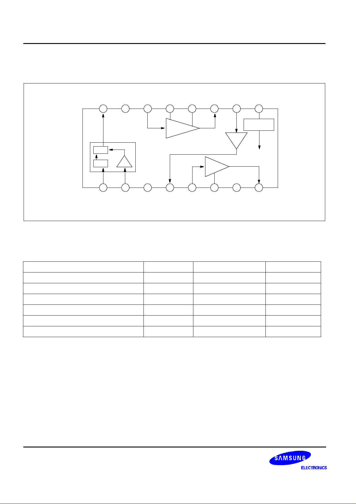
BLOCK DIAGRAM
AM IF
OUTPUTRFGND
4 3 2 1
AM F/E
MIX
RFOSC
5 6
AM OSC AM RF
INPUTRFBYPASS
AM/FM
IF INPUTIFBYPASS
7 8 9 10 11 12
AUDIO
DET OUT
ABSOLUTE MAXIMUM RATINGS (Ta = 25°C)
Character istic Symbol Value Unit
AM/FM
IF
AFC AGC
BYPASS
16 15 14 13
AUDIO
POWER
AM/FM
IF OUTPUT
POWER
AMP
RIPPLE
REJECTION
IF DET
INPUT
AM/FM
DET
AUDIO
GND
V
CC
VOLTAGE
REGULATOR
AUDIO
POWER OUT
Supply Voltage V
Power Dissipation P
Supply Current I
Thermal Resistance Junction to Ambient R
Operating Temperature T
Storage Temperature T
CC
D
CC
100 °C/W
EJA
−20 − +70 °C
OPR
STG
13 V
600 mW
44 mA
−55 − +150 °C
2

AM/FM 1 CHIP RADIO S1A0427B01
ELECTRICAL CHARACTERISTICS
(Ta =25°C, VCC = 5.5V, fm = 1kHz, AM: f = 1MHz, 30% Mod, FM: f = 10.7MHz
∆f = 22.5kHz, unless otherwise specified)
Characteristic Symbol Test Conditions Min. Typ. Max. Unit
FM
AM
PWR
AMP
Quiescent Circuit
Current
Pin 16 Terminal Voltage V
-3 dB Limiting Sensitivity V
Internal Regulated Vtg. V
Pin 16 Voltage V
Maximum Sensitivity S
I
CCQ
16(FM)
I(LIM)
CC
16 (AM)
MAX
Signal to Noise Ratio S/N
Output Power P
Total Harmonic
Distortion
O
THD
Voltage gain G
SW: FM, Vcc = 3V 7 12 17
SW: FM, Vcc = 9V 10 17 23
SW: FM, Vcc = 9V, VI = 0 2.0 2.4 3.1 V
SW: FM, −3dB
V16 = 2.4V, VR Min
− 57 − dB
SW: AM, ICC = 42mA 12 13.2 14.0 V
SW: AM, VCC = 9V, VI = 0 1.4 − 1.9 V
SW: AM, VCC = 12V
VI = 37dBµ, RL = 8Ω
VI = 37.5dBµ, RL = 8Ω
PO = 50mW
f = 1kHz, THD = 10%
VR Min, RL = 8Ω
ICC = 42mA, RL = 45Ω
f = 1kHz, VO = 2V VR Min
f = 1kHz, RL = 8Ω, PO = 50mW − 41 − dB
V
1.5 3.0 − V
15 20 − dB
0.28 − − W
− 0.5 4.0 %
mA
3

S1A0427B01 AM/FM 1 CHIP RADIO
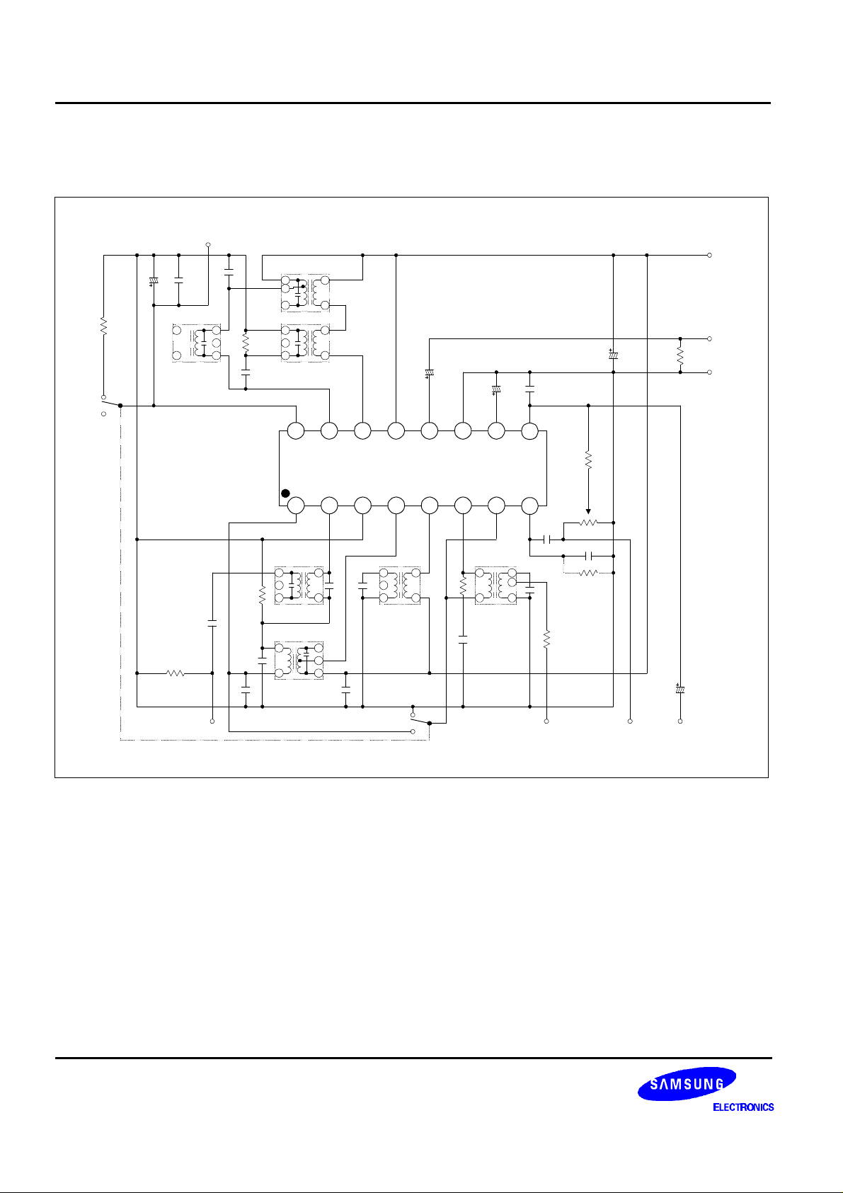
TEST CIRCUIT
V16
VCC
POWER
OUTPUT
RL
GND
1.2k
T6
6
4.7k
C15
10pF
1
2
4
3
4
3
R8
2
Ω
6
1
T5
14 1316 15
S1A0427B01
C13
470µF
12 11 10
C12
220µF
0.001µF
9
C11
22k
R6
Ω
C11
470µF
C18
C16
0.047µF
4
6
470pF
T4
3
2
1
C17
470µF
R8
Ω
SWFM
AM
1 2 3 4 7
T2
1
2
R2
3
10k
Ω
2pF
R1
50
Ω
FM IF INPUT AM RF INPUT
C3
220pF
C2
0.022µF
T3
4
6
6
4
1
2
3
C4
0.022µF
C5
680pF
C6
51pF
1
2
3
5 6
L1
6
4
FM
SW
AM
463
R3
50
Ω
C7
0.047µF
8
L2
2
1
50pF
C10
0.022µF
C8
VR
100k
Ω
0.01µF
R5
8
(R = )
R4
50
Ω
C19
3.3µF
AUDIO
DET OUTPUT
AUDIO
POWER INPUT
4

AM/FM 1 CHIP RADIO S1A0427B01
APPLICATION INFORMATION
— EXTERNAL COMPONENTS
Part
Number
R5 Am gain Control
R7
R8 FM gain adjust 470Ω Low FM gain
C2 IF bypass 0.022µF Should not be less than 0.005µF
C4 IF filter 0.022µF Removal may cause IF oscillation No influence
C7 AM bypass 0.047µF Low gain
C9 Detector filter 0.01µF Unstable IF AMP oscillation
C10 Audio coupling 0.022µF
C11
Purpose Typical
FM detector
damper
Audio Input Highcut
Smaller Than Typ Greater Than Typ
47kΩ
(33K − ∞ )
4.7kΩ
0.001µF Audio oscillation Poor response
Low AM gain
Low detector output, stable IF gain,
low FM gain
Lower sensitivity, poor low frequency
response
Influence
AGC Distortion increase,
High gain
Sharp IF AMP curve
High gain, but noise
increase
High IF Gain,
S/N ratio degrade
Using over 1 will cause
FM distortion at small
signal
Poor FM frequency
response
Bass boost affects
de-emphasis curve
C12 Ripple filter 220µF Poor frequency response & Low gain Improve AC Hum
C13
C14 Power line filter 470µF Poor AC Hum Improve AC Hum
C15
C16
C17
Audio output
coupling
FM detector
phase-shift
High freq.
(IF) bypass
AN AGC time
constant and high
frequency (IF)
bypass
470µF Poor low frequency response
10pF Narrow IF bandwidth Wide IF bandwidth
0.047µF Removal will cause fm oscillation No influence
0.047µF Charging not recommended −
Can achieve optimum
output power
5
 Loading...