

Page 1

Troubleshooting
Samsung Electronics 6-1
6. Troubleshooting
6-1 No Raster(Board Change in PDP Monitor)
ST- BY Mode(LED:RED)
Pow er On
8J1
Repl ace scal er B ’d
(LED:GREEN)
Output
or Go to Page 7- 2
SM PS
AC
Output Voltage
Input
Logic Connect Pow er Replace SMPS
LED Light- on
(Power,Sink)
X- B’d Connect Power
X- B’d
Output
Y- B’d Connect Power
Y- B’d
Output
Rep l ace Panel
ST 5V
normal
normal
Abnormal
normal
Change Fuse
normal
Abnormal Abnormal
normal
normal
Replace Logic B’d
Abnormal
normal
Replace X- B’d
Abnormal
Replace X- B’d
normal
Abnormal
Abnormal
Page 2
6-2 Samsung Electronics
Alignment and Adjustments
6-2 No Raster in Scaler Board
Normal
Abnormal
Abnormal
Normal
Abnormal
Normal
Abnormal
Normal
Abnormal
Abnormal
Normal
Normal
Check Input Signal of U38 uPD64082
Pin 88(CVBSin)
CHECK
UPD64082
CHECK INPU T SIGINA L
Check Input Signal of 3U1 VPC3230
Pin 75(Y IN)
Check Output Signal of 3U3 SDA9280
Pin 47(Yout),
Check Input Signal of 1U1 AD9884
R,G,B IN A ND H,V IN
Normal
Check Output Signal of 1U1 AD9884
Pin 115(CLK), 85(G7), 105(R7),65(B7)
Check Input Signal of 5U1 LV DS IC
Pin 2 7(L H S),28(L V S),32(CL K )
Check Output Data of 5J1
Check 3U1,
3U2 OR3U3
CHECK 2U2
CXA 2101
CHECK 1U1
AD9884
CHECK
PW364
Check 5U1
LVDS IC
Check Logic B’d
Page 3

Troubleshooting
Samsung Electronics 6-3
6-3 Checking the Board (Unit)
Page 4

Troubleshooting
6-4 Samsung Electronics
6-4 50” HD D1.0 Logic Main Board T/S
If the PDP unit and the logic board operates properly, the operation LED of Figure 1 would blink at about
1 second interval.
If the unit is out of order, check the status of the operation LED through eye-inspection first.
If the behavior of the operation LED is different from that of normal state, you have to replace the board.
To check the trouble on the board, complete the following logic board test procedures described below.
Required testing equipment : - Oscilloscope (digital 400 MHz with more than 3 channels)
- Multi-meter
Other equipment : - DC power supply (5V: 1EA)
- Sub-PCB ASS'Y for JIG: 1 EA
① First, perform eye-inspection and short-circuit inspection for the power stage of the target logic
board. Then, perform the following tests on the board in sequence if no problem has been found.
② Replace the (Serial EEPROM) on the logic board with the Test EERPOM.
Change the clock setting of the logic board to internal.
(Refer to the configuration procedures in the next page)
If the Test EEPROM is not available, perform the tests by installing key scan and set the address
number 9F to 00.
➂ Implement 5V to the LD1, and check if the LED on the left-top of the board blinks at about one
second intervals.
➃ If the LED blinks too fast or the LED is not turned on, it means that the LOGIC board is not operating
properly.
➄ If no problem is found in the above step, connect sub-PCB to check the logic output. Then measure
the output waveform of the sub-PCB, and compare it with the appended waveform in normal state.
Record the test result (OK or NG).
➅ Check drive Y s/w , drive X s/w , and address signals in that order.
⑦ Set probe 1 of the oscilloscope to the trigger signal, and connect it to TP105 on the logic board.
➇ Set the oscilloscope to 2ms/div. After adjusting probe 2 to 5V/div, check the output signal.
⑨ After T/S, turn off the power supply, and disconnect the connector.
➉ Record the test result on the test sheet.
Page 5

Troubleshooting
Samsung Electronics 6-5
6-4-1 Data : No6~15 at LE2001, LE2002, LE2003, LG2001, LG2002, LG2003
: No28~33 at LG2003
: No35~40 at LE2003
6-4-2 POL : No25 at LE2001, LE2002, LE2003, LG2001, LG2002, LG2003
Page 6

Troubleshooting
6-6 Samsung Electronics
6-4-3 STB: No24 at LE2001, LE2002, LE2003, KG2001, KG2002, LG2003
6-4-4 CLK : No12,22 at LE2001, LE2002, LE2003, LG2001, LG2002, LG2003
Page 7

Troubleshooting
Samsung Electronics 6-7
6-4-5 Y5
6-4-6 Y7
Page 8

Troubleshooting
6-8 Samsung Electronics
6-4-7 Y9
6-4-8 Y11
Page 9

Troubleshooting
Samsung Electronics 6-9
6-4-9 Y13
6-4-10 Y15
Page 10

Troubleshooting
6-10 Samsung Electronics
6-4-11 Y17
6-4-12 Y19
Page 11

Troubleshooting
Samsung Electronics 6-11
6-4-13 Y21
6-4-14 Y23
Page 12

Troubleshooting
6-12 Samsung Electronics
6-4-15 Y25
6-4-16 Y28
Page 13

Troubleshooting
Samsung Electronics 6-13
6-4-17 Y30
6-4-18 Y32
Page 14

Troubleshooting
6-14 Samsung Electronics
6-4-19 Y34
6-4-20 X2
Page 15

Troubleshooting
Samsung Electronics 6-15
6-4-21 X4
6-4-22 X6
Page 16

Troubleshooting
6-16 Samsung Electronics
6-4-23 X8
6-4-24 X10
Page 17

Troubleshooting
Samsung Electronics 6-17
6-5 50” HD Logic Buffer Board T/S
Required testing equipment : - Oscilloscope (digital 400 MHz with more than 2 channels)
Other equipment : - DC power supply (5V: 1EA)
- Multi-meter
- Logic board: 1EA
- Sub-PCB ASS'Y for JIG: 1 EA
! First perform eye-inspection and short-circuit inspection for the power stage of the logic board to
test. Then, perform the following tests on the board in sequence if no problem has been found.
@ If no problem was found in step ! connect the buffer board as [Figure2.3] shows. Then connect
the sub-PCB to check COF data and replace the serial EEPROM with the Test EEPROM so the
output pattern of the logic board becomes a full-white pattern.
# If the Test EEPROM is not available, then perform the tests by installing key scan, and setting
the address number 9F to 00.
$ Supply 5V to the logic board, and check that the LED on the left-top of the board blinks at about
1 second intervals. If no problem is found, measure the output waveform of the sub-PCB, and
compare it with the appended waveform of normal state.
% Checking order; ECN3001, ECN3002, ECN3003, FCN3104, FCN3105, FCN3106,FCN3107, FCN3108,
GCN3209, GCN3210, GCN3211, HCN3312, HCN3313, HCN3314, ICN3415, ICN3416, ICN3417,
ICN3418, ICN3419, JCN3520, JCN3521, and JCN3522. You can also check only the doubtable
waveforms selectively.
^ Set probe 1 of the oscilloscope to trigger signal, and connect it to the TP105 of the logic board.
Set the oscilloscope to 2ms/div. You can magnify the important points to check in details.
After adjusting probe 2 to 5V/div, check the output signal.
& The appended waveform is when a full-white input pattern is implemented.
* After T/S, turn off the power supply and disconnect the connector. Then record the result on the
examination sheet.
Page 18

Troubleshooting
6-18 Samsung Electronics
LOGIC MAIN BOARD & LOGIC BUFFER BOARD(E,F,G) CONNECTION
LOGIC MAIN BOARD & LOGIC BUFFER BOARD(H,I,J) CONNECTION
Page 19

Troubleshooting
Samsung Electronics 6-19
6-5-1 DATA-IG No(13~18, 49~45)
6-5-2 POL Signal-Jig No(20, 27, 56, 63)
Page 20

Troubleshooting
6-20 Samsung Electronics
6-5-3 Magnified POL(Magnifying the Above Signal)
6-5-4 STB-Jig No(25, 32, 61, 68)
Page 21

Troubleshooting
Samsung Electronics 6-21
6-5-5 Magnified STB(Magnifying the Above Signal)
6-5-6 CLK-Jig No(24, 31, 60, 67)
Page 22

Troubleshooting
6-22 Samsung Electronics
6-5-7 Magnified CLK
Page 23

Troubleshooting
Samsung Electronics 6-23
6-6 Driver Board T/S
6-6-1 Main X Board Layout and T/S TP point
CN4007
CN4006
R4031
TP5
R4001 T P1
R4015
TP3
400
R4035
TP4
R4044
TP2
210
Page 24

Troubleshooting
6-24 Samsung Electronics
6-6-2 Main y Board Layout and T/S TP point
TPOUT1
TPSI
TPPOL
TPBLK
TPSTB
TPCLK
CN5008
TPSI
TPPOL
TPBLK
TPSTB
TPCLK
M5014
TP7
M5037
TP8
ZD5002
TP6
R5029
TP1
R5001
TP3
400
R5035
TP5
300
R5077
TP9
R5052
TP2
R5083
TP4
260
60
Page 25

Troubleshooting
Samsung Electronics 6-25
6-6-3 Input Power
Pin#
1
2
3
4
5
6
7
8
9
10
11
12
Voltage Source
Vcc1=5V
GND
Vcc2=17V
GND
Ve=0V
GND
NC
GND
GND
Vs=168V
Vs=168V
Vs=168V
CN4007
Pin#
1
2
3
4
5
6
7
8
9
10
11
12
13
Voltage Source
Vcc1=5V
GND
Vcc2=17V
GND
Vscan=70V
GND
Vset=210V
NC
GND
GND
Vs=168V
Vs=168V
Vs=168V
CN5008
Page 26

Troubleshooting
6-26 Samsung Electronics
6-6-4 Drive Board Troubleshooting
:The following measures are troubleshooting procedures in case of SET troubles, due to the drive board
problem.
l If SMPS shutdown is blocked.
- Find out which board is faulty by connecting the power ports of the X/Y board one by one.
: Check the resistance between the drain and the source of the FET on the faulty board.
In case of a short, replace the corresponding FET.
: Check for a short between the input voltage ports (CN4007 and CN5008) and the GND of the
faulty board.
l If the discharge screen is in trouble (Discharge trouble):
- Check that the Scan output voltage of the power output port is between 70V and 85V.
- Check the resistance between the drain and the source of the FET (M5014) on the Y board.
If they are short, replace the FET.
- Checking the operation of the drive buffer board:
: Check the resistance between the Test Points [OUT_L ~ OUT_H]. In case of a short, replace the
buffer board.
- Checking the connectors:
: Check CN5002 (Y board), and CN4008 (X board) to ensure if they are connected properly.
l When driving screen, horizontally adjacent 2 lines are emitting.
- Check if there is extraneous substance or inappropriate soldering, which may occur a short
around the IC output lines in question on the drive buffer board.
l When the drive board does not operate
(The LED of the logic board blinks, but nothing appears on the screen):
- Check that the drive board input stage is installed in the connector properly.
- Check if the fuses (F4001, F4002, F5001, and F5002) are blown.
Page 27

Troubleshooting
Samsung Electronics 6-27
6-7 Troubleshooting when the SMPS is out of order
1. Check that auxiliary power (5VSB) is detected.
1.1 If auxiliary power is not detected, check if BRD101S is a short.
2. If it is in shutdown state;
2.1 Check that each output is a short.
2.2 Check if the protection circuit has a problem.
3. If output voltage (except auxiliary power) is not detected, check as follows.
3.1. If VS voltage is not detected
3.1.1 When the FUSE is blown --> Check that FET (Q5S and Q6S) is a short.
Check that FET (Q308 ~ Q311) is a short.
Check that BRD1S is a short.
3.1.2 If DC5V RELAY (RL1S, RL2S) does not operate, check that auxiliary power (5VSB) is detected.
3.1.3 If DC24V RELAY (RL3S) does not operate, check if F1 is blown.
3.2 In case of +5V (D), check if D305 is short.
3.3 In case of VSAMP, check if D509 is short.
3.4 In case of VA, check if D303 is short.
3.5 In case of VSET, VE, and VSCAN, check if VS voltage is detected and if F501 is blown.
Page 28

Troubleshooting
6-28 Samsung Electronics
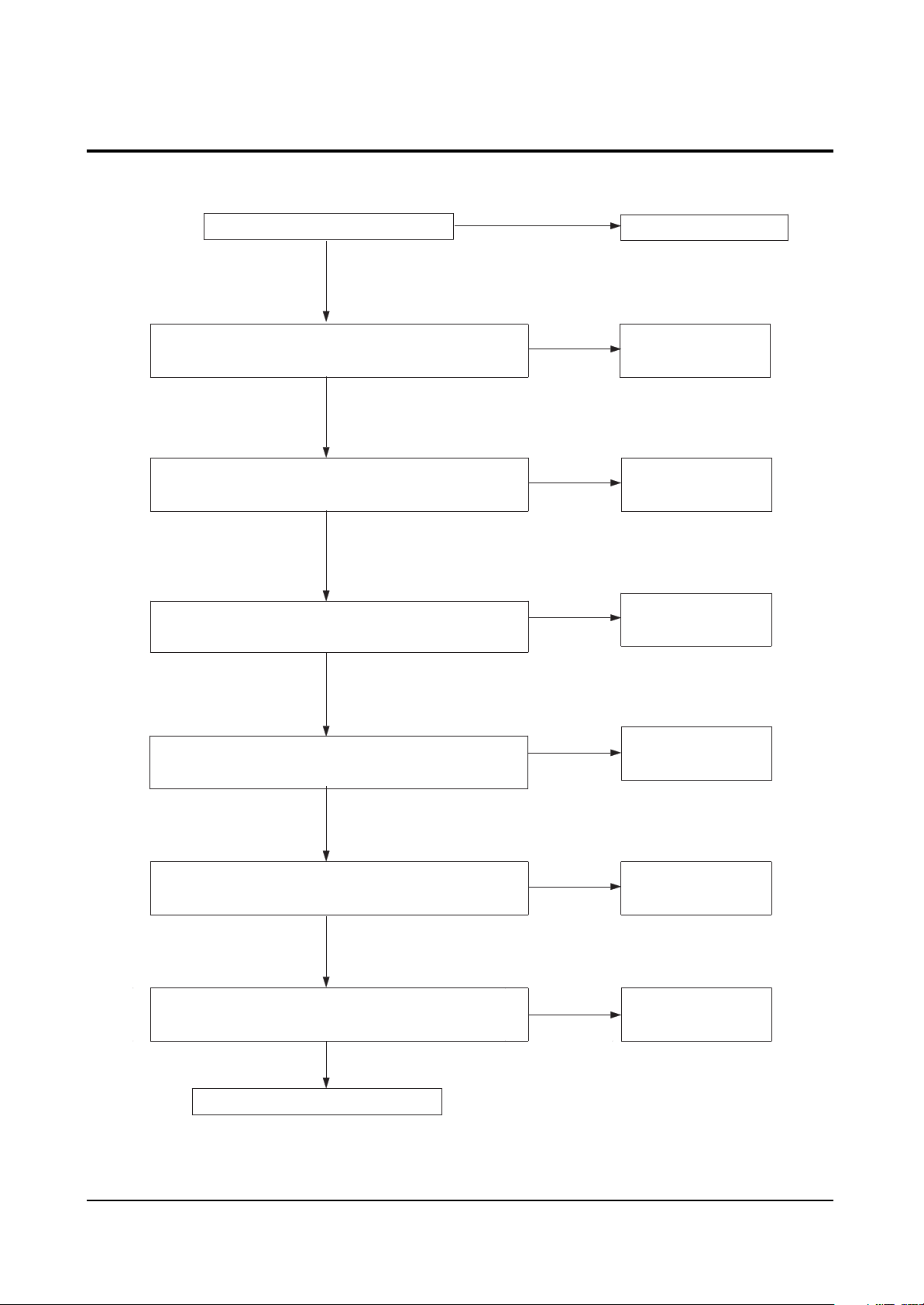
6-8 No audio is sounded and video is displayed properly
Check the voltage of pin3(9V)
and the voltage between pin 6 and
7(12V) of CN602.
Normal
Supply noise to C668
or C669(+) terminal.
Normal
Check the circuitry
around IC601.
Abnormal
Check the output voltage
of SMPS Ass’y.
Abnormal
Check the circuitry
around IC602 and
the connectivity between
the speakers and
the jacks of the unit.
 Loading...