

Page 1

SGS0WHOHYLVLRQ FRQWHQWV
1. Precaution
2. Product Specification
3. Disassembly & Reassembly
4. Troubleshooting
5. Exploded View & Part List
6. Wiring Diagram
7. Schematic Diagram
VHUYLFH
Pdqxdo
PS-42C96HD
PS-50C96HD
SGS0WHOHYLVLRQ
Fkdvvlv = I63D+SbHxurshbKG,bOlo|#
Prgho = SV75F<9KG[2[HF#
SV83F<9KG[2[HF
Refer to the service manual in the GSPN (see the rear cover) for the more information.
Page 2

This Service Manual is a property of Samsung Electronics Co.,Ltd.
Any unauthorized use of Manual can be punished under applicable
International and/or domestic law.
© Samsung Electronics Co., Ltd. Apr. 2007
Printed in Korea
AA82-04399A
Area Web Site
North America service.samsungportal.com
Latin America latin.samsungportal.com
CIS cis.samsungportal.com
Europe europe.samsungportal.com
China china.samsungportal.com
Asia asia.samsungportal.com
Mideast & Africa mea.samsungportal.com
GSPN (Global Service Partner Network)
Page 3

Table of Contents
Chapter 1 Precaution
■ 1-1 Safety Precautions . . . . . . . . . . . . . . . . . . . . . . . . . . . . . . . . . . . . . . . . . . . . . . . . . . . . . . . . . . . 1-1
■ 1-2 Servicing Precautions . . . . . . . . . . . . . . . . . . . . . . . . . . . . . . . . . . . . . . . . . . . . . . . . . . . . . . . . 1-3
■ 1-3 Static Electricity Precautions . . . . . . . . . . . . . . . . . . . . . . . . . . . . . . . . . . . . . . . . . . . . . . . . . . . 1-4
■ 1-4 Installation Precautions . . . . . . . . . . . . . . . . . . . . . . . . . . . . . . . . . . . . . . . . . . . . . . . . . . . . . . . 1-5
Chapter 2 Product Specification
■ 2-1 Product Specification . . . . . . . . . . . . . . . . . . . . . . . . . . . . . . . . . . . . . . . . . . . . . . . . . . . . . . . . . 2-1
■ 2-2 Specifications Analysis . . . . . . . . . . . . . . . . . . . . . . . . . . . . . . . . . . . . . . . . . . . . . . . . . . . . . . . . 2-2
■ 2-3 Accessories . . . . . . . . . . . . . . . . . . . . . . . . . . . . . . . . . . . . . . . . . . . . . . . . . . . . . . . . . . . . . . . . 2-3
Chapter 3 Disassembly & Reassembly
■ 3-1 Overall Disassembly & Reassembly . . . . . . . . . . . . . . . . . . . . . . . . . . . . . . . . . . . . . . . . . . . . . 3-1
Chapter 4 Troubleshooting
■ 4-1 Troubleshooting . . . . . . . . . . . . . . . . . . . . . . . . . . . . . . . . . . . . . . . . . . . . . . . . . . . . . . . . . . . . . 4-1
■ 4-2 Adjustment . . . . . . . . . . . . . . . . . . . . . . . . . . . . . . . . . . . . . . . . . . . . . . . . . . . . . . . . . . . . . . . . . 4-16
■ 4-3 Upgrade . . . . . . . . . . . . . . . . . . . . . . . . . . . . . . . . . . . . . . . . . . . . . . . . . . . . . . . . . . . . . . . . . . . 4-32
Chapter 5 Exploded View & Part List
■ 5-1 PS42C96HDX/XEC Exploded View . . . . . . . . . . . . . . . . . . . . . . . . . . . . . . . . . . . . . . . . . . . . . . 5-1
■ 5-2 PS50C96HDX/XEC Exploded View . . . . . . . . . . . . . . . . . . . . . . . . . . . . . . . . . . . . . . . . . . . . . . 5-3
■ 5-3 PS42C96HDX/XEC Service Item . . . . . . . . . . . . . . . . . . . . . . . . . . . . . . . . . . . . . . . . . . . . . . . . 5-5
■ 5-4 PS50C96HDX/XEC Service Item . . . . . . . . . . . . . . . . . . . . . . . . . . . . . . . . . . . . . . . . . . . . . . . . 5-6
Chapter 6 Wiring Diagram
■ 6-1 Overall Wiring . . . . . . . . . . . . . . . . . . . . . . . . . . . . . . . . . . . . . . . . . . . . . . . . . . . . . . . . . . . . . . . 6-1
Chapter 7 Schematic Diagram
■ 7-1 Circuit Description . . . . . . . . . . . . . . . . . . . . . . . . . . . . . . . . . . . . . . . . . . . . . . . . . . . . . . . . . . . 7-1
■ 7-2 Schematic Diagram . . . . . . . . . . . . . . . . . . . . . . . . . . . . . . . . . . . . . . . . . . . . . . . . . . . . . . . . . . 7-3
Page 4

Part Name Description Description Photo
Cover
Rear
Disassembly & Reassembly
Samsung Electronics 3-1
3. Disassembly & Reassembly
3-1 Overall Disassembly & Reassembly
3-1-1 Separation of ASSY COVER P-REAR
3-1-2 Separation of ASSY PCB MISC-MAIN
Part Name Description Description Photo
Main
Board
① Detach all connectors from the Main
Board.
② Remove 4 screws.
: PH,+,WWP,M3,L8,NI PLT
③ Remove the Main Board.
Notice
- Be sure to separate the power cord before disassembling the unit.
- Discharge the capacitors first when separating PCB's with high capacity capacitors such as SMPS, X Main Board, YMain
Board, etc. (Aspark may be generated by the electric charge, and there is danger of electronic shock.)
- Check that the cables are properly connected referring to the circuit diagram when disassembling or assembling the unit
taking care not to damage the cables.
- Take care not to scratch the Glass Filter in the front.
- Assemble the boards in the reverse order of the disassembly.
- The plasma must be layed down on a flat padded surface for disassembly and reassembly.
① Remove 4 screws. ( )
: M8,L16,ZPC(BLK),SWRCH18A,WP
② Remove 15 screws. ( )
: BH,+,B,M4,L3,ZPC(BLK)
③ Remove 4 screws. ( )
: PH,+,WSP,S,M4,L35,ZPC(BLK)
④ Remove the 2 Hex nuts for the PC
input. ( )
: #4-40,L6,NI PLT,C3601,-
⑤ Remove the Cover Rear.
: Please lay the PDP unit face down on a
soft surface when removing the stand.
Page 5

Disassembly & Reassembly
3-2 Samsung Electronics
3-1-3 Separation of FILTER-EMI AC LINE
Part Name Description Description Photo
FILTER-
EMI
AC LINE
① Detach connector from Main SMPS.
② Remove 2 screws. ( )
: PH,+,WWP,M3,L8,NI PLT
③ Remove a screw. ( )
: BH,+,S,M4,L10,ZPC(BLK)
④ Remove FILTER-EMI AC LINE.
3-1-4 Separation of BRACKET-PCB
Part Name Description Description Photo
Bracket
PCB
① Remove a screw.
: BH,+,S,M4,L10,ZPC(BLK)
② Remove the BRACKET-PCB.
Page 6

Disassembly & Reassembly
Samsung Electronics 3-3
3-1-5 Separation of ASSY BRACKET
Part Name Description Description Photo
42"
Bracket
① Remove 4 screws. ( )
: BH,+,S,M4,L10,ZPC(BLK)
② Remove 2 screws. ( )
: BH,+,B,M4,L3,ZPC(BLK)
③ Remove Bracket.
50"
Bracket
① Remove 4 screws. ( )
: BH,+,S,M4,L10,ZPC(BLK)
② Remove 2 screws. ( )
: BH,+,B,M4,L3,ZPC(BLK)
③ Remove Bracket.
3-1-6 Separation of ASSY BOARD P-SIDE AV
Part Name Description Description Photo
Side AV
① Remove a screw. ( )
: BH,+,B,M4,L3,ZPC(BLK)
② Remove a screw. ( )
: BH,+,S,M4,L10,ZPC(BLK)
③ Remove the Side AV.
Page 7

Disassembly & Reassembly
3-4 Samsung Electronics
3-1-7 Separation of ASSY BRACKET P-WALL
Part Name Description Description Photo
42"
Wall
Bracket
① Remove 2 screws. ( )
: BH,+,B,M4,L3,ZPC(BLK)
② Remove 6 screws. ( )
: BH,+,S,M4,L10,ZPC(BLK)
③ Remove Wall Bracket.
: Please lay the PDP panel face down
on a soft surface when separating front
cover.
50"
Wall
Bracket
① Remove 2 screws. ( )
: BH,+,B,M4,L3,ZPC(BLK)
② Remove 6 screws. ( )
: BH,+,S,M4,L10,ZPC(BLK)
③ Remove Wall Bracket.
: Please lay the PDP panel face down on
a soft surface when separating front
cover.
Page 8

Disassembly & Reassembly
Samsung Electronics 3-5
3-1-8 Separation of ASSY SPEAKER P
Part Name Description Description Photo
42"
Speaker
① Remove 4 screws.
: BH,+,WP,B,M4.0,L3,ZPC(BLK),
SWRCH18A
② Remove the Speaker.
50"
Speaker
① Remove 4 screws.
: BH,+,WP,B,M4.0,L3,ZPC(BLK),
SWRCH18A
② Remove the Speaker.
3-1-9 Separation of ASSY BOARD P-POWER&IR
Part Name Description Description Photo
Power
&
IR Board
① Detach all connectors from the
Power&IR Board.
② Remove the Power&IR PCB unlocking
the 2 holders.
Page 9

Disassembly & Reassembly
3-6 Samsung Electronics
3-1-10 Separation of SMPS-PDP TV
Part Name Description Description Photo
42"
SMPS
① Detach all connectors from the SMPS.
② Remove 8 screws.
: PH,+,WWP,M3,L8,NI PLT
③ Remove the SMPS.
: Wear gloves when handling the power
board as there may be some remaining
electrical charge in the capacitor.
Specifically, avoid touching any part of
the capacitor.
50"
SMPS
① Detach all connectors from the SMPS.
② Remove 8 screws.
: PH,+,WWP,M3,L8,NI PLT
③ Remove the SMPS.
: Wear gloves when handling the power
board as there may be some remaining
electrical charge in the capacitor.
Specifically, avoid touching any part of
the capacitor.
Page 10
Disassembly & Reassembly
Samsung Electronics 3-7
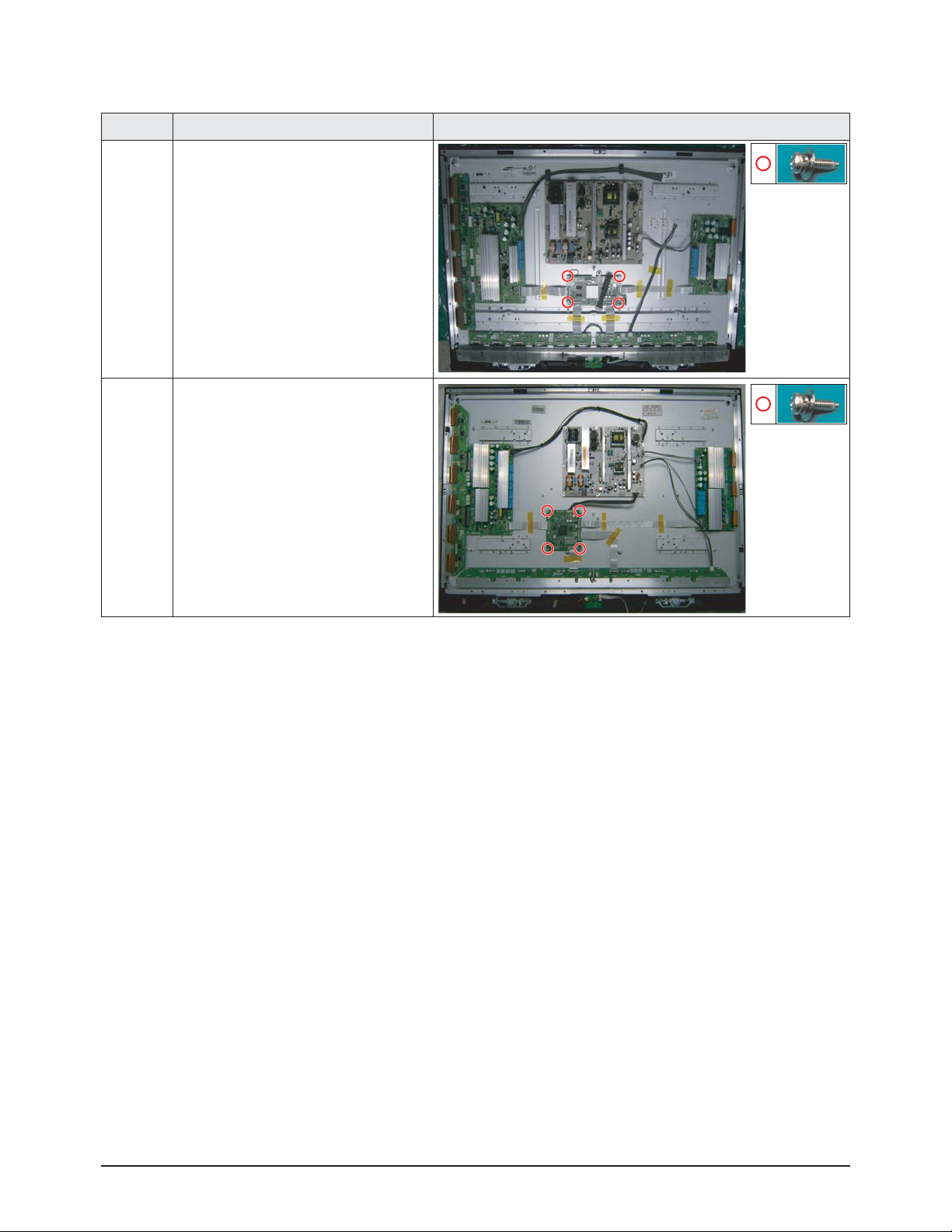
3-1-11 Separation of ASSY PDPMODULE P-LOGIC MAIN BOARD
Part Name Description Description Photo
42"
Logic
Board
① Detach all connectors from the Logic
Main Board.
② Remove 4 screws.
: WSP,PH,+,M3,L8,NI PLT
③ Remove the Logic Main Board.
50"
Logic
Board
① Detach all connectors from the Logic
Main Board.
② Remove 4 screws.
: WSP,PH,+,M3,L8,NI PLT
③ Remove the Logic Main Board.
Page 11

Disassembly & Reassembly
3-8 Samsung Electronics
3-1-12 Separation of ASSY PDP MODULE P-X MAIN BOARD
Part Name Description Description Photo
Flat Cable
42"
X-Main
Board
① Remove 4 screws.
: PH,+,WWP,M3,L8,NI PLT
② Remove the X-Main Board.
50"
X-Main
Board
① Remove 4 screws.
: PH,+,WWP,M3,L8,NI PLT
② Remove the X-Main Board.
① Detach all Connectors from the X-Main
Board.
※ To separate the Flat Cable of the
X-Board, press the upper and the lower
sides of the connector.
Page 12

Disassembly & Reassembly
Samsung Electronics 3-9
3-1-13 Separation of ASSY PDP MODULE P-Y MAIN BOARD
Part Name Description Description Photo
Flat Cable
① Detach the 6 scan board connectors
from the panel by pulling the holder from
both the top and bottom ends.
42"
Y-Scan
Board
① Remove 3 screws.
: PH,+,WWP,M3,L8,NI PLT
50"
Y-Scan
Board
① Remove 5 screws.
: PH,+,WWP,M3,L8,NI PLT
Page 13

Disassembly & Reassembly
3-10 Samsung Electronics
Part Name Description Description Photo
42"
Y-Main
Board
① Remove 4 screws.
: PH,+,WWP,M3,L8,NI PLT
② Detach all connectors from the Y-Main
Board.
50"
Y-Main
Board
① Remove 4 screws.
: PH,+,WWP,M3,L8,NI PLT
② Detach all connectors from the Y-Main
Board.
Page 14

Disassembly & Reassembly
Samsung Electronics 3-11
3-1-14 Separation of ASSY PDP MODULE P-ADDRESS BUFFER BOARD
Part Name Description Description Photo
42"
Still Bar
50"
Still Bar
42"
Buffer
Board
① Detach the all connectors from the
buffer board.
② Remove 3 screws.
: PH,+,WWP,M3,L8,NI PLT
③ Remove the E-Board and F-Board.
50"
Buffer
Board
① Detach the all connectors from the
buffer board.
② Remove 14 screws.
: PH,+,WWP,M3,L8,NI PLT
③ Remove the E-Board and F-Board.
① Remove 4 screws.
: PH,+,WWP,M3,L8,NI PLT
② Remove the Still Bar.
① Remove 4 screws.
: PH,+,WWP,M3,L8,NI PLT
② Remove the Still Bar.
Page 15

3-1-16 Separation of ASSY PCB FUNCTION
Part Name Description Description Photo
Function
Board
Disassembly & Reassembly
3-12 Samsung Electronics
3-1-15 Separation of ASSY PANEL BRACKETS
Part Name Description Description Photo
Panel
Brackets
① Remove 3 screws. ( )
: BH,+,B,M4,L3,ZPC(BLK)
② Remove 4 screws. ( )
: BH,+,S,M4,L10,ZPC(BLK)
③ Remove the Side Panel Brackets.
① Remove 2 screws.
: BH,+,B,M4,L3,ZPC(BLK)
② Remove the Function Board.
Page 16

Samsung Electronics5-1
Exploded View & Part List
5. Exploded View & Part List
5-1 PS42C96HDX/XEC Exploded View
M0013
T0079T0915
M0412
M0020
M0027
T0268
T0044
M0149
T0456
M0146
M0105
T0175
M0145
M0150
M0105
M0112
T0074
T0003
M0146
T0023
T0056
CIS7
T0023
Page 17

5-2Samsung Electronics
Exploded View & Part List
Loc. No. Code No. Description Specification Q'ty SA/SNA Remark
CIS7 AA61-60003B SPRING ETC-CS -,SUS304,-,-,OD11.2,N7,OD1 1 S.N.A
M0013 BN96-04709B ASSY COVER P-REAR 42Q9/C9,EU(iDTV),PCM T 1 S.A
M0020 BN96-04900D ASSY BOARD P-SIDE A/V LILY 42",SJ06-01-0 1 S.N.A
M0027 BN96-05835A ASSY STAND P-BASE 42Q9/42C9,ABS,SF-0507, 1 S.A
M0105 BN67-00190A LENS-LED 42Q9,PC,light blue,Material of 1 S.N.A
M0112 BN63-03047D COVER-FRONT 42C9,ABS,HB,BK23,STEAM MOLD 1 S.N.A
M0145 BN96-04853B ASSY BOARD P-FUNCTION Lily/Calla,CT5000- 1 S.A
M0146 BN96-04687A ASSY BRACKET P-FILTER SIDE 42Q9,AL6063,T 2 S.N.A
M0146 BN96-04861D ASSY BOARD P-POWER & IR Lily/Calla,CT500 1 S.A
M0149 BN96-04685A ASSY BRACKET P-FILTER TOP 42Q9,AL6063,T1 1 S.N.A
M0150 BN96-04686A ASSY BRACKET P-FILTER BOTTOM 42Q9,AL6063 1 S.N.A
M0150 BN96-04691B ASSY BRACKET P-SUPPORT FILTER 42Q9,Al 60 1 S.N.A
M0412 BN96-04903C ASSY BRACKET P-PCB 42Q9,SECC T0.8 1 S.N.A
T0003 BN96-04712D ASSY COVER P-FRONT 42C9,ABS HB,BK23,STEA 1 S.A
T0023 BN96-04707A ASSY COVER P-KNOB POWER C9/Q9,ABS HB 1 S.A
T0023 BN64-00567A KNOB POWER 42Q9,PC,VIOLET 1 S.N.A
T0044 BN96-04592A ASSY PDP MODULE P-MODULE 42HD W2,PL42AX0 1 S.A
T0056 BN63-03091A COVER-DECORATION 42C9,ABS,HB,BLK 1 S.N.A
T0074 BN59-00611A REMOCON JASMINE , LILY,TM87C,SAMSUNG 28p 1 S.A
T0079 BN94-01221C ASSY PCB MISC-MAIN PS42C96HD,F30A,BN41-0 1 S.N.A
T0175 BN96-04704A ASSY SPEAKER P 8ohm,C9,10W,4P connector, 1 S.A
T0268 3903-000145 CBF-POWER CORD DT,EU,FP3/YES,U(IEC C13-R 1 S.A
T0456 BN67-00188A GLASS-FILTER EMI 42" C7 HD,Sputter,with 1 S.A
T0915 BN61-02894B HOLDER-MODULE 42Q9,PC ABS 2 S.N.A
Page 18

Samsung Electronics5-3
Exploded View & Part List
5-2 PS50C96HDX/XEC Exploded View
M0013
T0079
M0412
M0020
T0044
T0915
M0149
M0146
T0456
M0027
M0105
T0268
T0074
T0003
M0146
T0023
T0175
M0145
M0150
M0105
M0112
T0056
CIS7
T0023
Page 19

5-4Samsung Electronics
Exploded View & Part List
Loc. No. Code No. Description Specification Q'ty SA/SNA Remark
CIS7 AA61-60003B SPRING ETC-CS -,SUS304,-,-,OD11.2,N7,OD1 1 S.N.A
M0013 BN96-04711B ASSY COVER P-REAR 50Q9/C9,EU(iDTV),PCM T 1 S.A
M0020 BN96-04900E ASSY BOARD P-SIDE A/V LILY 50",SJ06-01-0 1 S.N.A
M0027 BN96-04714B ASSY STAND P-BASE C9/Q9,ABS HB SF-0507,B 1 S.A
M0105 BN67-00190A LENS-LED 42Q9,PC,light blue,Material of 1 S.N.A
M0112 BN63-03067D COVER-FRONT 50C9,ABS,HB,BK23,STEAM MOLD 1 S.N.A
M0145 BN96-04853B ASSY BOARD P-FUNCTION Lily/Calla,CT5000- 1 S.A
M0146 BN96-04690A ASSY BRACKET P-FILTER SIDE 50Q9,AL6063,T 2 S.N.A
M0146 BN96-04861D ASSY BOARD P-POWER & IR Lily/Calla,CT500 1 S.A
M0149 BN96-04688A ASSY BRACKET P-FILTER TOP 50Q9,AL6063,T1 1 S.N.A
M0150 BN96-04692A ASSY BRACKET P-SUPPORT FILTER 50Q9,AL606 1 S.N.A
M0150 BN96-04689A ASSY BRACKET P-FILTER BOTTOM 50Q9,AL6063 1 S.N.A
M0412 BN96-04903C ASSY BRACKET P-PCB 42Q9,SECC T0.8 1 S.N.A
T0003 BN96-04713D ASSY COVER P-FRONT 50C9,ABS HB,BK23,STEA 1 S.A
T0023 BN96-04707A ASSY COVER P-KNOB POWER C9/Q9,ABS HB 1 S.A
T0023 BN64-00567A KNOB POWER 42Q9,PC,VIOLET 1 S.N.A
T0044 BN96-05772A ASSY PDP MODULE P PL50HW025A,50HD W2A,PL 1 S.A
T0056 BN63-03081A COVER-DECORATION 50C9,ABS,HB BLK 1 S.N.A
T0074 BN59-00611A REMOCON JASMINE , LILY,TM87C,SAMSUNG 28p 1 S.A
T0079 BN94-01223C ASSY PCB MISC-MAIN PS50C96HD,MAIN,F30A,B 1 S.N.A
T0175 BN96-04704A ASSY SPEAKER P 8ohm,C9,10W,4P connector, 1 S.A
T0268 3903-000145 CBF-POWER CORD DT,EU,FP3/YES,U(IEC C13-R 1 S.A
T0456 BN67-00197A GLASS-FILTER EMI 50 W2, C9,Sputter, wit 1 S.A
T0915 BN61-02895B HOLDER-MODULE 50Q9,PCABS 2 S.N.A
Page 20

Samsung Electronics5-5
Exploded View & Part List
5-3 PS42C96HDX/XEC Service Item
Loc. No. Code No. Description Specification Q'ty Remark
M0013 BN96-04711B ASSY COVER P-REAR 50Q9/C9,EU(iDTV),PCM T 1
M0027 BN96-04714B ASSY STAND P-BASE C9/Q9,ABS HB SF-0507,B 1
M2893 BN39-00859A LEAD CONNECTOR CALLA 50",UL20276#30,UL/C 1
M2893 BN39-00881A LEAD CONNECTOR LILLY 42"/50",UL1007#26,U 1
T0003 BN96-04713D ASSY COVER P-FRONT 50C9,ABS HB,BK23,STEA 1
T0044 BN96-05772A ASSY PDP MODULE P PL50HW025A,50HD W2A,PL 1
T0074 BN59-00611A REMOCON JASMINE , LILY,TM87C,SAMSUNG 28p 1
T0079 BN94-01223C ASSY PCB MISC-MAIN PS50C96HD,MAIN,F30A,B 1
T0175 BN96-04704A ASSY SPEAKER P 8ohm,C9,10W,4P connector, 1
T0764 BN44-00162A SMPS-PDP TV HPS5053,SEM,AC/DC,460W,AC100 1
T1910 BN96-06091A ASSY PDP MODULE P-X-MAIN BOARD PL50HW025 1
T1911 BN96-06092A ASSY PDP MODULE P-Y-MAIN BOARD PL50HW025 1
T1914 BN96-06096A ASSY PDP MODULE P-ADDRESS E BU PL50HW025 1
T1915 BN96-06097A ASSY PDP MODULE P-ADDRESS F BU PL50HW025 1
T1917 BN96-06095A ASSY PDP MODULE P-LOGIC MAIN PL50HW025A, 1
T1960 BN96-06093A ASSY PDP MODULE P-Y-MAIN UPPER PL50HW025 1
T1961 BN96-06094A ASSY PDP MODULE P-Y-MAIN LOWWE PL50HW025 1
※ This is the list which is available to repair the real material at the time of service.
Page 21

5-6Samsung Electronics
Exploded View & Part List
5-4 PS50C96HDX/XEC Service Item
Loc. No. Code No. Description Specification Q'ty Remark
M0013 BN96-04709B ASSY COVER P-REAR 42Q9/C9,EU(iDTV),PCM T 1
M0027 BN96-05835A ASSY STAND P-BASE 42Q9/42C9,ABS,SF-0507, 1
M2893 BN39-00859A LEAD CONNECTOR CALLA 50",UL20276#30,UL/C 1
M2893 BN39-00881A LEAD CONNECTOR LILLY 42"/50",UL1007#26,U 1
T0003 BN96-04712D ASSY COVER P-FRONT 42C9,ABS HB,BK23,STEA 1
T0044 BN96-04592A ASSY PDP MODULE P-MODULE 42HD W2,PL42AX0 1
T0074 BN59-00611A REMOCON JASMINE , LILY,TM87C,SAMSUNG 28p 1
T0079 BN94-01221C ASSY PCB MISC-MAIN PS42C96HD,F30A,BN41-0 1
T0175 BN96-04704A ASSY SPEAKER P 8ohm,C9,10W,4P connector, 1
T0764 BN44-00161A SMPS-PDP TV HPS4253,SEM,AC/DC,370W,AC100 1
T1910 BN96-04593A ASSY PDP MODULE P-X-MAIN 42HD W2,PL42AX0 1
T1911 BN96-04594A ASSY PDP MODULE P-Y-MAIN 42HD W2,PL42AX0 1
T1914 BN96-04597A ASSY PDP MODULE P-ADDRESS-E BU 42HD W2,P 1
T1915 BN96-04598A ASSY PDP MODULE P-ADDRESS-F BU 42HD W2,P 1
T1917 BN96-04596A ASSY PDP MODULE P-LOGIC MAIN 42HD W2,PL4 1
T9698 BN96-04595A ASSY PDP MODULE P-Y-MAIN SCAN 42HD W2,PL 1
※ This is the list which is available to repair the real material at the time of service.
Page 22

Samsung Electronics5-7
MEMO
Page 23

1. Make sure all protective devices are properly installed
including non-metallic handles and compartment covers
when installing or re-installing the chassis or chassis
assemblies.
2. Make sure that no gaps exist between the cabinets for
children to insert their fingers in to prevent children from
receiving electric shocks. Gaps mentioned above include
ventilation holes between the PDP module and the cabinet mask, and the improper installation of the rear cabinet.
Errors may occur when the resistance is below 1.0 ㏁ or
over 5.2 ㏁.
In these cases, make sure that the device is repaired
before sending it back to the customer.
3. Check for Electricity Leakage (Figure 1-1)
Warning: Do not use an insulated transformer for checking the leakage. Use only those current leakage testers
or mirroring systems that comply with ANSIC 101.1 and
the Underwriter Laboratory's specifications (UL1410,
59.7).
Fig. 1-1 AC Leakage Test
4. Ahigh voltage is maintained within the specified limits
using safety parts, calibration and tolerances. When
voltage exceeds the specified limits, check each special
part.
5. Warning for Engineering Changes:
Never make any changes or additions to the circuit
design or the internal part for this product.
Ex: Do not add any audio or video accessory
connectors. This might cause physical damage.
Furthermore, any changes or additions to the original
design/engineering will invalidate the warranty.
6. Warning - Hot Chassis:
Some TV chassis are directly connected to one end of
the AC power cord for electrical reasons.
Without insulated transformers, the product can only be
repaired safely when the chassis is connected to the
earth end of the AC power source.
To make sure the AC power cord is properly connected,
follow the instructions below. Use the voltmeter to
measure the voltage between the chassis and the
earth ground. If the measurement is over 1.0V, unplug
the AC power cord and change the polarity before reinserting it. Measure the voltage between the chassis
and the ground again.
7. Some TV chassis are shipped with an additional secondary grounding system. The secondary system is
adjacent to the AC power line. These two grounding
systems are separated in the circuit using an unbreakable/unchangeable insulation material.
8. When any parts, material or wiring appear overheated or
damaged, replace them with new immediately. When
any damage or overheating is detected, correct this
immediately and make a regular check of possible
errors.
9. Check for the original shape of the lead, especially that
of the antenna wiring, any sharp edges, the AC power
and the high voltage power. Carefully check if the wiring
is too tight, incorrectly placed or loose. Never change the
space between the part and the printed circuit board.
Check the AC power cord for possible damages. Keep
the part or the lead away from any heat-emitting
materials.
Precaution
Samsung Electronics 1-1
To avoid possible damage, electric shocks or exposure to radiation, follow the instructions below with regard to safety, installation, service and ESD.
1. Precaution
1-1 Safety Precautions
(READING SHOULD
DEVICE
UNDER
TEST
EXPOSED METAL
2-WIRE CORD
ALSO TEST WITH
PLUG REVERSED
(USING AC ADAPTER
PLUG AS REQUIRED)
TEST ALL
SURFACES
LEAKAGE
CURRENT
TESTER
NOT BE ABOVE
0.5mA)
EARTH
GROUND
Page 24

10. Safety Indication:
Some electrical circuits or device related materials
require special attention to their safety features, which
cannot be viewed by the naked eye. If an original part is
replaced with another irregular one, the safety or
protective features will be lost even if the new one has a
higher voltage or more watts.
Critical safety parts should be bracketed with ( ).
Use only regular parts for replacements (in particular,
flame resistance and dielectric strength specifications).
Irregular parts or materials may cause electric shock or
fire.
Precaution
1-2 Samsung Electronics
!
Page 25

1. The service instructions are printed on the cabinet, and
should be followed by any service personnel.
2. Make sure to unplug the AC power cord from the power
source before starting any repairs.
(a) Remove or re-install parts or assemblies.
(b) Disconnect the electric plug or connector, if any.
(c) Connect the test part in parallel with the electrolytic
capacitor.
3. Some parts are placed at a higher position than the
printed board. Insulated tubes or tapes are used for this
purpose. The internal wiring is clamped using buckles to
avoid contact with heat emitting parts. These parts are
installed back to their original position.
4. After the repair, make sure to check if the screws, parts
or cables are properly installed. Make sure no damage is
caused to the repaired part and its surroundings.
5. Check for insulation between the blade of the AC plug
and that of any conductive materials (i.e. the metal
panel, input terminal, earphone jack, etc).
6. Insulation Check Process: Unplug the power cord from
the AC source and turn the switch on. Connect the insulating resistance meter (500v) to the AC plug blade.
The insulating resistance between the blade of the AC
plug and that of the conductive material should be more
than 1 ㏁.
7. Any B+ interlock should not be damaged.
If the metal heat sink is not properly installed, no
connection to the AC power should be made.
8. Make sure the grounding lead of the tester is connected
to the chassis ground before connecting to the positive
lead. The ground lead of the tester should be removed
last.
9. Beware of risks of any current leakage coming into
contact with the high-capacity capacitor.
10. The sharp edges of the metal material may cause
physical damage, so protect yourself by wearing gloves
during the repair.
11. Due to the nature of plasma display panels, partial afterimages may appear if a still picture is displayed on the
screen for a long period of time.
This is caused by brightness deterioration due to the
storage effect of the panel, and to prevent this from
happening, we recommend that the brightness and contrast are reduced.
(e.g.) Contrast: 25, Brightness: 50
Precaution
Samsung Electronics 1-3
Warning 1: First carefully read the "Safety Instruction" in this service manual.
When there is a conflict between the service and the safety instructions, follow the safety instruction at all times.
Warning 2: Any electrolytic capacitor with the wrong polarity will explode.
1-2 Servicing Precautions
Page 26

1-3 Static Electricity Precautions
1. Some semi-conductive ("solid state") devices are
vulnerable to static electricity. These devices are known
as ESD. ESD includes the integrated circuit and the field
effect transistor. To avoid any materials damage from
electrostatic shock, follow the instructions described
below.
2. Remove any static electricity from your body by
connecting the earth ground before handling any
semi-conductive parts or assemblies. Alternatively,
wear a dischargeable wrist-belt.
(Make sure to remove any static electricity before
connecting the power source - this is a safety instruction
for avoiding electric shock)
3. Remove the ESD assembly and place it on a conductive
surface such as aluminum foil to prevent accumulating
static electricity.
4. Do not use any Freon-based chemicals.
Such chemicals will generate static electricity that
causes damage to the ESD.
5. Use only grounded-tip irons for soldering purposes.
6. Use only anti-static solder removal devices.
Most solder removal devices do not support an
anti-static feature. Asolder removal device without an
anti-static feature can store enough static electricity to
cause damage to the ESD.
7. Do not remove the ESD from the protective box until the
replacement is ready. Most ESD replacements are
covered with lead, which will cause a short to the entire
unit due to the conductive foam, aluminum foil or other
conductive materials.
8. Remove the protective material from the ESD
replacement lead immediately after connecting it to the
chassis or circuit assembly.
9. Take extreme caution in handling any uncovered ESD
replacements. Actions such as brushing clothes or lifting
your leg from the carpet floor can generate enough static
electricity to damage the ESD.
Precaution
1-4 Samsung Electronics
CAUTION
These servicing instructions are for use by
qualified service personnel only.
To reduce the risk of electric shock do not
perform any servicing other than that contained in the
operating instructions unless you are qualified to do so.
Page 27

Precaution
Samsung Electronics 1-5
1-4 Installation Precautions
1. For safety reasons, more than two people are required
for carrying the product.
2. Keep the power cord away from any heat emitting
devices, as a melted covering may cause fire or electric
shock.
3. Do not place the product in areas with poor ventilation
such as a bookshelf or closet. The increased internal
temperature may cause fire.
4. Bend the external antenna cable when connecting it to
the product. This is a measure to protect it from being
exposed to moisture. Otherwise, it may cause a fire or
electric shock.
5. Make sure to turn the power off and unplug the power
cord from the outlet before repositioning the product.
Also check the antenna cable or the external connectors
if they are fully unplugged. Damage to the cord may
cause fire or electric shock.
6. Keep the antenna far away from any high-voltage cables
and install it firmly. Contact with the high-voltage cable or
the antenna falling over may cause fire or electric shock.
7. When connecting the RF antenna, check for a DTV
receiving system and install a separate DTV reception
antenna for areas with no DTV signal.
8. When installing the product, leave enough space (4")
between the product and the wall for ventilation
purposes.
Arise in temperature within the product may cause fire.
9. When moving a PDP with removable speakers, detach
the speakers first before moving the main body.
Moving the PDP main body without separating the
speakers may cause the speakers to detach, possibly
causing damage or injury.
Page 28

1-6 Samsung Electronics
MEMO
Page 29
Product Specification
Samsung Electronics 2-1
2. Product Specification
2-1 Product Specification
Features
Block Specification Major IC Remark
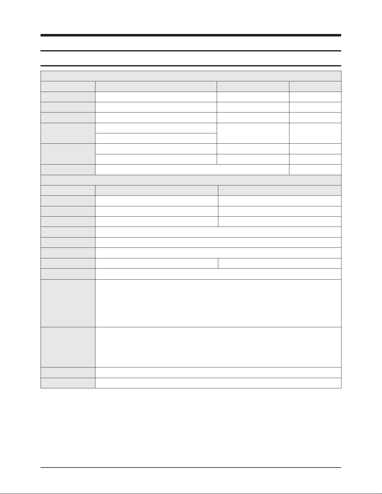
RF Tuner DNOS403MH261B(S) SEMCO
PDP Module Samsung SDI W2A 42"HD/50"HD SAMSUNG SDI
Power Input Voltage: AC 100~240V, 50/60Hz
Video
Scaler
SVP-UX68
Video Decoder
Sound
Sound AMP NTP3000 Neo Fidelity
Audio CODEC SGTV5810
Cabinet C9 Design
Specification
Model PS-42C96HD PS-50C96HD
Screen Size 42 Inches (16:9) 50 Inches (16:9)
Dimensions (WxHxD) 1055 x 759 x 316 mm (With Stand) 1231 x 848.5 x 316 mm (With Stand)
Weight 33.2 kg (With Stand) 44 kg (With Stand)
Voltage AC 100~240V, 50/60Hz
Colour System PAL, SECAM, NTSC4.43, NTSC 3.58
Sound System BG, DK, I, M
PC Resolution 1024 x 768 @ 85Hz 1365 x 768 @ 60Hz
ANTENNAinput AIR IN (75Ωunbalanced)
VIDEO input
SCART1, SCART2
AV (Side), S-VIDEO (Side)
COMPONENT IN (480i/P, 576i/P, 720P, 1080i)
PC IN (MINI D-SUB 15P)
HDMI1
HDMI2 (DVI IN)
AUDIO input
SCART1, SCART2
AV (Side), S-VIDEO (Side)
Component
PC
DVI
Audio Output AUDIO (L/R)
Speaker Output 10W + 10W
Page 30
Product Specification
2-2 Samsung Electronics
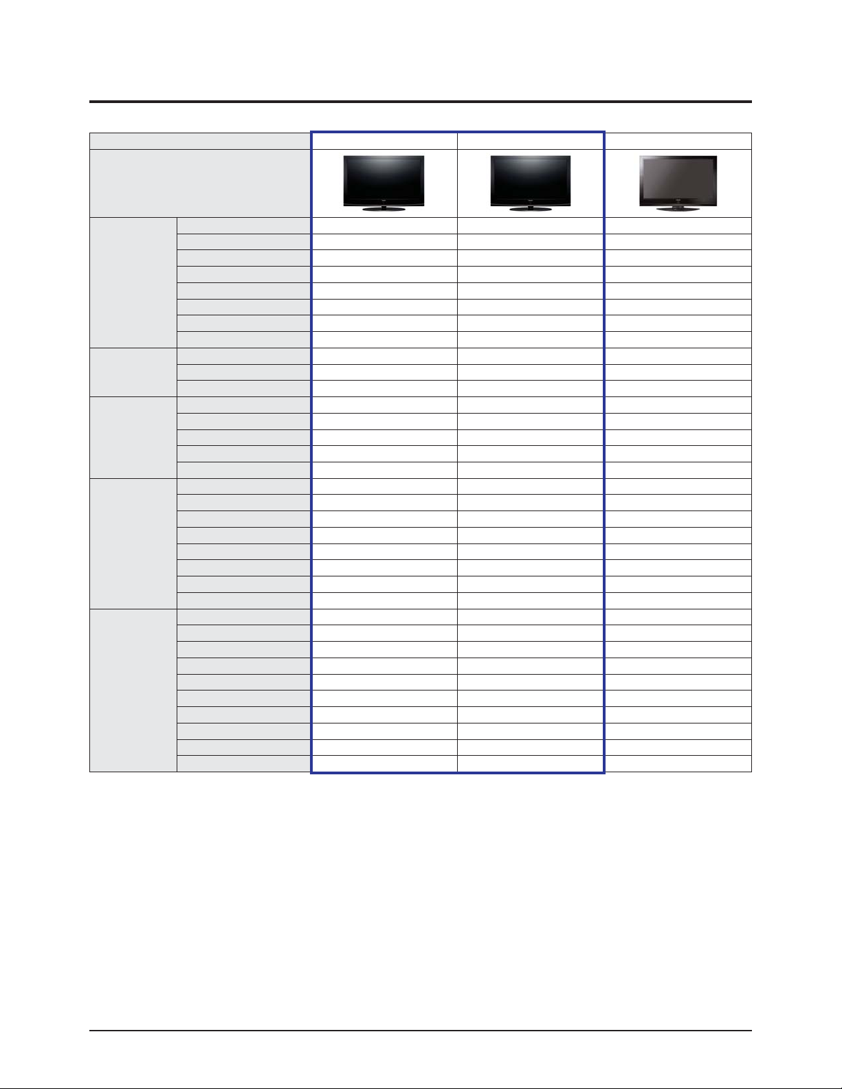
2-2 Specifications Analysis
Model PS-42C96HD (Lily-42HD) PS-50C96HD (Lily-50HD) PS-42P7HD (Alps-42HD)
Design
Basic
Display Type PDP TV PDPTV PDP TV
Built-In Tuner O O O
PC Resolution 1024 x 768 @ 85Hz 1365 x 768 @ 60Hz 1024 x 768 @75Hz
PDP Module W2A W2A V5.1
Screen Size 42 inches 50 inches 42 inches
Aspect Ratio 16 : 9 16 : 9 16 : 9
Dimensions (WxHxD) 1055 x 759 x 316 mm (With Stand) 1231 x 848.5 x 316 mm (With Stand) 1055 x 775 x 341 mm (With Stand)
Weight 33.2 kg (With stand) 44 kg (With stand) 40.4 kg (With Stand)
Picture
Brightness 1,500 Cd/m2 1,300 Cd/m2 1,100 Cd/m2
Contrast Ratio 10000:1 10000:1 10000:1
Image Enhacer FBE2X FBE2X FBE
Audio
Equalizer O O O
Auto Volume O O O
Surround Sound SRS TruSurround SRS TruSurround SRS TruSurround
Speaker Output 10 W + 10 W 10 W + 10 W 15 W + 15 W
Speaker 2CH 2.2CH (2Way) Included
Features
PIP O O O
Double Screen O O X
Caption X X X
Still Image O O O
My Color Control O O X
Color Weakness X X X
Energy Saving O O O
Screen Burn Protection O O O
Connections
Antenna 1 Input 1 Input 1 Input
CVBS 1AV(Side) 1AV(Side) 1AV(Rear)
S-Video O O 1 Input
Component(Y/PB/PR) 1 Input 1 Input 1 Input
PC(D-SUB) 1 Input 1 Input 1 Input
DVI O O O
HDMI 2 Input 2 Input 2 Input
Scart 2 Input 2 Input 2 Input
Optical O O O
Coaxial X X X
※○: application, X: non-application
※ For the power supply and power consumption, refer to the label attached to the product.
Page 31
Product Specification
Samsung Electronics 2-3
2-3 Accessories
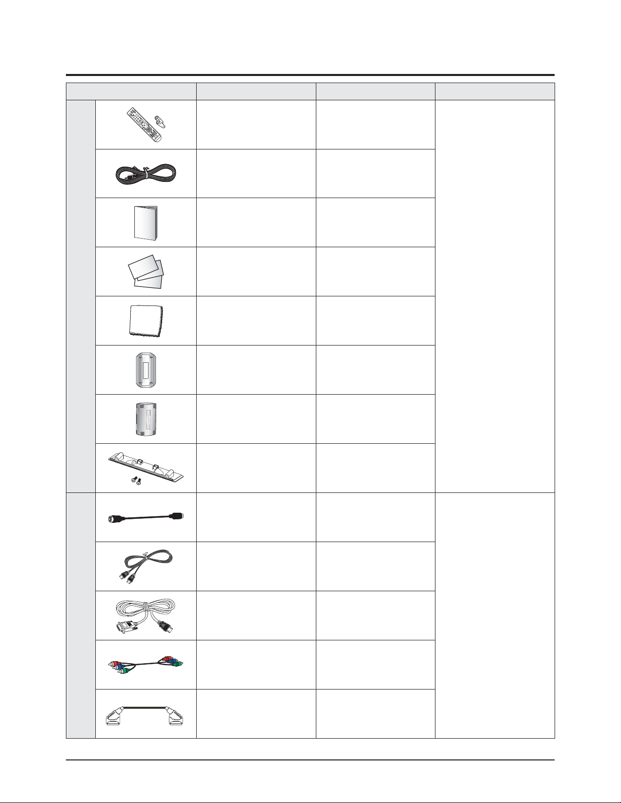
Accessories Item Item code Remark
SuppliedAccessories
Remote Control
Batteries
BN59-00611A
4301-000103
Samsung Service center
Power Cord 3903-000145
Owner's Instructions BN68-01171B
Warranty Card
Registration Card
Safety Guide Manual
BN68-00514C
AA68-03575A
AA68-03242E
Cloth-Clean BN63-01798A
Ferrite Core for
Earphone/Power Cord
3301-001110
Ferrite Core for
S-VIDEO/Power Cord
3301-001305
Cover-Bottom
Screws (2ea)
BN63-03055A
6003-001621
Accessories that canbe purchased
additionally
S-VIDEO Cable
1200mm
BN39-00149A
Electronics Store/
Internal shopping mall
HDMI Cable
3000mm
BN39-00641A
HDMI/DVI cable
3000mm
BN39-00643A
Component Cables (RCA)
1500mm
BN39-00279A
Scart Cable None
Page 32
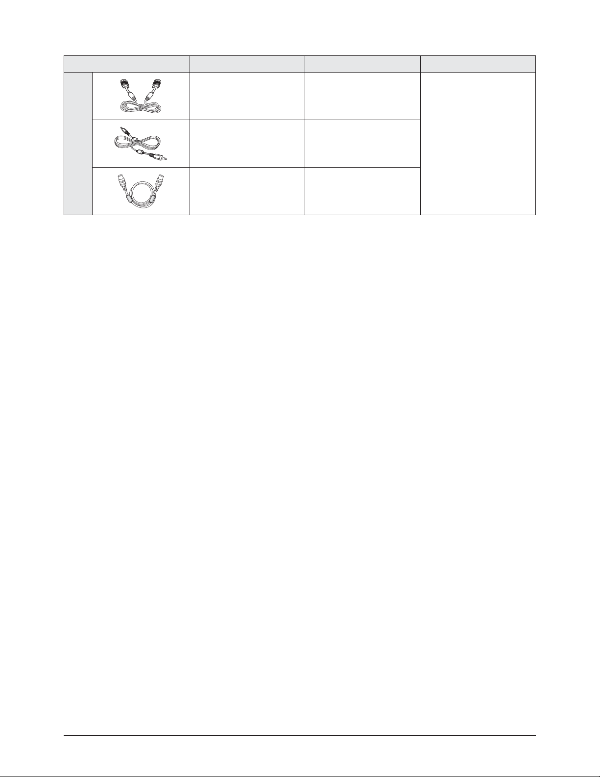
Product Specification
2-4 Samsung Electronics
Accessories Item Item code Remark
Accessories that canbe purchased
additionally
PC Cable
1830mm
BN39-00115A
Electronics Store/
Internal shopping mall
PC Audio Cable
2000mm
BN39-00061B
Antenna Cable
3000mm
BN39-00333A
Page 33
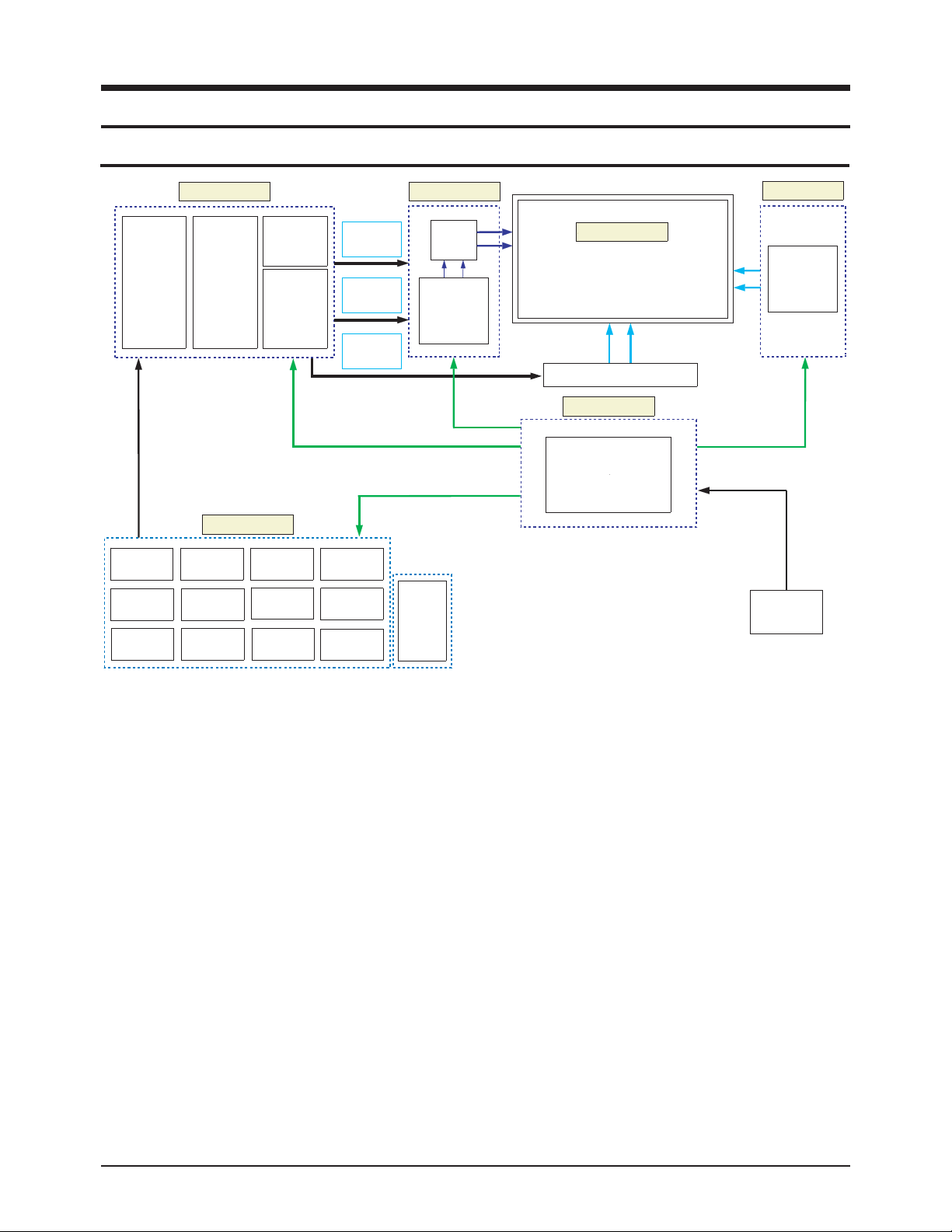
Schematic Diagram
Samsung Electronics 7-1
7. Schematic Diagram
7-1 Circuit Description
■ SMPS Board
The SMPS used for the PDP has been designed to be efficient, compact and lightweight. For VS and VAoutputs, a LLC converter
has been used. For the other outputs, a Flyback converter has been used.
■ LOGIC Board
The logic circuit consists of a Logic Main Board and an Address Buffer Board. The Logic Main Board decodes the video signal
encoded by the Video Board, outputs the ADDRESS data signal for each pattern and generates X and Y drive signals. The
Address Buffer Board buffers and transfers the ADDRESS data output signal using TCP IC.
- LVDS with built-in video signal processing (W/L, error diffusion, APC, FCR, etc.) applied and 1 ASIC chip.
- Outputs the address Drive IC control and data signals to the Buffer Board.
- Outputs the control signal for the X and Y Drive Boards.
- Monitors major drive voltages (Micom Circuit Block); detects if a surge voltage has been applied and protects the Drive Circuit.
- Temperature Adaptive Operating Mode (Low Temperature/Room Temperature/High Temperature); Discharge optimization for
each temperature level.
■ X-MAIN Board
Connects to the X terminal block, 1) provides maintaining voltage waveform (including ERC), and 2) maintains the Ve bias in the
Scan section.
■ Y-MAIN Board
Connects to the Y terminal block, 1) provides maintaining voltage waveform (including ERC), 2) provides Y Rising, Falling Ramp
waveforms, and 3) maintains the Vscan bias.
■ Address Buffer Board
It delivers the data signal and control signal to the TCP.
LVDS
Recever
Input
Data
Processor
LVDS
Trans
Image
Scaler
TMDS
Logic Board
Data
Controller
Main Board
Image
Enhancer
CPU
Decoder
A/D
Converter
DRAM
Driver
Timing
Controller
Deinterlacer
Video
Decoder
Video
S/W
Display
Data
Display
Timing
Scan
Timing
Audio
Processor
Speaker
Out
Micom
Y Main Board
Y-Pulse
Generator
Tune r
Row
Driver
PDP Panel
42” - 1024x768 Pixels
1024x768x3 Cells (R,G,B)
50” - 1365x768 Pixels
1365x768x3 Cells (R,G,B)
Address Buffer
SMPS Board
Main SMPS
X Main Board
X-Pulse
Generator
AC Power
Source
Page 34

7-2 Samsung Electronics
MEMO
Page 35
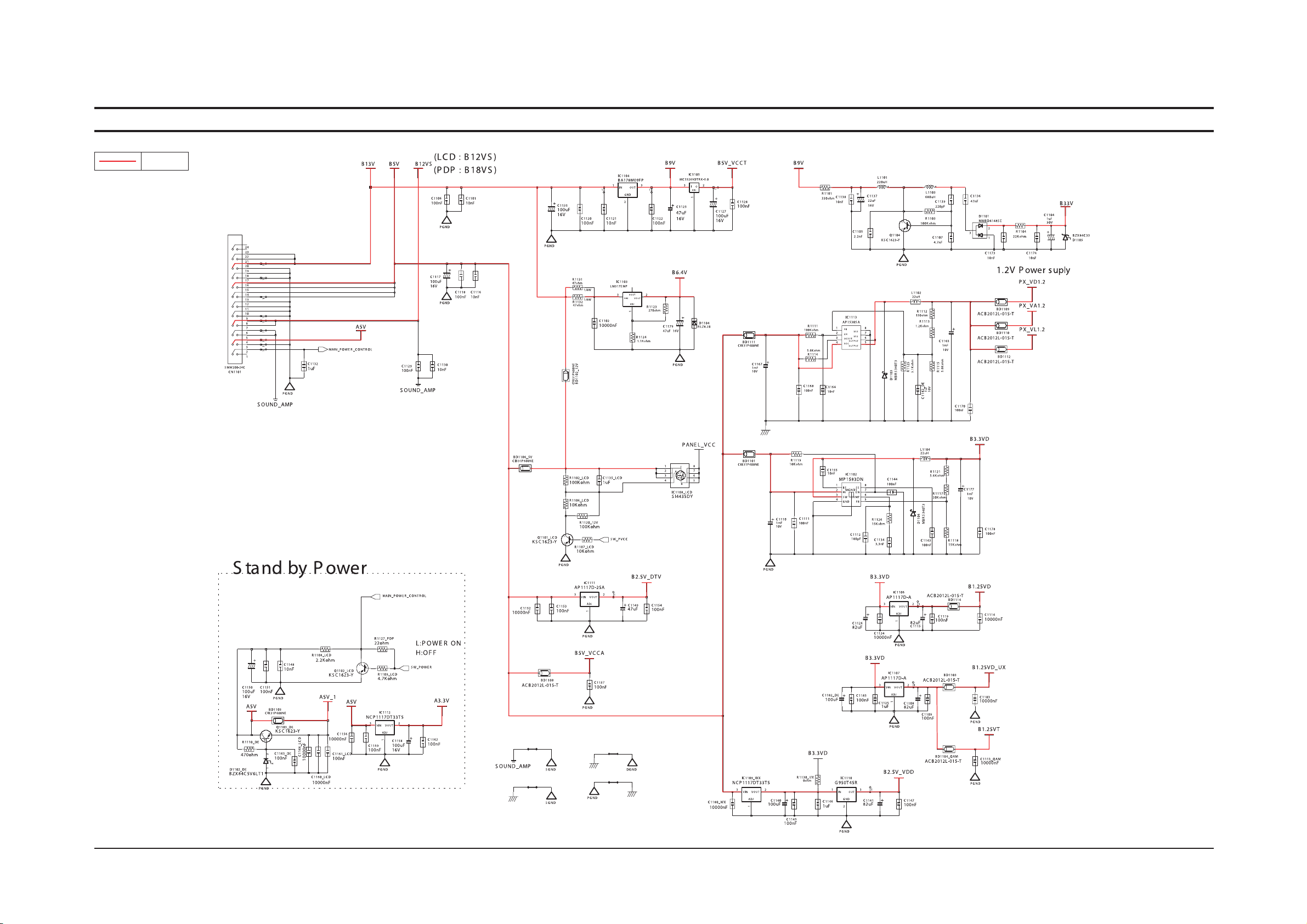
Samsung Electronics
Schematic Diagram
7-3
This Document can not be used without Samsung’s authorization.
7-2 Schematic Diagram
7-2-1 Power
Power
Page 36
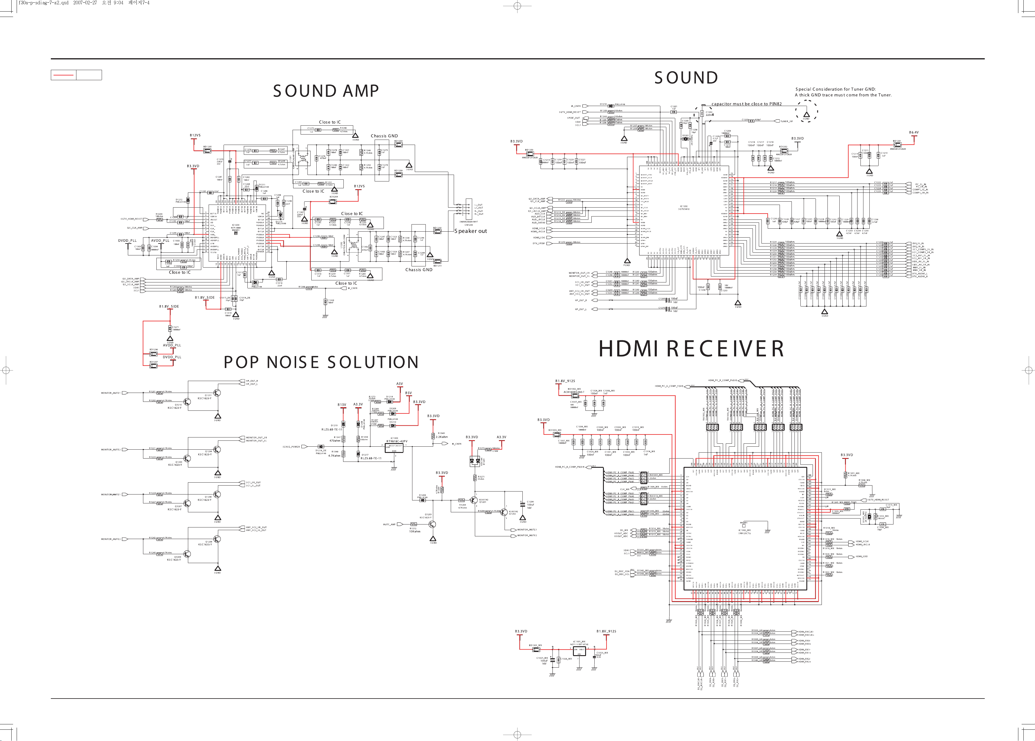
Samsung Electronics
Schematic Diagram
7-4
This Document can not be used without Samsung’s authorization.
7-2-2 Sound Processing
Power
Page 37
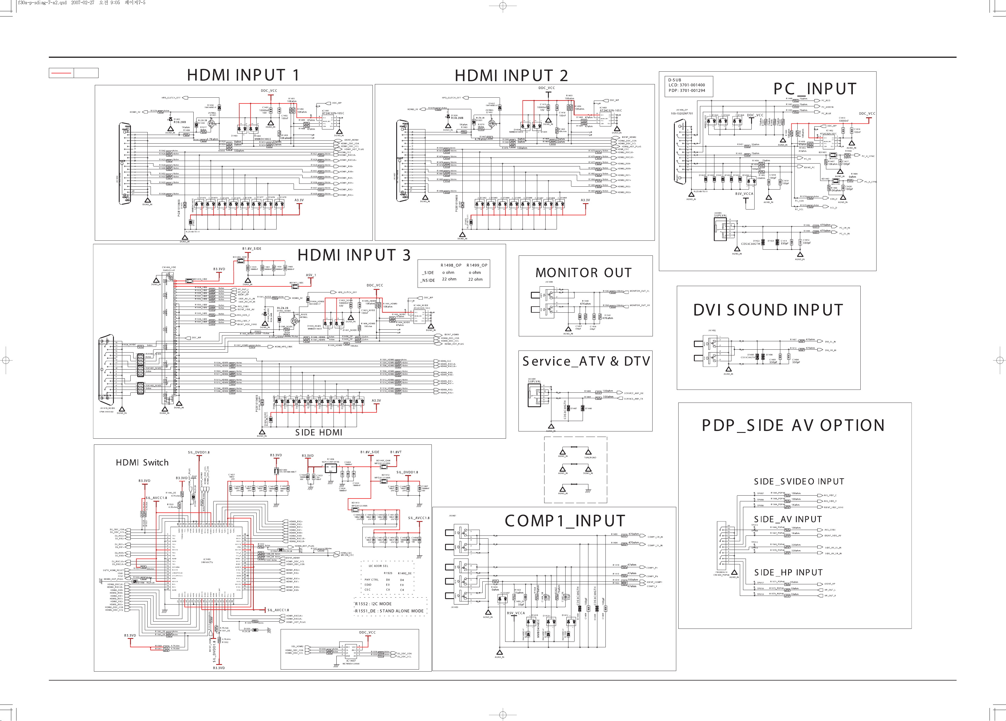
7-5
Schematic Diagram
Samsung Electronics
This Document can not be used without Samsung’s authorization.
7-2-3 Input & Output Jack I
Power
Page 38
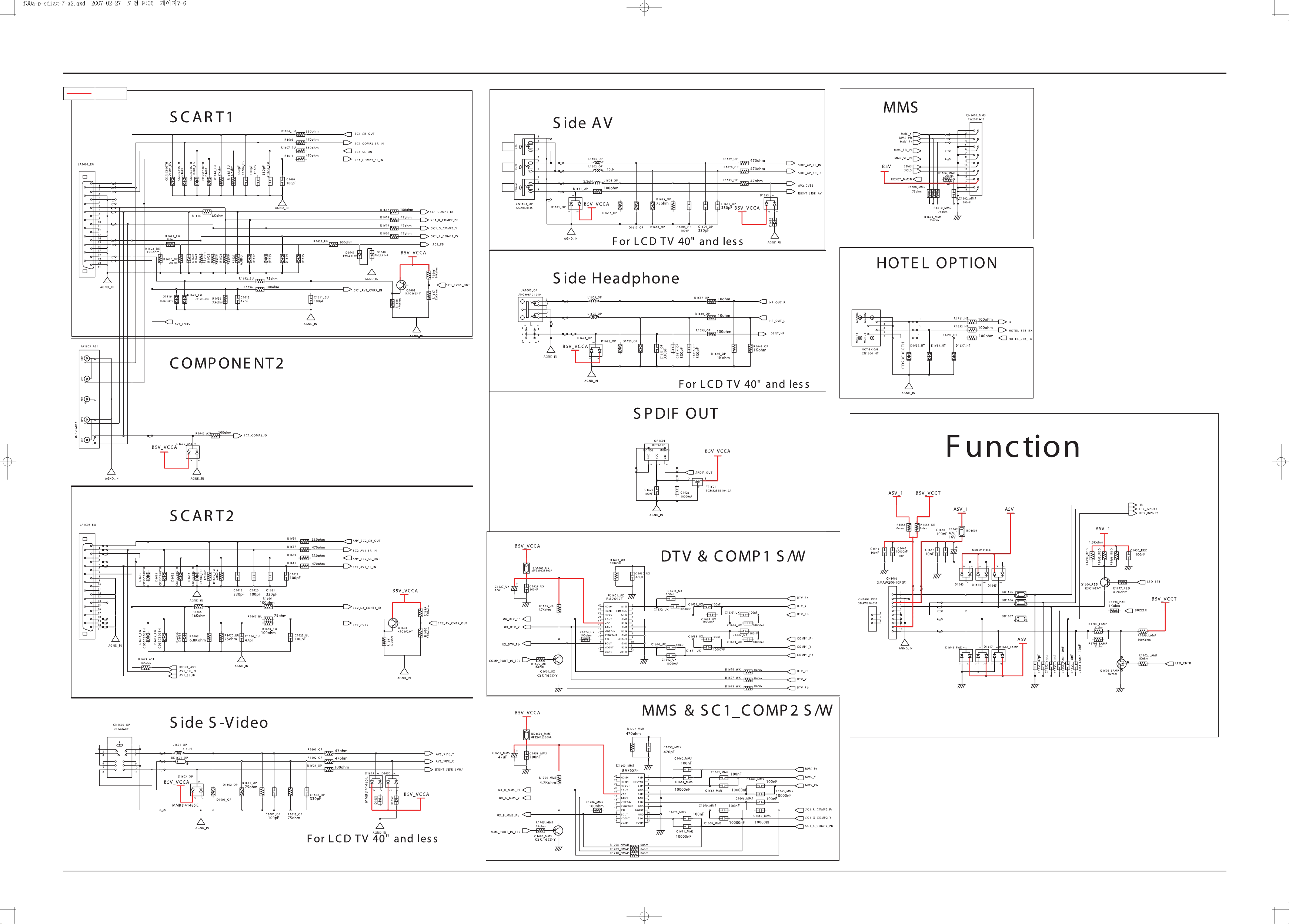
Samsung Electronics
Schematic Diagram
7-6
This Document can not be used without Samsung’s authorization.
7-2-4 Input & Output Jack II
Power
Page 39
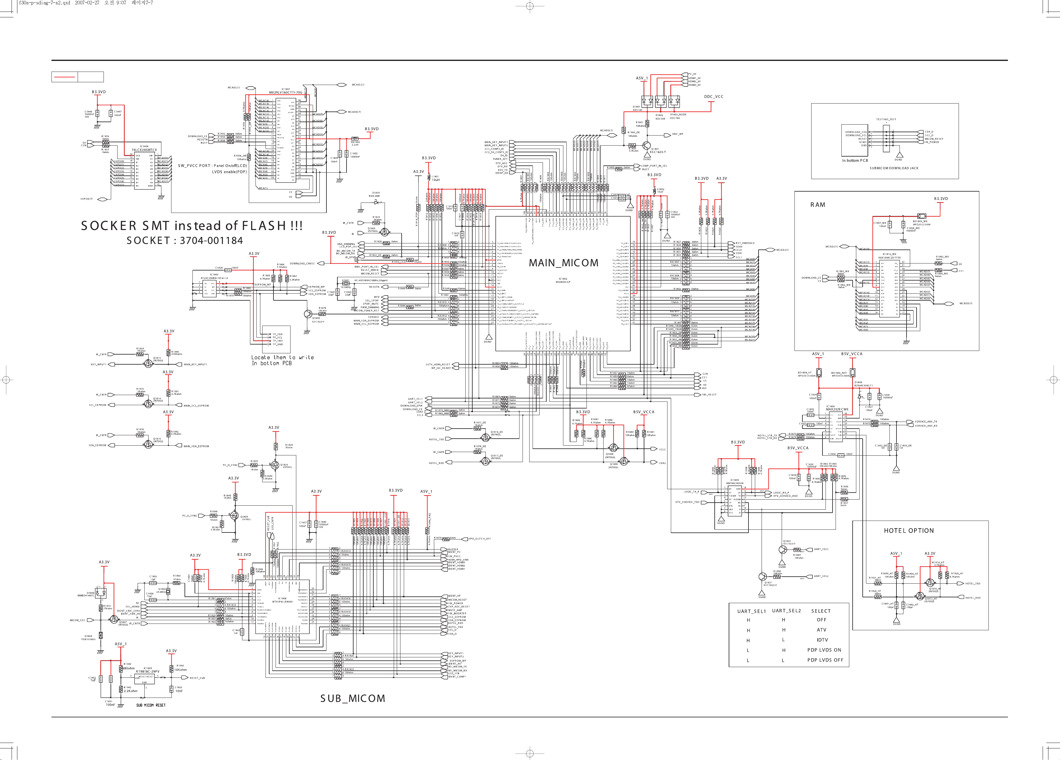
7-7
Schematic Diagram
Samsung Electronics
This Document can not be used without Samsung’s authorization.
7-2-5 MICOM
Power
Page 40
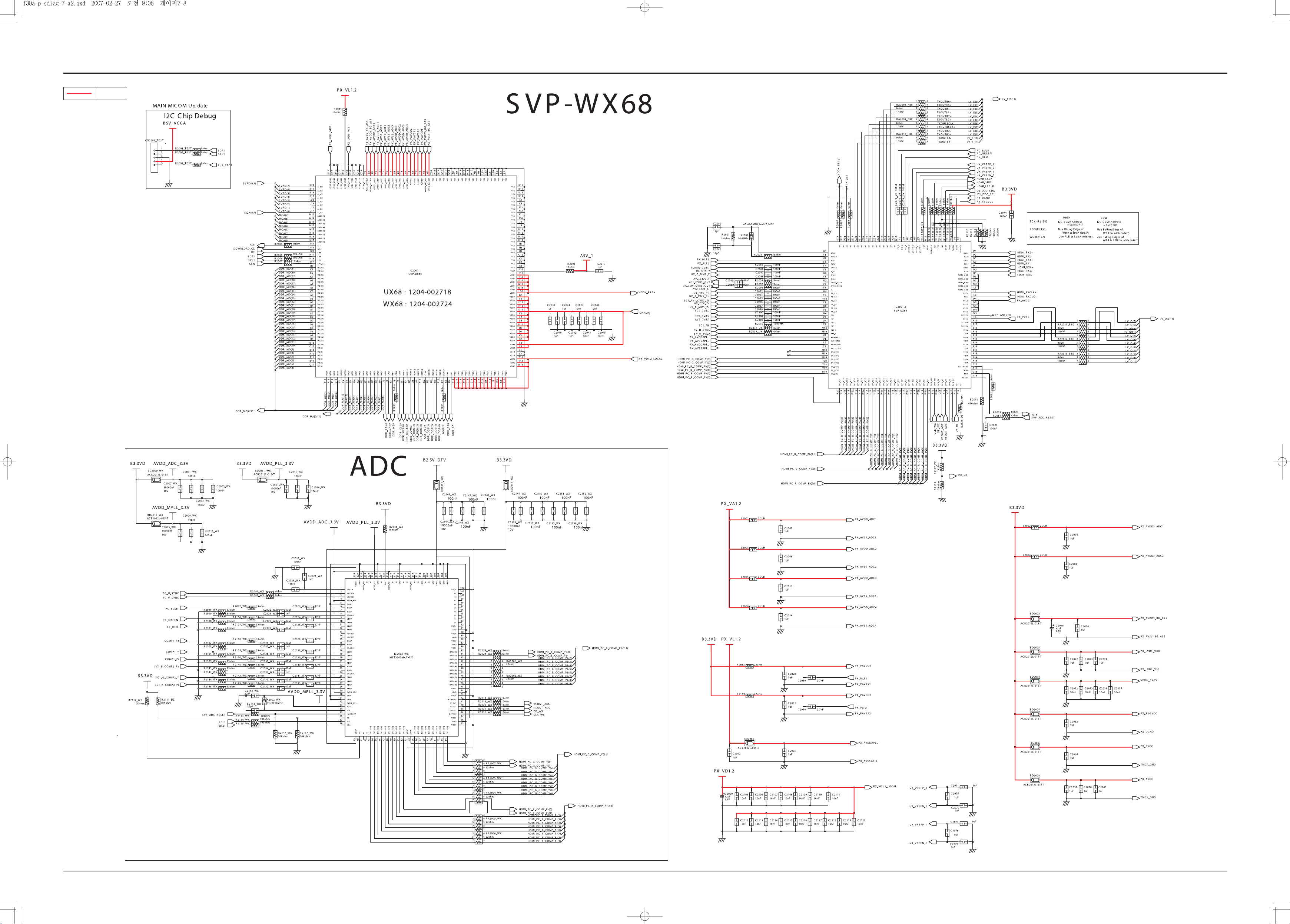
Samsung Electronics
Schematic Diagram
7-8
This Document can not be used without Samsung’s authorization.
7-2-6 SVP-UX (Scaler)
Power
Page 41
7-9
Schematic Diagram
Samsung Electronics
This Document can not be used without Samsung’s authorization.
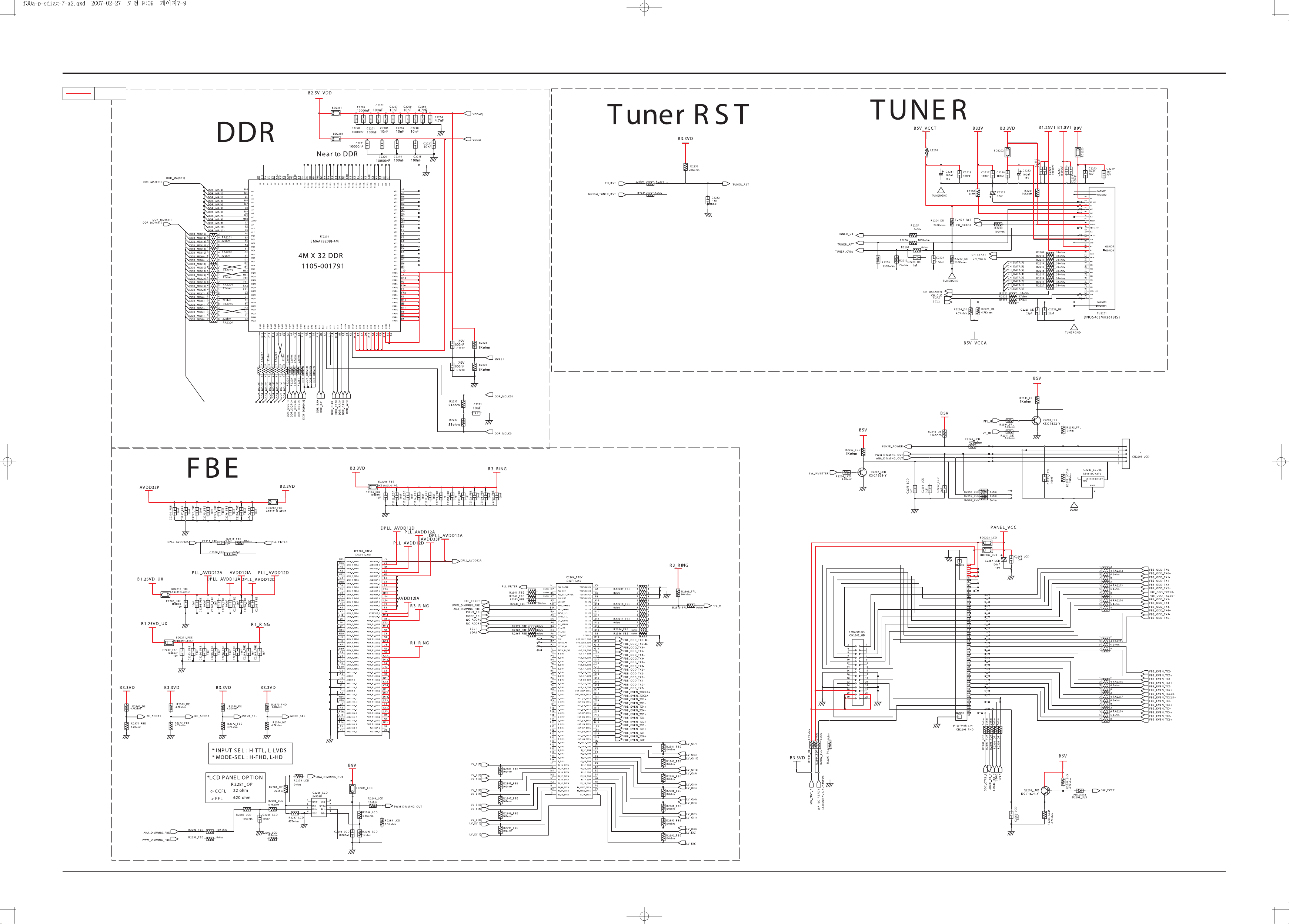
7-2-7 DDR & Tuner
Power
Page 42
Samsung Electronics
Schematic Diagram
7-10
This Document can not be used without Samsung’s authorization.
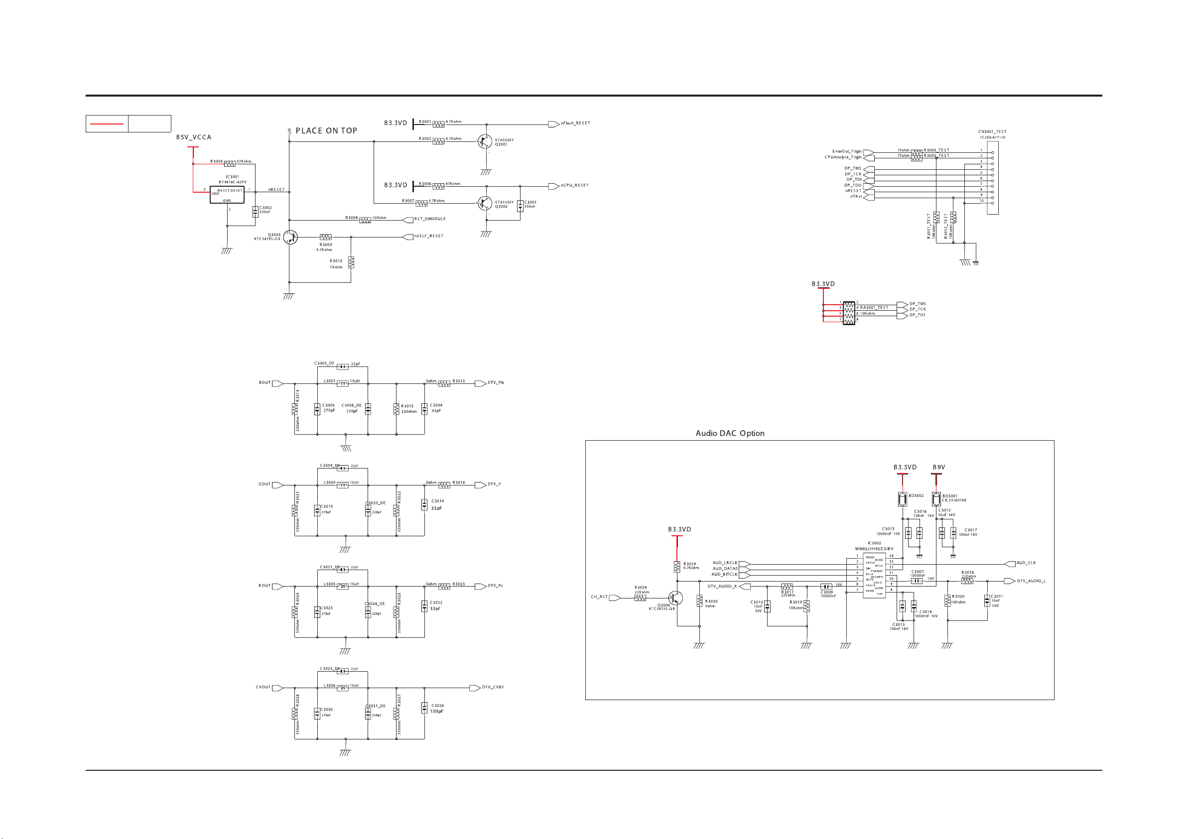
7-2-8 DTV Reset & AV out
Power
Page 43
Schematic Diagram
7-11 Samsung Electronics
This Document can not be used without Samsung’s authorization.
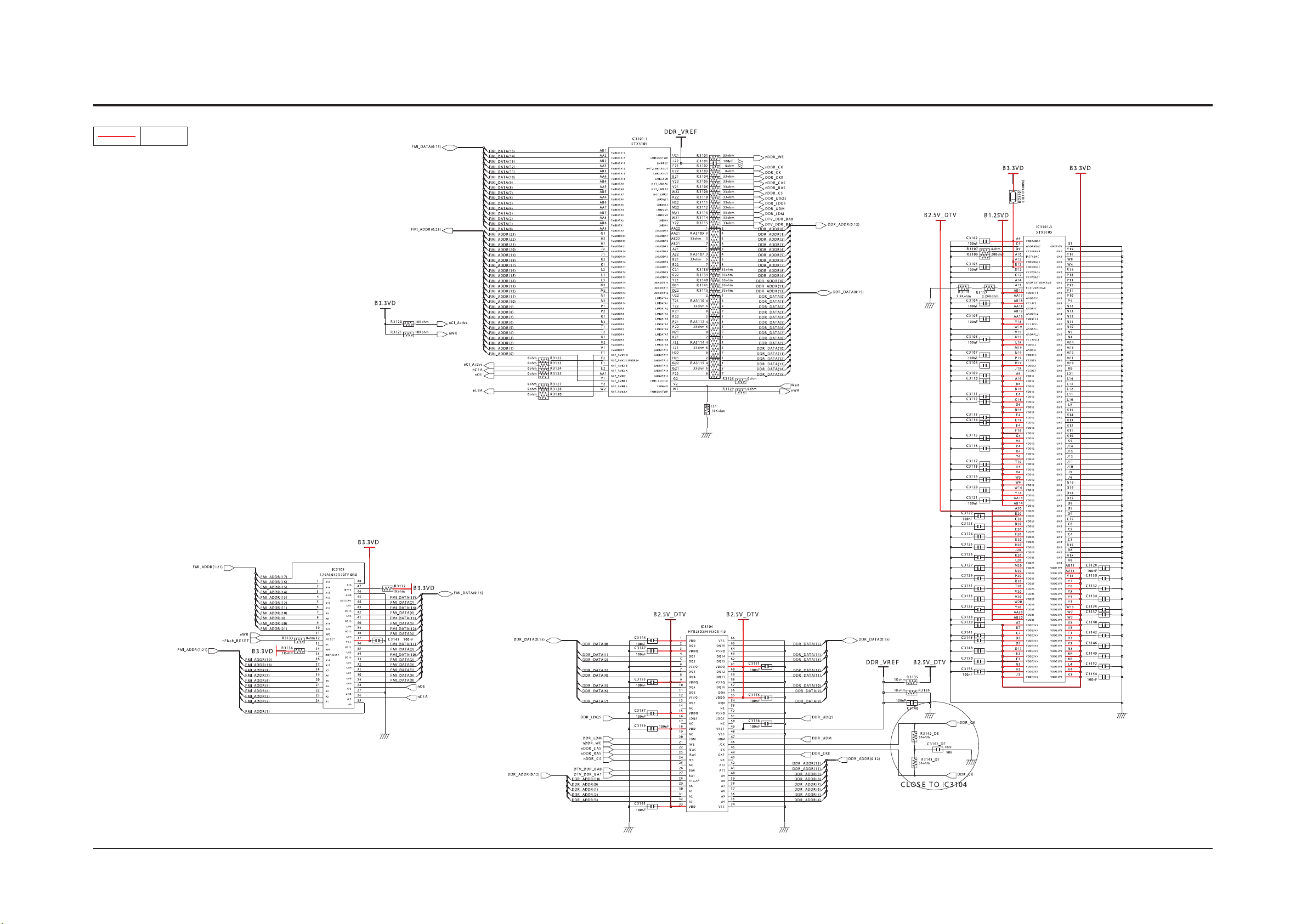
7-2-9 DTV Memory & STi5105
Power
Page 44
Samsung Electronics
Schematic Diagram
7-12
This Document can not be used without Samsung’s authorization.
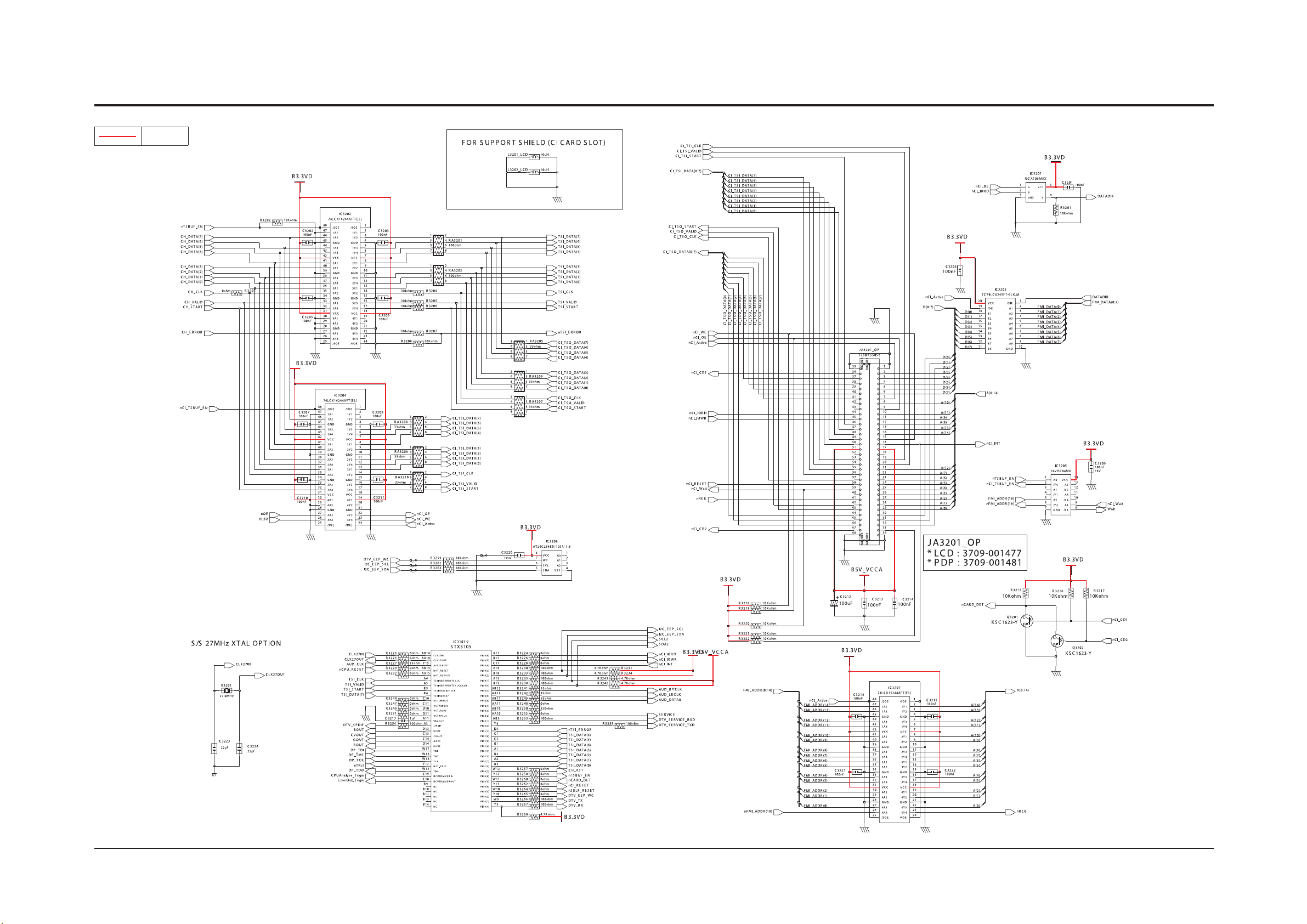
7-2-10 PCMCIA & STi5105
Power
Page 45

Troubleshooting
Samsung Electronics 4-1
4-1-1 First Checklist for Troubleshooting
1. Check the various cable connections first.
- Check to see if there is a burnt or damaged cable.
- Check to see if there is a disconnected or loose cable connection.
- Check to see if the cables are connected according to the connection diagram.
2. Check the power input to the Main Board.
3. Check the voltage in and out between the SMPS ↔ Main Board, between the SMPS ↔ X, Y Main Board, and between the
Logic Boards.
4. Troubleshooting
4-1 Troubleshooting
Page 46
Troubleshooting
4-2 Samsung Electronics
4-1-2 Checkpoints by Error Mode
■
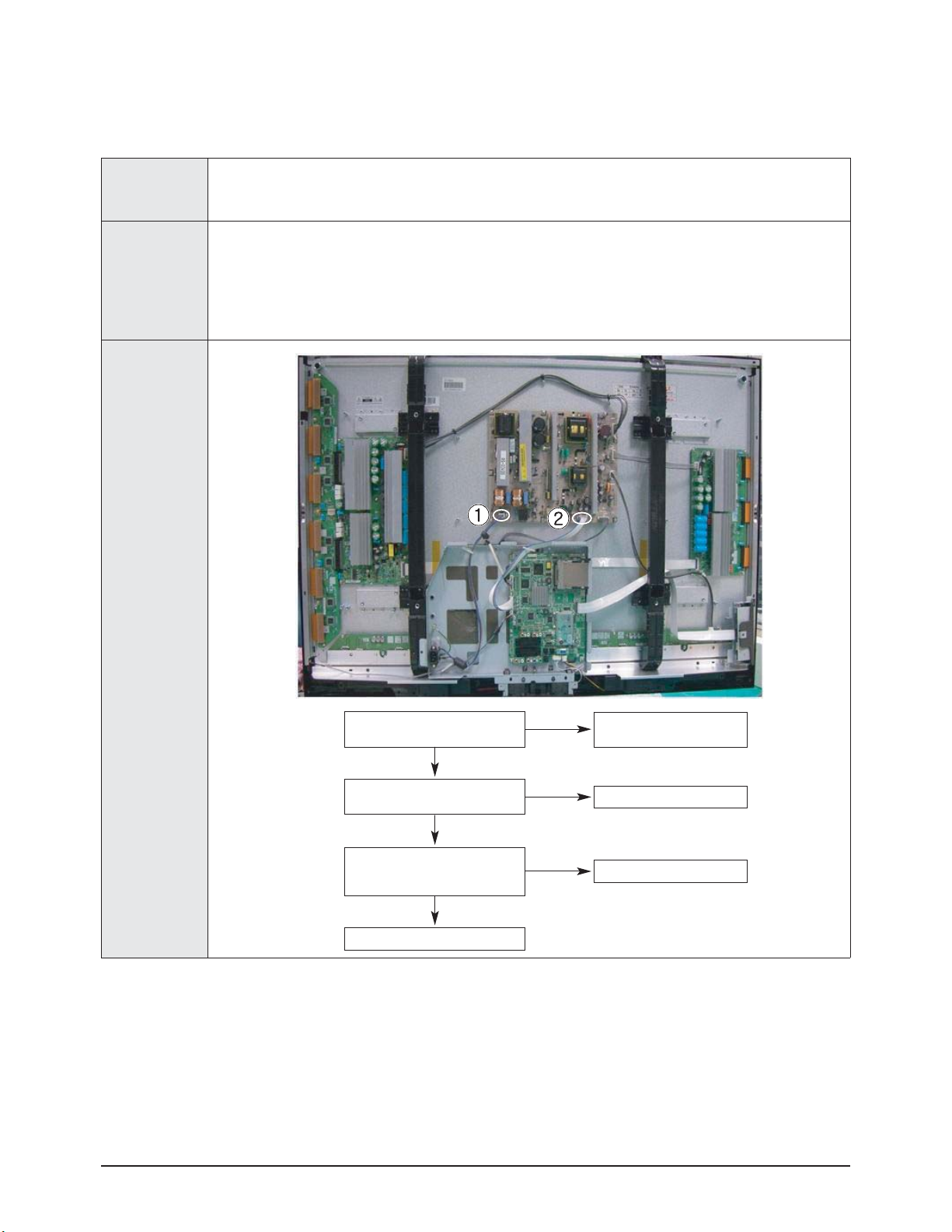
■
No Power
Symptom
Major Checklist
Troubleshooting
Procedures
Is the AC IN socket connector and
the SMPS CN800 connected?
Insert the AC in connector and the
SMPS CN800 connector
Is the Fuse (F801S) of the SMPS
Power Input Part blown?
Replace Fuse (F801S)
Replace the SMPS
SMPS CN801
Pin 3 : STB 5V
Pin 2 PS-ON : Check to see if it is 0V
Replace the Main Board
①
①
②
Yes
No
Yes
No
No
Yes
- The LEDs on the front panel do not work when connecting the power cord.
- The SMPS relay does not work when connecting the power cord.
- The unit appears to be dead.
The SMPS relay or the LEDs on the front panel does not work when connecting the power cord if the cables
are improperly connected or the Main Board or SMPS is not functioning. In this case, check the following:
- Check the internal cable connection.
- Check the fuses.
- Check the output voltage of the SMPS.
- Replace the Main Board.
Page 47
Troubleshooting
Samsung Electronics 4-3
■
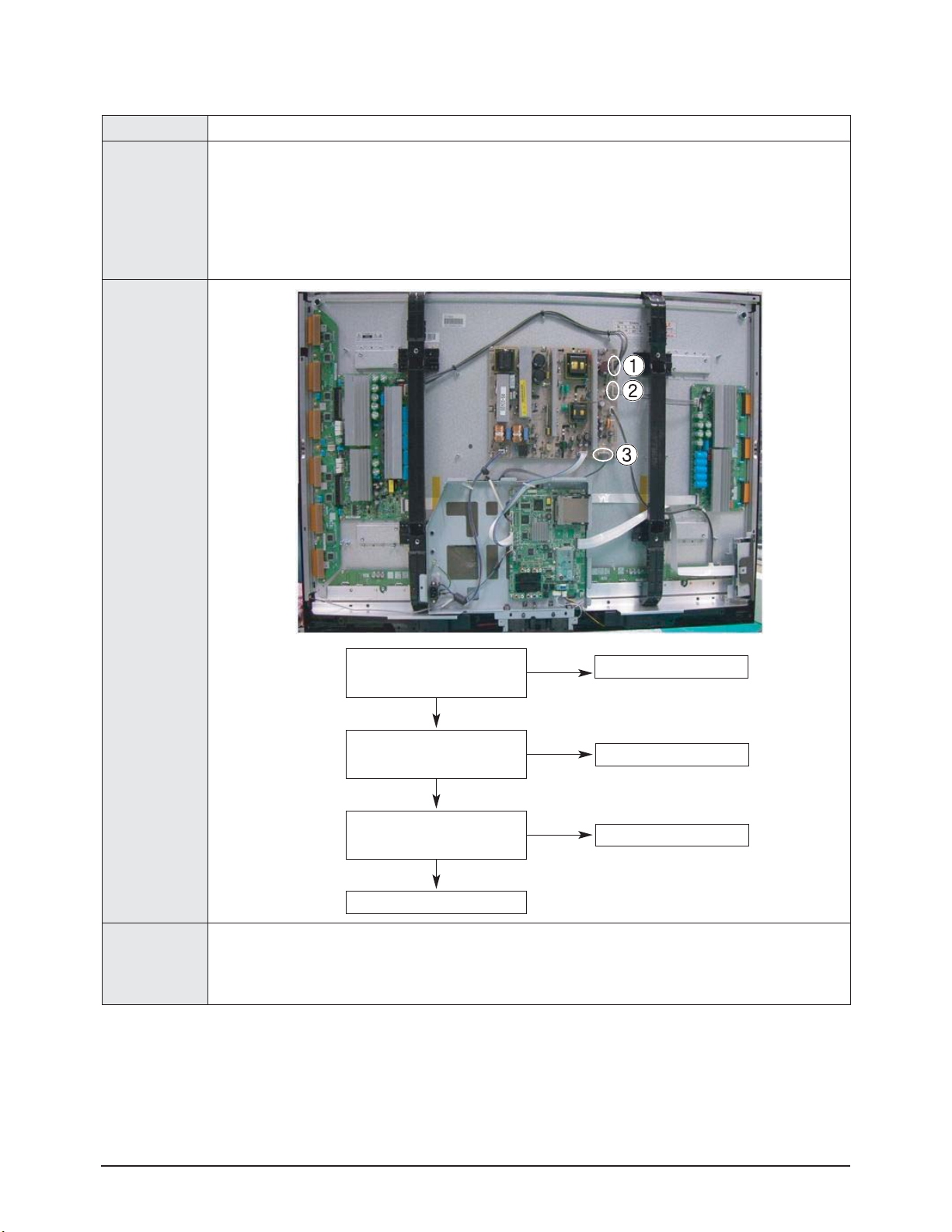
Symptom
Major Checklist
In general, the SMPS relay repeatedly turns on and off by the protection function due to a defect on a board
connected to the SMPS.
- Disconnect all cables from the SMPS, operate the SMPS alone and check if the SMPS works properly and if
each voltage output is correct.
- If the symptom continues even when SMPS is operated alone, replace the SMPS.
- If the symptom is not observed when operating the SMPS alone, find any defective assemblies by connecting
the cables one by one.
Troubleshooting
Procedures
Caution
WHEN SEPARATING AND CONNECTING THE CABLES SUCH AS CN810, CN809, CN808, CN807 OF THE
MAIN SMPS, CN4701 OF THE X MAIN BOARD, AND CN5707 OF THE Y MAIN BOARD, A SPARK MAY BE
GENERATED BY THE ELECTRIC CHARGE OF THE HIGH CAPACITY CAPACITOR. THEREFORE, WAIT
SOME TIME AFTER DISCONNECTING THE POWER CORD FROM THE UNIT.
Does the symptom continue when
connecting the power after removing
CN810 from the SMPS?
Replace the Y Main Board
Does the symptom continue when
connecting the power after removing
CN809 from the SMPS?
Replace the X Main Board
Replace the Logic Board
Does the symptom continue when
connecting the power after removing
CN807 from the SMPS?
Replace the SMPS
①
②
③
Yes
No
No
No
Yes
Yes
■
When the unit is repeatedly turning on and off
- The SMPS relay is repeatedly turning on and off.
Page 48
Troubleshooting
4-4 Samsung Electronics
■
■
No Picture (When audio is normal)
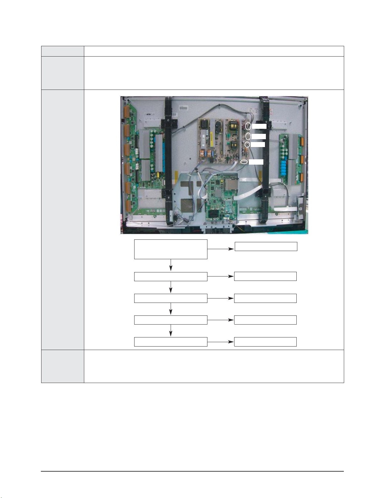
Symptom - Audio is normal but no picture is displayed on the screen.
Major Checklist
- This may happen when the Main Board is functioning but the X, Y Main Board, Logic Board, or Y Buffer
Boards are not.
- The output voltage of the Main SMPS.
- This may happen when the LVDS cable connecting the Main Board and the Logic Board is disconnected.
Troubleshooting
Procedures
Caution
WHEN SEPARATING AND CONNECTING THE CABLES SUCH AS CN810, CN809, CN808, CN807 OF THE
MAIN SMPS, CN4701 OF THE X MAIN BOARD, AND CN5707 OF THE Y MAIN BOARD, A SPARK MAY BE
GENERATED BY THE ELECTRIC CHARGE OF THE HIGH CAPACITY CAPACITOR. THEREFORE, WAIT
SOME TIME AFTER DISCONNECTING THE POWER CORD FROM THE UNIT.
Are the Vs and Va voltages normal after
removing all cables from the SMPS?
(CN810, CN809, CN808, CN807)
Replace the SMPS
Yes
No
Did problem improve?
Did problem improve?
Did problem improve?
Did problem improve?
Replace the Y Main Board
Replace the X Main Board
Replace the Logic Board
Replace the Y Scan Board
No
No
No
No
Yes
Yes
Yes
CN810
CN809
CN808
CN807
Page 49
Troubleshooting
Samsung Electronics 4-5
■■
No Sound
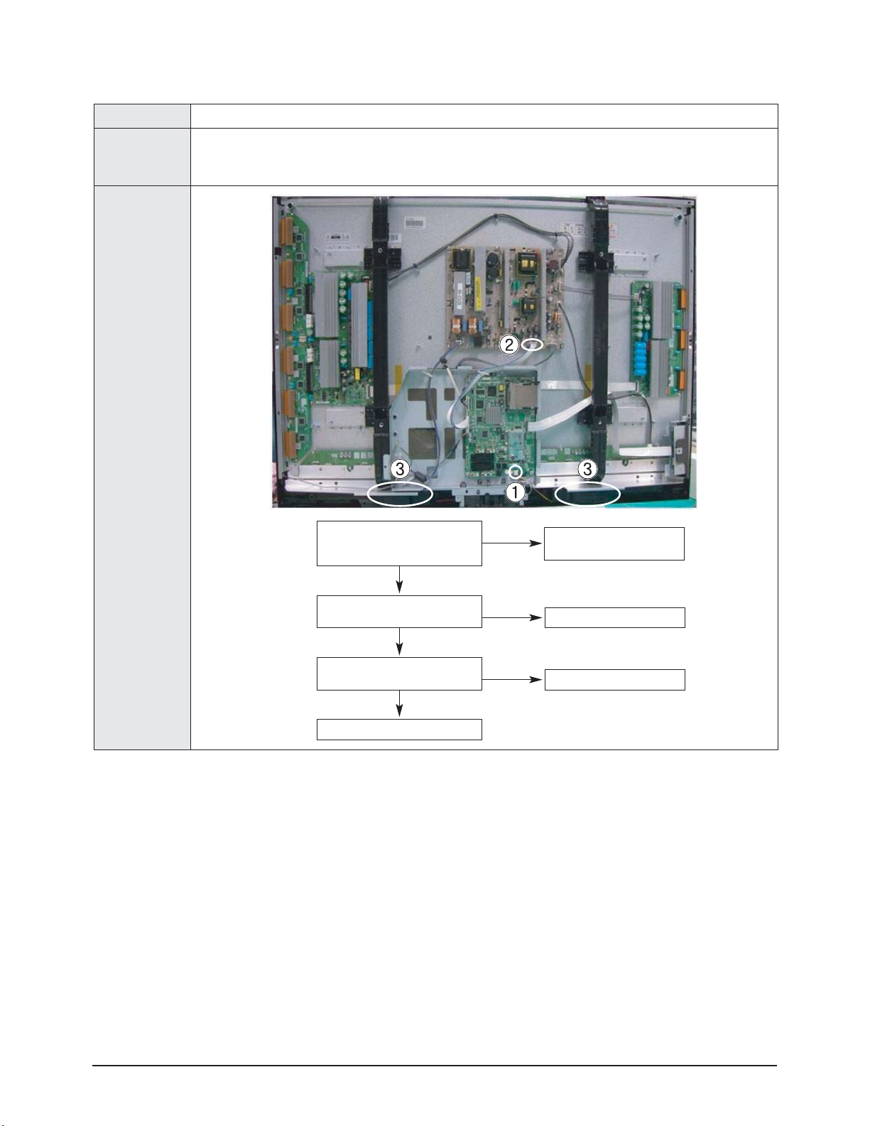
Symptom - Video is normal but there is no sound.
Major Checklist
- When the speaker connectors are disconnected or damaged.
- When the sound processing part of the Main Board is not functioning.
- Speaker defect.
Troubleshooting
Procedures
Is the cable connection between the
Main Board and the speaker
properly connected?
Connect the cable properly or
replace the cable, if necessary.
Is the output voltage of SMPS normal?
(CN801 #13)
Replace the SMPS
Replace the Main Board
Is the speaker output terminal
of the Main Board normal?
Replace the Speaker
①
②
③
Yes
No
No
No
Yes
Yes
Page 50
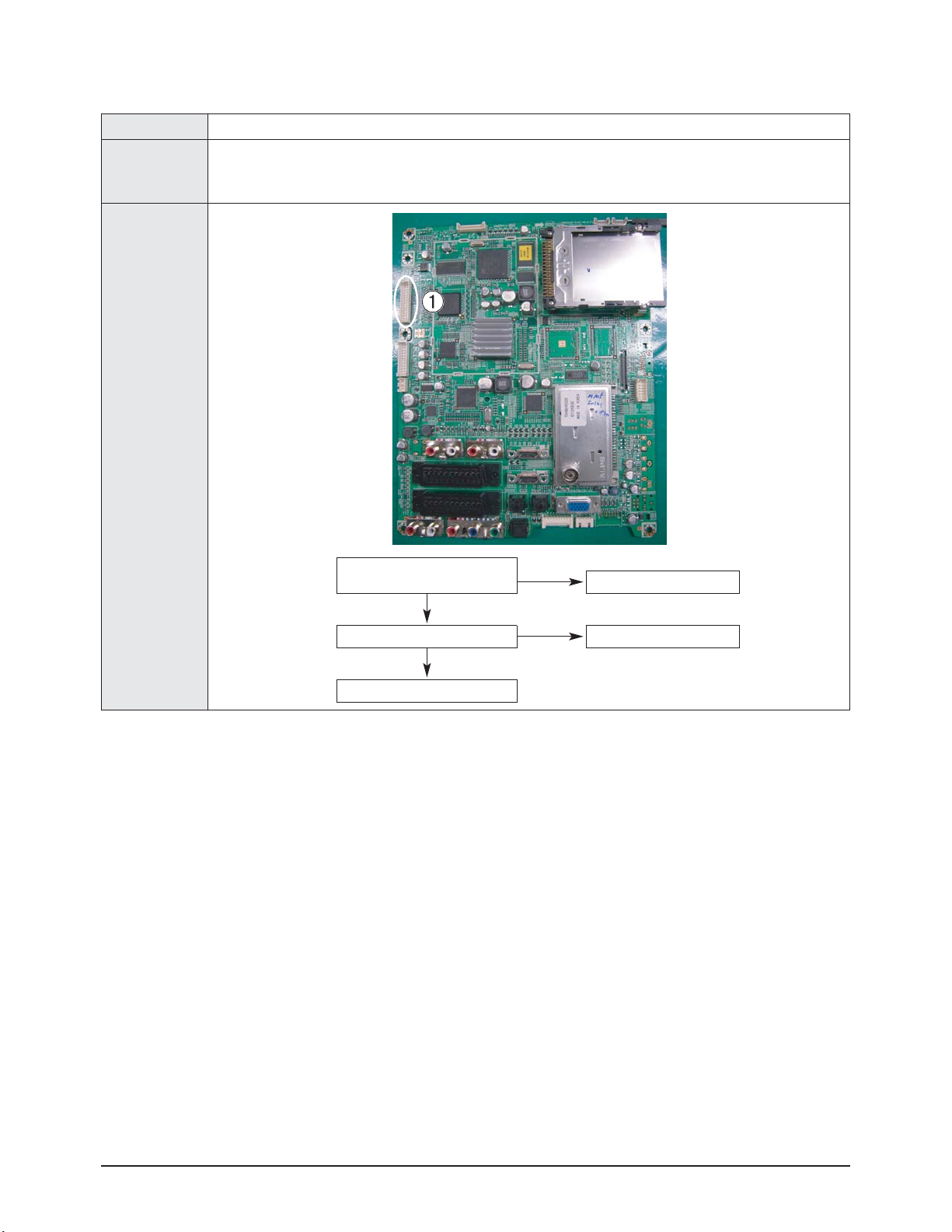
Troubleshooting
4-6 Samsung Electronics
■
■
No Video
Symptom - A normal/cable network analog broadcast screen is blank or abnormal but OSD is OK.
Major Checklist
- Check the antenna connection settings (Air: NTSC / ATSC, Cable: NTSC)
- Check the CVBS cable connection.
- Check the power input of the Main board.
Troubleshooting
Procedures
Is the antenna connection setting
properly configured?
Configure properly
Replace the SMPS
Check CN1101 pin2 for +33V
Replace the Main Board
①
No
No
Yes
Yes
Page 51
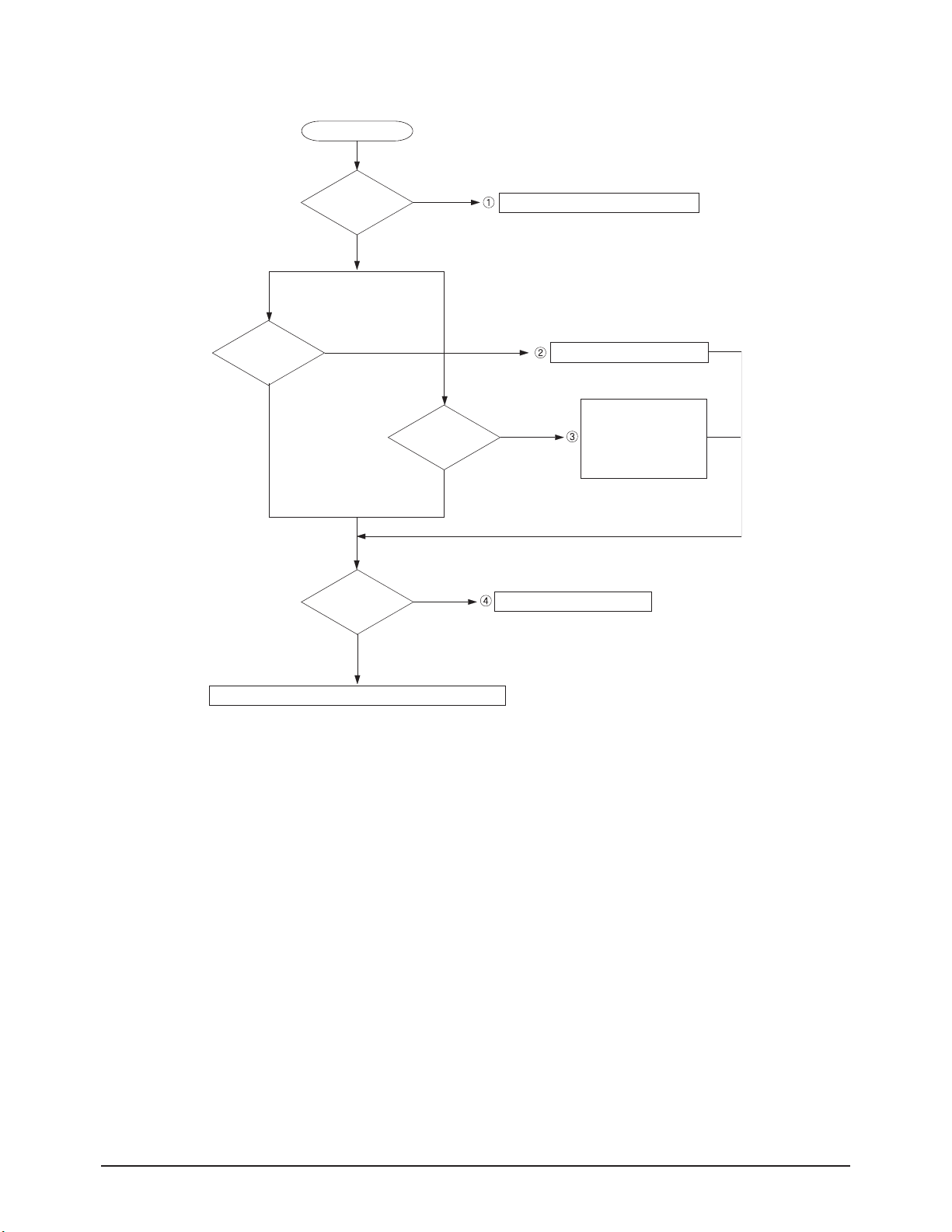
Troubleshooting
Samsung Electronics 4-7
■
SMPS Troubleshooting
Power ON
VA
STD_5V
Normal PS-ON
Abnormal
Normal VS-ON
VS
Abnormal
Multi
Abnormal
Check the ICB802, DB864, FB801, F801S
Check the SUB2, QX801,QX802
Check the
Abnormal
Check the SUB1,QS801,QS802
5.3V : ICX808, QX806
12V : ICX803
VG : ICX805
18Vamp : ICX804
Normal
Check the Other board (Image Board or Driver Board) or Cable.
Page 52
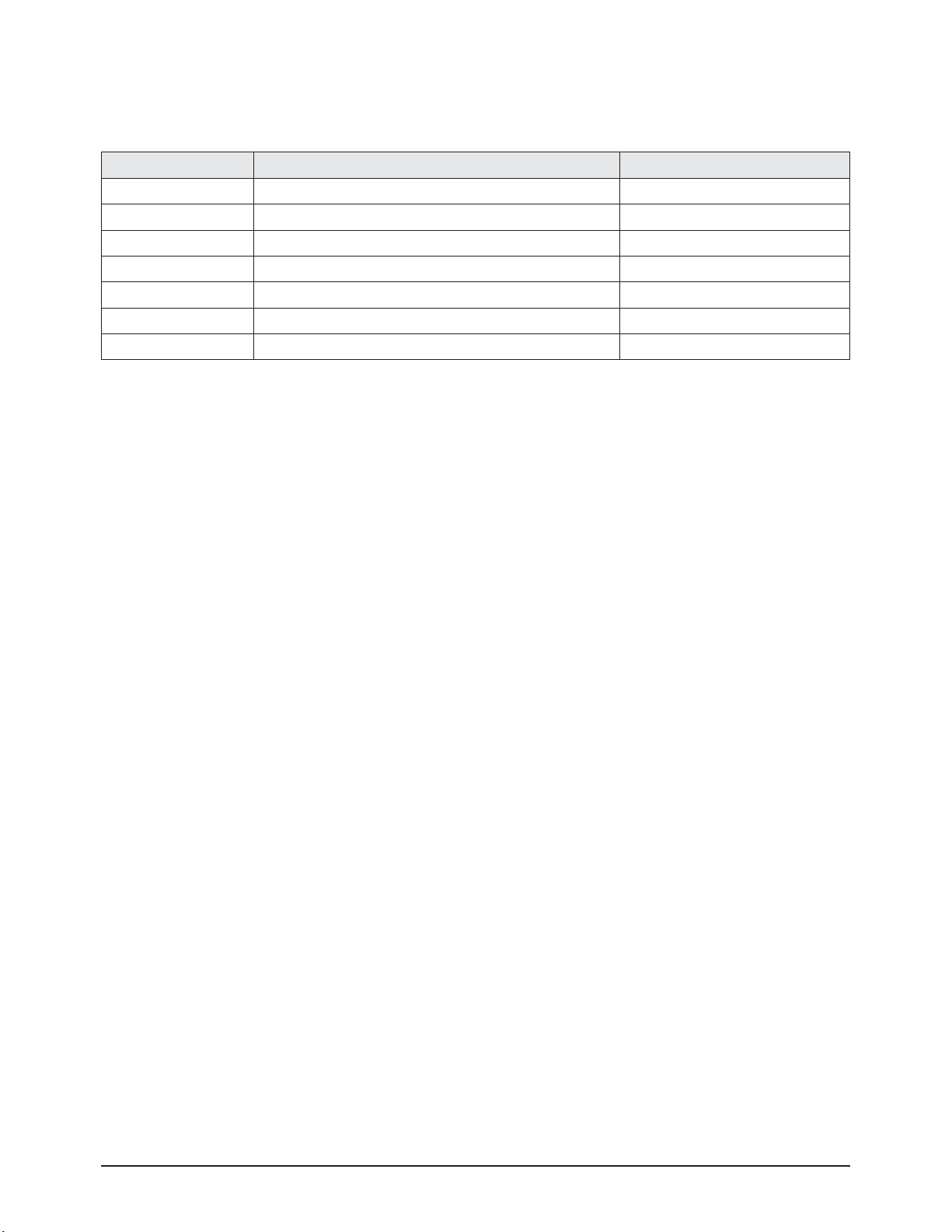
Troubleshooting
4-8 Samsung Electronics
Condition Name Description Related Board
No Voltage Output Operating Voltage don't exist PSU
No Display Operating Voltage exist, but an Image doesn't exist on screen Y-MAIN, X-MAIN, Logic Main, Cable
Abnormal Display Abnormal Image (not open or short) is no screen Y-MAIN, X-MAIN, Logic Main
Sustain Open Some horizontal lines don't exist on screen Scan Buffer, FPC of X/Y
Sustain Short Some horizontal lines appear to be linked on screen Scan Buffer, FPC of X/Y
Address Open Some vertical lines don't exist on screen Logic Main, Logic Buffer, TCP
Address Short Some vertical lines appear to be linked on screen Logic Main, Logic Buffer, TCP
■
■
Drive Board Troubleshooting
1) Troubleshooting Summary
Page 53
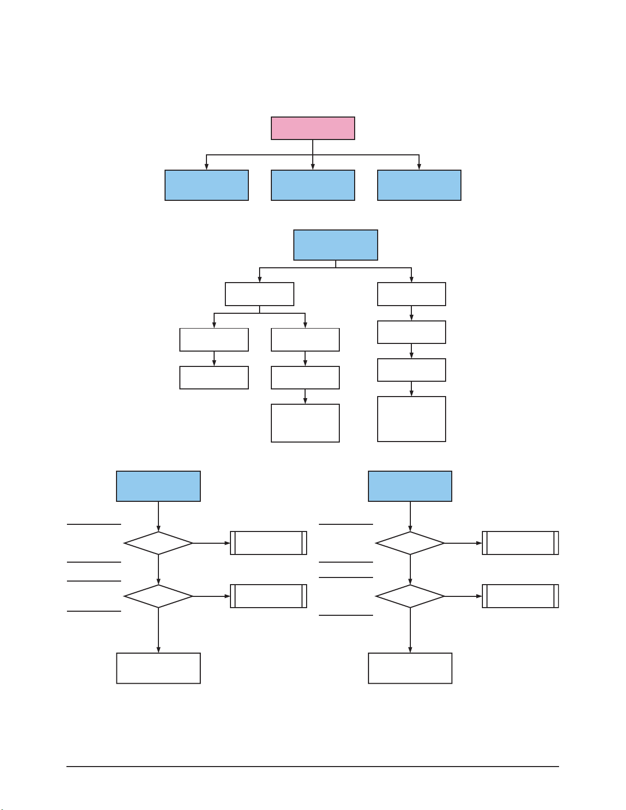
Troubleshooting
Samsung Electronics 4-9
2) Troubleshooting Procedure in Abnormal Conditions
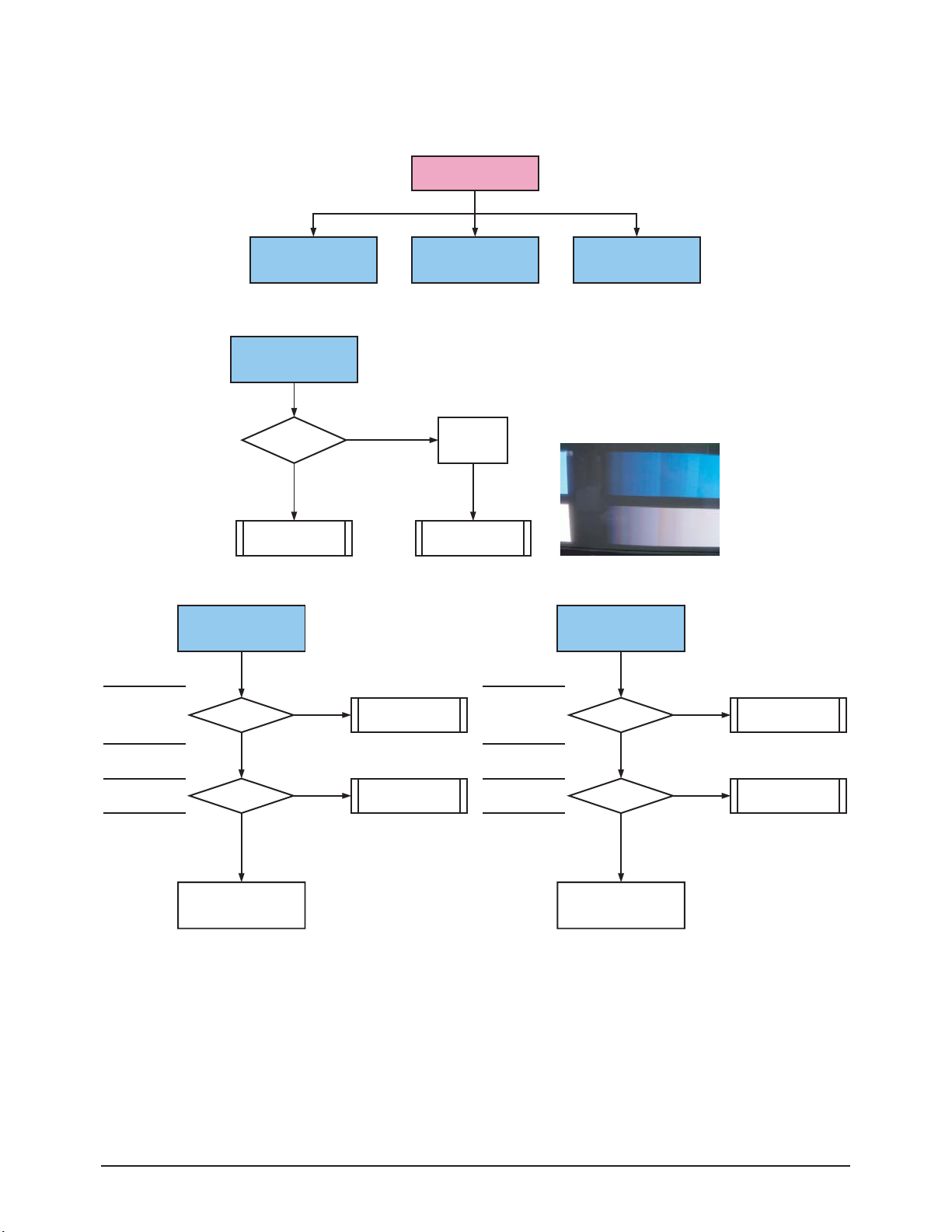
① No Display
▶ No Display is related with Y-MAIN, X-MAIN, Logic Main and so on.
This page shows you how to check the boards, and the following pages show you how to find the defective board.
No Display
[ Logic Main ]
LED Blinks
Check the LED
YES NO
Check if internal is
Check if any address
data output is detected
Default Black
[ Y-MAIN ]
Check necessary points
[ Logic Main ]
Check if power is supplied
YES NO
operation
MICOM operation
Check the ASIC
Control Signal output
Check if the data
and control signals
between DDR & ASIC
( 5V, 3.3V )
Check the
are normal
[ X-MAIN ]
Check necessary points
Check the
power connectivity
Check the FUSE
Check the
input voltage
If the input voltage is
abnormal, replace the
PSU and check it
again as this indicates
a PSU output error
[ X-MAIN ]
Check several points
FUSE
OK
FET/
DIODE
OK
X-MAIN
Normal State
OPEN
Replace the Board
SHORT
Replace the Board
F5001 for VDD
F5002 for Vs
F5004 for VCC
F5005 for OUT_L
Q5009~Q5021
D5005, D5007
D5008
[ Y-MAIN ]
Check several points
FUSE
OK
FET/
DIODE
OK
Y-MAIN
Normal State
OPEN
SHORT
Replace the Board
Replace the Board
F4001 for VCC
F4002 for Vs
F4004 for VDD
F4005 for Ve
Q4002~Q4003
Q4011~Q4016
D4004
D4006~D4008
Page 54
Troubleshooting
4-10 Samsung Electronics
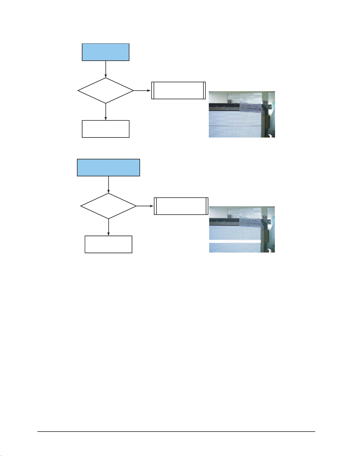
② Abnormal Display(Abnormal Image is on Screen.(except abnormality in Sustain or Address))
▶ Abnormal Display is related with Y-MAIN, X-MAIN, Logic Main and so on.
This page shows you how to check the boards, and the following pages show you how to find the defective board.
Abnormal
Display
F5001 for VDD
F5002 for Vs
F5004 for VCC
F5005 for OUT_L
[ Logic Main ]
LED Blinks
( action of Vsync )
YES
Replace the Board
[ Y-MAIN ]
Check several points
FUSE
OK
[ Logic Main ]
Observation of
abnormal display
Regular
abnormal
pattern
OPEN
Check necessary points
NO
Replace the Board
[ Y-MAIN ]
Logic Main
Normal State
Replace Panel
F4001 for VCC
F4002 for Vs
F4004 for VDD
F4005 for Ve
[ X-MAIN ]
Check necessary points
[ X-MAIN ]
Check several points
FUSE
OK
OPEN
Replace the Board
Q5009~Q5021
FET
OK
Y-MAIN
Normal State
SHORT
Replace the Board
Q4002~Q4003
Q4011~Q4016
FET
OK
X-MAIN
Normal State
SHORT
Replace the Board
Page 55
Troubleshooting
Samsung Electronics 4-11
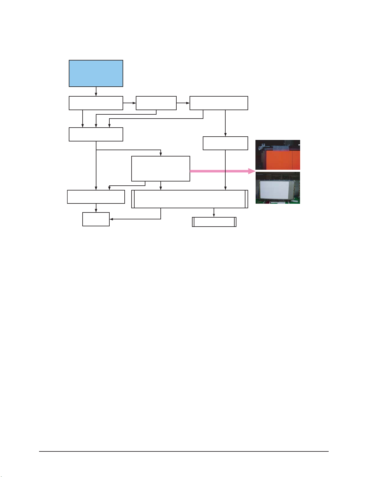
③ Sustain Open (some horizontal lines don't exist on screen)
④ Sustain Short (some horizontal lines appear to be linked on Video)
[ Y-FPC ]
Sustain Open
After Changing Y-buffer,
recheck the status
OK
Done
(Defect is from Y-buffer)
NG
Replace the Panel
There is a defect on the FPC
[ Y-FPC ]
(Discharging in unwanted Scan line)
Sustain Short
After Changing Y-buffer,
recheck the status
OK
Done
(Defect is from Y-buffer)
NG
Replace the Panel
There is a defect on the FPC
Page 56
Troubleshooting
4-12 Samsung Electronics
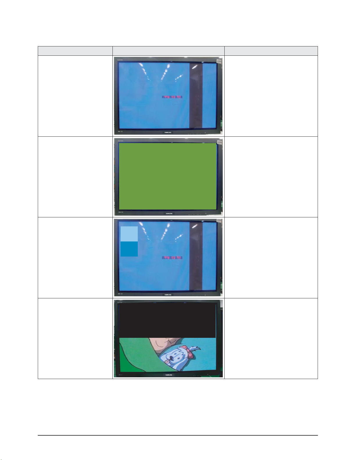
⑤ Address Open, Short
▶ Address Open and Short is related with Logic Main, Logic Buffer, FFC, TCP film and so on.
This page shows you how to check the boards, and the following pages show you how to find the defective board.
[ Logic Main ]
Address Open/Short
Check the LED operation
LED2011 : blink
LED2010 : on
Check if the internal mode
screen is normal
OK
Reload the data onto the
MICOM and recheck it
Check the detailed waveform
and control the signal waveform
DONE
NG
Check if a specific TCP Block
screen is displayed abnormally
OK
Check the
Video Board
Check if there is an open or
short circuit on the Buffer Board
and the Logic Main address
data output section.
Check the FFC connection status
OK
OK
NG
NG
Replace Logic Main /
Address Buffer (E or F) /
check the voltage of
C2901, C2902, C2903 is 1.25V
OK
FFC
Replace the Panel
NG
check the voltage of
U2650 pin1 is 3.3V
NG
NG
Page 57
Troubleshooting
Samsung Electronics 4-13
4-1-3 Faults and Corrective Actions
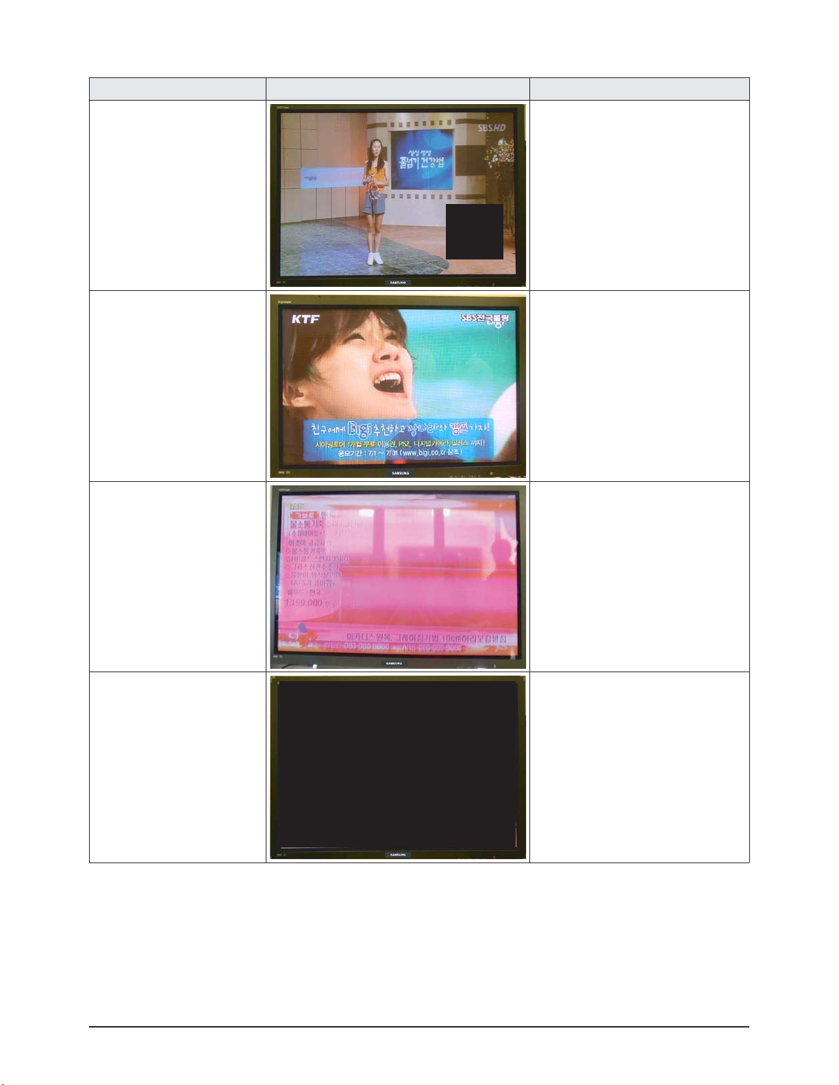
Symptom Related Image Causes and Countermeasures
A blank vertical cell (block)
appears on the screen.
Address buffer defect
- Replace the corresponding upper/lower
buffers (E, F)
COF defect (burnt)
- Replace the module
A green screen appears when
the TV is turned on.
The Scale is not reseting
- Replace the Main board
The OSD box appears but there
is no text.
Incorrect program version
- Check the version of each program
- Replace the Main board
A blank upper (or lower) block
appears on the screen.
Upper/Lower Y Buffer defect
- Replace the corresponding upper/lower
buffers (E, F)
Page 58
Troubleshooting
4-14 Samsung Electronics
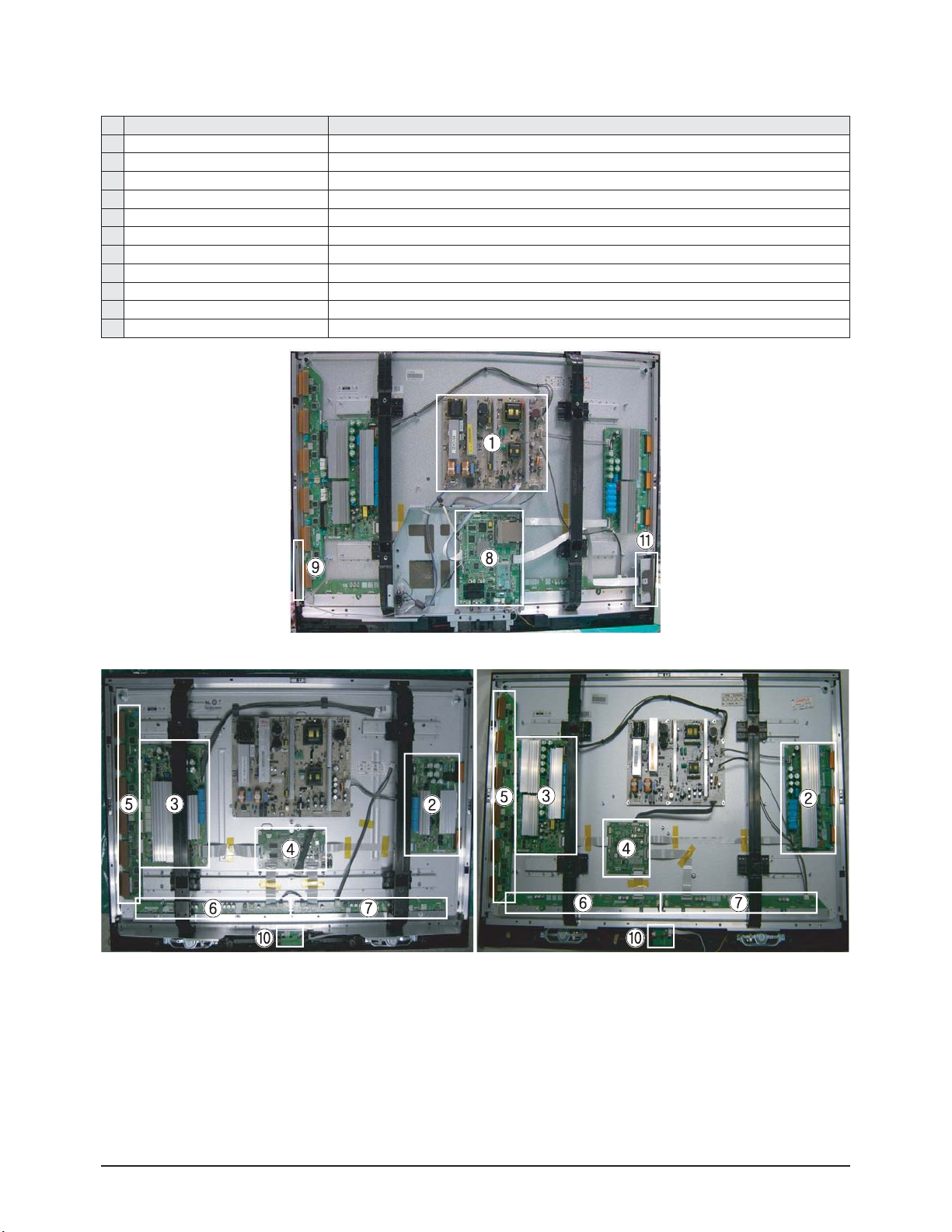
Symptom Related Image Causes and Countermeasures
Either the main or sub picture
does not appear.
Replace the Main board
A vertical green line appears on
the screen.
The SMPS voltage is incorrect
- Adjust the SMPS voltage according to
the voltage printed on the module label
Dim screen (blurred in red) X-Main board defect
- Replace the X-Main board
A blank screen appears - Replace the Y-Main board
Page 59
Troubleshooting
Samsung Electronics 4-15
4-1-4 Troubleshooting Procedures by assembly
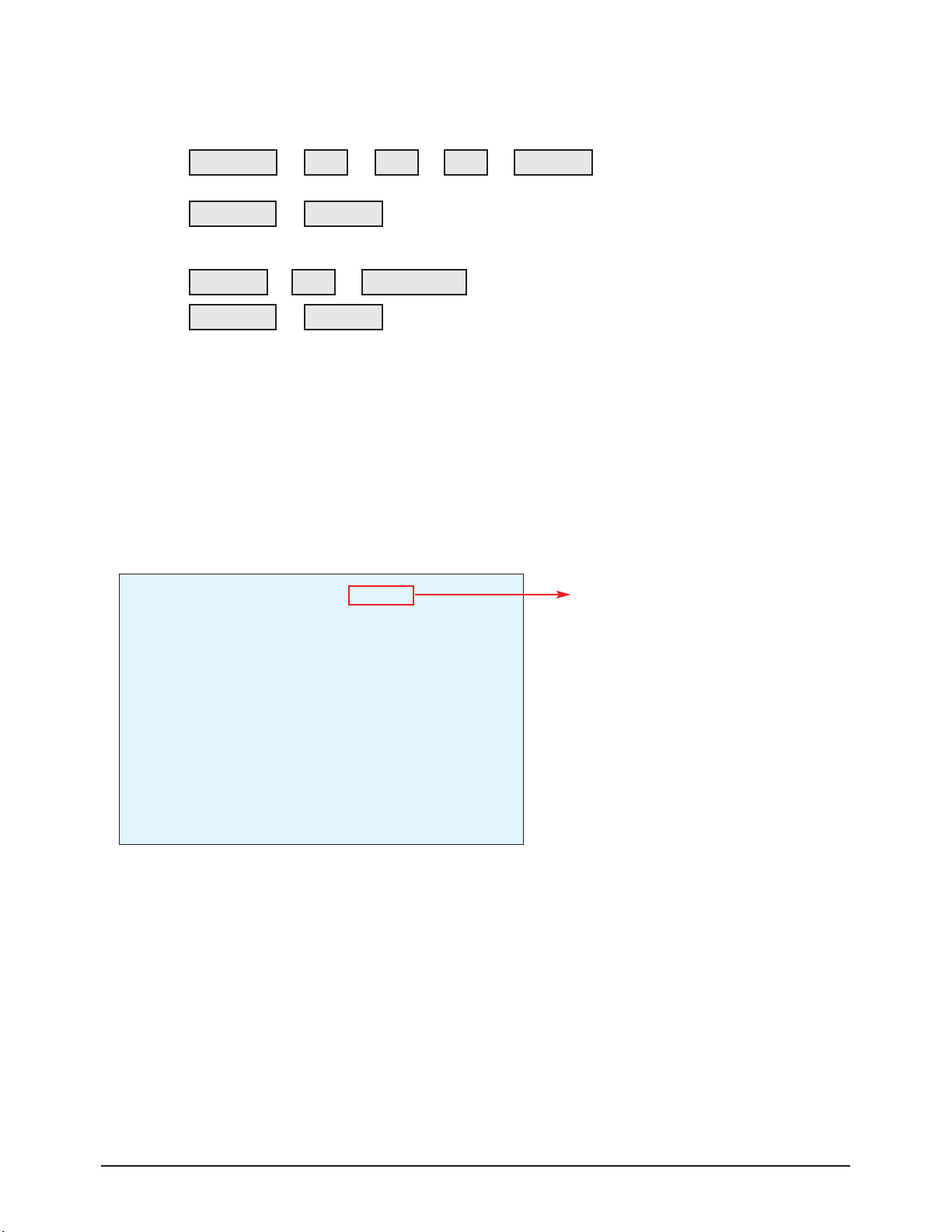
No Assembly Major Symptoms
1 SMPS-PDP TV No power, Blank screen, the Relay repeats On and Off.
2 ASSY PDP MODULE P-X-MAIN Blank screen
3 ASSY PDP MODULE P-Y-MAIN Blank screen
4 ASSY PDP MODULE P-LOGIC MAIN Blank screen, Screen noise
5 ASSY PDP MODULE P-Y-MAIN SCAN BUFFER Row Bar screen is blank
6 ASSY PDP MODULE P-ADDRESS E BUFFER Corresponding Buffer Board block screen is blank.
7 ASSY PDP MODULE P-ADDRESS F BUFFER Corresponding Buffer Board block screen is blank.
8 ASSY PCB MISC-MAIN No Power, Abnormal screen for each input source, PIP screen trouble, Sound trouble
9 ASSY BOARD P-FUNCTION The side function key does not work properly
10 ASSY BOARD P-POWER&IR The remote control does not work properly, the LED does not work properly.
11 ASSY BOARD P-SIDE AV The AV2 and S-VIDEO2 modes do not work properly
<PDP 42”> <PDP 50”>
Page 60

Troubleshooting
4-16 Samsung Electronics
4-2 Adjustment
4-2-1 Service Instruction
■ Before Performing After Sales Services
1. Check if the measurement and test equipment is working properly.
2. Secure sufficient work space for disassembling the product.
3. Prepare a soft pad for disassembling the product.
■ Service adjustment item after replacement of Board
<If adjustment equipment is available>
① PDP Option of Factory Mode → set the Factory Data Type item as the suitable value of relevant model.
② Adjust Calibration of Factory Mode for each mode.
③ Adjust White Balance of Factory Mode.
<If adjustment equipment is not available>
① Write down the value of HDMI White Balance of Factory Mode before replacing Board.
② PDP Option of Factory Mode → set the Factory Data Type item as the suitable value of relevant model.
③ Set the value of HDMI White Balance with the value written down before.
Page 61
Troubleshooting
Samsung Electronics 4-17
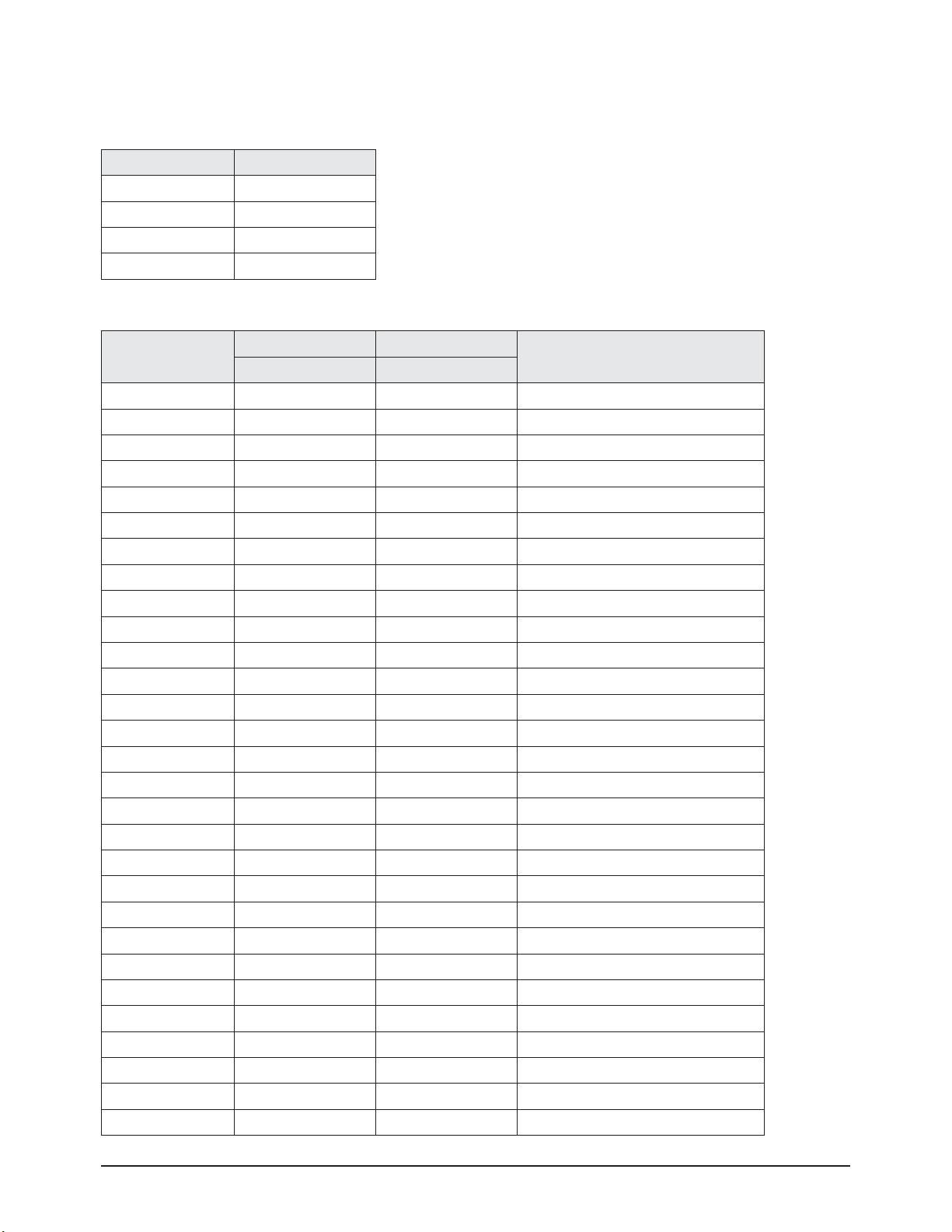
4-2-2 How to Access Service Mode
1. General Remote
To Enter: →→→→
(Interval between key strokes: less than 3 sec)
To Exit: →
2. Factory Remote
To Enter: →→→(Interval between key strokes: less than 3 sec)
To Exit: →
Press the Factory key twice with a key stroke interval of more than 1 second (Pressing once enters Aging Mode)
3. Settings when entering Factory mode
- Sharp Screen (Dynamic), Color Tone (Cool1), Factory (Dynamic CE Off)
4. Adjustment Procedures
- Channel ▲▼Key : Select an item.
- Volume ◀▶ Key : Adjust the value up or down.
- MENU Key : Save the changes to the EEPROM and return to the higher-level mode.
- Using the Numeric (0~9) keys, you can select a channel.
- Using the SOURCE key, you can switch AV modes.
5. Initial SERVICE MODE DISPLAY State
※ The version of the firmware displayed at the bottom of the screen may differ and the firmware is subject to change for the
improvement of product functions.
※ If you have adjusted the settings in Service Mode, you have to reset the product.
POWER OFF INFO POWER ON
POWER OFF POWER ON
POWER OFF POWER ON
MENU MUTE
POWER ON INFO FACTORY Key
Panel ON Time(Hour) 0002 C4A_RMA
1. Calibration 7. YC Delay
2. Option Table 8. Adjust
3. White Balance 9. I2C Check
4. SVP-UX 10. W/B MOVIE
5. Option Block 11. Checksum
6. SGTV5810/NTP3000 12. Reset
13. Spread Specturm
T-CALMPEUH-xxxx (Main Micom Ver)
T-BDPMPEUS-xxxx
BORD2_CALLA_TR-xxxx (TR Ver)
Month / Day / Year / Hour / Min. / Sec.
50": C5A_RMA
Page 62
Troubleshooting
4-18 Samsung Electronics
4-2-3 Factory Data
★★
The underlined are items applied during the service adjustment. None of the others should be adjusted.
1. Calibration
Item Data
AV Calibration Success
Comp Calibration Success
PC Calibration Success
HDMI Calibration Success
2. Option Table(Service)
Item
PDP 42" PDP 50"
Option index
C4A_RMA initial value C5A_RMA initial value
Ready OFF OFF ON / OFF
Inch Option 42" 50" 42" / 50"...
Panel Vender AMLCDINT AMLCDINT AUO/CMO...
Gamma OFF OFF ON / OFF
Panel Type Normal1 Normal1 Normal1 / Normal2...
Model Option Bord Plus Bord Plus Call / Lily / Brod Plus / Jasmine
Tuner SEMCO SEMCO SEMCO / ALPS
Tuner TOP 8 8 0 ~ 31
Auto Power ON ON ON / OFF
Nordic OFF OFF ON / OFF
LNA Menu ON ON ON / OFF
TTX On/Off ON ON ON / OFF
TTX List Flof Flof Flof / List
Carrier Mute OFF OFF ON / OFF
High Deviation OFF OFF ON / OFF
VOL.Curve Small Small Small / Large
HDMI Hotplug 1 1 0 / 1
HDMI Clock CtrI 1 1 0 / 1
HDMI Hotplug Dly 9 9 3~50
Hotel Option
Hotel Mode OFF OFF ON / OFF
Power On Channel 1 1 1 ~ 99
Power On Volume 10 10 1 ~ 100
Max Volume 100 100 1 ~ 100
Local Key Lock OFF OFF ON / OFF
Power On Source RF RF RF/Ext.1...
Shop Mode OFF OFF ON / OFF
Color Space ON ON ON / OFF
PC Ident OFF OFF ON / OFF
Page 63
Troubleshooting
Samsung Electronics 4-19
Item
PDP 42" PDP 50"
Option index
C4A_RMA initial value C5A_RMA initial value
Language English English English / German...
ANYNET+ ON ON ON / OFF
Ch.Table SUWON SUWON SUWON / SESK / SEH / TTSEC
TTX Group Auto Auto Auto / West Europe...
iDTV_Cntry UK UK UK / France...
3. White Balance
Item Range Tv/AV/Scart Comp/iDTV PC HDMI
Sub-Briteness 00H ~ FFH 128 128 128 128
R-offset 00H ~ FFH 128 128 128 128
G-offset 00H ~ FFH 128 128 128 128
B-of
fset
00H ~ FFH 128 128 128 128
Sub-Contrast 00H ~ FFH 128 128 128 128
R-Gain 00H ~ FFH 128 128 128 128
G-Gain 00H ~ FFH 128 128 128 128
B-Gain 00H ~ FFH 128 128 128 128
Range
00H ~ FFH
Item Range RF AV
Comp
480i
Comp
480p
Comp
720p
Comp
1080i
HDMI PC iDTV
H2Gain 00 ~ 1FH 05H 05H 05H 05H 04H 04H 0AH 05H 05H
H4Gain 00 ~ 1FH 04H 0AH 05H 05H 02H 02H 0AH 05H 05H
V2Gain 00 ~ 1FH 0CH 0CH 0AH 0CH 0AH 0AH 10H 0AH 0AH
V4Gain 00 ~ 1FH 0CH 10H 0CH 0CH 0AH 0AH 10H 0AH 0AH
Sr2Gain 00 ~ 1FH 00H 00H 00H 00H 00H 00H 00H 00H 00H
Sr4Gain 00 ~ 1FH 00H 02H 00H 00H 02H 02H 04H 02H 02H
Sl2Gain 00 ~ 1FH 00H 00H 00H 00H 00H 00H 00H 00H 00H
Sl4Gain 00 ~ 1FH 00H 02H 00H 00H 02H 02H 04H 02H 02H
Peakth1 00H ~ FFH 06H 02H 03H 03H 03H 03H 03H 08H 04H
Peakth2 00H ~ FFH 2FH 2FH 2FH 2FH 2FH 2FH 2FH 2FH 2FH
Peskth3 00H ~ FFH 3FH 3FH 3FH 3FH 3FH 3FH 3FH 3FH 3FH
4. SVP-UX
① ComB Filter
Item
Y-Filter
② Sharpness
Page 64
Item Range TV/AV/S_Video Component PC HDMI
R-Offset 00H ~ FFH 3AH 40H 32H 82H
G-Offset 00H ~ FFH 3AH 40H 32H 82H
B-Offet 00H ~ FFH 3AH 40H 32H 82H
R-Gain 00H ~ FFH A6H 92H A9H 6CH
G-Gain 00H ~ FFH A6H 92H A9H 6CH
B-Gain 00H ~ FFH A6H 92H A9H 6CH
④ RGB Calibration
Item Range TV/AV/S_Video Component PC HDMI
TCD3 Contrast 00H ~ FFH 79H 78H 78H 78H
TCD3 Brightness 00H ~ FFH 29H 20H 20H 20H
TCD3 CR 00H ~ FFH 80H 80H 80H 80H
TCD3 CB 00H ~ FFH 80H 80H 80H 80H
TCD3 Delay 00H ~ FFH 00H 00H 00H 00H
Analog Y Offset 00H ~ FFH 40H 3DH 44H 40H
Analog PB Offset 00H ~ FFH 80H 80H 44H 80H
Analog PR Offset 00H ~ FFH 80H 80H 44H 80H
Analog Y Gain 00H ~ FFH D6H B3H A4H 80H
Analog PB Gain 00H ~ FFH 80H B3H ACH 80H
Analog PR Gain 00H ~ FFH 80H B3H A7H 80H
Black Level 00H ~ FFH 00H 00H 00H 00H
Svp Brightness 00H ~ FFH 00H 00H 00H 00H
⑤ ADC Calibration
Item Range low high Delta
AV ADC 00H ~ FFH 10H DCH 02H
COMP ADC 00H ~ FFH 10H EBH 02H
PC ADC 00H ~ FFH 10H DCH 04H
ALL RGB 00H ~ FFH 01H EBH 0AH
⑥ Calibration Target
Troubleshooting
4-20 Samsung Electronics
Item Range Initial value
Y_NR_OFF 00H ~ FFH 00H
C_NR_OFF 00H ~ FFH 00H
Y_NR_ON 00H ~ FFH 00H
C_NR_ON 00H ~ FFH 00H
③ NR
Page 65
Troubleshooting
Samsung Electronics 4-21
Item Range Initial value
Skin Direction Reddish / Yellowish Reddish
Skin Enhance 00H ~ FFH 00H
Green Stretch 00H ~ FFH 00H
Blue Stretch 00H ~ FFH 00H
⑦ Color Management
5. Option Block
① FRC(Micronas)
② FRC2X
Item Range Initial value
OUTCON 1 ~ 3 0
GAMMA 1 ~ 7 0
OCC_MODE 0 / 1 0
FALLBACK 0 / 1 0
DBG_MARK 0 / 1 0
SPR_CBR 0 / 1 0
BIT_EXPAND 0 / 1 0
INV_BIT_EXPAND 0 / 1 0
REPEAT_MODE 0 / 1 0
DEMO_ON_OFF 0 / 1 0
MMU_RD_START 00H ~ FFH 00H
ME_RD_START 00H ~ FFH 00H
MC_RD_START 00H ~ FFH 00H
CMZL(0x36E) 00H ~ FFH 0H
BLOL(0x2A7) 00H ~ FFH 0H
LOGO(0x2A7) 00H ~ FFH 0H
Page 66
Troubleshooting
4-22 Samsung Electronics
③ FBE2
ITEM Range RF
AV/
S-Video
Comp
480i/576i
Comp
480p/576p
Comp
720p/108
0i/1080p
HDMI DTV PC
Pattern Select 0 ~ 20 0 0 0 0 0 0 0 0
BS-On 0 / 1 1 1 1 1 1 1 1 1
B-Slope Gain 0 ~ 255 34 44 64 64 64 64 64 64
B-Tilt Min 0 ~ 255 20 20 20 20 20 20 20 20
B-Tilt Max 0 ~ 255 120 120 120 120 120 120 120 120
B-Tilt Slope 0 ~ 255 128 128 128 128 128 128 128 128
LFunc-Basis 0 ~ 255 30 20 50 40 70 55 75 55
Hfunc-Basis 0 ~ 255 30 40 50 40 75 65 88 65
Mean-Offset1 0 ~ 255 20 100 75 75 75 75 75 75
Mean Offset2 0 ~ 255 120 200 155 155 225 225 225 225
Mean Slope 0 ~ 255 56 56 45 45 85 85 85 85
Input Offset 0 ~ 255 128 128 128 128 128 128 128 128
Input Gain 0 ~ 255 128 128 128 128 128 128 128 128
ACR Offset 0 ~ 128 15 15 15 15 15 15 15 15
ACR Th1 0 ~ 255 30 30 30 30 30 30 30 30
ARC Th2 0 ~ 255 130 130 100 130 130 130 130 130
Skin Enable 0 / 1 1 1 1 1 1 1 1 1
Skin Tu 0 ~ 255 165 165 150 150 165 165 128 165
Skin Tv 0 ~ 255 140 140 140 140 128 128 128 128
M Skin Tu 0 ~ 255 128 128 128 128 128 128 128 128
M Skin TV 0 ~ 255 128 128 128 128 128 128 128 128
Sub Color 0 ~ 255 115 128 135 135 140 150 143 150
M-Au-Sub Color 0 ~ 255 128 128 128 128 128 128 128 128
M-Wi-Sub Color 0 ~ 255 128 128 128 128 128 128 128 128
MW-Skin-Tu 0 ~ 255 128 128 128 128 128 128 128 128
MW-Skin-Tv 0 ~ 255 128 128 128 128 128 128 128 128
Page 67
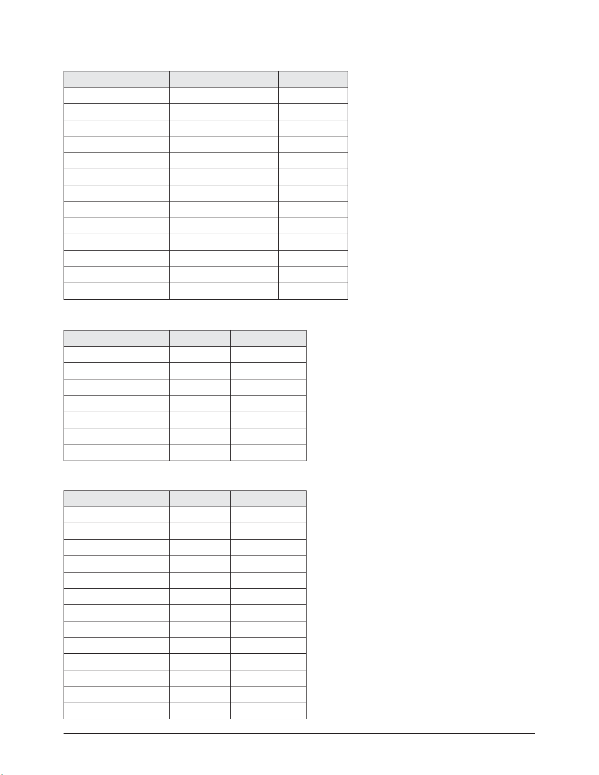
Troubleshooting
Samsung Electronics 4-23
ITEM Range Initial value
Pattern Srlect 0 ~ 63 0
Data updata ON / OFF OFF
Data Type 42"EU MRT/42"EU MESH/... 42"EU MRT
CDC Sw ON / OFF OFF
CDC Strengh Th 0 ~ 31 0
BRE Sw ON / OFF OFF
FRC Repeat Mode ON / OFF OFF
FRC CBG Mark On 0 ~ 15 0
ERC Bypass ON / OFF OFF
Panel Type - 0H
Panel Inch - SD
Panel Version -
Logic Sw Version - 0H 0H 0H
④ Pdp Logic
ITEM Range Initial value
ID Tone Shift 1H ~ FH 01H
ID Tone Thresh 00H ~ FFH 7FH
Demod Prescaler 00H ~ 20H 13H
Master Volume 00H ~ 30H 13H
PWM Modulation 80H ~ F2H F1H
DRC Threshold 00H ~ 7FH 06H
Speaker EQ ON / OFF OFF
6. SGTV5810/NTP3000
ITEM Range Initial value
RF PAL-B/G 00H ~ FFH AAH
RF PAL-D/K 00H ~ FFH 99H
RF PAL-I 00H ~ FFH 99H
RF SECAM-B/G 00H ~ FFH 88H
RF SECAM-D/K 00H ~ FFH 44H
RF SECAM-L/L' 00H ~ FFH 88H
RF NTSC 3.58 00H ~ FFH 44H
RF NTSC 4.43 00H ~ FFH CCH
AV PA L 00H ~ FFH AAH
AV SECAM 00H ~ FFH 88H
AV NTSC 3.58 00H ~ FFH 30H
AV NTSC 4.43 00H ~ FFH AAH
AV PAL60 00H ~ FFH 77H
7. YC Delay
Page 68
Troubleshooting
4-24 Samsung Electronics
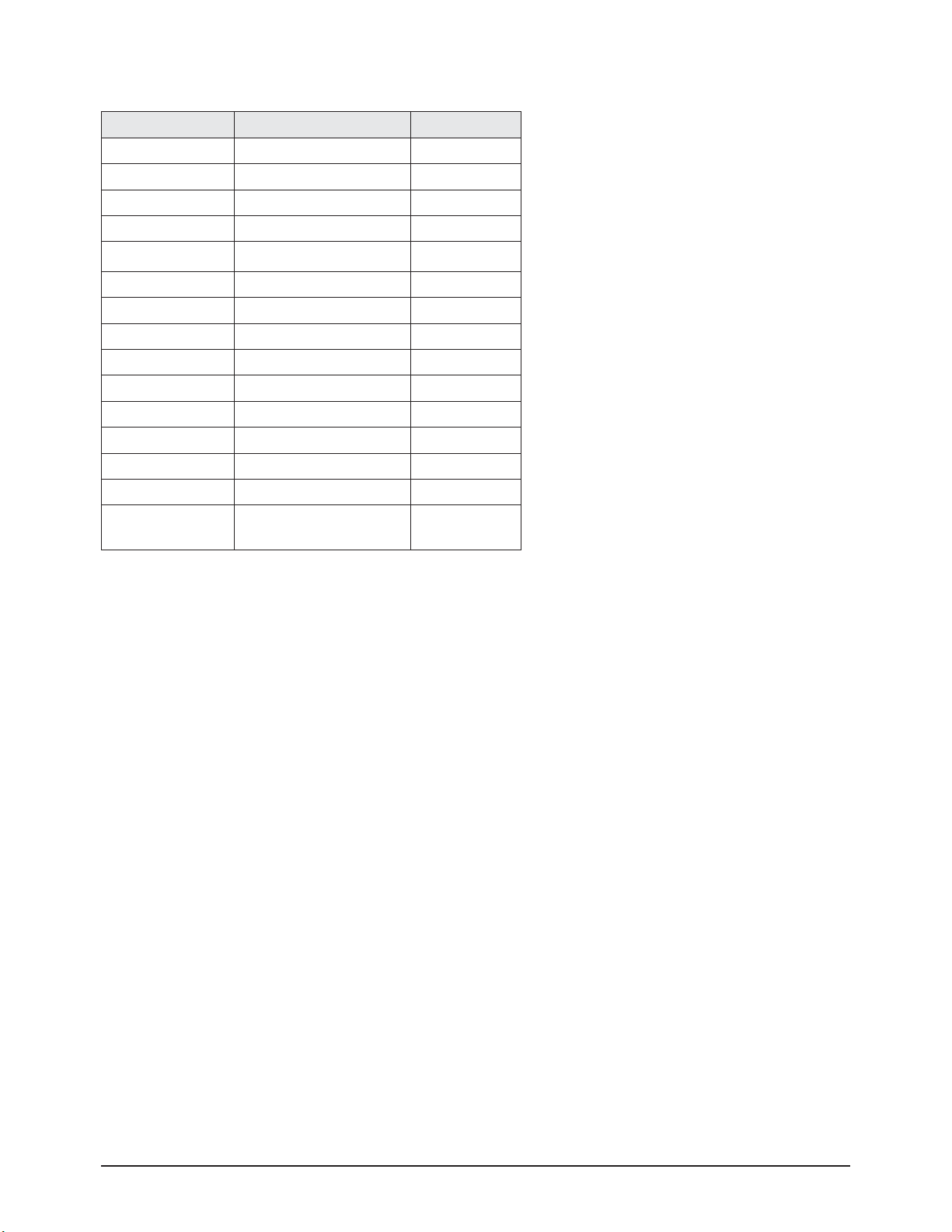
8. Adjust
9. I2C Check
ITEM Range Initial value
Video Mute Time 0 ~ 255 10
Dynamic Contrast ON / OFF ON
Dynamic Dimming ON / OFF ON
Dynamic CE ON / OFF OFF
LNA PLUS
RFDB-1 Level 0 ~ 255 2
RFDB-2 Level 0 ~ 255 5
RFDB-3 Level 0 ~ 255 7
RFDB-4 Level 0 ~ 255 24
Magazine LNA ON / OFF OFF
PixelShift Test ON / OFF OFF
Debug ON / OFF OFF
ACR ON / OFF OFF
D-Watchdog ON / OFF ON
UART Select
MAIN / IDTV / PDP Lvds ON
/ PDP Lvds /OFF
OFF
Page 69
Troubleshooting
Samsung Electronics 4-25
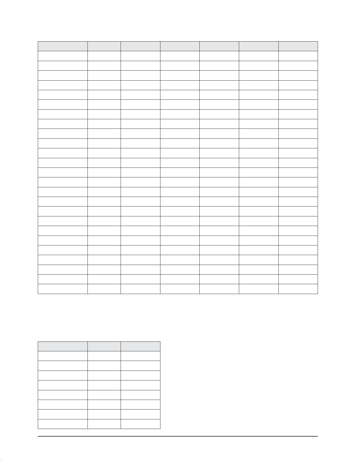
10. W/B MOVIE
ITEM Range TV/AV/S_Video Component PC HDMI Scart1/2
WB Movie ON / OFF OFF OFF OFF OFF OFF
Color Mode Movie Movie Dynamic Dynamic Dynamic Dynamic
Color Tone Cool1 Cool1 Cool1 Cool1 Cool1
Msub Brigh 0 ~ 255 128 128 128 128 128
Msub Contr 0 ~ 255 128 128 128 128 128
W1_RGAIN 0 ~ 255 157 161 144 161 157
W1_BGAIN 0 ~ 255 76 74 11 7 76 76
W1_R_OFFS 0 ~ 255 11 9 11 9 127 118 11 9
W1_B_OFFS 0 ~ 255 138 140 11 0 141 138
W2_RGAIN 0 ~ 255 142 143 149 142 142
W2_BGAIN 0 ~ 255 48 47 93 51 48
W2_R_OFFS 0 ~ 255 129 127 124 128 129
W2_B_OFFS 0 ~ 255 143 145 11 0 143 143
NO_RGAIN 0 ~ 255 141 139 137 141 141
NO_BGAIN 0 ~ 255 104 102 123 104 104
NO_R_OFFS 0 ~ 255 126 125 126 121 126
NO_B_OFFS 0 ~ 255 136 133 11 4 133 136
C2_RGAIN 0 ~ 255 124 122 123 125 124
C2_BGAIN 0 ~ 255 142 141 156 143 142
C2_R_OFFS 0 ~ 255 128 129 117 128 128
C2_B_OFFS 0 ~ 255 128 127 116 128 128
Movie Contr 0 ~ 100 100 100 100 100 100
Movie Brigh 0 ~ 100 45 45 45 45 45
Movie Color 0 ~ 100 55 55 55 55 55
Movie Sharp 0 ~ 100 75 75 75 75 75
11. Checksum xxxx
12. Reset
13. Spread Spectrun
ITEM Range Initial value
Spectrum ON / OFF ON
Delta -128 ~ +128 0
Positive 0 ~ 99 8
Negative 0 ~ 99 2
Speed 0 ~ 7 0
Time 0 ~ 7 4
FBE Spectrum ON / OFF OFF
FEE Delta 0 ~ 5 0
Page 70

Troubleshooting
4-26 Samsung Electronics
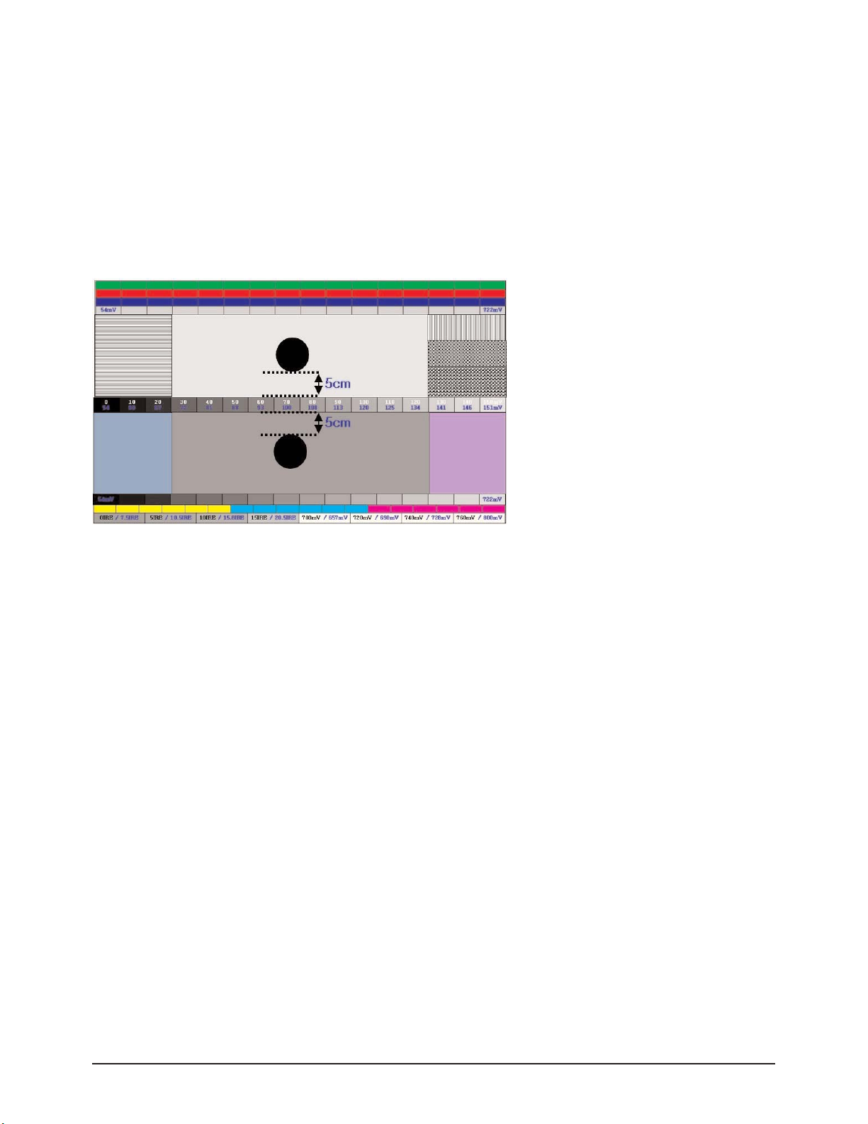
( Chess Pattern )
4-2-4 Service Adjustment
■
■
White Balance - Calibration
If picture color is wrong, do calibration first.
Execute calibration in Factory Mode
1. Source : VIDEO
2. Setting Mode : PAL Video (MODE : #2)
3. Pattern : Pattern #24 (Chess Pattern)
4. Use Equipment : K-7256 or Equipment of equality level
5. Work order
1) Enter by Factory Mode select "1. CALIBRATION".
2) Select "AV CALIBRATION" again in CALIBRATION MENU.
3) After Completing Calibration, come out "Av success". OSD on the screen (bottom-side) for about 3 seconds.
Source AV : PAL composite, Component : 1280*720/60Hz
PC : 1024*768/60Hz
Page 71
Troubleshooting
Samsung Electronics 4-27
■
■
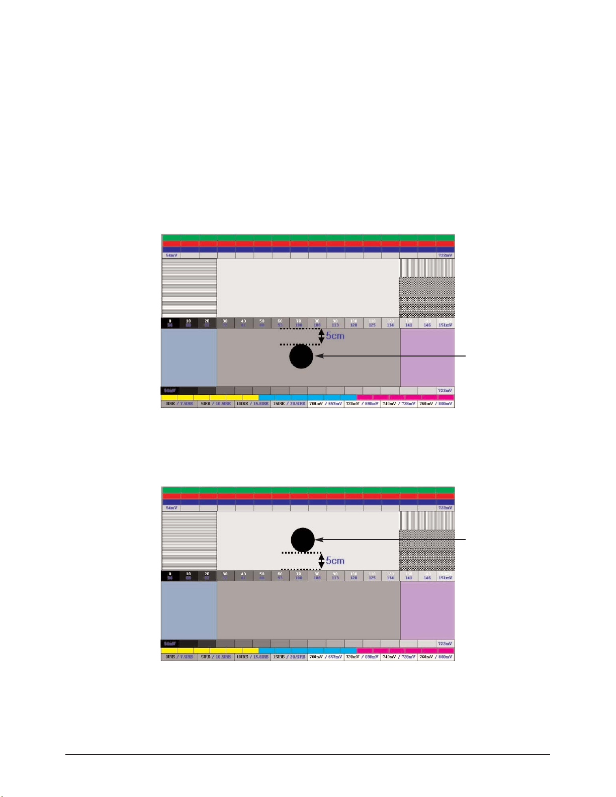
White Balance - Adjustment
If picture color is wrong, check White Balance condition.
Equipment : CA210, Patten : Toshiba
Adjust W/B in Factory Mode
Sub brightness and R/G/B Offset controls low light region
Sub contrast and R/G/B Gain controls high light region
Source AV : PAL composite, Component : 1280*720/60Hz,
HDMI[DVI] : 1280*720/60Hz
[ Test Pattern : MSPG-945 Series Pattern #16 ]
* Color temperature
1500K +/-500, -6 ~-20 MPCD
* Color coordinate
H/L : 270/280 +/- 2
L/L : 270/280 +/- 3, 2.1 Ft +/-0.05 Ft
( SAMSUNG WHITE BALANCE Adjustment PATTERN with FPD )
■
Conditions for Measurement
1. On the basis of toshiba ABL pattern : High Light level (57 IRE)
- INPUT SIGNAL GENERATOR : MSPG-925LTH
* Mode No 2 : 744X484@60 Hz
No 6 : 1280X720@60 Hz
No 21 : 1024X768@60 Hz
* Pattern No 36 : 16 Color Pattern
No 16 : Toshiba ABL Pattern
2. Optical measuring device : CA210 (FL)
Please use the MSPG-925 LTH generator for model PS-42Q96HD, PS-50Q96HD.
Page 72
Troubleshooting
4-28 Samsung Electronics
■
■
Method of Adjustment
1. Adjust the white balance of AV, Component and DVI Modes.
(AV
→ Component)
a) Set the input to the mode in which the adjustment will be made (RF → DTV → PC → DVI).
* Input signal - VIDEO Mode : Model #2 (744*484 Mode), Pattern #16
- DTV, DVI Mode : Model #6 (1280*720 Mode), Pattern #16
- HDMI Mode : Model #6 (1280*720 Mode), Pattern #16
b) Enter factory color control, confirm the data.
c) Adjust the low light. (Refer to table 1, 2 in adjustment position by mode)
- Adjust sub - Brightness to set the 'Y' value.
- Adjust red offset ('x') and blue offset ('y') to the color coordinates.
* Do not adjust green offset data.
d) Adjust the high light. (Refer to table 1, 2 in adjustment position by mode)
- Adjust red gain ('x') and blue gain ('y') to the color coordinates.
* Do not adjust the green gain and sub-contrast (Y) data.
( SAMSUNG WHITE BALANCE Adjustment PATTERN with FPD )
( SAMSUNG WHITE BALANCE Adjustment PATTERN with FPD )
Low light
Measurement point
Hight light
Measurement point
Page 73
Troubleshooting
Samsung Electronics 4-29
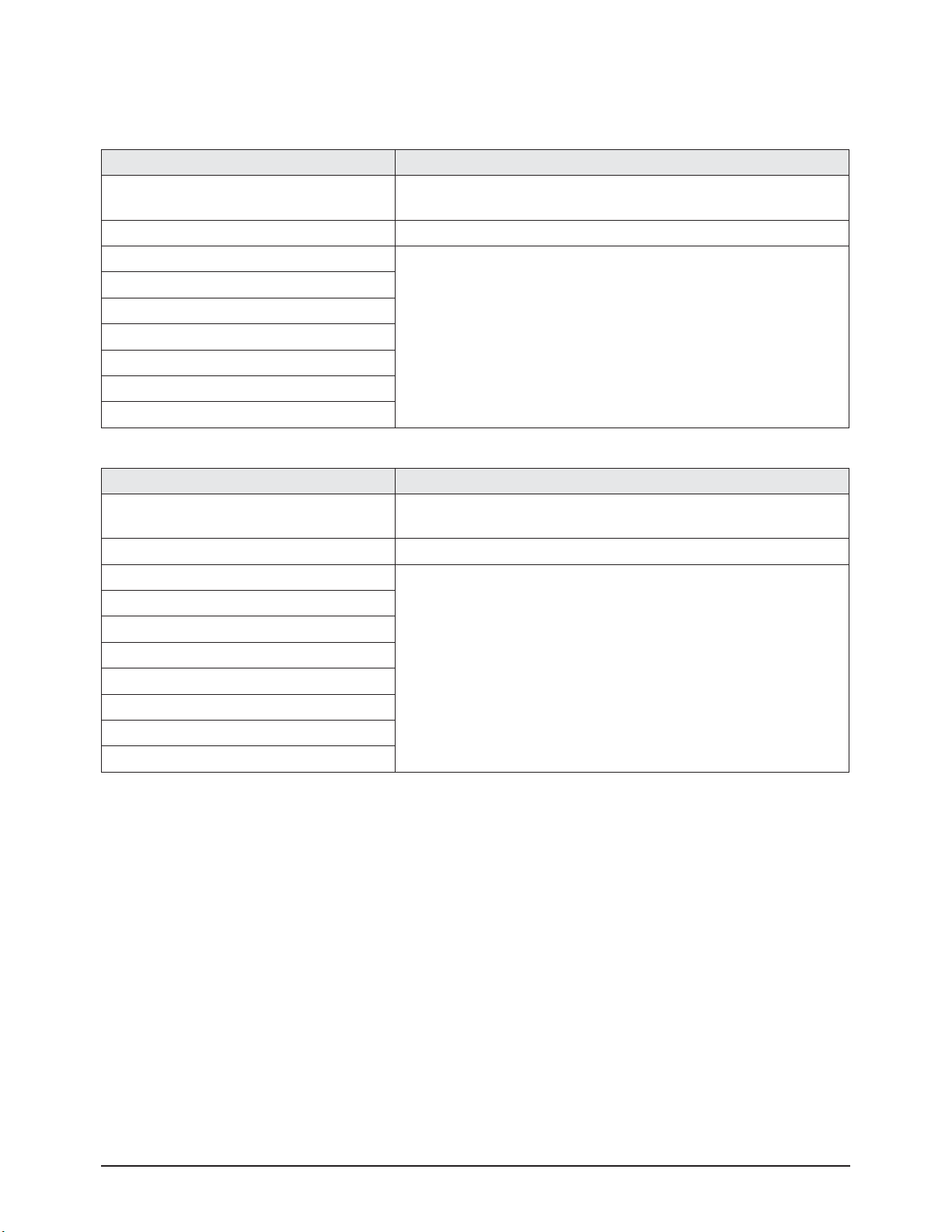
Replaced assembly items Check Items
ASSY PCB MISC-MAIN
1) Auto Program
2) White Balance Adjust
SMPS-PDP TV Vs, Va voltage check and adjust
ASSY PDP MODULE P-LOGIC MAIN
Not to be adjusted
ASSY PDP MODULE P-X-MAIN
ASSY PDP MODULE P-Y-MAIN
ASSY PDP MODULE P-Y-MAIN SCAN BUFFER
ASSY PDP MODULE P-ADDRESS E BUFFER
ASSY PDP MODULE P-ADDRESS F BUFFER
ASSY BOARD P-SIDE A/V
* PDP 50" Check items listed after changing each
Replaced assembly items Check Items
ASSY PCB MISC-MAIN
1) Auto Program
2) White Balance Adjust
SMPS-PDP TV Vs, Va voltage check and adjust
ASSY PDP MODULE P-LOGIC MAIN
Not to be adjusted
ASSY PDP MODULE P-X-MAIN
ASSY PDP MODULE P-Y-MAIN
ASSY PDP MODULE P-Y-MAIN SCAN BUFFER
ASSY PDP MODULE P-Y-MAIN SCAN BUFFER
ASSY PDP MODULE P-ADDRESS E BUFFER
ASSY PDP MODULE P-ADDRESS F BUFFER
ASSY BOARD P-SIDE A/V
※ When replacing the SMPS or PDP panel, you have to check the voltage printed on the panel sticker and adjust it.
4-2-5 Replacements & Calibration
* PDP 42" Check items listed after changing each
Page 74
Troubleshooting
4-30 Samsung Electronics
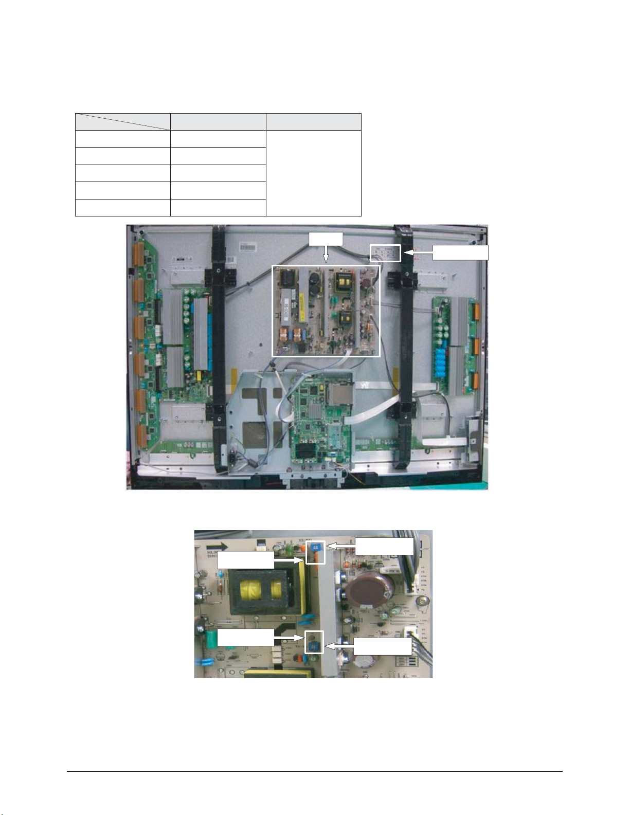
2. A point of adjusting SMPS-MAIN voltage.
Value Board Adjustment
Vs 210
SMPS
Va 63
Vset -
Ve 94
Vscan -190
■
Voltage Adjustment
1. After replacing the SMPS or PDP panel, you must adjust the voltage referring to the voltage label printed on the panel.
(If you do not adjust the voltage, an abnormal discharge symptom may appear.)
SMPS
Voltage Label
Vs Adjustment
Vs Test point
Va Test point
Va Adjustment
Page 75
Troubleshooting
Samsung Electronics 4-31
■
■
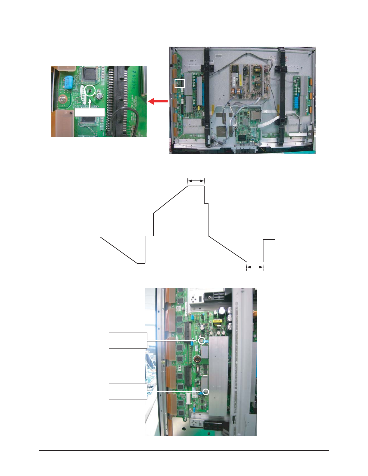
Y-RR and Y-FR controls
Set the main reset (rising : 60usec, falling : 80usec) by change the value of variable resistor.
Test Point
60usec
Rising ramp
variable resistor
Falling ramp
variable resistor
80usec
Page 76
Troubleshooting
4-32 Samsung Electronics
4-3 Upgrade
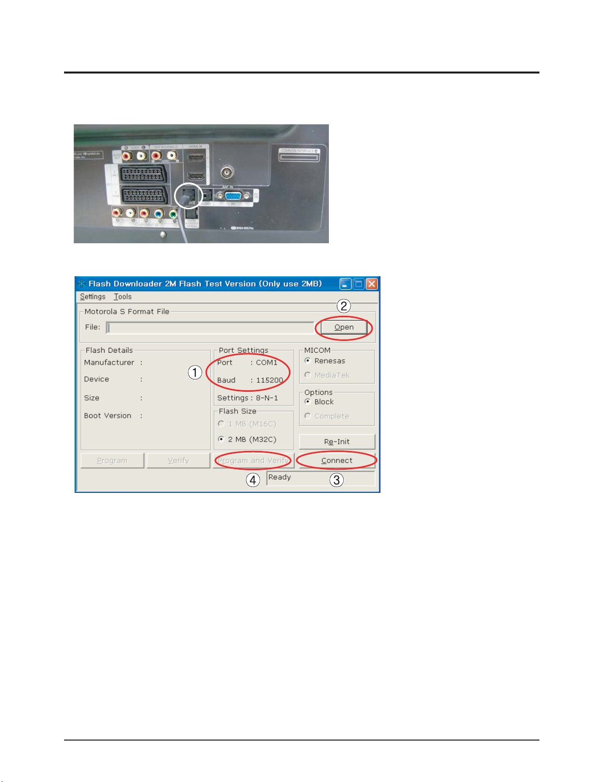
4-3-1 How to Update Flash ROM (with RS-232C Cable)
1. Connect Set (Service Jack) and Jig Cable to execute Program Update.
2. Turn Off (On Stand by mode) the Set
- Run Down load tool
1) Check ①
2) Select MOT file by Open ②
3) Click Connect Button ③
4) Turn On the Set
5) Click ④
3. Turn off (= AC Power off) the Set (waiting a few seconds) and turn on again.
S/W Down Load Time: 6min
Page 77
Troubleshooting
Samsung Electronics 4-33
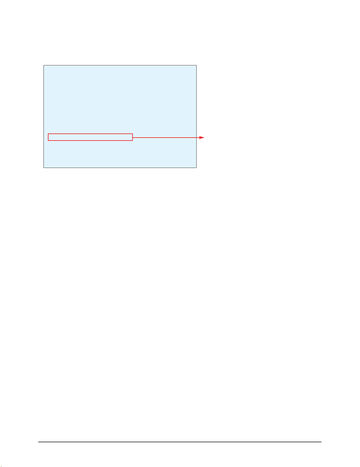
4-3-2 How to Check the Version of the Program
1. Procedures for checking in the Factory Menu.
When entering Factory Mode, the version of the software is displayed at the bottom of the menu as described on page 4-17.
Panel ON Time(Hour) 0002 C4A_RMA
1. Calibration 7. YC Delay
2. Option Table 8. Adjust
3. White Balance 9. I2C Check
4. SVP-UX 10. W/B MOVIE
5. Option Block 11. Checksum
6. SGTV5810/NTP3000 12. Reset
13. Spread Specturm
T-CALMPEUH-xxxx (Main Micom Ver)
T-BDPMPEUS-xxxx
BORD2_CALLA_TR-xxxx (TR Ver)
Month / Day / Year / Hour / Min. / Sec.
S/W Version
Page 78
Wiring Diagram
Samsung Electronics 6-1
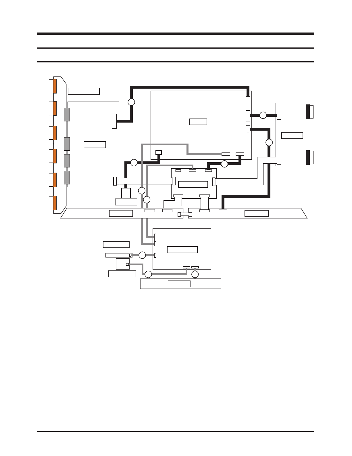
6. Wiring Diagram
6-1 Overall Wiring
<42" Overall Wiring>
CN5401
CN5402
CN5403
CN5501
CN5502
CN5503
Y-MAIN SCAN
CN5407
CN5408
Y-DRIVE
CN5409
CN5412
CN5707
CN5701
E-BUFFER
FUNCTION
4
AC-INLET
CN1
CN3
CN810
CN4002
CN809
5
CN4701
SMPS
CN808
X-DRIVE
6
CN800
11
CN2000CN2001CN2006
CN2002
2
LOGIC BOARD
CN2028
CN2004
CN801
CN2003
?
CN807
CN4001
7
CN4004
1
CN2500CN2509
CN2202
CN1101
CN2510
CN2610
CN2600
CN2609
F-BUFFER
MAIN BOARD
10
CN1605
CN1606
CN1203
POWER SW
8 9
SPEAKER
Page 79
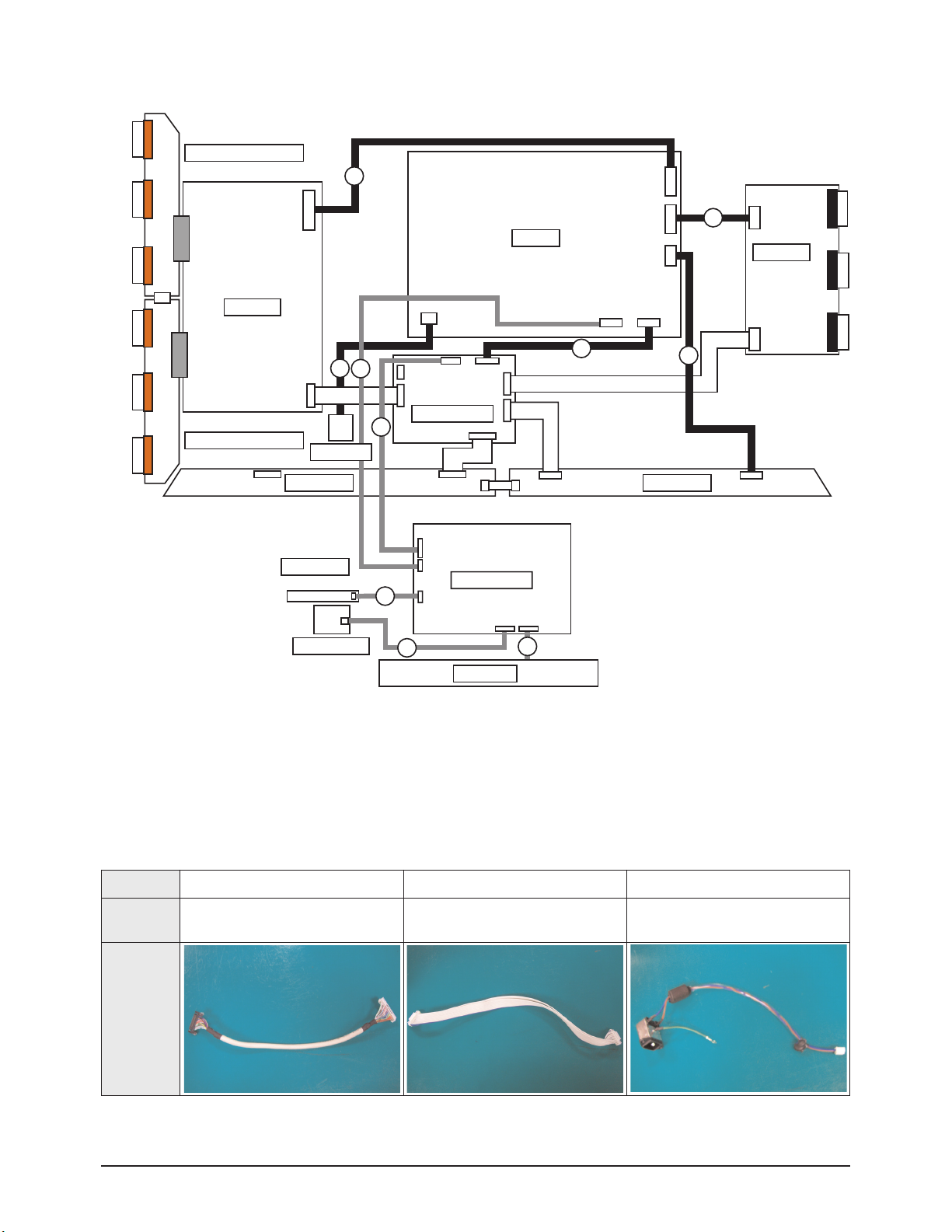
<50" Overall Wiring>
※ The code number of cable(Lead-connector) can be changed, see "5. Exploded View & Part List."
Wiring Diagram
6-2 Samsung Electronics
Use
① LVDS 31P-30P ② POWER 24P ⑪ AC_INPUT
Code BN39-00859A BN39-00881A
42" - 2901-001378
50" - 2901-001340
Photo
CN5401
CN5402
CN5403
CN5412
CN5501
CN5502
CN5503
Y-MAIN SCAN(HIGH)
CN5707
CN5407
Y-DRIVE
CN5507
CN5701
Y-MAIN SCAN(LOW)
11
AC-INLET
E-BUFFER
FUNCTION
CN3
CN1
4
CN810
CN809
CN4002
5
CN4701
SMPS
CN2609
X-DRIVE
CN4004
CN4001
CN4000
CN808
CN800
7
2
CN2006
CN2002
LOGIC BOARD
1
CN2202
CN1101
CN2004
CN2500CN2509
CN2000CN2001
CN2510
CN2003
CN2005
CN2600
CN2610
CN801
CN807
6
F-BUFFER
MAIN BOARD
10
CN1605
CN1606
CN1203
POWER SW
8
9
SPEAKER
Page 80
Wiring Diagram
Samsung Electronics 6-3
①
CN2202(MAIN B'D) ↔ CN2001(LOGIC B'D)
Pin No. Signal Pin No. Signal
1 RxIN0- 16 NC
2 RxIN0+ 17 GND
3 RxIN1- 18 WP
4 RxIN1+ 19 SCL
5 RxIN2- 20 SDA
6 RxIN2+ 21 LVDS Opt
7 RxINCLK- 22 DCC Opt
8 RxINCLK+ 23 GND
9 RxIN3- 24 GND
10 RxIN3+ 25 GND
11 NC 26 Vdd
12 NC 27 Vdd
13 NC 28 Vdd
14 NC 29 Vdd
15 NC 30 Vdd
②
CN1101(MAIN B'D) ↔ CN801(MAIN SMPS)
Pin No. Signal Pin No. Signal
1 PS_ON 13 5V
2 N/C (Auto_V) 14 5V
3 STBY 15 5V
4 GND_STBY 16 5V
5 GND_18V AMP 17 GND_12V
6 GND_18V AMP 18 GND_12V
7 18V AMP 19 12V
8 18V AMP 20 GND_12V
9 GND_5V 21 12V
10 GND_5V 22 12V
11 GND_5V 23 N.C(FAN_ON)
12 GND_5V 24 N.C(FAN_DET)
③
CN1404(MAIN B'D) ↔ CN101(SIDE AV)
Pin No. Signal Pin No. Signal Pin No. Signal Pin No. Signal
1 GND 12 TXC- 23 NC 34 VIDEO_SR_IN
2 TX2+ 13 GND 24 NC 35 VIDEO_SL_IN
3 TX2- 14 MICOM_CEC 25 GND 36 HP_IDENT
4 GND 15 GND 26 SVHS_IDENT 37 HP_OUT_R
5 TX1+ 16 TSCL 27 SVHS_Y 38 HP_OUT_L
6 TX1- 17 TSDA 28 GND 39 USB_VCC
7 GND 18 LSCL 29 SVHS_C 40 B1.8V
8 TX0+ 19 HDMI3_5V 30 GND 41 B3.3V
9 TX0- 20 HPD_SIL9185 31 VIDEO_IDENT
10 GND 21 DDC_WP 32 VIDEO_CVBS
11 TXC+ 22 GND 33 GND
6-1-1 Pin Connection
Page 81
Wiring Diagram
6-4 Samsung Electronics
④
CN810(SMPS)
↔
CN5707(Y B'D)
Pin No. Signal
1 Vg
2 GND
3 GND
4 GND
5 Vs
6 Vs
⑤
CN809(SMPS)
↔
CN4701(X B'D)
Pin No. Signal
1 Vg
2 GND
3 GND
4 Vs
5 Vs
⑥
CN808(SMPS)
↔
CN2609(E-BUFFER)
Pin No. Signal
1 Va
2 GND
3 5.3V
⑨
CN1203(MAIN B'D)
↔
SPEAKER
Pin No. Signal
1 R+_OUT
2 R-_OUT
3 L+_OUT
4 L-_OUT
⑩
CN1605(MAIN B'D)
↔
FUNCTION
Pin No. Signal
1 KEY_INPUT1
2 KEY_INPUT2
3 GND
⑪
CN800(SMPS)
↔
AC INLET
Pin No. Signal
1 AC Neutral
2 N/C
3 AC Live
⑦
CN807(SMPS)
↔
CN2000(LOGIC B'D)
Pin No. Signal
1 STBY
2 VS_ON
3 N/C
4 PS_ON
5 RTN
6 5.3V
7 RTN
8 RTN
9 5.3V
10 5.3V
⑧
CN1606(MAIN B'D)
↔
POWER&IR
Pin No. Signal
1 IR
2 GND
3 A5V_1
4 LED_STB
5 BUZZER
6 KEY_INPUT1
7 KEY_INPUT2
8 GND
9 B5V
10 LED_CTRL
Page 82
Wiring Diagram
Samsung Electronics 6-5
42" Loc. No. 50" Loc. No. Description
CN5401 CN5401 Horizontal Y-scan line(1~128) of Module and Y-Main Scan Connect
CN5402 CN5402 Horizontal Y-scan line(129~256) of Module and Y-Main Scan Connect
CN5403 CN5403 Horizontal Y-scan line(256~384) of Module and Y-Main Scan Connect
- CN5512 Y-Main Scan(High) and Y-Main Scan(Low) Connect
CN5501 CN5501 Horizontal Y-scan line(384~512) of Module and Y-Main Scan Connect
CN5502 CN5502 Horizontal Y-scan line(512~640) of Module and Y-Main Scan Connect
CN5503 CN5503 Horizontal Y-scan line(640~768) of Module and Y-Main Scan Connect
CN5407 CN5407 Upper Y-Drive and Y-Main Scan Connect
CN5507 CN5507 Lower Y-Drive and Y-Main Scan Connect
CN5707 CN5707 Vs(205V),Vg(15v) Power input connect(6Pin) of Y-Drive
CN5701 CN5701 Y-Drive control signal from Logic Board
CN810 CN810 Vs(205V),Vg(15v) Power input connect(6Pin) of SMPS for Y-Drive
CN809 CN809 Vs(205V),Vg(15v) Power input connect(6Pin) of SMPS for X-Drive
CN808 CN808 Va(63V) ,5.3V Power input connect(3Pin) of SMPS for F-Buffer
CN807 CN807 Power input connect(10pin) for Logic Board
CN801 CN801 Image signal(LVDS) connect(41pin) from Main Board
CN800 CN800 AC Power input connect from AC-inlet
CN4002 CN4002 Horizontal X-scan line of Module and X-scan Connect(first Block)
CN4001 CN4001 Horizontal X-scan line of Module and X-scan Connect(second Block)
- CN4000 Horizontal X-scan line of Module and X-scan Connect(third Block)
CN2000 CN2000 Power input connect(10pin) of Logic Board from SMPS
CN2001 CN2001 Image signal(LVDS) connect(41pin) of Logic board from Main Board
CN2002 CN2002 Y-Drive control signal of Logic Board
CN2004 CN2005 Address Data(684th~1366th) connect for F-Buffer board
CN2028 CN2004 Address Data(1st~683th) connect for E-Buffer board
CN2500 CN2500 Address Data(1st~683th) connect from Logic Board
CN2510 CN2510 Power input connect from F-Buffer Board
CN2610 CN2610 Power input connect to E-Buffer Board
CN2600 CN2600 Address Data(684th~1366th) connect from Logic board
CN2609 CN2609 Va(63V) ,5.3V Power input connect(3Pin) from SMPS
CN1101 CN1101 Power input connect(24Pin) from SMPS
CN2202 CN2202 Image signal(LVDS) connect(41pin) for Logic board
CN1605_PDP CN1605_PDP Function input(source,ch up/down¡¦) connect on Main board
CN1606 CN1606 Power SW input connect on Main Board
CN1203 CN1203 Speak out connect on Main Board
CN1405_PDP46 CN1405_PDP46 Video signal input connect on Side AV ass'y
CN1101 CN1101 Power input connect(24Pin) from SMPS
CN2202_HD CN2202_HD Image signal(LVDS) connect(41pin) for Logic board
6-1-2 Connector role
Page 83

6-6 Samsung Electronics
MEMO
 Loading...