

Page 1
Circuit Operation Description
Samsung Electronics 5-1
5. Circuit Description
5-1 Power supply
5-1-1 Outline(PDP SMPS)
Considering various related conditions, the switching regulator with good efficiency and allowing for its
small size and light weight was used as the power supply for PDP 50inch, VS requiring high power consumption used forward converter and 12VSAMP used the simple flyback converter and other high voltage
(VSCAN,VSET,VE)used DC/DC converter. To comply with the international harmonics standards and
improve the power factor, active PFC(Power Factor Correction) was used to rectify AC input into +400V
DC output, which in turns used as input to the switching regulator.
5-1-2 50" SMPS Specification
5-1-2(A) INPUT
The power supply shall be capable of supplying full rated output power over free voltage ranges that
are rated 100 VAC - 240 VAC RMS nominal. Operating voltage : 90 VAC - 264 VAC.
The power supply must be able to start up under peak loading at 90V AC. The power supply shall
automatically recover from AC power loss. (Note that nominal voltages for test purposes are considered
to be with +/- 1.0V of nominal).
+5VSB is a SELV standby voltage that is always present when AC mains voltage present.
5-1-2(B) OUTPUT
This power supply is 13output switching power supply for PDP 50inch. The output voltage, and current
requirements for continuous operation are stated below. (Table1.)
Table1. Specifications of Output Power Supplies for PDP SMPS
Output Name
Vsustain
Vaddress
Vscan
Vset
Ve
Vg
Vfan
V9
V6
V5(D)
Vsb
V12
Vsamp
Output Voltage
+165V ~ 200V(165V)
+58V ~ 73V(65V)
+60V ~ 78V(70V)
+195V ~ 230V(215V)
+180V ~ 210V(185V)
+1V ~ 20V(18.4V)
+10V ~ 12V(11V)
+1V ~ 10V(9.0V)
+1V ~ 8V(6.0V)
+5.1V ~ 5.9V(5.4V)
+4.8V ~ 5.4V(5.2V)
+10V ~ 12V(11V)
+10V ~ 13V(12V)
Output Current
1.8A
0.5A
0.05A
0.05A
0.05A
0.3A
0.8A
0.3A
1.0A
3.5A
0.4A
1.2A
1.5A
Using in PDP driving
Sustain Voltage of Drive Board
Address Voltage of Drive Board
Driving Voltage of Fet
Driving Voltage of Fan
IC Driving Voltage of Logic Board
Stand-by for Remote Control
AMP Voltage of Audio Board
Page 2

Circuit Operation Description
5-2 Samsung Electronics
Table 2. Over voltage Protection.
5-1-2(C) Over voltage Protection
The over voltage sense circuitry and reference shall reside in package that are separate and distinct from
the regulator control circuitry and reference. No single point fault shall be able to cause a sustained over
voltage condition on any of all outputs. The supply shall provide latch-mode Over Voltage Protection as
defined below. (Table2.)
Table 3. Over Current Protection.
Parameter
VS(169V)
VA(65V)
5V(D)
Min
3.0 ~
2.0 ~
10 ~
Unit
A
A
A
Parameter
VS(169V)
VA(65V)
5V(D)
Min
195 ~
90 ~
5.5 ~
Unit
V
V
V
5-1-2(D) Short Circuit and Over current Protection.
An output short circuit is defined as output impedance of less than 300mohms. The power supply shall
shutdown and latch off for shorting VS DC rails to return or any other rail. Shorts between main output
rails and 5VSB shall not cause any damages to the power supply. The power supply shall either shutdown and latch off for shorting is removed, the P/S shall recover. The power supply shall be capable of
withstanding a continuous shot-circuit to the output without damage or over stress to the unit (components, PCB traces, connectors,etc.) under the input conditions specified in Section2 above.
Current Protection as defined below. (Table3.)
5-1-2(E) Function of Board
① REMOTE CONTROL
Using a 250V/10A relay, the board makes remote control available.
➁ FREE VOLTAGE
The board is designed so that the input voltage can be used within 90VAC to 264VAC.
➂ Improvement of power factor
The board is designed using the active PFC circuit so that the Power Factor can be over 9.0.
➃ Protection
The OCP(Over current Protection), OVP(Over voltage Protection), Short Circuit Protection
functions are added against system malfunction.
Page 3

Circuit Operation Description
Samsung Electronics 5-3
5-1-2(F) Part Block Diagram and Part Function.
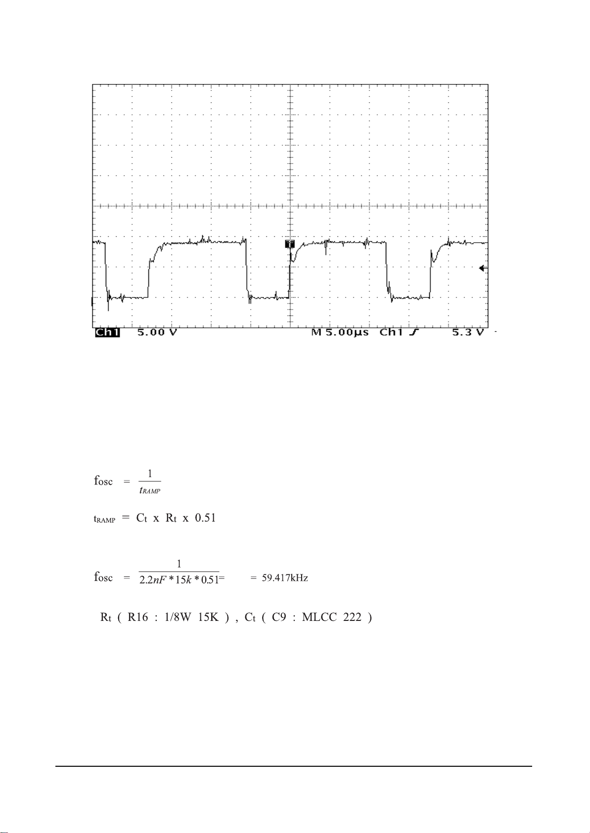
(1) AC-DC Converter
The Power supply output +400V DC from the common AC power supply using the active PFC
booster converter. This converter is designed for improving the power factor and preventing the
noise with high frequency and finally becomes the input power system for the switching regulator on the output side.
Picture1. PFC Drive FET(2SK2372) Drain pulse
Page 4
Circuit Operation Description
5-4 Samsung Electronics
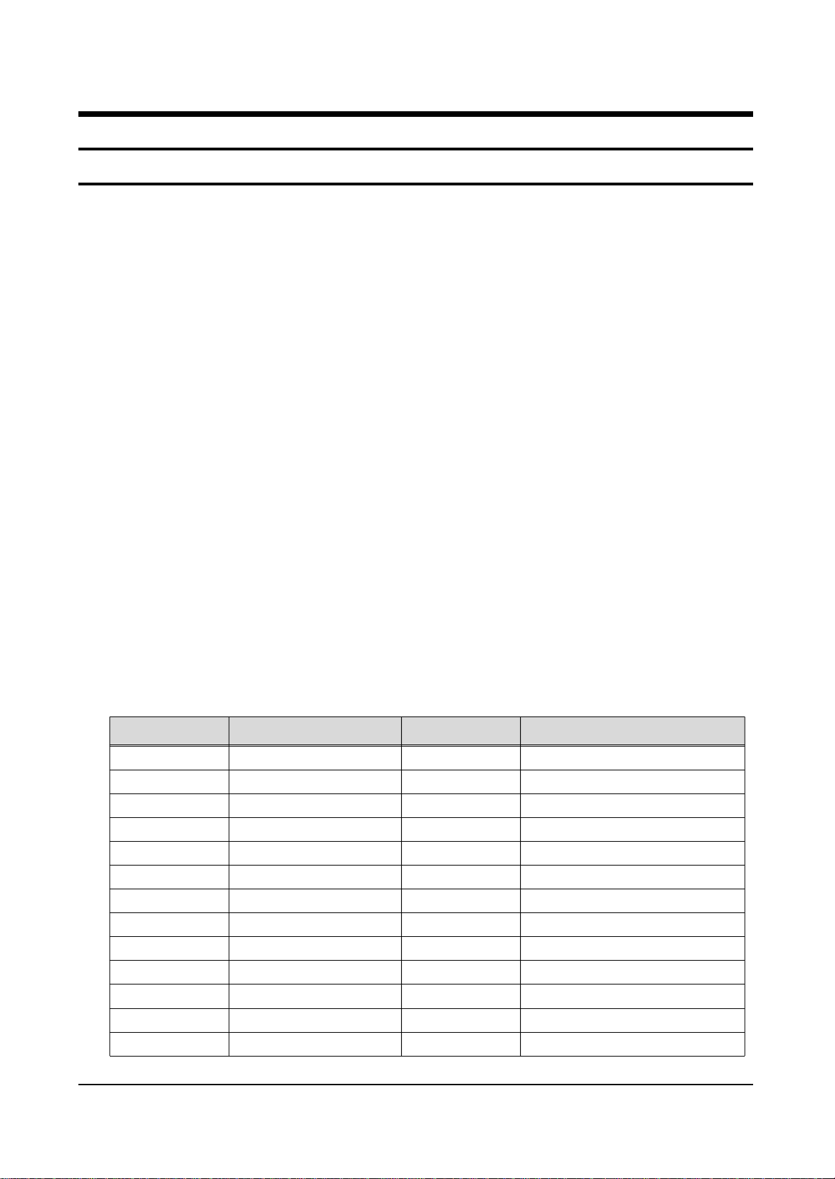
- Oscillator Frequency
Oscillator Frequency is determined by the values of Rt and Ct, which determine the ramp and
off-time of the oscillator output clock
Oscillator Frequency is derived from the following equation
For the circuit shown in the PDP50, with the oscillator running at
Picture2. PFC Drive FET(2SK2372) Gate pulse
Page 5
Circuit Operation Description
Samsung Electronics 5-5
(2) AC-DC Converter
Auxiliary Power Supply
The auxiliary power supply is a block generated power of micom for remote controlling. Once
the power plug is inserted, this block always comes into operation, causing micom to get into the
standby state for the output. Thus, this output is called the standby voltage. And with the relay
ON signal inputted through the remote controller, this block turns the mechanical switch of relay
to ON for driving the main power supply.
Picture3. Standby flyback Pulse.
Page 6
Circuit Operation Description
5-6 Samsung Electronics
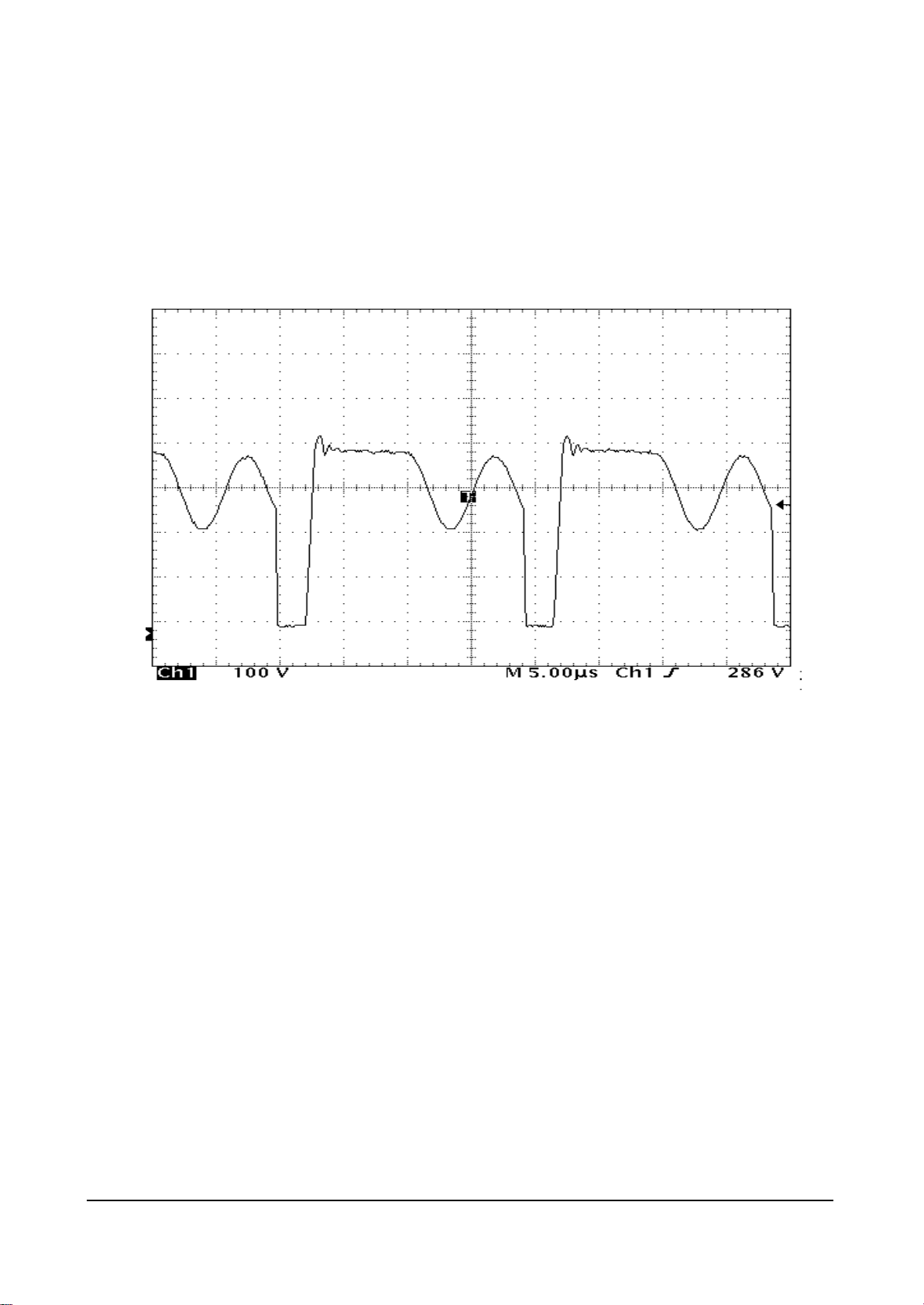
(3) Implementation of Sustain Voltage
As the main part of a SMPS for PDP, sustain voltage must supply a high power, 180V/1.8A.
To comply with the specification, the forward method was basically used. At the output stage two
90V converters are connected serially for high efficiency and reduction of system size against a
single 180V converter.
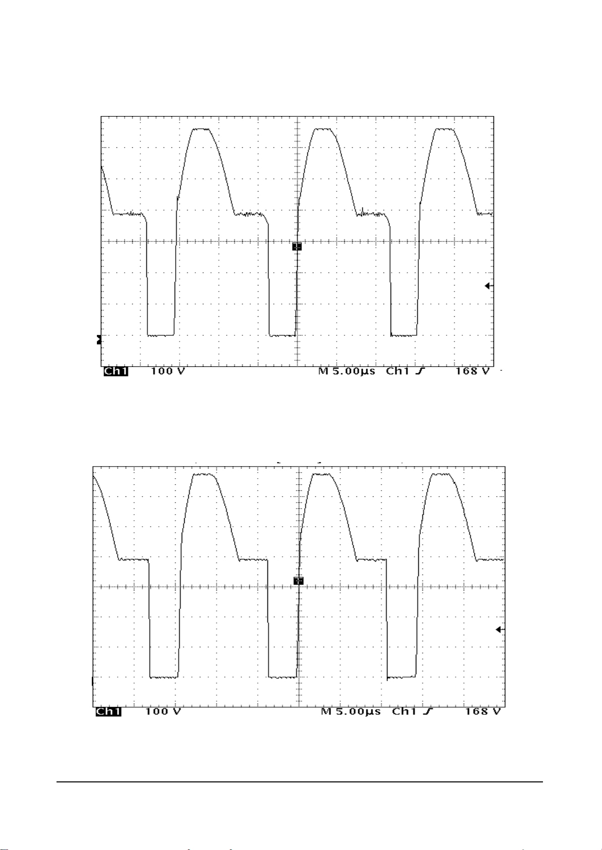
Picture4. VS Driving FET(2SK2968) drain pulse.
Picture5. VS Driving FET(2SK2968) gate pulse.
Page 7

Circuit Operation Description
Samsung Electronics 5-7
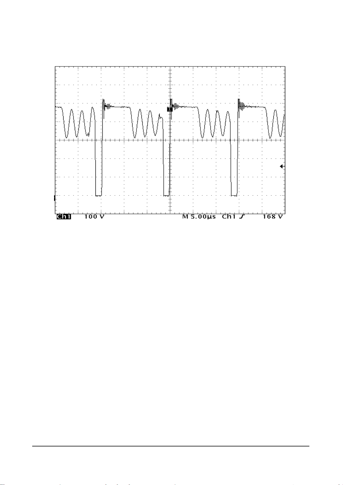
❏ PWM SECTION ( Pulse Width Modulator )
PDP SMPS use PWM IC ( KA3844 ) in PWM section. KA3844 is fixed frequency current-mode
PWM controller. They are specially designed for Off-Line and DC-to-DC converter applications
with minimum external components. These integrated circuits featurea trimmed oscillator for
precise dutycycle control, a temperature compensated reference, high gain error amplifier.
Current sensing comparator, and a high current totempole output Ideally suited for driving a
power MOSFET. Protection circuity Includes built in under -voltage lockout and current limiting.
This IC can operate with 50% duty cycle.
Picture6. KA3844 Oscillating Frequency pulse.
Oscillator timing capacitor (Ct) is charged by Vref through Rt and discharged by an internal
current source. During the discharge time, the internal clock signal blanks the output to the low
state. Selection of Rt and Ct therefore determines both oscillator frequency and maximum duty
cycle. Charge and discharge times are determined by the formula.
Page 8

Circuit Operation Description
5-8 Samsung Electronics
(4) DC-DC Converter
Input of VSCAN, VSET, VE is Sustain Voltage. This circuit use MA2820.
Maximum output wattage of MA2820 is 60W.
Picture7. MA series Block Diagram
Picture8. MA2820 main pulse.
Page 9
Circuit Operation Description
Samsung Electronics 5-9
(5) Output (VA,5V,12VSAMP) Pulse
Picture9. VA main pulse.
Picture10. 5V main pulse.
Page 10
Circuit Operation Description
5-10 Samsung Electronics
Picture11. 12VSAMP main pulse.
Page 11

Circuit Operation Description
Samsung Electronics 5-11
5-1-3 Block Diagram
Picture9. VA main pulse.
Page 12

Circuit Operation Description
5-12 Samsung Electronics
5-1-4 Connector Pin Assignment
NO
1
2
3
4
5
6
7
8
9
10
11
12
13
OUTPUT
+5.3V
SYM
VSB
User specification
RELAY
(INPUT)
5V/0.3A
MAX
User specification
NO
1
2
3
4
5
6
7
8
9
10
11
12
13
OUTPUT
+5.3V
GND
+18.3V
GND
80V
GND
205V
N.C
GND
GND
163V
163V
163V
SYM
Vcc
Vdd
Vscan
Vset
Vs
Vs
Vs
OUTPUT
+5.3V
GND
+18.3V
GND
190V
GND
80V
GND
GND
163V
163V
163V
SYM
Vcc
Vdd
Ve
Vscan
Vs
Vs
Vs
NO
1
2
3
4
5
6
7
8
9
10
11
12
NO
1
2
3
4
5
6
7
8
9
OUTPUT
+6.0V
GND(A)
+9V
+12V
GND(A)
+12V
+12V
GND(AMP)
GND(AMP)
SYM
+6V(A)
V9
V12
VSAMP
VSAMP
NO
1
2
3
4
OUTPUT
+5.3V
GND(D)
+5.3V
GND(D)
SYM
Vcc
Vcc
SA(Image Board) SY(Drive) SX(Drive)
Speaker SL(Logic)
NO
1
2
3
OUTPUT
AC
AC
AC
SYM
-
-
-
NO
1
2
3
OUTPUT
+12V
GND
SYM
VFAN
AC(INPUT) FAN(4EA)
NO
1
2
3
4
OUTPUT
+70V
+70V
GND
GND
SYM
Va
Va
BUFFER
FAN SIGNAL
Page 13

Circuit Operation Description
Samsung Electronics 5-13
5-1-5 Power Supply Systematic Diagram & Wiring Diagram
355
Xboard
Buffer
55
PDP 50Inch
PSA- 521B(
330
PSPD521901A
(
Logic Boar d
YBoard
INLET
FAN
Image Board
Spea ke r
Page 14

Circuit Operation Description
5-14 Samsung Electronics
5-1-6 Power Supply Layout
T306
BUFFER
VSET
H/S 1
SX
SY
SL
SPEAKER
T307
T308
VE
VSCAN
H/S 5
T303
T305
VA
12V
SAMP
H/S 6
T301
T301
VS
H/S 7
XF(FAN)1
X
F(FAN)2
X
F(FAN)3
X
F(FAN)4
X
F(FAN)5
S
A
H/S 4
T101
T304
5VSB
5V(D) , 12V
6V(A) , VG
9V
H/S 3
H/S 2
AC
INPUT
Pri mary
Secondary
Page 15

Circuit Operation Description
Samsung Electronics 5-15
5-2 Drive Circuit
5-2-1 Drive Circuit Overview
5-2-1(A) WHAT IS THE DRIVER CIRCUIT
It is a circuit generating an appropriate pulse (High voltage pulse) and then driving the panel to
implement images in the external terminals (X electrode group, Y electrode group and address electrode), and this high voltage switching pulse is generated by a combination of MOSFETs.
5-1-2(B) PANEL DRIVING PRINCIPLES AND TYPES OF DISCHARGE BY DRIVE PULSE
In PDP, images are implemented by impressing voltage on the X electrode, Y electrode and address
electrode, components of each pixel on the panel, under appropriate conditions. Currently, ADS
(Address & Display Separate: Driving is made by separating address and sustaining sections) is
most widely used to generate the drive pulse. Discharges conducted within PDP pixels using this
method can largely be
classified into 3 types, as follows:
① Address discharge: This functions to generate wall voltage within pixels to be lighted by
addressing information to them (i.e., impressing data voltage)
➁ Sustaining discharge: This means a display section where only pixels with wall voltage by the
address discharge display self-sustaining discharge by the support of such wall voltage.
(Optic outputs realizing images are generated.)
➂ Ramp reset discharge: To have address discharge occur selectively in pixels, all pixels in the panel
must have the same conditions (i.e., the same state of wall and space electric discharges).
The ramp reset discharge section, therefore, is important to secure the drive margin, and methods
most widely used to date include wall voltage controlling by ramp pulse.
Page 16

Circuit Operation Description
5-16 Samsung Electronics
5-1-2(C) Discharge of Drive
① Sustaining discharge
1(C). Kinds and detailed descriptions of driving discharge
Sustaining discharge means a self-sustaining discharge generated by the total of the sustaining
pulse voltage (usually, 160~180V) alternately given to X and Y electrodes during the sustaining
period and the wall voltage which varies depending upon pixels' previous discharge status. It is
operated by the memory function (through this, the current status is defined by previous operation conditions) AC PDP basically possesses. That is, when there is existing wall voltage in pixels
(in other words, when pixels remain ON), the total of wall voltage and a sustaining voltage to be
impressed subsequently impresses a voltage equal to or above the discharge start voltage, thereby
generating discharge again, but when there is no existing wall voltage in pixels (in other words,
when pixels remain OFF), the sustaining voltage only does not reach the discharge start voltage,
thus causing no discharge. The sustaining discharge is a section generating actual optic outputs
used in displaying images.
➁ Address discharge
This means a discharge type generated by the difference between positive voltage of the address
electrode (usually, 60~70V) and GND of the Y electrode. The address discharge serves to generate
wall voltage in pixels where images are to be displayed (that is, discharge is to be generated) prior
to the sustaining discharge section. Namely, pixels with wall voltage by the address discharge will
generate sustaining discharge by the following sustaining pulses.
➂ Weak erasing discharge
The purpose of resetting discharge is to make even wall voltage in all pixels on the panel.
Wall voltage which may vary depending upon the previous sustaining discharge status must be
made even. That is, wall voltage generated by the sustaining discharge must surely be removed,
by making discharges and then supplying ions or electrons. Wall voltage can be removed by making discharges and then setting a limitation on time for opposite polarity charging of the wall voltage or generating weak discharge (Low voltage erasing) to supply an appropriate quantity of ions
or
electrons and keep polarities from being charged oppositely. The weak discharge (Low voltage
erasing) methods which have been known to date can largely be into two types:
1) the log pulse adopted by most companies including F Company, and
2) the ramp pulse adopted by Matsushita.
In both two methods, impression is made with a slow rising slope of the erasing pulse. Because
the total of the existing wall voltage and a voltage on the rising pulse must be at least the drive
start voltage to generate discharges, external impressed voltage is adjusted based on the difference
in wall voltage between pixels.
And, weak discharge is generated because of a small impressed voltage.
Page 17

Circuit Operation Description
Samsung Electronics 5-17
5-1-2(D) Pulse of Reset, Address and Sustain period and optic output
Page 18

Circuit Operation Description
5-18 Samsung Electronics
5-2-2 Drive pulse and functions (ADS-driven method)
Page 19

Circuit Operation Description
Samsung Electronics 5-19
5-2-2(A) FUNCTIONS OF PULSES
① Narrow-width erasing pulse
X Narrow-width erasing pulse
Pulses in the sustaining section always begin with Y electrode pulse and end with X electrode
pulse.
Especially, the last of the X electrode has a narrow width, which serves as erasing discharge to
remove the wall electric charge on electrodes by setting a limitation on time for generating such
electric charge, as explained above. This method removes wall voltage on pixels which remained
ON in the sustaining section, thereby making even all pixels.
➁ Ramp rising pulse
The purpose of ramp rising pulse is to make wall voltage to some level for low voltage address
drive (includig low level sustain) in all pixels on the panel.
➂ Ramp falling pulse and X Ve level
Ramp falling pulse and Ve pulse are using to keep the wall charges safely which were generater
by ramp rising pulse to next steps
➃ scan pulse
This is called the scan pulse, selecting each of Y electrodes on a one-line-at-a-time basis. In this
case, Vscan means the scan bias voltage, functioning to lower switching voltage of the drive IC
(by switching Vscan into ground). Ground is impressed on electrode lines with ground impressed
on, and 75V (Vscac) is impressed on other lines, so that only pixels with data voltage (usually,
65V) impressed on electrodes have the discharge start voltage (65V) or higher for address discharge. Thus, because scan pulse and data pulse are impressed line by line, very long time is taken
for PDP addressing.
➄ 1st sustaining pulse
The sustaining pulse always begins with the Y electrode. This is because when address discharge
[positive (+) voltage on ADD electrode and negative (-) voltage on Y electrode] is generated,
positive (+) wall voltage is generated on the Y electrodes. Because wall electric charge generated
by address discharge is generally smaller than wall voltage generated by sustaining discharge,
initial discharges have small discharge strength, and stabilization is usually obtained after 5~6
times discharges, subject to variations depending on the structure and environment of electrodes.
The purpose of impressing the initial sustaining pulses long is to obtain stable initial discharges
and generate wall electric charges as much as possible.
Page 20

Circuit Operation Description
5-20 Samsung Electronics
5-2-3 Configuration and operation principles of driver circuit
YA
YB
H
Y-Board
- Sustian pulse
- Energy recovery
- Reset ramp pulse
- Vscan pulse
13pin - 250mm
I
4pin
(SMPS - Y : 13pin - 510 mm)
LOGIC
( SMPS - Logic : 4 - 550 mm)
2pin
speaker(9pin
¿»(13pin)
Fan (3pin)
SMPS
AC line filter
Y(13pin)
Logic(4pin)
)
Ground Connection
J
(SMPS-ADDRESS : 4pin - 220mm)
( SMPS - X : 12pin - 210mm )
Addres(4pin)
)
X(12pin
(SMPS - - 550mm)
12pin - 250mm
X-Board
-Sustain pulse
-Energy recovery
ADDRESS : 4pin
12pin - 200mm
13pin - 200mm
4pin power
E
F
(Logic - X : 13 + 12- 800mm)
G
4pin power
Page 21

Circuit Operation Description
Samsung Electronics 5-21
5-2-3(A) DESCRIPTIONS OF EACH BOARD'S FUNCTIONS
① X-Bd
Main PCB
Connected to the panel's X terminal, generating sustaining voltage pulse (including ERC), and
whole erasing pulse.
➁ Y-Bd
Main PCB
Connected to the panel's Y terminal, generating sustaining voltage pulse (including ERC), and log
erasing pulse.
➂ Y-buffer
Upper part + lower part
Board impressing scan pulse on Y terminals, consisting of the upper and lower sub-boards.
With wide VGA, one board is equipped with 4 scan driver ICs (SN755858: 64 outputs).
➃ COF
Upper part + lower part
Impresses Va pulse on address electrodes in the address section and generates address discharge
based on a difference between such Va pulse and scan pulse impressed on Y electrodes.
Page 22

Circuit Operation Description
5-22 Samsung Electronics
5-2-3(B) DRIVING BOARD'S BLOCK DIAGRAM
❏ Components of driving board's operations
1. Power supply
(1) Supplied from the power supply board
- For sustaining discharge: 155V ~ 170V
- For Ramp rising voltage,Vset: 200V ~ 235V
- For X Ve level: 185V ~ 195V
- For scan: 85V;
- For addressing discharge: 63V ~ 73V
- For logic signaling buffer: 5V
- For gate driver IC: 15V.
2. Logic signal
(1) Supplied from the logic board
- Gate signals for FETs.
LOGIC SIGNAL INPUT
LOGIC SIGNAL BUFFER
FET GAT E DRIVER
REC O V ERY
SWITC HING
RECOVERY C IRC UIT
(Recovery Cap)
MAIN
S WITCHING
165V
5V
18V
VSET
S WITCHING
POWER
205V 190V
VE
SWIT CHING
80V
VSCAN
S WITCHING
Page 23

Circuit Operation Description
Samsung Electronics 5-23
5-2-3(C) PRINCIPLES OF FET'S OPERATION AND HIGH VOLTAGE SWITCHING
❏ FET’s operation principles
❏ FET’s high voltage switching principles
(1) With signal impressed on the gate(Positive voltage), FET
gets short-circuited (a conducting wire of zero (0) resistance); and
(2) With no signal impressed on the gate (GND), FET gets
open-circuited (a non-conducting wire of ∞ resistance).
(1) With signal impressed on the gate(Positive
voltage), FET gets short-circuited (a conducting wire of zero (0) resistance); and
(2) With no signal impressed on the gate
(GND), FET gets open-circuited (a non-conducting wire of ∞ resistance).
Page 24

Circuit Operation Description
5-24 Samsung Electronics
5-2-3(D) DRIVER CIRCUIT DIAGRAM
Cp
2
1
3 2
1
3
Vs
Yr
D_YVsC
D_Yr
LY
C_Yerc D_YGC
D_Yf
Yf
0 0 00
Ys
Yg
Ramp
Rset
Dset
Cset
Yfr
Yrr
Ramp
Yp
+5V
D_fVdd
C_fVdd
VscanVset
C_Ysink
floating 5V
Ysc
Ysp
Dscan
D_Ysink
Ramp
Xrr
VsVe
C_Xsink
D_Xsink
Xs
Xg
0
D_Xs
LX
Xr
D_YVsC
D_Xr
C_Xerc
D_YGC
D_Xf
Xf
0 0
Page 25

Circuit Operation Description
Samsung Electronics 5-25
5-2-3(E) X BOARD TEST: ASSEMBLE LOGIC AND POWER INPUT JACK.
5-2-3(E)-1 Gate Signal Test
Condition) Connect 5V, GND, 17V to power connectors 1, 2, 3, respectively and then check each
TP shows like figures below.
① R4001 ② R4004
➂ R4015 ④ R4035
➄ R4031
Page 26

Circuit Operation Description
5-26 Samsung Electronics
5-2-3(E)-2 X Output Waveform Test
Condition) After applying 5V, 17V, 168V, 190V successively, use a probe to check #6 (connector),
and then check the following waveform shows at an oscilloscope.
➅ R4001
Page 27

Circuit Operation Description
Samsung Electronics 5-27
5-2-3(F) Y BOARD TEST: CONNECT A CABLE TO Y BUFFER AND ASSEMBLE A LOGIC AND POWER INPUT JACK.
5-2-3(F)-1 Gate Signal Test
Condition) Connect 5V, GND, 17V to Y power connectors 1, 2, 3, respectively and then check each
TP shows like figures below.
① R5029 ② R5052
➂ R5001 ④ R5083
➄ R5035 ➅ ZD5002
Page 28

Circuit Operation Description
5-28 Samsung Electronics
➆ M5014 ➇ M5037
⑨ R5077 ⑩ TPSI
1 TPPOL 2 TPBLK
Page 29

Circuit Operation Description
Samsung Electronics 5-29
5-2-3(F) Y BOARD TEST: CONNECT A CABLE TO Y BUFFER AND ASSEMBLE A LOGIC AND POWER INPUT JACK.
5-2-3(F)-2 Y Output Waveform Test
Condition) After applying 5V, 17V, 168V, 70V, 210V successively, use a probe to check #15
(TPOUT1), and then check the following waveform shows at an oscilloscope.
3 TPSTB 4 TPCLK
5 TPOUT1
Page 30

Circuit Operation Description
5-30 Samsung Electronics
5-3 Logic Part
5-3-1 Front Block
5-3-1(A) FRONT BLOCK DIAGRAM
Page 31

Circuit Operation Description
Samsung Electronics 5-31
5-3-2 The Description of the Logic Board
5-3-2(A) THE DESCRIPTION OF THE LOGIC BOARD
The logic board consists of the logic main board and the buffer board. The logic main board
processes the video signal, and generates the output address driver output signal, as well as XY
drive signal.
The buffer board stores the address driver output signal, and sends the signal to the address driver IC (COF module).
LOGIC BOARD
LOGIC MAIN
FUNCTION
-. Video signal processign (W/L, Error diffusion, APC)
-. Output address driver control adn data signal.
-. Outputs XY drive board control signal.
Sends data and control signals to three COFs at the left bottom part.
Sends data and control signals to five COFs at the middle bottom part.
Sends data and control signals to three COFs at the right bottom part.
Sends data and control signals to three COFs at the left top part.
Sends data and control signals to three COFs at the middle top part.
Sends data and control signals to three COFs at the right top part.
LOGIC
BUFFER
BOARD
E Buffer Board
F Buffer Board
G Buffer Board
H Buffer Board
I Buffer Board
J Buffer Board
Page 32

Circuit Operation Description
5-32 Samsung Electronics
NO
1
2
3
4
5
6
7
8
9
10
NAME
LVDS Connector
Operation LED
Key Scan Connector
24C16(128APC)
Y Connector
X Connector
LE01, LE02 and LE03
(Address Buffer Connector)
LG01, LG02 and LG03
(Address Buffer Connector)
Power Fuse
Power Connector
FUNCTION
An input connector that receives LVDS encoded RGB, H, V DATAEN and
DCLK signals from the video board.
Indicates if the logic board properly receives Sync and clock signal.
In normal state, it flickers every on second.
A connector that connects to the Key Scan board in order to check and
adjust 24C16 data.
An EEPROM for saving the gamma table, the APC table, the drive signal
timing and other options.
A connector that connects to the output address data, and control signals
to the E F and G buffer board.
A connector that connects to the output address data, and control signals
to the E F and G buffer board.
A fuse connector to the power source(5V) line of the logic board.
A connector to supply power(5V) to the logic board.
A connector that connects to the Y output drive board control signal.
A connector that connects to the X output drive board control signal.
5-3-2(B) THE NAME AND DESCRIPTION OF THE MAJOR COMPONENTS OF THE LOGIC BOARD
Page 33

1. External/Internal Input Mode Selection Features of 50”HD Multi Logic
Input selection features are provided. The Dip Switch and Logic circuits are designed to allow inspection
of NTSC and PAL internal patterns in the M3 module while in production or upon shipment.
External Mode Selection
1. When the NTSC mode is being selected, enter PAGE00/ When the PAL mode is being selected, enter
PAGE40.
2. Set the address value of Register 2E at 01.
3. Adjust the Dip Switch as shown in the above figure.
(UP : PIN_NUMBER 6,5,3,2,1 / DOWN : PIN_NUMBER 4)
Circuit Operation Description
Samsung Electronics 5-33
REGISTER
ADDRESS
2E
2E
PAGE
00
40
MODE
NTSC
PAL
EXTERNAL
MODE VALUE
01
01
DIP SWITCH STATE
EXTERNAL MODE
External Mode Selection
1. When the NTSC mode is being selected, enter PAGE00/ When the PAL mode is being selected, enter
PAGE40.
2. Set the address value of Register 2E at 00.
3. Adjust the Dip Switch as shown in the above figure.
(UP : PIN_NUMBER 6,5,4,3,2 / DOWN : PIN_NUMBER 1)
REGISTER
ADDRESS
2E
2E
PAGE
00
40
MODE
NTSC
PAL
EXTERNAL
MODE VALUE
00
00
DIP SWITCH STATE
EXTERNAL MODE
External Mode Selection
1. When the NTSC mode is being selected, enter PAGE00/ When the PAL mode is being selected, enter
PAGE40.
2. Set the address value of Register 2E at 00.
3. Adjust the Dip Switch as shown in the above figure.
(UP : PIN_NUMBER 6,5,4,2 / DOWN : PIN_NUMBER 3,1)
REGISTER
ADDRESS
2E
2E
PAGE
00
40
MODE
NTSC
PAL
EXTERNAL
MODE VALUE
00
00
DIP SWITCH STATE
EXTERNAL MODE
3456
2
1
6
4
5
3
2
1
6
4
5
3
2
1
Page 34

Circuit Operation Description
5-34 Samsung Electronics
LD2010
LD2002
LD2001
..
..
..
..
CN2000
..
..
..
..
..
..
..
..
U2050
F3
U2049
F2
EP20K400EBC652 - 1
LA2000
U2034
ALETRA
APEX
U2001
F1
TM
CN2001
U2048
67.4
X2007
U2033
1 40 1 40 1 40
LG2001 LG2002 LG2003
U2011~U2021
U2002
SAMSUNG
K4G323222A
U2005
SPLS - HMEM
SAMSUNG
K4G323222A
U2006
FU102
CN2002
1
LY1
40
FU2101
D2002
D2001
FU2102
L2004
L2005
U2040
U2041
50
REGIST
U2035
U2039
U2052
U2051
U2038
U2043 U2042 U2044
U2047
U2037
U2036
51.0
X2006
IC108
IC123
U2003
SPLS - HMEM
U2004
SPLS - HMEM
SAMSUNG
K4G323211A
U2007
SAMSUNG
K4G323222A
U2008
SAMSUNG
K4G323222A
U2009
SAMSUNG
K4G323222A
U2010
U2046
SW2000
U2045
CN2003
1 13 40 1 40 1 40 1
LE1 LE2 LE3
U2022~U2032
Page 35

Circuit Operation Description
Samsung Electronics 5-35
5-4 Scaler Board Block Diagram & Description
5-4-1 General Signal Process B/D
Mai n CVBS
S-Vi deo(Y/C)
Scar t Jac k
Component I nput Jac k
DVD YPbPr
( 480P, 480i )
Component I nput Jac k
DTV YPbPr
( 480P, 720P, 10800i )
PC I nput( 15Pi n D-s ub)
VGA To SXGA
( Hf : 31 TO 80KHz )
( Vf : 56 TO 75Hz)
480i
DVD-Y/ SCT_G
DVD- P b / SC T- B
DVD-P r /SCT _R
480P
9VA
SDA/SCL
DTV Y/Pb/ Pr
PC_R/ G/B, H/ V- SYNC
HD_PC_SW(PW364)
DDC I C
( 24LC21-I C506)
3D_Comb
Mai n CVBS
Mai n Y/ C
SCT_F B/SCT _CVBS
I VVS/ I VHS
Multi Component Pr ocess or
( CXA2101- I C402)
( YPbPr ➞ RGB)
R/ G/ B _OUT
HS_OUT 2 / V S_OUT 1
Analog Switc h
( BA7657F - I C501)
PC_DET
CAPT_CVBS
PC_V- SYNC
Main Vi deo Decoder
( VPC3230- I C201)
RESET Q
SDA/SCL
5V_A, 3. 3V_D
TTX_F B/ R/G/ B
V-YPbPr
HS/ V S_OUT 1
SCP
R/ G/ B _OUT
HS_OUT 1
AD_R_ OUT
AD_G_OUT
AD_B_ OUT
LLC1 : 13. 5MHz
CLK2 : 2 7MHz
Y/ UV 8Bi t
H1/ V 1_ OUT
CLK2 0
Sandcast l e Pul e Gen
(M4LV-32 - I C401)
3. 3VA
SDA/SCL
A/ D C on v e r t er Wi t h P L L / Ga i n Am p
VS_OUT1
A/ D C on v e r t er Wi t h P L L / Ga i n Am p
3. 3V_A
SEL_[ 0~2]
( AD9884 - I C801)
( AD9884 - I C101)
5V
VFI ELD
RESET Q
SDA/SCL
3. 3V_D
I nter l ace To Pr ogr ess i ve
( SDA9400 - I C202)
YI N/ UVI N[0~7]
3CH. DA Conver t er
( SDA9280 - I C703)
RESET Q
SDA/SCL
5V_A
EEPROM
( 24C16 - I C302)
SCL1 /SDA1
R/G/B [ 0~7]
VHS/VCL K
I VCL K/I VPEN
I VHS/ I VVS
SR[0~23]
SQ[ 0~23]
SOG/ M HS/ P CL K
CKI NV/ CL AMP
MHSYNC
MC OAST
RXD/T XD
MAX232- I C603
Ser i a l
Interface
M_RSTR
M_RE
M_OE
LLC1
Sub Video Decoder ( PI P)
Y_[0~7]
C[ 0~7]
I VVS
IVHS
( I CT003- 4S641632)
EEPROM
SDA/SCL
(PW364 - I C301)
FAN_DET
PC_DET
TH_DET
PROTECT
Megat ext SDA6000
SDRAM
CAPT_CVBS
( 24C16 - I C302)
Image Pr ocessor ( Image Scal i ng,
OSD Mi x e r , F r a me Ra t e
Conver si on With CPU)
MCKEXT: 130MHz
DCKEXT: 2 6MHz
OSC
MAIN_CVBS
MAIN_Y/C
D
VD_Pb/ SCT_B
DVD_Y/SCT_G
DVD_Pr /SCT _R
( VPC3230- I CP01)
Y[ 0~7]
C[ 0~7]
( 81V04160-I CP02)
SDA3/SCL 3
3. 3 V_D, 2. 5V_t t x
LEDRED/GRN
I RRCVR/ I RRCVR1
KEY[1~4]
R/ G/B 8 Bi t
LVS/ L HS/
LENG
A[1~19]
D[0~15]
ROMWEn
ROMOEn
A[0~18]
D[0~15]
RAMWEn
RAMOEn
BHENn
SCT_CVBS
SCT_F /B
RESET Q
SDA/SCL
3. 3V_D
5V_A
3. 3V_D
RESET Q
A[0~20]
D[0~15]
EPROM
( I CT002- M27V160)
I R Modul e
Ent ernal Keypad
LVDS( DS90C385 - I C503)
Fl ash Memory
29LV160 - OTP01
Sr am
616V1000 - I C602
Page 36

Circuit Operation Description
5-36 Samsung Electronics
5-4-2 Description in Signal Process Block
VPC3230 : This functions as a video decoder, which can receive all of the YC, YUV, CVBS inputs.
In addition, this converts Y/C into YUV after receiving 3D Comb Output Y/C, S-Vido Y/C, and DVD YUV.
VIDEO DOUBLER : Usually, the current video image adopts the INTERLACE Scanning system and it has poor video because of
Flicking on the screen. Using the SDA9400 , INTERLACE is converted into PROGRESSIVE in order to
improve the quality of video.
VIDEO PROCESSOR : Since the HD modes like 1920*1080I have higher video bandwidth than the existing video signals, the
ordinary decoder like VPC3230 can't handle those modes. PC has higher bandwidth of video signal than
TV and the RGB video format.
Therefore, if the HD signal can be converted into the RGB signals, the TV video signal can have the same
processing as the PC VIDEO signal. CXA2101 developed by SONY is used to convert YPbPr into RGB.
CXA2101 converts both DTV signals and all the SD signals processed in the sequence of SDA9400 then
SDA9280 into RGB.
This processor performs some user control functions, such as tint, color, and sharpness.
Also, it controls high light gains low light offsets when doing white balance adjustments.
ANALOG SWITCH : The video decoder like VPC3230 has a built-in video switch that assigns one signal out of various
received inputs, though most of ICs for PC are designed so that they support only one source because of
less necessity of simultaneously processing the multi inputs. To process the input source of MULTI
(PC&HD), therefore, a function of selecting an input should be externally added; as is performed by
ROHM's BA7657F. PW364 transmits a signal determining which input is selected.
ADC : A device that converts the input RGB signals into the 8bit DIGITAL RGB signals.
In case of white balance adjustments, this device sets the color temperature by controlling R/B gains and
R/B offsets.
PW364 : PW364 is a multi-functional scaler which one chip has video signal scaling, 8086 CPU, 4M BYTE VIDEO
MEMORY functions. The PC and Video input signals are received from GRAPHIC PORT and VIDEO PORT,
respectively.Its main functions include UP/DOWN SCALING, PIP, ZOOM, GAMMA CORRECTION,
Compensation of GEOMETRIC DISTORTION, powerful GRAPHIC OSD.
FIRMWARE : Mounted is a software that is used for system control by operating 8086 built in PW364. A 4MBIT FLASH
ROM is mainly used, but one up to 8MBIT can be used according to PROGRAM and capacity of OSD
DATA.
The system is easy to maintain because programming can be re-done at any yime using the FLASH ROM.
Page 37

Circuit Operation Description
Samsung Electronics 5-37
5-4 Main I/O signal pules and voltages
5-4-1 Signal Pulses of Image Board(Input Signal Conditions : 7 Color bar)
Page 38

Circuit Operation Description
5-38 Samsung Electronics
Page 39

Circuit Operation Description
Samsung Electronics 5-39
Page 40

Circuit Operation Description
5-40 Samsung Electronics
MEMO
 Loading...