

Page 1
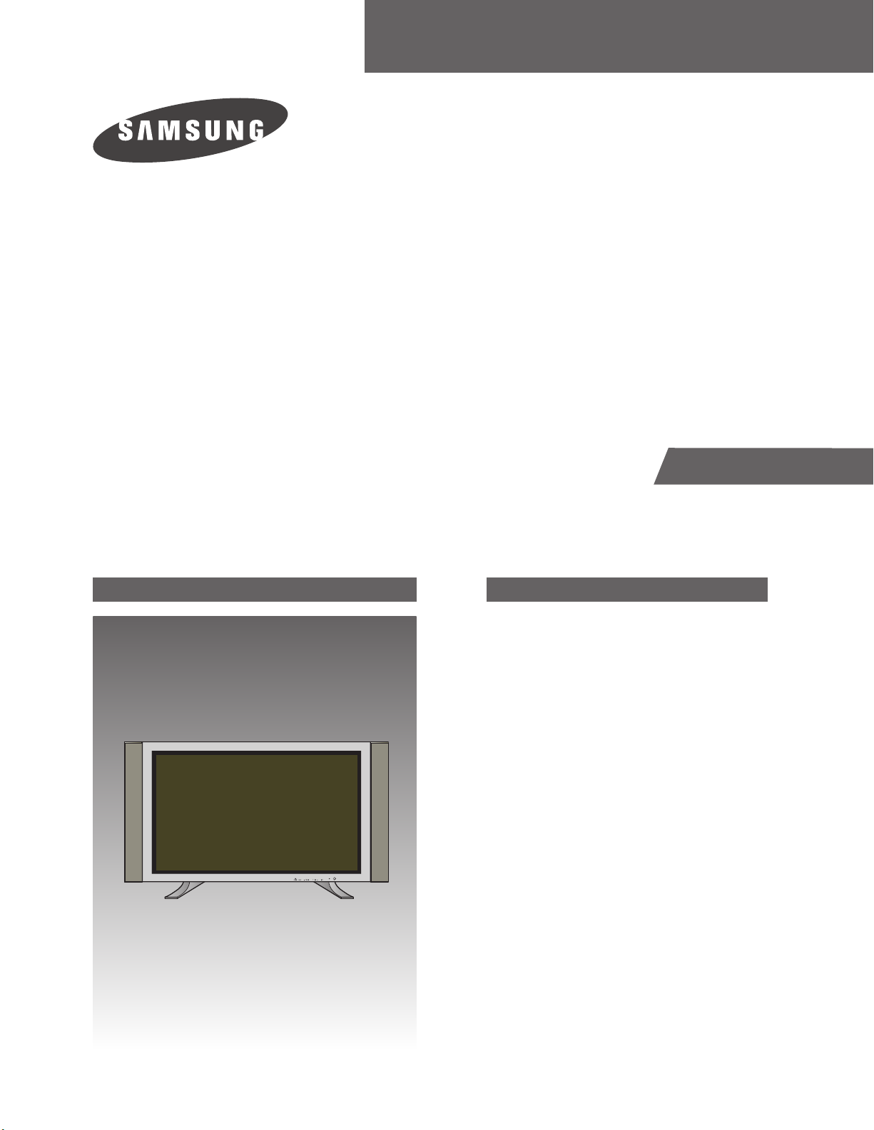
PLASMA DISPLAY TV
Chassis : D61B
Model: PPM42S3QX/XAA
PLASMA DISPLAY TV CONTENTS
Specifications
Alignment and Adjustments
Exploded View and Parts List
Electric Parts List
Schematic Diagrams
1.
2.
3.
4.
5.
SERVICE
Manual
Page 2
Specifications
Samsung Electronics 1-1
1. Specifications
MODEL
Display
Display
Screen Size
Voltage
Power Consumption
Number of Pixels
External Control
AUDIO Input
AUDIO Output
VIDEO Input
VIDEO Output
Dimensions
Weight
PPM42S3Q
1027(W) x 79(D) x 630.5(H) mm / 40.43(W) x 3.11(D) x 24.82(H) inches
31 Kg / 68.34 lbs (without stand)
107 Cm / 42 Inches
AC 120V, 60Hz / AC100-250V, 50/60Hz
330 Watts
852(H) X 480(V)
RS-232C IN(Mini jack), RS-232C OUT(D-SUB 9P)
VIDEO / S-VIDEO
COMPONENT 1
COMPONENT 2
RGB(PC) 1/2
DVI
External Speaker (10W+10W)
Audio Output (L/R RCA)
VIDEO
S-VIDEO
COMPONENT 1 - 480i / 480p / 720p / 1080i
COMPONENT 2/RGB2(PC) IN (BNC, 5P, 480i~1080i, VGA~XGA)
RGB1(PC1) - D-SUB 15P
DVI
Monitor Output (RCA)
Page 3

Alignment and Adjustments
Samsung Electronics 2-1
2. Alignment and Adjustments
2-1 Service Mode
2-1-1 SERVICE MODE Entry Method (General Transmitter)
■ For the General Transmitter
1. Turn the power off and set to stand-by mode.
2. Press the buttons of the transmitter in this order; Info-Menu-Mute-Power to turn the set on.
3. The set turns on and enters service mode.
* If you fail to enter service mode, repeat steps 1 and 2 above.
2-1-2 Initial DISPLAY State of SERVICE MODE
2-1-2(A) OSD DISPLAY
2-1-2(B) B
utton Operations in SERVICE MODE
1. VSP9437-1 9. CXA2101
2. VSP9437-2 10. LOSIC
3. FLI2300 11. TP LOG-ASI
4. ASI500-1 12. Option
5. ASI500-2 13. CheckSum 0000
6. DNIe 14. Reset
7. AD9888
8. CXA2151
Release : 2003-05-02 M_NNWS42M6_100
Menu
UP/DOWN Key
LEFT/RIGHT Key
Displays all menus
Cursor move to select items
Enable to increase and decrease the data of the selected items
SERVICE MAIN
Page 4
Alignment and Adjustments
2-2 Samsung Electronics
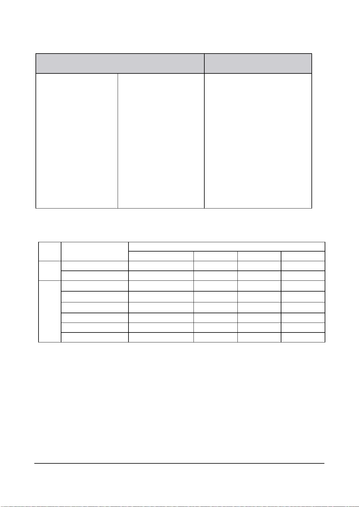
2-1-3 Factory Data Initial Value
VSP9437-1( Video) VSP9437-2( Video)
VPEAKING 16
H
PLL SPEED 00
RGB/YUV
RGB/YUV BR
YUV SATCB 25
YUV SATCR 28
PAL B/G 0 1
PAL D/K 01
PAL I 0 1
SE
CAMB/G 27
SE
CAMD/K 27
SE
CAML'/L 27
N
TSC M 01
N
TSC 4. 43 27
CONT36
IGHT244
ASI II500 DNIe
PI PRCONT 32
P
I PGCONT 32
P
I PBCONT 32
PAL 6 0 2 7
PAL M 0 1
PAL 0 1
SE
CAM27
N
TSC 01
N
TSC 4. 43 27
PAL 6 0 2 7
N
R 01
ideo/PC, DVI )
(V
BRIGHT OF FSET
CONTRA O
SCALE M
FFSET
AX Y 48
Attachment
Attachment
VPEAKING16
H
PLL SPEED 00
PAL 01
SE
CAM27
N
TSC 01
PAL AV 0 1
SE
CAMAV 27
NTSC AV 01
TH CORING02
PATT SEL 0 0
N
OISE TH3 100
P
I PRBRIGHT 00
P
I PGBRIGHT 00
P
I PBBRIGHT 00
P
I PFILTERIC 00
P
I PFILTER ML 00
P
I PFILTER MR 00
P
I PFILTER UC 00
SCALE
TH H
TH EDGE 0 4/ 05
N
CE U
CE CUT
CE G
D
SKI N ON 00
CTI GAI
D
MIN Y 16
PF00
R SEL 02
PPER 220/ 240
OFF 45
AIN64/75
CE GAIN 75/96
N 08
E NOISEGAIN08/10
HCO
NT 32
VCO
NT 32
B
LACK GAIN375
W
HITE GAIN 37 5
W
TE GAIN 30 0
CTE GAI
HS
VS
SHAR
C
H
N 176
HARP GAIN48
HARP GAIN48
PNESS 100
LKDLY 07
POSI 14
Page 5
Alignment and Adjustments
Samsung Electronics 2-3
F LI 2300 ASI I5 00 ( Vi deo/PC, DV I )
YDELAY 05
CDELAY 12
CONTRAST 90
BRI GHTNESS 160
SATURATION 110
AD988 8
Vi deo/Comp/PC
R GAI N 71/ 128/ 83
R CONTRAST 32/ 30
G CONTRAST 32/ 30
B CONTRAST 32/ 30
RBRIGHTNESS 00
GBRIGHTNESS 00
BBRIGHTNESS 00
TE XT ALPHA 01
TEXT T HRESHOLD 07
FILTER ML 00
FILTER MR 00
FILTER F R 00
FILTER MC 16
FILTER UC 00
FILTER L C 00
CXA210 1
(Video,COMP)
PICTURE 20
FI L TER YPASS 00
RGAMMA 32
GGAMMA 32
BGAMMA 32
HPOSITION 00
VPOSITION 00
HSIZE 00
VSIZE 00
OVERSCAN R 50
OVERSCAN G 50
OVERSCAN B 50
SUB BRIGHT 32
G GAI N 77/122/ 81
B GAI N 95/ 128/ 81
ROFFSET 63/79/64
GOFFSET 66/53/70
BOFFSET 64/82/68
V- PATH PC
AUTO COLOR OFF
HUE 34
COLOR 19
BRIGHT 61
SHARPNESS 16
RDRIVE 04
GDRIVE 04
BDRIVE 04
RCUTOFF 32
GCUTOFF 32
BCUTOFF 32
CR OFFSET1 07
CB OFFSET1 07
SUB CONT 08
SUB COL 10
SUB HUE 08
R- Y/R 13
R- Y/B 15
G- Y/ R 13
G- Y/ B 02
Page 6
Alignment and Adjustments
2-4 Samsung Electronics
■ Attachment
Attachment
RDRIVE
GDR
IVE
BDR
IVE
RCUTOFF
GCUTOFF
BCUTOFF
G
AMMA 01
G
TS SET 01
ERD
MODE 02
RAN
DOM NOISE 00
D
IFF FILTER 01
A
PC 01
A
PC SET 00
A
PC VALUE 127
Attachment
Attachment
Attachment
Attachment
Attachment
(PD
LOGIC
P DRIVER)
ACTIVEVPOS 12
A
CTIVE HPOS 19
V
SYNC POS 03
H
SYNC POS 32
V
SYNC WIDTH 02
H
SYNC WIDTH 12
TP L OG-ASI
(TEST PAT LOGIC/SCA LER)
LOG PATTERN00
LOG H
IGH LEVEL 00
LOG L OW
A
SI COLORBAR 00
LEVEL 00
IC
DNIe
Logic
Contrast 54 48 50 55
R Cuto ff 131 116 125 123
G C utoff 130 127 128 128
B Cuto ff 137 124 152 136
W/B D ata
ITEM
Bright 41 58 43 36
R Gain 149 145 153 145
G Gain 130 130 130 130
B Gain 125 119 113 117
Video,S- V HS Component PC DVI
Page 7
Alignment and Adjustments
Samsung Electronics 2-5
Alignment and Adjustments
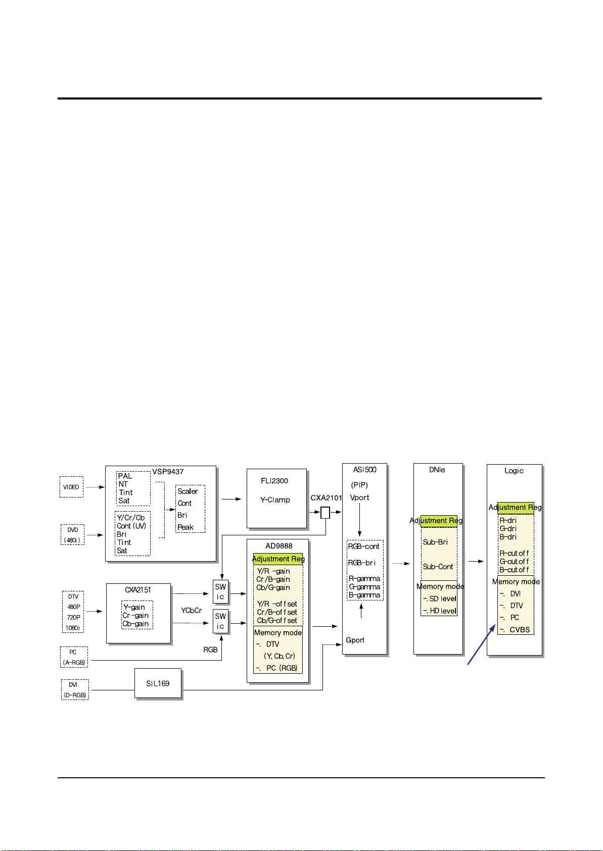
2-2 WHITE Balance Coordinates
2-2-1 White Balance Adjustment
1. W/B Adjustment is required for the following four modes: DVI → DTV → PC → CVBS(VIDEO)
→ CVBS(VIDEO PIP)
2. Adjustment Method (DVI, DTV, PC : VG828, CVBS : Adjust RF signals to match the
Toshiba pattern (in-house signal)
! Adjust the target set by adjusting the panel logic and the video DNIe adjustment register in
register in order to determine the referential W/B of the panel with a DVI input, which
is the full digital path.
@ For DTV adjustment, adjust the adjustment register of ad9888 to align the DTV signal
to the DNIe and logic panel value which was fixed with a DVI adjustment so that they are
in effect considered to be the same signals. (At this time, do not adjust the gain of
AD9888
→ the Highlight W/B does not need to be adjusted since its deviation falls
within valid distribution range.)
# PC adjustment is same as DTV adjustment. (The offset can be applied to the values
obtained through DTV adjustment. However, additional adjustment is required for
Y, Cb, and Cr of DTV since PC processes R, G, and B signals.)
$ cvbs adjustment is performed with the Toshiba pattern (in-house signal) and differs
from the VG828 signals in the above three modes. Hence, it should be performed with
the same method of ! DVI adjustment.
% Finally, activate PIP in video mode, and repeat W/B adjustment.
❈ Thus, Micom saves the W/B data separately for each memory mode of the block
(See the block diagram given below) during W/B adjustment.
Micom can memorize the four modes
separately. However, under the current
adjustment guidelines, DTV and PC are
memorized with the same value during
DVI adjustment and CVBS is memorized
with a separate value.
Page 8
Alignment and Adjustments
2-6 Samsung Electronics
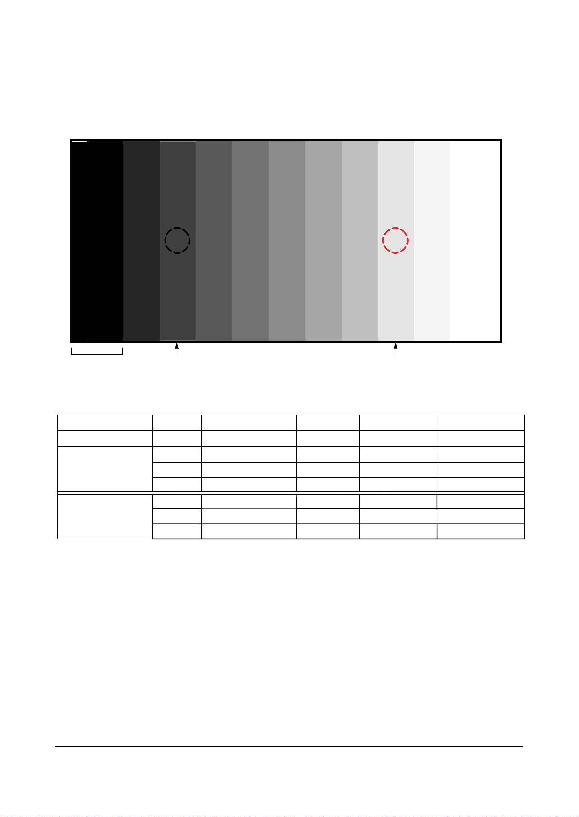
2-2-2 White Balance Coordinates by Mode
PedestalLevel Low Light
measure point
Video,S- VHS Component PC DVI
Tim ing 925LTH PAL- B 720p 640*480 60Hz 640*480 60Hz
x 275 280 280 280
H/L
L/L
y 280 287 295 295
Y(fL) 35 34 30 30
x 278 280 285 285
y 285 287 295 295
Y(fL) 1.3 0.6 0.8 0.8
High Light
measure point
Page 9
Alignment and Adjustments
Samsung Electronics 2-7
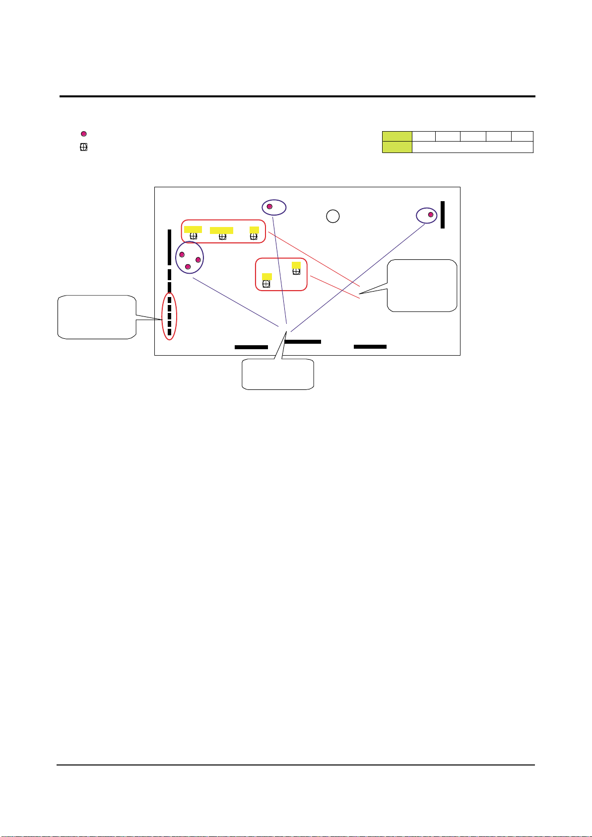
2-3 Voltage Adjustment
Test Point
VR : Variable Resisto r
Not us e d by t his Mode l
Common use with Other
Mode ls SMPS .
Fan power source.
VSET
VSCAN
VA
CN811
CN807
CN808
CN809
CN810
VSCAN
VSET
Output Va Vsc Vs Ve Vs e t
Voltage
Vs
9
VE
See the labels attached on the bas e c hassis
VE
SMPS
VS
VA
Validate the SMP S
voltage
Notes
☞
-. When the SMPS-PCB is replaced. the VA,VSCAN,VS,VE and VSET voltages
must be checked and adjusted to the proper to levels indicated on the panel sticker.
Adjust the SMPS
voltage using the
VR(Variable Re s i
stor)
Page 10

Electrical Parts List
Samsung Electronics 4-1
4-1 ASSY BOARD & PARTS LIST FOR SERVICE
4 Electrical Parts List
No
-
①
②
③
④
⑤
⑥
⑦
⑧
⑨
⑩
⑪
Description
ASSY PDP PANEL
ASSY PCB X MAIN
ASSY PCB Y MAIN
ASSY PCB LOGIC MAIN
ASSY PCB BUFFER(up)
ASSY PCB BUFFER(down)
ASSY PCB BUFFER(E)
ASSY PCB BUFFER(F)
ASSY PCB BUFFER(G)
ASSY PCB SMPS
ASSY PCB MISC DIGITAL
ASSY PCB MISC ANALOG
Code No
BN96-01209A
BN96-00870A
BN96-01211A
BN96-01212A
BN96-00872A
BN96-00873A
BN96-01213A
BN96-01214A
BN96-01215A
BN96-01217A
BN94-00536A
BN94-00536B
Specification
M3,S42D-YD,V3,42INCH,SEMCO SMPS,D65A,V3.1
M3,S42SD-YD,D65A,X MAIN BOARD,LJ92-00758A,V3
M3,S42SD-YD,V3,42INCH,V3.1,SDI CODE,LJ92-00944B
M3,S42SD-YD,V3,42INCH,V3.1,SDI CODE,LJ92-00975C
M3,S42SD-YD,D65A, Y BUFFER(UP) LJ92-00796A,V3
M3,S42SD-YD,D65A, Y BUFFER LJ92-00797A,V3
M3,S42SD-YD,V3,42INCH,V3.1,SDI CODE,LJ92-00811A
M3,S42SD-YD,V3,42INCH,V3.1,SDI CODE,LJ92-00812A
M3,S42SD-YD,V3,42INCH,V3.1,SDI CODE,LJ92-00813A
SPP4231,PS42D4S,110~240V
PPM42S3Q.D61B,NEWTON 2
PPM42S3Q.D61B,NEWTON 2
Page 11

Electrical Parts List
4-2 Samsung Electronics
4-2 SERVICE ITEM
You can search for the updated part code through ITSELF web site.
URL : http://itself.sec.samsung.co.kr
T0077 3903-000085 CBF-POWER CORD;DT,US,BP3/YES,I(IEC C13/C 1
M0114 AA39-00311A CBF SIGNAL;PDP,9P/1P,UL2851#28,5000MM,UL 1
M0114 BN39-00115A CBF SIGNAL;NL5MO,15P/15P,2990,1830MM,UL2 1
T0074 BN59-00366A REMOCON;TM76,D61A,42,G6148,PPM42S3,EX 1
T0098 BN94-00494L ASSY PCB MISC-CONTROL;SPD-42A4H,D55A,ALE 1
T0132 BN94-00536C ASSY PCB MISC-DIGITAL;PPM42S3Q,D61B,42P3 1
T0145 BN94-00536B ASSY PCB MISC-ANALOG;PPM42S3Q,D61B,NEWTO 1
M0003 BN96-00135K ASSY COVER P-FRONT;42P3S(VMB),SEA,HIPS V 1
T0001 BN96-00314C ASSY COVER P-BACK;PS42P3S,AL5052 T1.2,DG 1
T0532 BN96-00676A ASSY MISC P-FAN;PPM42S3 2
M0764 BN96-00756A ASSY STAND P-SCREW;PPM50H3,SCREW+PE-BAG, 1
T0073 BN96-00870A ASSY PDP P-X MAIN BOARD;M3,S42SD-YD,D65A 1
T0091 BN96-00872A ASSY PDP P-Y BUFFER (UP);M3,S42SD-YD,D65 1
T0092 BN96-00873A ASSY PDP P-Y BUFFER (DOWN);M3,S42SD-YD,D 1
T0044 BN96-01209A ASSY PDP P-MODULE;M3,S42SD-YD,V3,42INCH, 1
T0096 BN96-01211A ASSY PDP P-Y MAIN BOARD;M3,S42SD-YD,V3,4 1
T0172 AA69-02609A BAND-PP;W18,CLEA,1G 7.6 S.N.A
T0113 BN96-01213A ASSY PDP P-E BUFFER BOARD;M3,S42SD-YD,V3 1
T0114 BN96-01214A ASSY PDP P-F BUFFER BOARD;M3,S42SD-YD,V3 1
T0033 BN96-01215A ASSY PDP P-G BUFFER BOARD;M3,S42SD-YD,V3 1
T0764 BN96-01217A ASSY MISC P-SMPS;SPP4231,PS42D4S,110~240 1
Loc. Code No Description;Specification Q’ty S.N.A
4-2-1 PPM42S3QX/XAA
Page 12

Exploded View & Parts List
Samsung Electronics 3-1
3. Exploded View & Parts List
3-1 PPM42S3QX/XAA
No Code No Description;Specification Q’ty S.N.A
M0003 BN96-00135K ASSY COVER P-FRONT;42P3S(VMB),SEA,HIPS V 1
T0003 BN64-00071G CABINET FRONT;42P3 VMB,HIPS,V0,HF-1690H, 1 S.N.A
T0057 BP64-00177A BADGE-BRAND;ALL,AL,T1.5,70,11.3,BLK,SILI 1 S.N.A
T0022 BP64-00045C KNOB CONTROL;P3,ABS,HB,WP1000 1 S.N.A
T0061 BN64-00074B WINDOW-REMOTE;42P3S,PMMA,,,,,,CLEAR 1
T0098 BN94-00494L ASSY PCB MISC-CONTROL;SPD-42A4H,D55A,ALE 1
T0456 BN67-00128A GLASS-FILTER EMI;42V3,Sputter,44%,984*58 1 S.N.A
T0911 BN61-00244E BRACKET-FILTER TOP ASSY;42P3H,AL5052,1.2 1 S.N.A
T0912 BN61-00245H BRACKET-FILTER SIDE L;42P3S,AL5052,1.2 1 S.N.A
T0913 BN61-00309E BRACKET-FILTER SIDE R;42P3S,AL5052,1.2 1 S.N.A
T0914 BN61-00246E BRACKET-FILTER BOTTOM ASSY;42P3S,AL5052, 1 S.N.A
T0915 BN61-00141A HOLDER-MODULE;42P3,AL,DIECASTING 4 S.N.A
T0918 AA60-00110H SPACER-FILTER;42P3,P/U FROM,960,5,6 1 S.N.A
T0918 AA60-00110J SPACER-FILTER;50P3,P/U Form,20.0,2.0,5.0 2 S.N.A
T0044 BN96-01209A ASSY PDP P-MODULE;M3,S42SD-YD,V3,42INCH, 1
T0764 BN96-01217A ASSY MISC P-SMPS;SPP4231,PS42D4S,110~240 1
T0073 BN96-00870A ASSY PDP P-X MAIN BOARD;M3,S42SD-YD,D65A 1
T0096 BN96-01211A ASSY PDP P-Y MAIN BOARD;M3,S42SD-YD,V3,4 1
T0037 BN96-01212A ASSY PDP P-L MAIN BOARD;M3,S42SD-YD,V3,4 1
T0008 BN96-00313C ASSY COVER P-BACK SUB;42P3,DGM5233 T1.2 1 S.N.A
T0132 BN94-00536C ASSY PCB MISC-DIGITAL;PPM42S3Q,D61B,42P3 1
T0145 BN94-00536B ASSY PCB MISC-ANALOG;PPM42S3Q,D61B,NEWTO 1
T0001 BN96-00314C ASSY COVER P-BACK;PS42P3S,AL5052 T1.2,DG 1
T0112 BN63-00529B COVER-BACK;42P3,DGM5233,T1.2 1 S.N.A
T0916 BN61-00202B BRACKET-HANDLE;42P3,T1.5,DGM5233 2 S.N.A
T0555 BN96-00286F ASSY MISC P-BRACKET TERMINAL;P3,VMB 1 S.N.A
T0074 BN59-00366A REMOCON;TM76,D61A,42,G6148,PPM42S3,EX 1
T0268 3903-000085 CBF-POWER CORD;DT,US,BP3/YES,I(IEC C13/C 1
You can search for the updated part code through ITSELF web site.
URL : http://itself.sec.samsung.co.kr
T0268T0074
T0915
T0911
T0912
T0456
M0003
T0003
T0057
T0022
T0098
T0914
T0918
T0913
T0044
T0073
T0764
T0037
T0918
T0916
T0096
T0001
T0555
T0112
T0008
T0145
T0132
T0061
Page 13

Video/S-Video Sound
Video IN
Connector
COMPONENT1
S-Video
Analog - Digital Board
CXA2151Q
IC103
TP02
TP03
TP01
5. Schematic Diagrams
Samsung Electronics
Schematic Diagrams
5-1
5-1 ANALOG 1
TP01
TP02
TP03
This Document can not be used without Samsung’s authorization.
Page 14

Schematic Diagrams
5-2 Samsung Electronics
5-2 ANALOG 2
This Document can not be used without Samsung’s authorization.
3D COMB FILTER
To DC FAN
R246
TILT SENSOR
R247
FAN PART
50"
Page 15

Samsung Electronics
Schematic Diagrams
5-3
5-3 ANALOG 3
TP04
TP05
TP06
TP07
This Document can not be used without Samsung’s authorization.
TP05
TP04
From SMPS Board
TP06
MONITOR OUT VIDEO
TP07
MONITOR OUT SOUND
BD701
External Speaker
12
+12V_AMP
Page 16

5-4 ANALOG 4
Schematic Diagrams
5-4 Samsung Electronics
This Document can not be used without Samsung’s authorization.
74HCT573
74HCT573
Page 17

Samsung Electronics
Schematic Diagrams
5-5
5-5 CONTROL
This Document can not be used without Samsung’s authorization.
AA32-00013B
Page 18

Schematic Diagrams
5-6 Samsung Electronics
5-6 SMPS 1
This Document can not be used without Samsung’s authorization.
Page 19

Samsung Electronics
Schematic Diagrams
5-7
5-7 SMPS 2
Page 20

Schematic Diagrams
5-8 Samsung Electronics
5-8 SMPS 3
Page 21

Samsung Electronics
Schematic Diagrams
5-9
5-9 SMPS 4
Page 22

Schematic Diagrams
5-10 Samsung Electronics
5-10 DIGITAL 1
TP08
TP09
TP10
Analog - Digital board
Connector
TP08
42 SD
42 HD
50,63 HD
PC(D-SUB&DVI) SOUND
TP09
TP10
Page 23

Samsung Electronics
5-11
TP11
TP12
TP13
TP14
TP16
TP19
TP17
TP18
TP15
Schematic Diagrams
5-11 DIGITAL 2
TP11
TP12
TP13
TP14
TP15
TP16
TP17
TP18
TP19
This Document can not be used without Samsung’s authorization.
Page 24

5-12
Schematic Diagrams
Samsung Electronics
ANALOG EDID EPROM
BNC Connector
PC D-SUB
From SMPS board
TP23
TP22
TP20
TP21
TP24
5-12 DIGITAL 3
TP20
TP21
TP22
TP23
TP24
This Document can not be used without Samsung’s authorization.
Page 25

Samsung Electronics
Schematic Diagrams
5-13
USER EPROM (256K)
RS232C IN
Flash Memory
B12 : 1204-002105
From Remote Control board
RS232C OUT
TP25
TP26
5-13 DIGITAL 4
TP26
TP25
This Document can not be used without Samsung’s authorization.
Page 26

5-14
Schematic Diagrams
5-15
TP27
TP28
5-14 DIGITAL 5
TP28TP27
This Document can not be used without Samsung’s authorization.
Page 27

Schematic Diagrams
5-15
5-15
LVDS Connector
5-15 DIGITAL 6
This Document can not be used without Samsung’s authorization.
Page 28

5-16
Schematic Diagrams
Samsung Electronics
5-16 DIGITAL 7
This Document can not be used without Samsung’s authorization.
Page 29

Samsung Electronics
Schematic Diagrams
5-17
5-17 DIGITAL 8
This Document can not be used without Samsung’s authorization.
DVI Connector
DIGITAL EDID EPROM
 Loading...