

PLASMA DISPLAY TV
Chassis : D53A
Model: PPM42S2X/XAA
PLASMA DIAPLAY TV CONTENTS
Precautions
Reference Information
Specifications
Alignment and Adjustments
Circuit Operation Description
Troubleshooting
Exploded View and Parts List
Electric Parts List
Handling Description
Glossary
Wiring Diagram
Schematic Diagrams
1.
2.
3.
4.
5.
6.
7.
8.
9.
10.
11.
12.

ELECTRONICS
© Samsung Electronics Co., Ltd. APR. 2002
Printed in Korea
AA82-
1. Precautions
1-1 Safety Precautions
1. Be sure that all of the built-in protective
devices are replaced. Restore any missing
protective shields.
2. When reinstalling the chassis and its
assemblies, be sure to restore all protective
devices, including: nonmetallic control knobs
and compartment covers.
3. Make sure that there are no cabinet openings
through which people—particularly
children—might insert fingers and contact
dangerous voltages. Such openings include
the spacing between fornt cabinet and back
cabinet, excessively wide cabinet
ventilation slots, and improperly fitted back
covers.
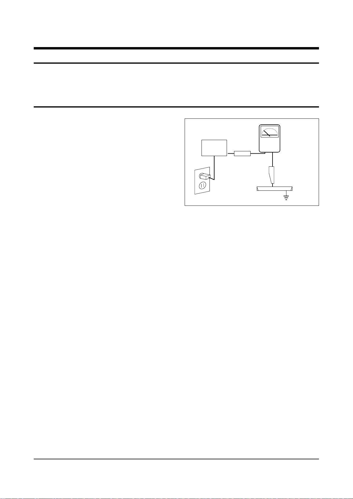
4. Leakage Current Hot Check (Figure 1-1):
Warning: Do not use an isolation
transformer during this test. Use a leakagecurrent tester or a metering system that
complies with American National Standards
Institute (ANSI C101.1, Leakage Current for
Appliances), and Underwriters Laboratories
(UL Publication UL1950.5.2).
5. With the unit completely reassembled, plug
the AC line cord directly into the power
outlet. With the unit’s AC switch first in the
ON position and then OFF, measure the
current between a known earth ground (metal
water pipe, conduit, etc.) and all exposed
metal parts, including: antennas, handle
brackets, metal cabinets, screwheads and
control shafts. The current measured should
not exceed 3.5 milliamp. Reverse the powerplug prongs in the AC outlet and repeat the
test.
Fig. 1-1 AC Leakage Test
6. Antenna Cold Check:
With the unit’s AC plug disconnected from the
AC source, connect an electrical jumper across
the two AC prongs. Connect one lead of the
ohmmeter to an AC prong. Connect the other
lead to the coaxial connector.
7. High Voltage Limits:
High voltage must be measured each time servicing is done on the B+, horizontal deflection
or high voltage circuits.
Precautions
Samsung Electronics 1-1
LEAKAGE
CURRENT
TESTER
DEVICE
UNDER
TEST
TEST ALL
EXPOSED METAL
SURFACES
2-WIRE CORD
ALSO TEST WITH
PLUG REVERSED
(USING AC ADAPTER
PLUG AS REQUIRED)
EARTH
GROUND
(READING SHOULD
NOT BE ABOVE
0.5mA)
Follow these safety, servicing and ESD precautions to prevent damage and protect against potential
hazards such as electrical shock and X-rays.

1-2 Safety Precautions (Continued)
8. High voltage is maintained within specified
limits by close-tolerance, safety-related
components and adjustments. If the high
voltage exceeds the specified limits, check
each of the special components.
9. Design Alteration Warning:
Never alter or add to the mechanical or
electrical design of this unit. Example: Do not
add auxiliary audio or video connectors. Such
alterations might create a safety hazard. Also,
any design changes or additions will void the
manufacturer’s warranty.
10. Hot Chassis Warning:
Some TV receiver chassis are electrically
connected directly to one conductor of the AC
power cord. If an isolation transformer is not
used, these units may be safely serviced only
if the AC power plug is inserted so that the
chassis is connected to the ground side of the
AC source.
To confirm that the AC power plug is inserted
correctly, do the following: Using an AC
voltmeter, measure the voltage between the
chassis and a known earth ground. If the
reading is greater than 1.0V, remove the AC
power plug, reverse its polarity and reinsert.
Re-measure the voltage between the chassis
and ground.
11. Some TV chassis are designed to operate with
85 volts AC between chassis and ground,
regardless of the AC plug polarity. These units
can be safely serviced only if an isolation
transformer inserted between the receiver and
the power source.
12. Some TV chassis have a secondary ground
system in addition to the main chassis ground.
This secondary ground system is not
isolated from the AC power line. The two
ground systems are electrically separated by
insulating material that must not be defeated
or altered.
13. Components, parts and wiring that appear to
have overheated or that are otherwise
damaged should be replaced with parts that
meet the original specifications. Always
determine the cause of damage or overheating, and correct any potential hazards.
14. Observe the original lead dress, especially
near the following areas: Antenna wiring,
sharp edges, and especially the AC and high
voltage power supplies. Always inspect for
pinched, out-of-place, or frayed wiring. Do
not change the spacing between components
and the printed circuit board. Check the AC
power cord for damage. Make sure that leads
and components do not touch thermally hot
parts.
15. Product Safety Notice:
Some electrical and mechanical parts have
special safety-related characteristics which
might not be obvious from visual inspection.
These safety features and the protection they
give might be lost if the replacement component differs from the original—even if the
replacement is rated for higher voltage,
wattage, etc.
Components that are critical for safety are
indicated in the circuit diagram by shading,
( ) or ( ).
Use replacement components that have the
same ratings, especially for flame resistance
and dielectric strength specifications.
A replacement part that does not have the
same safety characteristics as the original
might create shock, fire or other hazards.
Precautions
1-2 Samsung Electronics

1-3 Servicing Precautions
1. Servicing precautions are printed on the
cabinet. Follow them.
2. Always unplug the unit’s AC power cord from
the AC power source before attempting to: (a)
Remove or reinstall any component or
assembly, (b) Disconnect an electrical plug or
connector, (c) Connect a test component in
parallel with an electrolytic capacitor.
3. Some components are raised above the printed
circuit board for safety. An insulation tube or
tape is sometimes used. The internal wiring is
sometimes clamped to prevent contact with
thermally hot components. Reinstall all such
elements to their original position.
4. After servicing, always check that the screws,
components and wiring have been correctly
reinstalled. Make sure that the portion around
the serviced part has not been damaged.
5. Check the insulation between the blades of the
AC plug and accessible conductive parts
(examples: metal panels, input terminals and
earphone jacks).
6. Never defeat any of the B+ voltage interlocks.
Do not apply AC power to the unit (or any of
its assemblies) unless all solid-state heat sinks
are correctly installed.
7. Always connect a test instrument’s ground
lead to the instrument chassis ground before
connecting the positive lead; always remove
the instrument’s ground lead last.
8. Plasma display panels have partial afterimages when a same picture continues to be displayed for a certain time. This happens due to
the degradation of brightness caused by a
scale-down effect.
To prevent such afterimages when displaying
a same picture for a certain time, be sure to
reduce the level of brightness and contrast.
ex) Contrast : 50 or 75, Brightness : 25
9. Plasma display is an array of pixels(cells).
Therefore, if at least 99.9% pixels keep normal,
the appropriate panel is judged as ‘approved
product.’ Even though some of pixels keep
luminescent or always light off, do not worry
because the panel is approved.
Precautions
Samsung Electronics 1-3
Warning 1 : First read the “Safety Precautions” section of this manual. If some unforeseen circumstance creates a
conflict between the servicing and safety precautions, always follow the safety precautions.
Warning 2 : An electrolytic capacitor installed with the wrong polarity might explode.

1-4 Precautions for Electrostatically Sensitive Devices (ESDs)
1. Some semiconductor (“solid state”) devices
are easily damaged by static electricity. Such
components are called Electrostatically
Sensitive Devices (ESDs); examples include
integrated circuits and some field-effect
transistors. The following techniques will
reduce the occurrence of component damage
caused by static electricity.
2. Immediately before handling any semicon
ductor components or assemblies, drain the
electrostatic charge from your body by
touching a known earth ground. Alternatively,
wear a discharging wrist-strap device. (Be
sure to remove it prior to applying power—
this is an electric shock precaution.)
3. After removing an ESD-equipped assembly,
place it on a conductive surface such as
aluminum foil to prevent accumulation of
electrostatic charge.
4. Do not use freon-propelled chemicals. These
can generate electrical charges that damage
ESDs.
5. Use only a grounded-tip soldering iron when
soldering or unsoldering ESDs.
6. Use only an anti-static solder removal device.
Many solder removal devices are not rated as
“anti-static”; these can accumulate sufficient
electrical charge to damage ESDs.
7. Do not remove a replacement ESD from its
protective package until you are ready to
install it. Most replacement ESDs are
packaged with leads that are electrically
shorted together by conductive foam,
aluminum foil or other conductive materials.
8. Immediately before removing the protective
material from the leads of a replacement ESD,
touch the protective material to the chassis or
circuit assembly into which the device will be
installed.
9. Minimize body motions when handling
unpackaged replacement ESDs. Motions such
as brushing clothes together, or lifting a foot
from a carpeted floor can generate enough
static electricity to damage an ESD.
Precautions
1-4 Samsung Electronics
CAUTION
These servicing instructions are for use by
qualified service personnel only.
To reduce the risk of electric shock do not
perform any servicing other than that contained
in the operating instructions unless you are
qualified to do so.

Reference Information
Samsung Electronics 2-1
2. Reference Information
2-1 Tables of Abbreviations and Acronyms
A
Ah
Å
dB
dBm
°C
°F
°K
F
G
GHz
g
H
Hz
h
ips
kWh
kg
kHz
kΩ
km
km/h
kV
kVA
kW
I
MHz
Ampere
Ampere-hour
Angstrom
Decibel
Decibel Referenced to One
Milliwatt
Degree Celsius
Degree Fahrenheit
degree Kelvin
Farad
Gauss
Gigahertz
Gram
Henry
Hertz
Hour
Inches Per Second
Kilowatt-hour
Kilogram
Kilohertz
Kilohm
Kilometer
Kilometer Per Hour
Kilovolt
Kilovolt-ampere
Kilowatt
Liter
Megahertz
MV
MW
MΩ
m
µA
µF
µH
µm
µs
µW
mA
mg
mH
mI
mm
ms
mV
nF
Ω
pF
Ib
rpm
rps
s
V
VA
W
Wh
Megavolt
Megawatt
Megohm
Meter
Microampere
Microfarad
Microhenry
Micrometer
Microsecond
Microwatt
Milliampere
Milligram
Millihenry
Milliliter
Millimeter
Millisecond
Millivolt
Nanofarad
Ohm
Picofarad
Pound
Revolutions Per Minute
Revolutions Per Second
Second (Time)
Volt
Volt-ampere
Watt
Watt-hour
Table 2-1 Abbreviations

Reference Information
2-2 Samsung Electronics
Table 2-2 Table of Acronyms
ABL
AC
ACC
AF
AFC
AFT
AGC
AM
ANSI
APC
APC
A/V
AVC
BAL
BPF
B-Y
CATV
CB
CCD
CCTV
Ch
CRT
CW
DC
DVM
EIA
ESD
ESD
FBP
FBT
FF
FM
FS
GND
G-Y
H
HF
HI-FI
IC
IC
IF
Automatic Brightness Limiter
Alternating Current
Automatic Chroma Control
Audio Frequency
Automatic Frequency Control
Automatic Fine Tuning
Automatic Gain Control
Amplitude Modulation
American National Standards Institute
Automatic Phase Control
Automatic Picture Control
Audio-Video
Automatic Volume Control
Balance
Bandpass Filter
Blue-Y
Community Antenna Television (Cable TV)
Citizens Band
Charge Coupled Device
Closed Circuit Television
Channel
Cathode Ray Tube
Continuous Wave
Direct Current
Digital Volt Meter
Electronics Industries Association
Electrostatic Discharge
Electrostatically Sensitive Device
Feedback Pulse
Flyback Transformer
Flip-Flop
Frequency Modulation
Fail Safe
Ground
Green-Y
High
High-Frequency
High Fidelity
Inductance-Capacitance
Integrated Circuit
Intermediate Frequency
I/O
L
L
LED
LF
MOSFET
MTS
NAB
NEC
NTSC
OSD
PCB
PLL
PWM
QIF
R
RC
RF
R-Y
SAP
SAW
SIF
SMPS
S/N
SW
TP
TTL
TV
UHF
UL
UV
VCD
VCO
VCXO
VHF
VIF
VR
VTR
VTVM
TR
Input/output
Left
Low
Light Emitting Diode
Low Frequency
Metal-Oxide-Semiconductor-Field-Effect-Tr
Multi-channel Television Sound
National Association of Broadcasters
National Electric Code
National Television Systems Committee
On Screen Display
Printed Circuit Board
Phase-Locked Loop
Pulse Width Modulation
Quadrature Intermediate Frequency
Right
Resistor & Capacitor
Radio Frequency
Red-Y
Second Audio Program
Surface Acoustic Wave(Filter)
Sound Intermediate Frequency
Switching Mode Power Supply
Signal/Noise
Switch
Test Point
Transistor Transistor Logic
Television
Ultra High Frequency
Underwriters Laboratories
Ultraviolet
Variable-Capacitance Diode
Voltage Controlled Oscillator
Voltage Controlled Crystal Oscillator
Very High Frequency
Video Intermediate Frequency
Variable Resistor
Video Tape Recorder
Vacuum Tube Voltmeter
Transistor
Specifications
Samsung Electronics 3-1
3. Specifications
MODEL
3-1 Display(PDP Monitor)
Display
Remote Control
Display
Remote Control
Voltage
Power Consumption
Number of Pixels
Screen Size
AUDIO Input
AUDIO Output
VIDEO Input
Dimensions
(mm/inch)
Weight
PPM42S2
1038.8(W) x 89(D) x 635(H)mm / 40.9(W) x 3.5(D) x 25(H) Inches
54(W) x 31.5(D) x 220(H)mm / 2.13(W) x 1.24(D) x 8.66(H) Inches
32Kg / 70.55\bs
150g (Including batteries) / 0.33\bs
AC 100-240V, 50/60Hz
310 Watts
852(H) X 480(V)
106Cm / 42 Inches
VIDEO / S-VIDEO
COMPONENT
PC (RGB)
7W + 7W (8Ω)
VIDEO
S-VIDEO
COMPONENT 1(480i) / 2 (480p/720p/1080i)
PC (RGB 1 : D-SUB / RGB 2 : BNC)

3-2 Samsung Electronics
MENO
Alignment and Adjustments
Samsung Electronics 4-1
4. Alignment and Adjustments
4-1 Service Mode
4-1-1 SERVICE MODE ENTRY METHOD (General Transmitter)
1. Turn off the power to make the SET STAND-BY mode.
2. In order to enter the Service Mode, select MUTE-1-8-2-POWER.
* In case entry into SERVICE MODE is unsuccessful, repeat the procedures above.
4-1-2 Initial DISPLAY State in times of SERVICE MODE Switch overs
4-1-2(A) OSD DISPLAY
4-1-2(B) BUTTONS OPERATIONS WITHIN SERVICE MODE
1. PWS364 9. Pinp Control
2. VPC3230 10.OSD Position
3. SDA9400 11. Test Pattern
4. SDA9280 12. Option Table
5. AD9884 - V ideo 13.Reset
6. AD9884 - DTV/PC
7. CXA2101Q-1
8. CXA2101Q-2
Release Time :
Menu
Joystick UP/DOWN
Joystick (LEFT/RIGHT)
Entire menu display
Cursor move to select items
Enable to increase and decrease the data of the selected items
MENU
Alignment and Adjustments
4-2 Samsung Electronics
4-1-3 Details of Control
4-1-3(A) PW364
No OSD
1
2
3
4
5
6
7
8
9
10
11
12
13
14
15
16
H Position
V Position
Red Gain
Green Gain
Blue Gain
Red Offset
Green Offset
Blue Offset
APL On/Off
High Light
Low Light
Shit Pixel
Test
Pixel Number
Shift Line
Time
93
35
113
113
113
139
139
139
1
113
139
on
0
4
4
4
Default of MODE
VIDEO / S-VHS Component1 Component2 PC
30
34
148
148
148
133
133
133
1
148
133
on
0
4
4
4
-
-
-
-
-
-
-
-
-
-
-
-
-
-
-
-
27
20
125
125
125
129
129
129
1
125
129
on
0
4
4
4
Alignment and Adjustments
Samsung Electronics 4-3
4-1-3(B) VPC3230
1
2
3
4
5
6
7
8
9
10
11
12
13
14
Bright YUV
Cont YUV
IF Comp(IFC)
Chroma band(CBW)
Ena Luma
HPLL Speed
Luma Delay
3230 Bright
3230 Contrast
H LPF Y/C(LPF2)
H LPF Chroma(CBW2)
H Peaking (Filter)
Coaring Off/On
PK
Default of MODE
195
27
2
3
1
1
4
146
45
0
0
1
1
3
195
27
2
3
1
1
4
146
45
0
0
2
1
3
-
-
-
-
-
-
-
-
-
-
-
-
-
-
VIDEO / S-VHS Component1 Component2 PC
DO NOT ENTER
No OSD
4-1-3(C) SDA9400
1
2
3
4
5
6
SNR On
VCSNR On
HCSNR On
DTNR On
TNRCLY
TNRCNC
Default of MODE
-
-
-
-
-
-
1
1
0
1
5
5
-
-
-
-
-
-
VIDEO / S-VHS Component1 Component2 PC
DO NOT ENTER
No OSD
Alignment and Adjustments
4-4 Samsung Electronics
1
2
3
4
5
6
7
8
CTI Thresh
CTI Trawid
Y-Delay
LPF Gain
BPF Gain
HPF Gain
Phacom
Cor
Default of MODE
-
-
-
-
-
-
-
-
0
0
11
7
11
12
2
1
-
-
-
-
-
-
-
-
VIDEO / S-VHS Component1 Component2 PC
DO NOT ENTER
4-1-3(E) AD9884
1
2
3
4
5
6
7
Red Gain
Green Gain(Fix)
Blue Gain
Red Offset
Green Offset(Fix)
Blue Offset
Current
Default of MODE
142
132
143
28
32
21
-
143
132
143
38
32
25
1
-
-
-
-
-
-
-
VIDEO / S-VHS Component1 Component2 PC
4-1-3(D) SDA9280
No OSD
No OSD
145
132
137
34
32
27
-

Alignment and Adjustments
Samsung Electronics 4-5
4-1-3(F) CXA2101Q-1
Default of MODE
VIDEO / S-VHS Component1 Component2 PC
No OSD
1
2
3
4
5
6
7
8
9
10
11
12
13
14
15
16
17
18
Sub Bright
Limit Level
System
D-Color
R Drive
G Drive
B Drive
R Cutoff
G Cutoff
B Cutoff
ABL Mode
ABL TH
H sep sel
Fix Sync
V Time Con
H Width
HHD Time Con
Picture
52
0
2
1
32
32
32
32
32
32
0
0
0
0
1
1
0
10
52
0
1
1
32
32
32
32
32
32
0
0
0
0
1
1
0
10
-
-
-
-
-
-
-
-
-
-
-
-
-
-
-
-
-
-
DO NOT ENTER
Alignment and Adjustments
4-6 Samsung Electronics
4-1-3(G) CXA2101Q-2
Default of MODE
VIDEO / S-VHS Component1 Component2 PC
No OSD
1
2
3
4
5
6
7
8
9
10
11
12
13
14
15
16
17
18
HS Mask
Sub Cont
Sub Color
Sub Hue
Sub SHP
R-Y/R
R-Y/B
G-Y/R
G-Y/B
PABL Level
SHP FO
Pre/Over
CTI Level
LTI Level
DC-Tran
D-Pic
Color
Brightness
1
7
14
6
2
7
14
6
7
6
2
0
1
0
1
2
26
35
1
8
14
5
2
7
14
12
5
6
2
0
1
0
2
3
26
37
-
-
-
-
-
-
-
-
-
-
-
-
-
-
-
-
-
-
DO NOT ENTER
Alignment and Adjustments
Samsung Electronics 4-7
4-1-3(H) PinP Control
1
2
3
4
5
6
7
Pip HPos
Pip VPos
Bright YUV
Cont YUV
Luma Delay
3230 Bright
3230 Contrast
Default of MODE
-
-
-
-
-
-
-
6
13
195
27
0
40
38
6
13
195
27
0
40
38
VIDEO / S-VHS Component1 Component2 PC
No OSD
-
-
-
-
-
-
-
Alignment and Adjustments
4-8 Samsung Electronics
Alignment and Adjustments
4-1-4 White Balance Adjust Method
1. Press MUTE-1-8-2-POWER to enter the factory mode.
2. Enter "5. AD9884 - Video" or " 6. AD9884 - DTV/PC".
3. Adjust LOW coordinates as R,B OFFSET and HIGH coordinates as R,B GAIN.
(GREEN is fixed)
4. Press "Menu" Key in remote control to exit.
5. Enter "1. PW364A".
6. Adjust LOW light as "Low Light".
7. Adjust HIGH light as "High Light".
- W/B Adjustment SPEC(Suwon Factory Toshiba PATTERN)
‹ Condition of Signals
! Video,S-VHS, Component1(DVD) : 10-Gray: (0,1,
@,3,4,5,^,7,8,9,10)-ShibaSoku TG71BX
@ Component 2(DTV) : 9 Gray : (0,1,@,3,4,5,^,7,8,9) - LT446 1080i output
# PC : 16 Gray (0,1,2,#,4,5,6,7,8,(,10....15) - TP36B
W/B x y Y(fL) T(K)
VIDEO
(10 Gray)
D T V
(9 Gray)
P C
(16 Gray)
High (^)
Low (@)
High (^)
Low (@)
High (()
Low (#)
Picture Quality
Assessment
Picture Quality
Assessment
Picture Quality
Assessment
285
285
285
285
285
285
295
295
295
295
295
295
19
0.7
21
0.95
14
0.65
9200
9200
9200
9200
9200
9200
Alignment and Adjustments
Samsung Electronics 4-9
Alignment and Adjustments
4-2 PPM42S2 PC Input Mode
IBM PC/AT
Compatible
640 X 350
640 X 400
720 X 400
640 X 480
848 X 480
852 X 480
800 X 600
1024 X 768
P
P
N
N
N
N
N
N
N
N/P
N
N/P
P
P
P
P
N
N
P
P
Video Signal Dot Line
70.086
85.080
85.080
70.087
85.039
59.940
72.809
75.000
85.008
60.000
60.000
56.250
60.317
72.188
75.000
85.061
60.004
70.069
75.029
84.997
31.469
37.861
37.861
31.469
37.927
31.469
37.861
37.500
43.269
29.800
31.731
35.156
37.879
48.077
46.875
53.674
48.363
56.476
60.023
68.677
N
N
P
P
P
N
N
N
N
N/P
N
N/P
P
P
P
P
N
N
P
P
Vertical
Frequency (Hz)
Horizontal
Frequency (KHz)
Vertical
Polarity
Horizontal
Polarity
Alignment and Adjustments
4-10 Samsung Electronics
Alignment and Adjustments
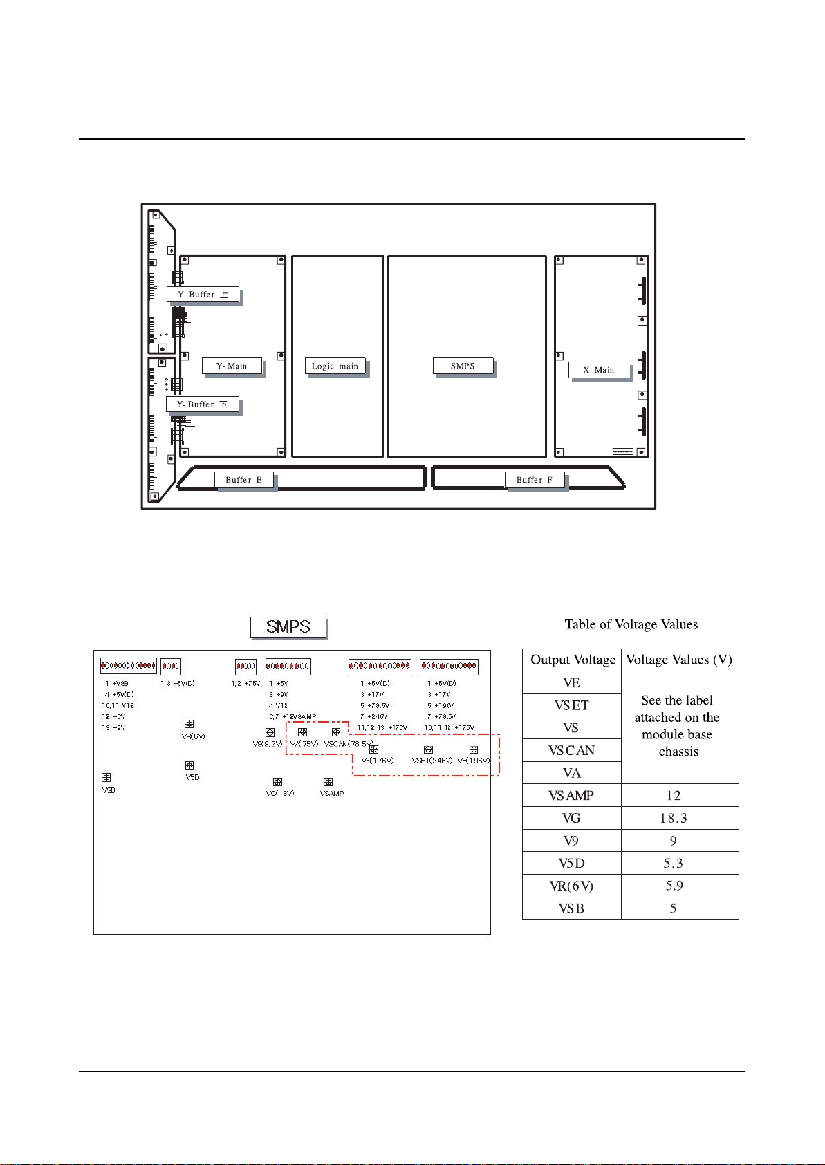
4-3 Discharge Voltage Adjustments When Replacing Main Assay
PDP Driving related Board Layou
Voltage Adjustments
n Adjust all of variable resistances except V9, VG clockwise to decrease the voltage.
nn
For PPM42S2 models, readjust VR (6V) to 5.9V (±0.2V).
n When replacing the X, Y driving boards, avoid waveform adjustments using variable resistance as they
have been adjusted according to the characteristics of PDP panel.
Samsung Electronics 4-11
Alignment and Adjustments
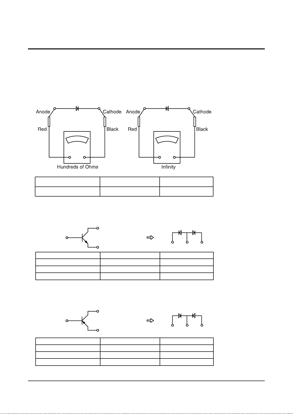
4-4 Fault Finding Using MULTI METER
Parts defects can be found for DIODE TRANSISTOR IC, using MULTI TEST including
Forward/Reverse direction Multi Test. Of course, in case resistance of several ohms and COIL are connected in parallel circuit, the lock out circuit parallel connected to part must be severed.
1.DIODE
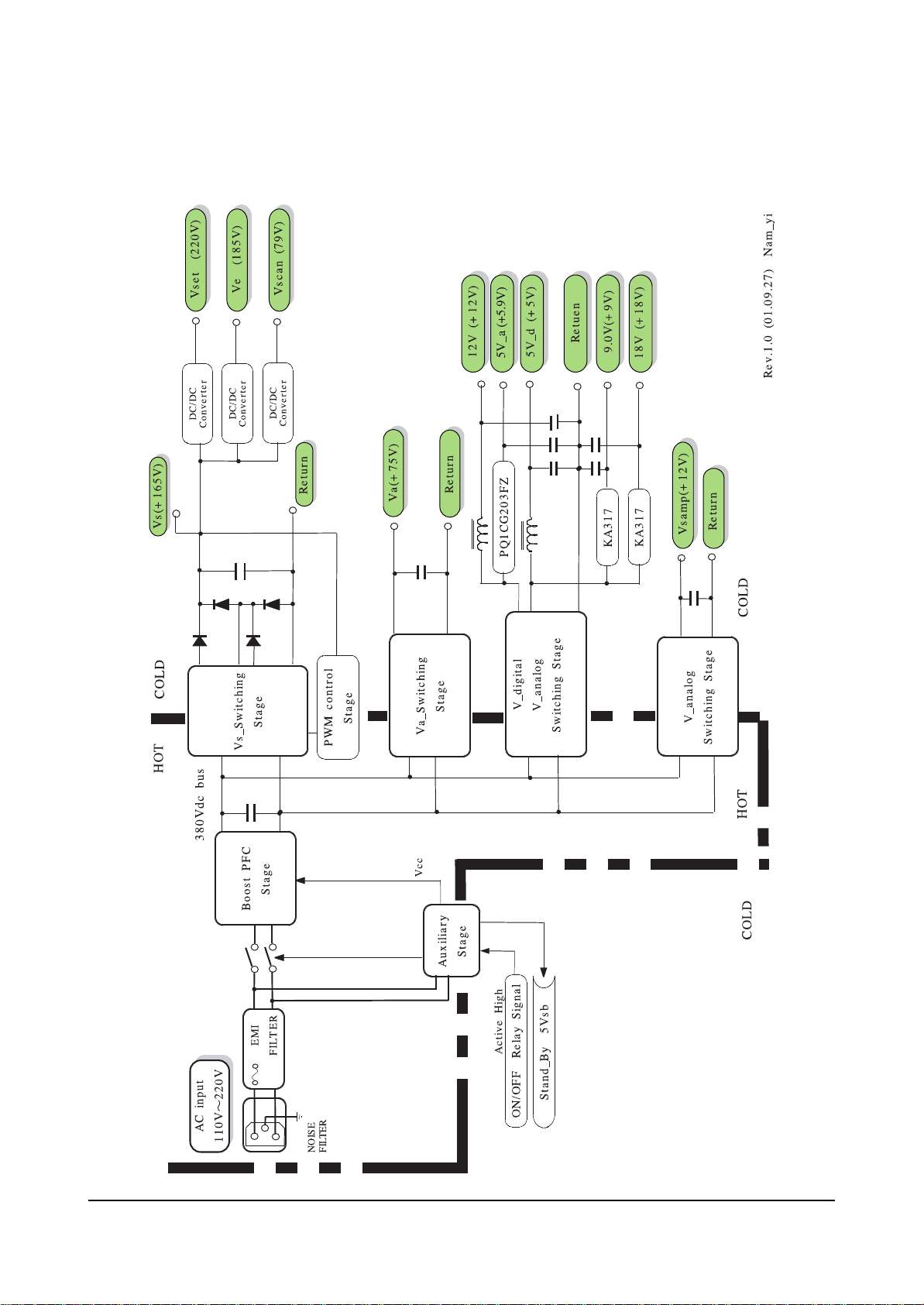
2. TRANSISTOR
l For NPN(KSC815-Y, 2SC2068, 2SC2331-Y)
l For PNP(KSA539-Y)
Forward Direction
Hundreds of ohms
Reverse Direction
Infinity
Between Anode and Cathode
C (COLLECTOR)
E
B(BASE)
BC
C (COLLECTOR)
E
B(BASE)
BC
E (EMITTER)
E (EMITTER)
Forward Direction
Hundreds of ohms
Hundreds of ohms
Infinity
Reverse Direction
Infinity
Infinity
Infinity
Between B and E
Between B and C
Between E and C
Forward Direction
Hundreds of ohms
Hundreds of ohms
Infinity
Reverse Direction
Infinity
Infinity
Infinity
Between B and E
Between B and C
Between E and C
+- +-

4-12 Samsung Electronics
Alignment and Adjustments
3. IC (INTEGRATED CIRCUIT)
IC has built in DIODE against overvoltage in PIN. Generally, except for internal circuit defects, IC defects
can be found, by measuring the DIODE.
› Defects have SHORT(0 ohm) for both forward and reverse direction.
Hundreds of ohms
Forward Direction
Reverse Direction
Varying depending on IC but generally normal
Infinity in DIODE TEST MODE
Circuit Operation Description
Samsung Electronics 5-1
5. Circuit Description
5-1 Power supply
5-1-1 Outline(PDP SMPS)
Considering various related conditions, the switching regulator with good efficiency and allowing for its
small size and lightweight was used as the power supply for PDP. Most of the power supply components
used forward converter, and Vsamp and Vsb used simple flyback converter.
To comply with the international harmonics standards and improve the power factor, active PFC (Power
Factor Correction) was used to rectify AC input into +400V DC output, which in turns used as input to the
switching regulator.
5-1-2 42"SD SMPS SPECIFICATION
5-1-2(A) INPUT
PDP-42PS board is designed so that input power can be used within AC 90 VAC to 264 VAC with
50/60Hz ± 3Hz.
5-1-2(B) OUTPUT
PDP-42PS board provides 13 output switching power supplies (+165Vs, +220Set, +185Ve, +75Va,
+80Scan, +18Vg, +5Vsb, +5V(D), +5.9V(A), +12V. +9V, +12Vfan, and +12Vsamp). The output voltage,
and current requirements for continuous operation are stated below (Table 3).
Table1. Specifications of Output Power Supplies for PDP SMPS
Output Name
Vs
Va
Vscan
Vset
Ve
Vg
Vfan
V9
V5(A)
V5(D)
Vsb
V12
Vsamp
Output Voltage
+165V
+75V
+80V
+220V
+185V
+18.3V
+12V
+9V
+5.9V
+5.3V
+5V
+12V
+12V
Output Current
1.4A
0.5A
0.05A
0.05A
0.05A
0.3A
0.8A
0.3A
1.0A
3.5A
0.4
1.2A
1.5A
Using in PDP driving
Sustain Voltage of Drive Board
Address Voltage of Drive Board
Analog IC Drive Voltage of Video Board
IC Drive Voltage of Logic Board
Stand-by for Remote Control

Circuit Operation Description
5-2 Samsung Electronics
Table 2. Specifications to Protect PDP SMPS
Division
Vs
Va
+5V
OCP Current
5A
2A
10A
OVP Voltage
195V
90V
6.2V
Short Circuit
O.K
O.K
O.K
5-1-2(C) FUNCTION OF BOARD
(1) Remote control
Using 250V/ 10A relay, the board makes remote control available.
(2) Free voltage
The board designed so that input voltage can be used within 90 VAC to 264VAC.
(3) Embedded thermal sensor
The board is equipped with thermal sensor to detect the internal temperature of the unit, and to short
relay when the internal temperature is higher than specified temperature so as to shutdown the unit.
(4) Improvement of power factor
The board is designed using PFC circuit so that PF (Power Factor) can be over 0.95, because low PF
can be a problem in high voltage power.
(5) Protection
The OCP (Over Current Protection), the OVP (Over voltage Protection), and the Short Circuit
Protection functions are added against system malfunction.
Circuit Operation Description
Samsung Electronics 5-3
5-1-2(D) PDP-PS-42 BLOCK DIAGRAM

Circuit Operation Description
5-4 Samsung Electronics
(1) AC-DC Converter
PDP-42PS outputs +400V DC from the common AC power supply using the active PFC booster converter. This converter is designed for improving the power factor and preventing the noise with high
frequency and finally becomes the input power system for the switching regulator on the output side.
(2) Auxiliary Power Supply
The auxiliary power supply is a block generating power of •Ï-com for remote controlling. Once the
power plug is inserted, this block always comes into operation, causing •Ï-com to get into the standby state for the output. Thus, this output is called the stand-by voltage. And with the relay ON signal
inputted through the remote controller, this block turns the mechanical switch of relay to ON for driving the main power supply.
(3) Implementation of Sustain Voltage
As the main part of a SMPS for PDP, sustain voltage must supply a high power, +165V/ 1.4A. It is
designed using forward converter basically. At the output stage two 90V converters are connected
serially for high efficiency and reduction of system size against a single 180V converter.
(4) Implementation of Small Power Output (Va, V(D), V(A), Vfan, V9, Vsamp, Ve, Vset, Vscan, V12, and
Vg)Vset, Ve, and Vscan used DC-DC module. V(D), Va, V12, and Vfan used forward converter, and
Vsamp used flyback converter. V(A), V9, and Vg are simply implemented using switching regulator.
5-1-3 Requirements of PDP SMPS
Since SMPS does not operate alone, but it operates with the load of the whole system, it should be designed
carefully considering the load of the system. In addition, it should be designed considering emerging issues
such as EMC, and protection against heat as well as system stability especially.
5-1-3(A) SAFETY AND REMOTE CONTROL CAPABILITY
Stability is one of the most important requirements for SMPS. SMPS should be designed to prevent
abnormal status due to abnormal load variation so as to keep the system stable, and guarantee customer
safety.
The protection circuits of SMPS include over-current protection (OCP), over voltage protection (OVP),
and under voltage lock-out (UVLO), and short circuit protection circuit. Although each circuit can be
implemented by various procedures, the most popular is implementing with comparator that compares
current value with that of standard and determine abnormality of the circuit.
In addition, surge current protection, insulation management, and static electricity protection circuit
should be added, because it uses commercial power source as an input.
PDP SMPS should be designed using auxiliary power and relay to provide remote control capability.
Circuit Operation Description
Samsung Electronics 5-5
5-1-3(B) THE RELATION BETWEEN POWER CONSUMPTION AND POWER CONVERSION Efficiency
The power consumption and the power conversion efficiency of SMPS affect protection against heat and
system operation much.
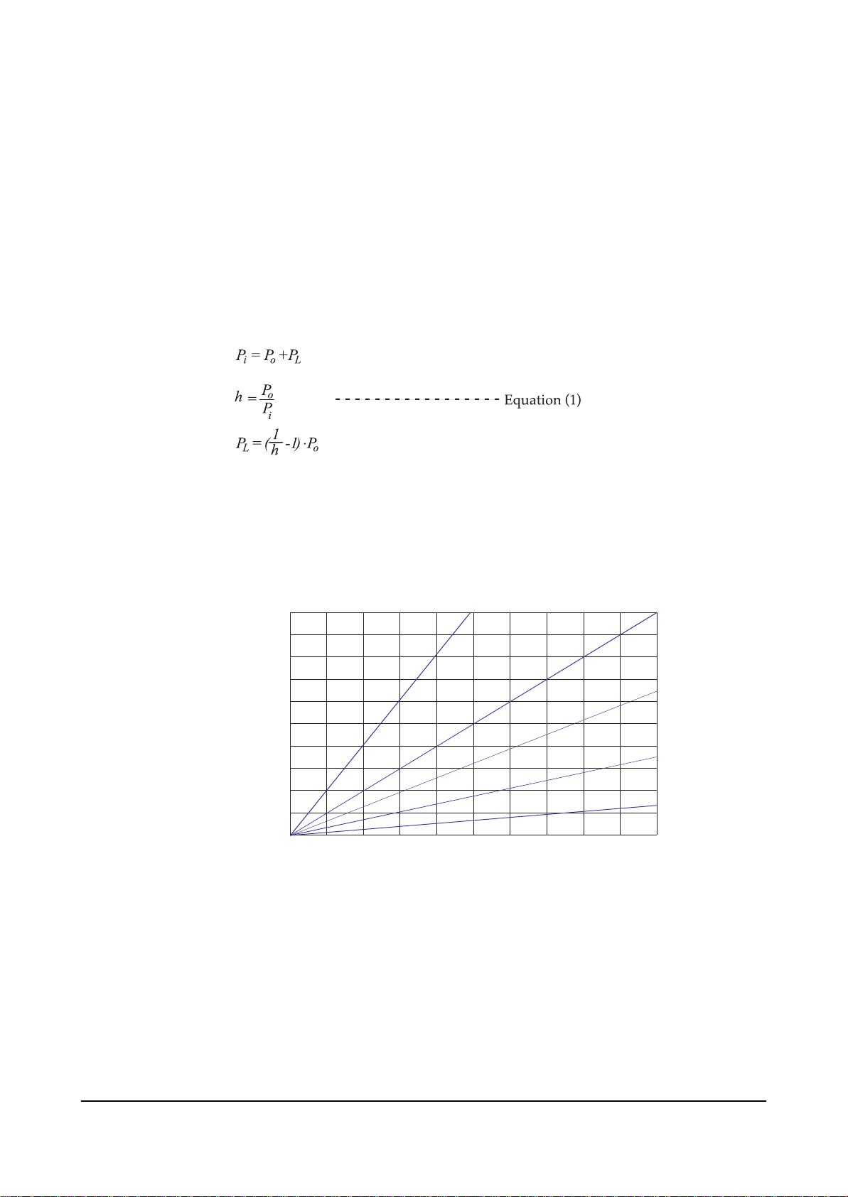
[ If the power conversion efficiency of 100W SMPS is 70%, is the power loss of internal circuit 30W? ]
Output power consumption Po is determined by the multiplication of DC output voltage Vo and output
current Io. Input power consumption Pi is determined by the addition of output power consumption
Po and internal power loss of SMPS Pl.
Provided that the power conversion efficiency is _,
If the power conversion efficiency of 100W SMPS is 70%, the internal power loss is about 42.8W by
Equation (1). If the power conversion efficiency of 400W SMPS for 42"SD is 82%, the internal power loss
is 87.8W by Equation (1). Table 4 shows internal power loss as a function of output power for various
power conversion efficiencies.
Table 4. Power Conversion Efficiency vs. Internal Power Loss
0
20
40
60
80
100
120
140
160
180
200
120 140 160 180 200 240220 260 280 300
50%
60%
90%
70%
80%
η
=
η
=
η
=
η
=
η
=
Internal
Power
Loss ( W)
Direct Current Output Power (W)

Circuit Operation Description
5-6 Samsung Electronics
5-1-3(C) PFC (Power Factor Correction) Circuit Descriptions
The current electric devices use DC power supply and require a rectifier circuit converting AC into DC.
As most rectifier circuits apply a capacitor input type, the rectifier circuit becomes the core of the occurrence of harmonics with lower reverse rate.If various electronic and electric devices are connected to a
power system, high-frequency current will occur due to a power rectifier circuit, a phase control circuit
with power input current of non-sine wave, or components with non-linear load characteristics, such as
capacitor, inductor, etc. As the result, the disturbance of voltage occurs, and finally a power capacitor or
a transformer generates heat, fire or noise occurs, controls malfunction, or the accessed devices abnormally operate or their lives are shortened.To prevent those symptoms, IEC (International
Electrotechnical Commission) regulated standards for Power Supply Harmonics.
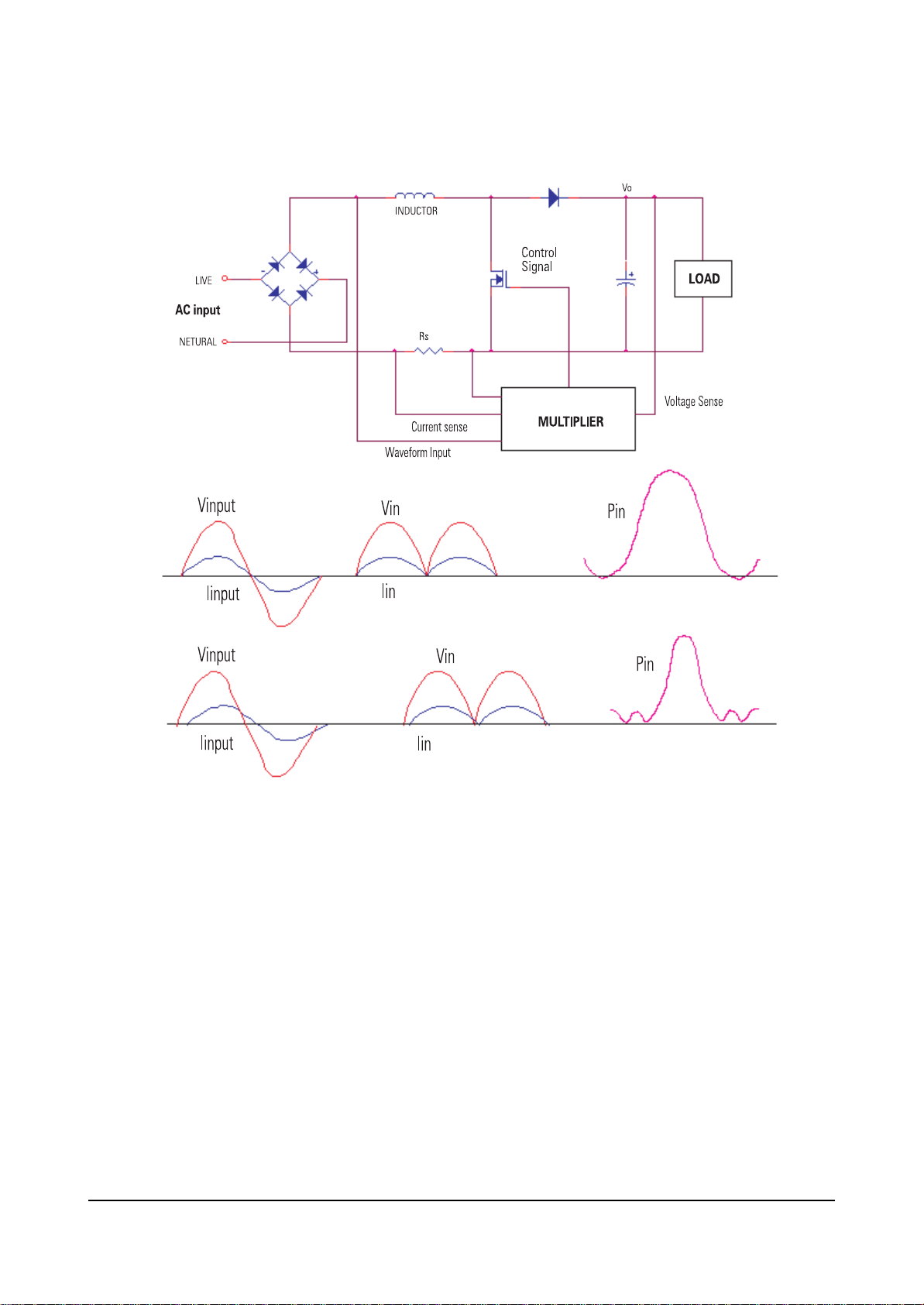
(Refer to IEC 1000-3-2.)Figure 8 shows the basic structure of Active Boost PFC and waveforms.
Standards for Power Supply Harmonics
Scale: Devices accessed to 220V/380V, 230V/400V, 240V/425V and lower than 16A (IEC 100-3-2)
Devices with AC 230V and lower than 16A (IEC 555-2)
Applied Classes :
♦ Class A : Devices not included in another class
♦ Class B : Portable tools
♦ Class C : Lighting devices
♦ Class D : Devices with special current waveforms
Application Schedule : Except the devices less than rating input of 75W (1996~1999)
Except the devices less than rating input of 50W (2000 and after)
Circuit Operation Description
Samsung Electronics 5-7
5-1-3(D) CONCLUSION
Although SMPS (Switching Mode Power Supply) enables small lightweight high-power consumption
power design, it is hard to be used when stability and precise control are required. Power stage for PDP
can be designed using the lightweight SMPS feature. It is important to design SMPS considering
system load, stability, and related international standards.
The architecture and the pulse of active boost PFC

Circuit Operation Description
5-8 Samsung Electronics
5-2 Driver Circuit
5-2-1 Driver Circuit Overview
5-2-1(A) WHAT IS THE DEFINITION OF DRIVE CIRCUIT?
It is a circuit generating an appropriate pulse (High voltage pulse) and then driving the panel to implement
images in the external terminals (X electrode group, Y electrode group and address electrode), and this high
voltage switching pulse is generated by a combination of MOSFET’s.
5-2-1(B) PANEL DRIVING PRINCIPLES
In PDP, images are implemented by impressing voltage on the X electrode, Y electrode and address electrode, components of each pixel on the panel, under appropriate conditions. Currently, ADS (Address &
Display Separate: Driving is made by separating address and sustaining sections) is most widely used to
generate the drive pulse. Discharges conducted within PDP pixels using this method can largely be classified into 3 types, as follows:
(1) Address discharge : This functions to generate wall voltage within pixels to be lighted by addressing
information to them (i.e., impressing data voltage)
(2) Sustain discharge : This means a display section where only pixels with wall voltage by the address
discharge display self-sustaining discharge by the support of such wall voltage. (Optic outputs realizing images are generated.)
(3) Erase discharge : To have address discharge occur selectively in pixels, all pixels in the panel must
have the same conditions (i.e., the same state of wall and space electric discharges). The ramp reset
discharge section, therefore, is important to secure the drive margin, and methods most widely used
to date include wall voltage controlling by ramp pulse.
 Loading...