

Page 1

PLASMA DISPLAY TV
Chassis : D74D(N_42HD)_Spirra
Model : PL42P7HPX/XAO
PLASMA DISPLAY TV FEATURES
■■
DTV Ready PDP TV
■
Supreme Picture Quality
Supreme Convenience Quality
■■
RF, HDMI, PC (Analog), 2 Component,
Video, S-Video
■
Slim line design
■■
Energy Saving
SERVICE
Manual
PL-42P7HP
Page 2

This Service Manual is a property of Samsung Electronics Co.,Ltd.
Any unauthorized use of Manual can be punished under applicable
International and/or domestic law.
© Samsung Electronics Co., Ltd. Jun. 2006
Printed in Korea
AA82-03799A
Page 3

Table of Contents
Chapter 1 Precaution
■ 1-1 Safety Precautions . . . . . . . . . . . . . . . . . . . . . . . . . . . . . . . . . . . . . . . . . . . . . . . . . . . . . . . . . . . 1-1
■ 1-2 Servicing Precautions . . . . . . . . . . . . . . . . . . . . . . . . . . . . . . . . . . . . . . . . . . . . . . . . . . . . . . . . 1-3
■ 1-3 Static Electricity Precautions . . . . . . . . . . . . . . . . . . . . . . . . . . . . . . . . . . . . . . . . . . . . . . . . . . . 1-4
■ 1-4 Installation Precautions . . . . . . . . . . . . . . . . . . . . . . . . . . . . . . . . . . . . . . . . . . . . . . . . . . . . . . . 1-5
Chapter 2 Product Specification
■ 2-1 Product Features . . . . . . . . . . . . . . . . . . . . . . . . . . . . . . . . . . . . . . . . . . . . . . . . . . . . . . . . . . . . 2-1
■ 2-2 Key Features . . . . . . . . . . . . . . . . . . . . . . . . . . . . . . . . . . . . . . . . . . . . . . . . . . . . . . . . . . . . . . . 2-2
■ 2-3 Specifications Analysis . . . . . . . . . . . . . . . . . . . . . . . . . . . . . . . . . . . . . . . . . . . . . . . . . . . . . . . . 2-5
■ 2-4 Accessories . . . . . . . . . . . . . . . . . . . . . . . . . . . . . . . . . . . . . . . . . . . . . . . . . . . . . . . . . . . . . . . . 2-6
Chapter 3 Alignment & Adjustment
■ 3-1 Service Instruction . . . . . . . . . . . . . . . . . . . . . . . . . . . . . . . . . . . . . . . . . . . . . . . . . . . . . . . . . . . 3-1
■ 3-2 How to Access Service Mode . . . . . . . . . . . . . . . . . . . . . . . . . . . . . . . . . . . . . . . . . . . . . . . . . . . 3-2
■ 3-3 Factory Data . . . . . . . . . . . . . . . . . . . . . . . . . . . . . . . . . . . . . . . . . . . . . . . . . . . . . . . . . . . . . . . . 3-3
■ 3-4 Service Adjustment . . . . . . . . . . . . . . . . . . . . . . . . . . . . . . . . . . . . . . . . . . . . . . . . . . . . . . . . . . 3-11
■ 3-5 Software Upgrade . . . . . . . . . . . . . . . . . . . . . . . . . . . . . . . . . . . . . . . . . . . . . . . . . . . . . . . . . . . 3-14
■ 3-6 Replacements & Calibration . . . . . . . . . . . . . . . . . . . . . . . . . . . . . . . . . . . . . . . . . . . . . . . . . . . . 3-15
Chapter 4 Exploded View & Part List
■ 4-1 PL42P7HPX/XAO . . . . . . . . . . . . . . . . . . . . . . . . . . . . . . . . . . . . . . . . . . . . . . . . . . . . . . . . . . . 4-1
Chapter 5 Electrical Part List
■ 5-1 PL42P7HPX/XAO Service Item . . . . . . . . . . . . . . . . . . . . . . . . . . . . . . . . . . . . . . . . . . . . . . . . . 5-1
Chapter 6 Troubleshooting
■ 6-1 First Checklist for Troubleshooting . . . . . . . . . . . . . . . . . . . . . . . . . . . . . . . . . . . . . . . . . . . . . . . 6-1
■ 6-2 Checkpoints by Error Mode . . . . . . . . . . . . . . . . . . . . . . . . . . . . . . . . . . . . . . . . . . . . . . . . . . . . 6-2
■ 6-3 Troubleshooting Procedures by ASS'Y . . . . . . . . . . . . . . . . . . . . . . . . . . . . . . . . . . . . . . . . . . . 6-13
Chapter 7 Block Diagram
■ 7-1 Overall Block Diagram . . . . . . . . . . . . . . . . . . . . . . . . . . . . . . . . . . . . . . . . . . . . . . . . . . . . . . . . 7-1
■ 7-2 Partial Block Diagram . . . . . . . . . . . . . . . . . . . . . . . . . . . . . . . . . . . . . . . . . . . . . . . . . . . . . . . . . 7-3
Chapter 8 Wiring Diagram
■ 8-1 Overall Wiring . . . . . . . . . . . . . . . . . . . . . . . . . . . . . . . . . . . . . . . . . . . . . . . . . . . . . . . . . . . . . . . 8-1
■ 8-2 Partial Wiring . . . . . . . . . . . . . . . . . . . . . . . . . . . . . . . . . . . . . . . . . . . . . . . . . . . . . . . . . . . . . . . 8-3
Page 4

Chapter 9 PCB Diagram
■ 9-1 Main Board . . . . . . . . . . . . . . . . . . . . . . . . . . . . . . . . . . . . . . . . . . . . . . . . . . . . . . . . . . . . . . . . . 9-1
■ 9-2 Power & IR Board . . . . . . . . . . . . . . . . . . . . . . . . . . . . . . . . . . . . . . . . . . . . . . . . . . . . . . . . . . . . 9-4
■ 9-3 Function Board . . . . . . . . . . . . . . . . . . . . . . . . . . . . . . . . . . . . . . . . . . . . . . . . . . . . . . . . . . . . . . 9-4
■ 9-4 Side AV Board . . . . . . . . . . . . . . . . . . . . . . . . . . . . . . . . . . . . . . . . . . . . . . . . . . . . . . . . . . . . . . 9-4
■ 9-5 Main SMPS Board . . . . . . . . . . . . . . . . . . . . . . . . . . . . . . . . . . . . . . . . . . . . . . . . . . . . . . . . . . . 9-5
■ 9-6 DC-DC SMPS Board . . . . . . . . . . . . . . . . . . . . . . . . . . . . . . . . . . . . . . . . . . . . . . . . . . . . . . . . . 9-6
■ 9-7 PDP Module . . . . . . . . . . . . . . . . . . . . . . . . . . . . . . . . . . . . . . . . . . . . . . . . . . . . . . . . . . . . . . . . 9-7
Chapter 10 Schematic Diagram
■ 10-1 Analog . . . . . . . . . . . . . . . . . . . . . . . . . . . . . . . . . . . . . . . . . . . . . . . . . . . . . . . . . . . . . . . . . . . 10-1
Chapter 11 Operation Instruction & Installation
■ 11-1 Product Features and Functions . . . . . . . . . . . . . . . . . . . . . . . . . . . . . . . . . . . . . . . . . . . . . . . 11-1
■ 11-2 Installation Notes and Precautions . . . . . . . . . . . . . . . . . . . . . . . . . . . . . . . . . . . . . . . . . . . . . . 11-5
Chapter 12 Disassembly & Reassembly
■ 12-1 Overhaul Disassembly & Reassembly . . . . . . . . . . . . . . . . . . . . . . . . . . . . . . . . . . . . . . . . . . . 12-1
Chapter 13 Circuit Description
■ 13-1 Power ON/OFF Signal Timing Sequence . . . . . . . . . . . . . . . . . . . . . . . . . . . . . . . . . . . . . . . . . 13-1
■ 13-2 Partial Block Description . . . . . . . . . . . . . . . . . . . . . . . . . . . . . . . . . . . . . . . . . . . . . . . . . . . . . 13-2
Chapter 14 Reference Information
■ 14-1 Other issues related to other products . . . . . . . . . . . . . . . . . . . . . . . . . . . . . . . . . . . . . . . . . . . 14-1
■ 14-2 Technical Terms . . . . . . . . . . . . . . . . . . . . . . . . . . . . . . . . . . . . . . . . . . . . . . . . . . . . . . . . . . . . 14-3
Page 5
1. Make sure all protective devices are properly installed
including non-metallic handles and compartment covers
when installing or re-installing the chassis or chassis
assemblies.
2. Make sure that no gaps exist between the cabinets for
children to insert their fingers in to prevent children from
receiving electric shocks. Gaps mentioned above include
ventilation holes of a too great magnitude between the
PDP module and the cabinet mask, and the improper
installation of the rear cabinet.
Errors may occur when the resistance is below 1.0 ㏁ or
over 5.2 ㏁.
In these cases, make sure that the device is repaired
before sending it back to the customer.
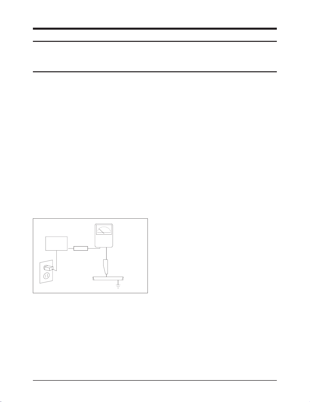
3. Check for Electricity Leakage (Figure 1-1)
Warning: Do not use an insulated transformer for checking the leakage. Use only those current leakage testers
or mirroring systems that comply with ANSIC 101.1 and
the Underwriter Laboratory's specifications (UL1410,
59.7).
Fig. 1-1 AC Leakage Test
4. A high voltage is maintained within the specified limits
using safety parts, calibration and tolerances. When
voltage exceeds the specified limits, check each special
part.
5. Warning for Engineering Changes:
Never make any changes or additions to the circuit
design or the internal part for this product.
Ex: Do not add any audio or video accessory
connectors. This might cause physical damage.
Furthermore, any changes or additions to the original
design/engineering will invalidate the warranty.
6. Warning - Hot Chassis:
Some TV chassis are directly connected to one end of
the AC power cord for electrical reasons.
Without insulated transformers, the product can only be
repaired safely when the chassis is connected to the
earthed end of the AC power source.
To make sure the AC power cord is properly connected,
follow the instructions below. Use the voltmeter to
measure the voltage between the chassis and the
earthed ground. If the measurement is over 1.0V, unplug
the AC power cord and change the polarity before reinserting it. Measure the voltage between the chassis
and the ground again.
7. Some TV chassis are shipped with an additional
secondary grounding system. The secondary system is
adjacent to the AC power line. These two grounding
systems are separated in the circuit using an
unbreakable/unchangeable insulation material.
8. When any parts, material or wiring appear overheated or
damaged, replace them with new regular ones
immediately. When any damage or overheating is
detected, correct this immediately and make a regular
check of possible errors.
9. Check for the original shape of the lead, especially that
of the antenna wiring, any sharp edges, the AC power
and the high voltage power. Carefully check if the wiring
is too tight, incorrectly placed or loose. Never change the
space between the part and the printed circuit board.
Check the AC power cord for possible damages. Keep
the part or the lead away from any heat-emitting
materials.
Precaution
Samsung Electronics 1-1
To avoid possible damages or electric shocks or exposure to radiation, follow the instructions below with regard to safety,
installation, service and ESD.
1. Precaution
1-1 Safety Precautions
(READING SHOULD
DEVICE
UNDER
TEST
EXPOSED METAL
2-WIRE CORD
ALSO TEST WITH
PLUG REVERSED
(USING AC ADAPTER
PLUG AS REQUIRED)
TEST ALL
SURFACES
LEAKAGE
CURRENT
TESTER
NOT BE ABOVE
0.5mA)
EARTH
GROUND
Page 6

10. Safety Indication:
Some electrical circuits or device related materials
require special attention to their safety features, which
cannot be viewed by the naked eye. If an original part is
replaced with another irregular one, the safety or
protective features will be lost even if the new one has a
higher voltage or more watts.
Critical safety parts should be bracketed with ( ).
Use only regular parts for replacements (in particular,
flame resistance and dielectric strength specifications).
Irregular parts or materials may cause electric shock or
fire.
Precaution
1-2 Samsung Electronics
!
Page 7

1. The service instructions are printed on the cabinet, and
should be followed by any service personnel.
2. Make sure to unplug the AC power cord from the power
source before starting any repairs.
(a) Remove or re-install parts or assemblies.
(b) Disconnect the electric plug or connector, if any.
(c) Connect the test part in parallel with the electrolytic
capacitor.
3. Some parts are placed at a higher position than the
printed board. Insulated tubes or tapes are used for this
purpose. The internal wiring is clamped using buckles to
avoid contact with heat emitting parts. These parts are
installed back to their original position.
4. After the repair, make sure to check if the screws, parts
or cables are properly installed. Make sure no damage is
caused to the repaired part and its surroundings.
5. Check for insulation between the blade of the AC plug
and that of any conductive materials (i.e. the metal
panel, input terminal, earphone jack, etc).
6. Insulation Check Process: Unplug the power cord from
the AC source and turn the switch on. Connect the insulating resistance meter (500v) to the AC plug blade.
The insulating resistance between the blade of the AC
plug and that of the conductive material should be more
than 1 ㏁.
7. Any B+ interlock should not be damaged.
If the metal heat sink is not properly installed, no
connection to the AC power should be made.
8. Make sure the grounding lead of the tester is connected
to the chassis ground before connecting to the positive
lead. The ground lead of the tester should be removed
last.
9. Beware of risks of any current leakage coming into
contact with the high-capacity capacitor.
10. The sharp edges of the metal material may cause
physical damage, so ensure wearing protective gloves
during the repair.
11. Due to the nature of plasma display panels, partial afterimages may appear if a still picture is displayed on the
screen for a long period of time.
This is caused by brightness deterioration due to the
storage effect of the panel, and to prevent this from
happening, we recommend that the brightness and contrast are reduced.
(e.g.) Contrast: 25, Brightness: 50
Precaution
Samsung Electronics 1-3
Warning 1: First carefully read the "Safety Instruction" in this service manual.
When there is a conflict between the service and the safety instructions, follow the safety instruction at all times.
Warning 2: Any electrolytic capacitor with the wrong polarity will explode.
1-2 Servicing Precautions
Page 8

1-3 Static Electricity Precautions
1. Some semi-conductive ("solid state") devices are
vulnerable to static electricity. These devices are known
as ESD. ESD includes the integrated circuit and the field
effect transistor. To avoid any materials damage from
electrostatic shock, follow the instructions described
below.
2. Remove any static electricity from your body by
connecting the earth ground before handling any
semi-conductive parts or ass'ys. Alternatively, wear a
dischargeable wrist-belt.
(Make sure to remove any static electricity before
connecting the power source - this is a safety instruction
for avoiding electric shock)
3. Remove the ESD ass'y and place it on a conductive
surface such as aluminum foil to prevent accumulating
static electricity.
4. Do not use any Freon-based chemicals.
Such chemicals will generate static electricity that
causes damage to the ESD.
5. Use only grounded-tip irons for soldering purposes.
6. Use only anti-static solder removal devices.
Most solder removal devices do not support an
anti-static feature. A solder removal device without an
anti-static feature can store enough static electricity to
cause damage to the ESD.
7. Do not remove the ESD from the protective box until the
replacement is ready. Most ESD replacements are
covered with lead, which will cause a short to the entire
unit due to the conductive foam, aluminum foil or other
conductive materials.
8. Remove the protective material from the ESD
replacement lead immediately after connecting it to the
chassis or circuit ass'y.
9. Take extreme caution in handling any uncovered ESD
replacements. Actions such as brushing clothes or lifting
your leg from the carpet floor can generate enough static
electricity to damage the ESD.
Precaution
1-4 Samsung Electronics
CAUTION
These servicing instructions are for use by
qualified service personnel only.
To reduce the risk of electric shock do not
perform any servicing other than that contained in the
operating instructions unless you are qualified to do so.
Page 9

Precaution
Samsung Electronics 1-5
1-4 Installation Precautions
1. For safety reasons, more than two people are required
for carrying the product.
2. Keep the power cord away from any heat emitting
devices, as a melted covering may cause fire or electric
shock.
3. Do not place the product in areas with poor ventilation
such as a bookshelf or closet. The increased internal
temperature may cause fire.
4. Bend the external antenna cable when connecting it to
the product. This is a measure to protect it from being
exposed to moisture. Otherwise, it may cause a fire or
electric shock.
5. Make sure to turn the power off and unplug the power
cord from the outlet before repositioning the product.
Also check the antenna cable or the external connectors
if they are fully unplugged. Damage to the cord may
cause fire or electric shock.
6. Keep the antenna far away from any high-voltage cables
and install it firmly. Contact with the high-voltage cable or
the antenna falling over may cause fire or electric shock.
7. When connecting the RF antenna, check for a DTV
receiving system and install a separate DTV reception
antenna for areas with no DTV signal.
8. When installing the product, leave enough space (4")
between the product and the wall for ventilation
purposes.
A rise in temperature within the product may cause fire.
9. When moving a PDP with removable speakers, detach
the speakers first before moving the main body.
Moving the PDP main body without separating the
speakers may cause the speakers to detach, possibly
causing damage or injury.
Page 10

1-6 Samsung Electronics
MEMO
Page 11

Product Specification
Samsung Electronics 2-1
2. Product Specification
2-1 Product Features
■ Chip Description
- SVP-PX (IC611) : SVP-PX contains dual-purposed triple 10-bit high-precision and high speed video ADCs for both PC and
video inputs, the high speed HDMI could support all HDMI inputs up to 135MHz with HDCP format, the highperformance multi-format 3D digital comb video decoder that supports NTSC, PAL, and SECAM*, a HDTV
sync separator, motion adaptive de-interlacing engine, and the video format conversion engine, supporting
multi-window display in many different output modes.
- STV8258DSX (IC503) : Digital Audio Decoder/Processor
- STA323W (IC505) : Audio power amplifiers
Block Specfication Major IC Remark
RF Tuner TCPN3081PA32S(H) SEMCO
Power Input Voltage : AC 100~240V, 50/60Hz
Video
Scaler
SVP-PX TRIDENT
Video Decoder
Sound
Sound Processor STV8258DSX ST Microelectronics
Sound AMP STA323W ST Microelectronics
Audio S/W MM74HC4052
PDP Module Samsung SDI V5.1 42"HD SAMSUNG SDI
Remocon TM87B
Cabinet P7
Page 12
Product Specification
2-2 Samsung Electronics
2-2 Key Features
Model PL-42P7HP
Screen Size 107 Cm / 42 Inches (16:9)
Dimensions (WxDxH) 1055 x 341 x 775 mm (With stand)
Weight 40.4 Kg (With stand)
Voltage AC 100~240V, 50/60Hz
Colour System PAL-M, PAL-N, NTSC
Sound System BG, DK, I, L
Number of Pixels 1024(H) X 768(V)
ANTENNA input VHF, UHF (75Ωunbalanced)
VIDEO input
AV (Side), S-VIDEO (Side)
2 COMPONENT IN (480i/P, 576i/P, 720P, 1080i)
PC IN (MINI D-SUB 15P)
HDMI/DVI IN
AUDIO input
AV (Side), S-VIDEO (Side)
2 Component
PC
DVI
Audio Output
AUDIO OUT
Headphone (Side)
Speaker Output 15W + 15W ( 8Ω)
Page 13

Product Specification
Samsung Electronics 2-3
■ H/W Configuration
- Video : SVP-PX
- Sound : STV8258DSX, STA323W
- Tuner : TCPN3081PA32S(H)
■ S/W Configuration
- Main Micom : M30840SGP (IC202)
- Sub Micom : 3F866BXZZ (IC207)
■ Picture
- System : Video → PAL-M, PAL-N, NTSC
Sound → Analog
- Progressive
- Output resolution : 1024*768
- OSD : Smart user Interface
- Picture Enhancement : FBE
- Still picture, Noise reduction
- Comb Filter : 3D comb filter
- PIP : Large
- Panorama : Wide
■ Sound
- System : Stereo
- Output : 15W + 15W
- Speaker : built-in
■ Feature
- Component Interface (480i/480p/720p/1080i (60Hz), 576i/576p/720p/1080i (50Hz), Y/Pb/Pr)
- Digital Interface : HDMI
- Picture Size : 16:9/Wide 4:3/Zoom/4:3
- Auto Store
- Sleep Timer : 180 minute
- Clock
- Zoom, Previous channel, Blue Screen, Color Tone, Screen Burn Protection
■ Remocon
- TM87B
■ Power Supply
- AC 100~240V, 50/60Hz
■ Power Consumption
- Max Power : 360 W
Page 14

Product Specification
2-4 Samsung Electronics
■ Both screen position and size will vary depending on the type of PC monitor and its resolution.
The table below shows all of the display modes that are supported. (N : Negative, P : Positive)
Video Signal
Resolution
(Dot X Line)
Vertical frequency
(Hz)
Horizontal frequency
(kHz)
Vertical
polarity
Horizontal
polarity
IBM PC / AT
Compatible
640 X 350 70.086 31.469 P N
720 X 400 70.087 31.469 N P
640 X 480
59.940 31.469 N N
70.000 35.000 N/P N/P
72.809 37.861 N N
75.000 37.500 N N
800 X 600
56.250 35.156 N/P N/P
60.317 37.879 P P
70.000 43.750 N/P N/P
72.188 48.077 P P
75.000 46.875 P P
848 X 480
60.000 31.020 P P
74.769 37.684 P N
1024 X 768
60.004 48.363 N N
70.069 56.476 N N
72.000 57.672 N/P N/P
75.029 60.023 P P
▶ The interlace mode is not supported.
▶ The television might operate abnormally if a non-standard video format is selected.
▶ 480i/p, 576i/p, 720p, or 1080i is not available in pc mode.
▶ The PC text quality is optimum in XGA mode (1024 x 768@60Hz).
Page 15

Product Specification
Samsung Electronics 2-5
2-3 Specifications Analysis
Model PS-42Q7H (Audi-42HD) PL-42P7HP (Spirra-42HD)
Design
Basic
Display Type PDP TV PDP TV
Built-In Tuner O O
Resolution 1024 x 768 1024 x 768
PDP Module V5.1 V5.1
Screen Size 42 inches 42 inches
Aspect Ratio 16 : 9 16 : 9
Power Consumption 360 W 360 W
Dimensions (WxDxH) 1055 x 340 x 756.5 mm 1055 x 341 x 775 mm
Weight 39.5 Kg 40.4 Kg
Picture
Brightness 1,100 Cd/m2 1,100 Cd/m2
Contrast Ratio 5000:1 10000:1
Image Enhacer FBE FBE
Audio
Equalizer O O
Auto Volume O O
Surround Sound SRS TruSurround SRS TruSurround
Speaker Output 10 W + 10 W 15 W + 15 W
Speaker Included Included
Features
PIP O O
Double Screen X X
TTX O X
Still Image O O
My Color Control X X
Color Weakness X X
Energy Saving O O
Screen Burn Protection O O
Connections
Antenna 1 Input 1 Input
CVBS 1 AV 1 AV
S-Video 1 Input 1 Input
Component(Y/PB/PR) 2 Input 2 Input
PC(D-SUB) 1 Input 1 Input
DVI X X
HDMI 1 Input 1 Input
Sub Woofer X X
Optical X X
Coaxial X X
Page 16

Product Specification
2-6 Samsung Electronics
2-4 Accessories
Accessories Item Item code Remark
Supplied Accessories
Remote Control /
AAA Batteries
BN59-00557A /
4301-000103
Samsung Service center
Power Cord 3903-000144
Owner's Instructions BN68-00866W
Warranty Card /
Safety Guide Manual
AA68-03727A /
AA68-03242F
Cloth-Clean BN63-01798A
Accessories that can be purchased
additionally
S-VIDEO Cable -
Internal shopping mall
HDMI Cable -
HDMI/DVI cable -
Component Cables (RCA) -
PC Cable -
PC Audio Cable -
Antenna Cable -
Page 17

Alignment & Adjustment
Samsung Electronics 3-1
3. Alignment & Adjustment
3-1 Service Instruction
■ Before Performing After Sales Services
1. Check if the measurement and test equipment is working properly.
2. Secure sufficient work space for disassembling the product.
3. Prepare a soft pad for disassembling the product.
Page 18

Alignment & Adjustment
3-2 Samsung Electronics
3-2 How to Access Service Mode
1. General Remote
To Enter : Power Off → MUTE → 1 → 8 → 2 → Power On
(Interval between key strokes : less than 3 sec)
To Exit : Power Off → On
2. Factory Remote
To Enter : Power On → INFO → FACTORY Key (Interval between key strokes : less than 3 sec)
To Exit : Power Off → On
Press the Factory key twice with a key stroke interval of more than 1 second (Pressing once enters Aging Mode)
3. Settings when entering Factory mode
- Sharp Screen (Dynamic), Color Tone (Cool1), Factory (Dynamic CE Off)
4. Adjustment Procedures
- Channel ▲▼Key : Select an item.
- Volume ◀▶ Key : Adjust the value up or down.
- MENU Key : Save the changes to the EEPROM and return to the higher-level mode.
- Using the Numeric (0~9) keys, you can select a channel.
- Using the SOURCE key, you can switch AV modes.
5. Initial SERVICE MODE DISPLAY State
※ The version of the firmware displayed at the bottom of the screen may differ and the firmware is subject to change for the
improvement of product functions.
※ If you have adjusted the settings in Service Mode, you have to reset the product.
1. Calibration XXXXX XXXXX 7. YC Delay
2. Option Table XXXXX XXXXX 8. Adjust
3. White Balance 9. -----
4. SVP-FX 10. W/B Movie
5. Option Block 11. Checksum
6. STV8258/STA323W 12. Reset
T-SPRN42NUS-XXXX
T-SPRMNUS-S-XXXX Boot Merge:OK
Month / Day / Year
Hour / Min. / Sec.
Page 19

Alignment & Adjustment
Samsung Electronics 3-3
3-3 Factory Data
★ The underlined are items applied during the service adjustment. None of the others should be adjusted.
1. Calibration
ITEM Data
AV Calibration Sucesses
Comp Calibration Sucesses
PC Calibration Sucesses
HDMI Calibration Sucesses
2. Option Byte
ITEM Condition Range A/V, S-VHS Component PC DVI
inch Option Fixed 42 42 42 42
Gamma Fixed AUO AUO AUO AUO
Panel option Fixed AUO_AMVA AUO_AMVA AUO_AMVA AUO_AMVA
2HDMI Fixed OFF OFF OFF OFF
Brt,Sensor Fixed OFF OFF OFF OFF
EnergySave Fixed ON ON ON ON
LBE/FBE Fixed OFF OFF OFF OFF
FRC(Micronas) Fixed OFF OFF OFF OFF
FRC(Samsung) Fixed OFF OFF OFF OFF
LNA Fixed OFF OFF OFF OFF
Carrier Mute Fixed OFF OFF OFF OFF
Auto FM Fixed ON ON ON ON
High Dev. Fixed OFF OFF OFF OFF
ACR Fixed OFF OFF OFF OFF
Dynamic CE Fixed ON ON ON ON
Dynamic Dimming Fixed ON ON ON ON
Color System Fixed Manual Manual Manual Manual
Auto Power Fixed ON ON ON ON
Magazine LNA Fixed OFF OFF OFF OFF
V-Chip ACR Fixed US US US US
Shop Mode Fixed OFF OFF OFF OFF
Debug Fixed OFF OFF OFF OFF
CH. Table Fixed SAMEX SAMEX SAMEX SAMEX
Dynamic Contrast Fixed OFF OFF OFF OFF
V-Chip Fixed OFF OFF OFF OFF
Page 20
Alignment & Adjustment
3-4 Samsung Electronics
3. White Balance
ITEM Condition Range A/V, S-VHS Component PC DVI
Sub-Briteness Adjusted 0~255 104 104 104 104
R-offset Adjusted 0~255 122 122 122 122
G-offset Fixed 0~255 128 128 128 128
B-offset Adjusted 0~255 129 129 129 129
Sub-Contrast Adjusted 0~255 128 128 128 128
R-Gain Adjusted 0~255 137 137 137 137
G-Gain Fixed 0~255 128 128 128 128
B-Gain Adjusted 0~255 136 136 136 136
Page 21
Alignment & Adjustment
Samsung Electronics 3-5
ITEM Condition Range A/V, S-VHS Component PC DVI
Y-Filter Fixed 00H ~ FFH 80H 80H 80H 80H
ITEM Condition Range A/V, S-VHS Component PC DVI
H2Gain Fixed 00 ~ 1FH 08H 10H 10H 10H
H4Gain Fixed 00 ~ 1FH 08H 10H 04H 10H
V2Gain Fixed 00 ~ 1FH 08H 10H 10H 10H
V4Gain Fixed 00 ~ 1FH 08H 10H 04H 10H
Sr2Gain Fixed 00 ~ 1FH 00H 00H 00H 00H
Sr4Gain Fixed 00 ~ 1FH 00H 00H 00H 00H
Sl2Gain Fixed 00 ~ 1FH 00H 00H 00H 00H
Sl4Gian Fixed 00 ~ 1FH 00H 00H 00H 00H
PeaKTh1 Fixed 00H ~ FFH 04H 04H 00H 04H
PeaKTh2 Fixed 00H ~ FFH 40H 40H 30H 40H
PeaKTh3 Fixed 00H ~ FFH 30H 30H 00H 30H
4. SVP-EX
① ComB Filter
② Sharpness
ITEM Condition Range A/V, S-VHS Component PC DVI
YNROFF Fixed 00H ~ FFH 80H 80H 80H 80H
CNROFF Fixed 00H ~ FFH 80H 80H 80H 80H
YNRON Fixed 00H ~ FFH 80H 80H 80H 80H
CNRON Fixed 00H ~ FFH 80H 80H 80H 80H
③ NR
ITEM Condition Range A/V, S-VHS Component PC DVI
R-Offset Adjusted 00H ~ FFH 5AH 56H 51H 56H
G-Offset Adjusted 00H ~ FFH 5AH 56H 50H 56H
B-Of
fet
Adjusted 00H ~ FFH 5BH 56H 50H 56H
R-Gain Adjusted 00H ~ FFH 7CH 7CH 74H 7AH
G-Gain Adjusted 00H ~ FFH 7CH 7CH 7CH 7AH
B-Gain Adjusted 00H ~ FFH 7CH 7CH 81H 7AH
④ RGB Calibration
Page 22
Alignment & Adjustment
3-6 Samsung Electronics
ITEM Condition Range A/V, S-VHS Component PC DVI
TCD3 Cont. Fixed 00H ~ FFH 7DH 78H 78H 78H
TCD3 Bright. Fixed 00H ~ FFH 20H 20H 20H 20H
TCD3 CR Fixed 00H ~ FFH 80H 80H 80H 80H
TCD3 CB Fixed 00H ~ FFH 80H 80H 80H 80H
TCD3 Delay Fixed 00H ~ FFH 00H 00H 00H 00H
A Y offset Fixed 00H ~ FFH 40H 40H 46H 40H
A PB offset Fixed 00H ~ FFH 80H 80H 46H 80H
A PR offset Fixed 00H ~ FFH 80H 80H 47H 80H
A Y Gain Fixed 00H ~ FFH D6H C0H C0H D6H
A PB Gain Fixed 00H ~ FFH FEH 9AH 80H FEH
A PR Gain Fixed 00H ~ FFH FEH 9AH 80H FEH
Black Level Fixed 00H ~ FFH 00H 00H 00H 00H
SVP Bright. Fixed 00H ~ FFH 00H 00H 00H 00H
⑤ ADC Calibration
ITEM Condition Range low high Delta
AV ADC Fixed 00H ~ FFH 10H E8H 04H
Comp ADC Fixed 00H ~ FFH 10H E8H 04H
PC ADC Fixed 00H ~ FFH 10H E8H 04H
ALL RGB Fixed 00H ~ FFH 04H E8H 10H
⑥ Calibration Target
Page 23
Alignment & Adjustment
Samsung Electronics 3-7
5. Option Block (FRC-Micronas, FRC-Samsung, FBE/LBE)
ITEM Condition Range A/V, S-VHS Component PC DVI
Test Pattern Fixed 00H ~ 19H 00H 00H 00H 00H
B St.Tilt Fixed 00H ~ FFH 65H 60H 40H 70H
B St.Gain Fixed 00H ~ FFH 55H 55H 4BH 60H
B St.Ratio Fixed 00H ~ FFH 30H 30H 27H 30H
Skin En Fixed 00H ~ 01H 01H 01H 00H 01H
Skin Gain Fixed 00H ~ FFH 80H 80H 80H 80H
Skin T X Fixed 00H ~ FFH 63H 63H 6EH 63H
Skin T Y Fixed 00H ~ FFH 60H 60H 5FH 60H
White En Fixed 00H ~ FFH 00H 00H 00H 00H
MCM Gain Fixed 00H ~ FFH 80H 80H 80H 80H
White T X Fixed 00H ~ FFH 4FH 4FH 4FH 4FH
White T Y Fixed 00H ~ FFH 54H 54H 54H 54H
CHY Gain1 Fixed 00H ~ FFH 3EH 3EH 3EH 3EH
CHY Gain2 Fixed 00H ~ FFH 42H 42H 42H 42H
CHC Gain1 Fixed 00H ~ FFH 40H 40H 40H 40H
CHC Gain2 Fixed 00H ~ FFH 40H 40H 40H 40H
CHM Gain1 Fixed 00H ~ FFH 3DH 3DH 3DH 3DH
CHM Gain2 Fixed 00H ~ FFH 45H 45H 45H 45H
ColorGain TY Fixed 00H ~ FFH 00H 00H 00H 00H
ColorGain TC Fixed 00H ~ FFH 00H 00H 00H 00H
ColorGain TM Fixed 00H ~ FFH 00H 00H 00H 00H
ColorGain Fixed 00H ~ FFH 85H 85H 80H 95H
ln Gain Fixed 00H ~ FFH 80H 85H 80H 80H
ln Offset Fixed 00H ~ FFH 00H 00H 00H 00H
6. STV8257STA323W
ITEM Condition Range A/V, S-VHS Component PC DVI
Ch1 Volume Fixed 00H ~ FFH 4AH 4AH 4AH 4AH
Ch2 Volume Fixed 00H ~ FFH 4AH 4AH 4AH 4AH
AGC Gain Fixed 00H ~ FFH 07H 07H 07H 07H
AM-Prescale Fixed 00H ~ 3FH 00H 00H 00H 00H
ZWT TH Fixed 00H ~ 0FH 0AH 0AH 0AH 0AH
AV Delay Fixed 00H ~ FFH 55H 55H 55H 55H
Comp delay Fixed 00H ~ FFH 32H 32H 32H 32H
HDMI Delay Fixed 00H ~ FFH 32H 32H 32H 32H
PC Delay Fixed 00H ~ FFH 32H 32H 32H 32H
L1 Att.Rel Th Fixed 00H ~ FFH CBH CBH CBH CBH
Page 24
Alignment & Adjustment
3-8 Samsung Electronics
7. Y/C Delay
ITEM Condition Range A/V, S-VHS Component PC DVI
PAL B/G Fixed 00H ~ FFH 99H 99H 99H 99H
PAL D/K Fixed 00H ~ FFH 88H 88H 88H 88H
PAL I Fixed 00H ~ FFH 88H 88H 88H 88H
SECAM-B/G Fixed 00H ~ FFH 88H 88H 88H 88H
SECAM-D/K Fixed 00H ~ FFH 77H 77H 77H 77H
SECAM-L/L' Fixed 00H ~ FFH 66H 66H 66H 66H
AV PA L N Fixed 00H ~ FFH A8H A8H A8H A8H
AV PA L M Fixed 00H ~ FFH 77H 77H 77H 77H
AV PA L Fixed 00H ~ FFH A8H A8H A8H A8H
AV SECAM Fixed 00H ~ FFH 88H 88H 88H 88H
AV NT3.58 Fixed 00H ~ FFH 98H 98H 98H 98H
AV NT4.43 Fixed 00H ~ FFH CCH CCH CCH CCH
AV PAL60 Fixed 00H ~ FFH 77H 77H 77H 77H
Page 25
Alignment & Adjustment
Samsung Electronics 3-9
8. Adjust
ITEM Condition Range A/V, S-VHS Component PC DVI
V Mute Time Fixed 0 ~255 10 10 10 10
Melody Vol. Fixed 0 ~ 20 9 9 9 9
AnaDmMax Fixed 0 ~ 255 FEH FEH FEH FEH
TTX Cont. Fixed 0 ~ 100 50 50 50 50
TTX Bright. Fixed 0 ~ 100 50 50 50 50
TTX Color Fixed 0 ~ 100 50 50 50 50
Dynamic Contr Fixed 0 ~ 100 100 100 100 100
DYN Color Fixed 0 ~ 100 50 50 50 50
DYN Sharp. Fixed 0 ~ 100 60 60 60 60
STD Cont. Fixed 0 ~ 100 90 90 90 90
STD Bright. Fixed 0 ~ 100 80 80 80 80
STD Color Fixed 0 ~ 100 70 70 70 70
STD Sharp. Fixed 0 ~ 100 70 70 70 70
MOV Cont. Fixed 0 ~ 100 60 60 60 60
MOV Bright. Fixed 0 ~ 100 50 50 50 50
MOV Color Fixed 0 ~ 100 50 50 50 50
MOV Sharp. Fixed 0 ~ 100 40 40 40 40
ITEM Condition Range A/V, S-VHS Component PC DVI
RFDB-1 Level Fixed 0 ~ 255 2 2 2 2
RFDB-2 Level Fixed 0 ~ 255 5 5 5 5
RFDB-3 Level Fixed 0 ~ 255 9 9 9 9
RFDB-4 Level Fixed 0 ~ 255 24 24 24 24
① LNA PLUS
ITEM Condition Range A/V, S-VHS Component PC DVI
Hotel Mode Fixed ON/OFF OFF OFF OFF OFF
PWR Om CH Fixed 0 ~ 99 1 1 1 1
PWR On Vol. Fixed 0 ~ 100 10 10 10 10
Max Volume Fixed 0 ~ 100 100 100 100 100
L.Key Lock Fixed ON/OFF OFF OFF OFF OFF
PWR On Src Fixed AV/S-VHS/.. PC1 PC1 PC1 PC1
② Hotel Option
Page 26
Alignment & Adjustment
3-10 Samsung Electronics
9. -----
10. W/B Movie
ITEM Condition Range A/V, S-VHS Component PC DVI
WB Movie Fixed ON/OFF OFF OFF OFF OFF
Color Mode Fixed Movie Movie Movie Movie Movie
Color Tone Fixed Warm2/255 Warm2 Warm2 Warm2 Warm2
W1 R Gain Fixed 0 ~ 255 129 129 129 129
W1 B Gain Fixed 0 ~ 255 11 5 115 115 115
W1 R Offset Fixed 0 ~ 255 128 128 128 128
W1 B Offset Fixed 0 ~ 255 130 130 130 130
W2 R Gain Fixed 0 ~ 255 133 133 133 133
W2 B Gain Fixed 0 ~ 255 105 105 105 105
W2 R Offset Fixed 0 ~ 255 128 128 128 128
W2 B Offset Fixed 0 ~ 255 133 133 133 133
MOV Cont. Fixed 0 ~ 255 70 70 70 70
MOV Bright. Fixed 0 ~ 255 50 50 50 50
MOV Color Fixed 0 ~ 255 45 45 45 45
MOV Sharp. Fixed 0 ~ 255 25 25 25 25
11. Checksum OC04
12. Reset
Page 27

Alignment & Adjustment
Samsung Electronics 3-11
3-4 Service Adjustment
3-4-1 White Balance - Calibration
If picture color is wrong, do calibration first.
Execute calibration in Factory Mode
1. Source : VIDEO
2. Setting Mode : PAL Video (MODE : #2)
3. Pattern : Pattern #24 (Chess Pattern)
4. Use Equipment : K-7256 or Equipment of equality level
5. Work order
1) Enter by Factory Mode select "1.CALIBRATION".
2) Select "AV CALIBRATION" again in CALIBRAION MENU.
3) After Completing Calibration, come out "Av success". OSD on the screen (bottom-side) for about 3 seconds.
Source AV : PAL composite, Component : 1280*720/60Hz
PC : 1024*768/60Hz
( Chess Pattern )
Page 28
Alignment & Adjustment
3-12 Samsung Electronics
3-4-2 White Balance - Adjustment
If picture color is wrong, check White Balance condition.
Equipment : CA210, Patten : Toshiba
Adjust W/B in Factory Mode
Sub brightness and R/G/B Offset controls low light region
Sub contrast and R/G/B Gain controls high light region
Source AV : PAL composite, Component : 1280*720/60Hz,
HDMI[DVI] : 1280*720/60Hz
[ Test Pattern : MSPG-945 Series Pattern #16 ]
* Color temperature
1500K +/-500, -6 ~-20 MPCD
* Color coordinate
H/L : 270/280 +/- 2
L/L : 270/280 +/- 3, 2.1 Ft +/-0.05 Ft
( SAMSUNG WHITE BALANCE Adjustment PATTERN with FPD )
3-4-3 Conditions for Measurement
1. On the basis of toshiba ABL pattern : High Light level (57 IRE)
- INPUT SIGNAL GENERATOR : MSPG-925LTH
* Mode No 2 : 744X484@60 Hz
No 6 : 1280X720@60 Hz
No 21 : 1024X768@60 Hz
* Pattern No 36 : 16 Color Pattern
No 16 : Toshiba ABL Pattern
2. Optical measuring device : CA210 (FL)
Please use the MSPG-925 LTH generator for model PL-42P7H.
Page 29
Alignment & Adjustment
Samsung Electronics 3-13
3-4-4 Method of Adjustment
1. Adjust the white balance of AV, Component and DVI Modes.
(AV → Component)
a) Set the input to the mode in which the adjustment will be made (RF → DTV → PC → DVI).
* Input signal - VIDEO Mode : Model #2 (744*484 Mode), Pattern #16
- DTV, DVI Mode : Model #6 (1280*720 Mode), Pattern #16
- HDMI Mode : Model #6 (1280*720 Mode), Pattern #16
b) Enter factory color control, confirm the data.
c) Adjust the low light. (Refer to table 1, 2 in adjustment position by mode)
- Adjust sub - Brightness to set the 'Y' value.
- Adjust red offset ('x') and blue offset ('y') to the color coordinates.
* Do not adjust green offset data.
d) Adjust the high light. (Refer to table 1, 2 in adjustment position by mode)
- Adjust red gain ('x') and blue gain ('y') to the color coordinates.
* Do not adjust the green gain and sub-contrast (Y) data.
( SAMSUNG WHITE BALANCE Adjustment PATTERN with FPD )
( SAMSUNG WHITE BALANCE Adjustment PATTERN with FPD )
Low light
Measurement point
Hight light
Measurement point
Page 30
Alignment & Adjustment
3-14 Samsung Electronics
3-5 Software Upgrade
3-5-1 How to Update Flash ROM
1. Installthe Flash Downloader
Connect Set (Service Jack) and Jig Cable to execute Program Update.
2. Flash Downloader program update
- Before Turning on the set, Click "connect" which is under of OSD Screen.
- Turn on the Set.
Page 31

Alignment & Adjustment
Samsung Electronics 3-15
3-6 Replacements & Calibration
* Check items listed after changing each
Replaced Items Code No. Check Items
ASSY PCB MISC-MAIN BN94-01004B
1) Auto Program
2) White Balance Adjust
ASSY PCB P-SMPS(MAIN) BN96-03052A Vs, Va voltage check and adjust
ASSY PCB P-SMPS(DC DC) BN96-01856A Vscan, Vset, Ve voltage check and adjust
ASSY PDP P-LOGIC BOARD BN96-03355A
Not adjustment
ASSY PDP P-X MAIN BOARD BN96-03350A
ASSY PDP P-Y MAIN BOARD BN96-03351A
ASSY PDP P-Y MAIN SCAN BOARD BN96-03352A
ASSY PDP P-ADDRESS E BUFF BOARD BN96-03353A
ASSY PDP P-ADDRESS F BUFF BOARD BN96-03354A
※ When replacing the SMPS (DC DC) or PDP panel, you have to check the voltage printed on the panel sticker and adjust it.
※ The ASS'Y code can be changed, see "5 Chapter. Electrical Part List."
Page 32

Alignment & Adjustment
3-16 Samsung Electronics
Value Board Adjustment
Vs 200
SMPS-MAIN
Va 65
Vset 195
SMPS-DC/DCVe 120
Vscan -190
3-6-1 Voltage Adjustment
1. After replacing the SMPS or PDP panel, you must adjust the voltage referring to the voltage label printed on the panel.
(If you do not adjust the voltage, an abnormal discharge symptom may appear.)
SMPS-MAIN
Voltage Label
SMPS-DC/DC
2. A point of adjusting SMPS-MAIN voltage.
Vs Adjustment
Vs Test point
Va Adjustment
Va Test point
Page 33

Alignment & Adjustment
Samsung Electronics 3-17
3. A point of adjusting SMPS-DC/DC.
Vset (Middle)
Vscan (Right)
Test Point
Vscan/Vset
Adjustment
Point
VE
Adjustment
Point
Ve Test Point
* Use base chassis of PDP panel as GND point.
Page 34

3-18 Samsung Electronics
MEMO
Page 35

4. Exploded View & Part List
Exploded View & Part List
Samsung Electronics 4-1
You can search for the updated part code through ITSELF web site.
URL:http://itself.sec.samsung.co.kr
4-1 PL42P7HPX/XAO
Loc. No. Code No. Description Specification Q'ty SA/SNA Remark
CIS7 AA61-60003B SPRING ETC-CS -,SUS304,-,-,OD11.2,N7,OD1 1 S.N.A
M0006 BN63-02383A COVER-REAR 42C7,PCM,0.5 1 S.N.A
M0013 BN96-03160A ASSY COVER P-REAR 42C7,P7,PCM T0.5 1 S.A
M0020 BN96-03075E ASSY BOARD P-SIDE AV CADILLAC,SJ06-01-00 1 S.A
M0045 BN96-03156A ASSY STAND P-SET 42P7,ABS HB,SF0507,BK23 1 S.A
M0107 BN61-02315D BRACKET-PCB 42C7,SECC,0.8 1 S.N.A
M0 111 BN63-02376A COVER-STAND 42P7,ABS+PMMA,HB,BK23,H/GLOS 1 S.N.A
M0112 BN63-02374E COVER-FRONT 42Q7/P7H,ABS,HB,ASIA,BK23 1 S.N.A
M0115 BN61-02334A BRACKET-STAND 42P7,SECC,2.0 1 S.N.A
M0145 BN96-02784B ASSY BOARD P-FUNCTION CADILLAC,SJ06-01-0 1 S.A
M0150 BN96-03947A ASSY BRACKET P-FILTER BOTTOM 42Q7/P7,AL, 1 S.N.A
T0003 BN96-03951J ASSY COVER P-FRONT 42Q7(HQ),ABS HB,BK23, 1 S.A
T0023 BN96-03173A ASSY COVER P-KNOB POWER 42P7,ABS 1 S.N.A
T0023 BN64-00459A KNOB POWER 42P7,PC,Violet 1 S.N.A
T0044 BN96-03807A ASSY PDP MODULE P M1,42"HD,W1,1024*768,v 1 S.A
T0054 BN96-03164A ASSY HINGE P 42P7 1 S.N.A
T0056 BN63-02386B COVER-DECORATION 42P7,PC SHEET,T0.5,Blac 1 S.N.A
T0059 BN64-00461A INDICATOR LED 42P7,PMMA 1 S.N.A
T0061 BN64-00462A WINDOW-REMOCON 42P7,ACRYL,5% 1 S.N.A
T0074 BN59-00557A REMOCON SPIRRA,TM87B,SAMSUNG 28P+EEPROM, 1 S.A
T0079 BN94-01004B ASSY PCB MISC-MAIN PL42P7HX/XAZ,D74D,SPI 1 S.A
T0175 BN96-03273A ASSY SPEAKER P 8ohm,P7,15W,2Way,3speaker 1 S.A
T0268 3903-000144 CBF-POWER CORD DT,US,BP3/Y,U(IEC C13-RA) 1 S.A
T0448 BN96-03144E ASSY BRACKET P-TERMINAL 42C7S,ASIA,SECC 1 S.N.A
T0456 BN67-00172A GLASS-FILTER EMI 42" Q7, C7 No B/C,Mesh, 1 S.A
T0603 BN64-00460A KNOB-DECORATION POWER 42P7,ABS,HB,AL 1 S.N.A
T0074
T0003
M0112
T0268
T0456
M0150
T0044
M0107
M0045
T0079
T0448
M0020
M0013
M0006
T0056
T0175
T0023
M0145
T0023
T0061
T0059
T0603
CIS7
M0111
T0054
M0115
Page 36

Electrical Part List
5. Electrical Part List
5-1 PL42P7HPX/XAO Service Item
You can search for the updated part code through ITSELF web site.
URL:http://itself.sec.samsung.co.kr
Loc. No. Code No. Description Specification Q'ty SA/SNA Remark
M0013 BN96-03160A ASSY COVER P-REAR 42C7,P7,PCM T0.5 1 S.A
M0045 BN96-03156A ASSY STAND P-SET 42P7,ABS HB,SF0507,BK23 1 S.A
M2893 BN39-00632B LEAD CONNECTOR PS-42E7HX/XEC,UL1617#22,U 1 S.A
M2893 BN39-00667D LEAD CONNECTOR-LVDS AUDI,UL20276#30,31PI 1 S.A
M2893 BN39-00675A LEAD CONNECTOR PUCCINI,UL1007#26,10PIN,1 1 S.A
M2893 BN39-00676A LEAD CONNECTOR PUCCINI,UL1007#26,12PIN,1 1 S.A
T0003 BN96-03951J ASSY COVER P-FRONT 42Q7(HQ),ABS HB,BK23, 1 S.A
T0044 BN96-03807A ASSY PDP MODULE P M1,42"HD,W1,1024*768,v 1 S.A
T0074 BN59-00557A REMOCON SPIRRA,TM87B,SAMSUNG 28P+EEP- 1 S.A
T0079 BN94-01004B ASSY PCB MISC-MAIN PL42P7HX/XAZ,D74D,SPI 1 S.A
T0159 BN96-01856A ASSY PCB P-SMPS SPD-50P5HD(DC_DC),200Vin 1 S.A
T0159 BN96-03052A ASSY PCB P-SMPS PS42E7H,100~240V,245*370 1 S.A
T0175 BN96-03273A ASSY SPEAKER P 8ohm,P7,15W,2Way,3speaker 1 S.A
T1910 BN96-03350A ASSY PDP MODULE P-X MAIN BOARD 42HD,PL42 1 S.A
T1911 BN96-03351A ASSY PDP MODULE P-Y MAIN BOARD 42HD,PL42 1 S.A
T1914 BN96-03353A ASSY PDP MODULE P-ADDRESS E BU 42HD,PL42 1 S.A
T1915 BN96-03354A ASSY PDP MODULE P-ADDRESS F BU 42HD,PL42 1 S.A
T1917 BN96-03355A ASSY PDP MODULE P-LOGIC MAIN B 42HD,PL42 1 S.A
T9698 BN96-03352A ASSY PDP MODULE P-Y MAIN SCAN 42HD,PL42A 1 S.A
5-1Samsung Electronics
Page 37

MEMO
Samsung Electronics5-2
Page 38

Troubleshooting
Samsung Electronics 6-1
1. Check the various cable connections first.
- Check to see if there is a burnt or damaged cable.
- Check to see if there is a disconnected cable connection or a connection is too loose.
- Check to see if the cables are connected according to the connection diagram.
2. Check the power input to the Main Board.
3. Check the voltage in and out between the SMPS ↔ Main Board, between the SMPS ↔ X, Y Main Board, and between the
Logic Boards.
6. Troubleshooting
6-1 First Checklist for Troubleshooting
Page 39

Troubleshooting
6-2 Samsung Electronics
6-2 Checkpoints by Error Mode
6-2-1 No Power
Symptom
- The LEDs on the front panel do not work when connecting the power cord.
- The SMPS relay does not work when connecting the power cord.
- The power of the unit seems to be out of order.
Major Checklist
The SMPS relay or the LEDs on the front panel do not work when connecting the power cord if the cables are improperly
connected or the Main Board or SMPS is out of order. In this case, check the following:
- Check the internal cable connection status inside the unit.
- Check the fuses of each part.
- Check the output voltage of SMPS.
- Replace the Main Board.
Troubleshooting
Procedures
Are the AC IN socket connector and
the Main SMPS CN800 connected?
Yes
Is the Fuse (F801S) of the Main SMPS
Power Input Part blown?
Yes
Main SMPS CN804-1
Pin 3 : STB 5V
Pin 8 PS-ON : Check to see if it is 0V
Yes
Replace the Main Board
No
No
No
The AC IN socket connector and
the Main SMPS CN800 connected
Replace Fuse (F801S)
Replace the Main SMPS
Page 40

Troubleshooting
Samsung Electronics 6-3
6-2-2 When the unit is repeatedly turned on and off
Symptom - The SMPS relay is repeatedly turned on and off.
Major Checklist
In general, the SMPS relay repeatedly turns on and off by the protection function due to a defect on a board connected to the
SMPS.
- Disconnect all cables from the SMPS, operate the SMPS alone and check if the SMPS works properly and if each voltage
output is correct.
- If the symptom continues even when SMPS is operated alone, replace the SMPS.
- If the symptom is not observed when operating the SMPS alone, find any defective ASSYs by connecting the cables one by
one.
Troubleshooting
Procedures
Caution
When separating and connecting the cables such as CN809 of the Main SMPS, CN1, CN2, CN3, CN4 and CN5 of DC-DC
SMPS, CN of the X Main Board, and CN of the Y Main Board, a spark may be generated by the electric charge of the high
capacity capacitor. Therefore, wait some time after separating the power cord from the unit.
Does the symptom continue after
connecting the power and
removing the CN809 cable from
the Main SMPS?
Yes
Does the symptom continue
after connecting the power and
removing the CN804-2 cable
from the Main SMPS?
Yes
Replace the Main SMPS
No
Does the symptom continue when
connecting the power after connecting
the CN809 cable and removing the
CN1, CN2, CN4 and CN6 cables
from the DC-DC SMPS?
Does the symptom continue when
connecting the power after
removing the CN4 cable from the
DC-DC SMPS?
Does the symptom continue when
connecting the power after removing
CN2 from the DC-DC SMPS?
Does the symptom continue when
connecting the power after removing
CN810 from the Main SMPS?
Replace the
DC-DC SMPS
Replace the
X Main Board
Replace the
Y Main Board
Replace the
Logic Board
Page 41

Troubleshooting
6-4 Samsung Electronics
6-2-3 No Picture (When audio is normal)
Symptom - Audio is normal but no picture is displayed on the screen.
Major Checklist
- This may happen when the Main Board is normal but the X, Y Main Board, Logic Board, or Y Buffer Board is out of order.
- The output voltage of the Main SMPS or the DC-DC SMPS is out of order.
- This may happen when the LVDS cable connecting the Main Board and the Logic Board is disconnected.
Troubleshooting
Procedures
Caution
When separating and connecting the cables such as CN809 of the Main SMPS, CN1, CN2, CN3, CN4 and CN5 of the DC-DC
SMPS, CN of the X Main Board, and CN of the Y Main Board, a spark may be generated by the electric charge of the high
capacity capacitor. Therefore, wait some time after separ ating the power cord from the unit.
Are the Vs and Va voltages
normal after removing the CN809
cable from the Main SMPS?
Yes
Is the output voltage of the
DC-DC SMPS normal when
reconnecting the CN809 cable
and removing the CN1, CN2,
CN4 and CN6 cables from the
DC-DC SMPS?
Yes
Replace the Y Main Board
Replace the X Main Board
Replace the Logic Board
No
No
Replace the Main SMPS
Replace the DC-DC SMPS
Replace the Y Scan Board
Page 42

Troubleshooting
Samsung Electronics 6-5
6-2-4 No Sound
Symptom - Video is normal but there is no sound.
Major Checklist
- When the speaker connectors are disconnected or damaged.
- When the sound processing part of the Main Board is out of order.
- Speaker defect.
- When setting the volume to 0 (Nonsense).
Troubleshooting
Procedures
Is the cable connection between
the Main Board and the speaker
properly connected?
Is the output voltage of SMPS
normal? (CN803 #5)
Is the speaker output terminal
of the Main Board normal?
Replace the Speaker
Connect the cable properly or
replace the cable, if necessary.
Replace the Main SMPS
Replace the Main Board
Page 43

Troubleshooting
6-6 Samsung Electronics
6-2-5 No Video
Symptom - A normal/cable network analog broadcast screen is blank or abnormal but OSD is OK.
Major Checklist
- Check the antenna connection settings (Antenna 1 - Normal/Cable/DTV, Antenna 2 - Only for DTV)
- Check the tuner output signal (CVBS).
- Check the power input of the Main board.
Troubleshooting
Procedures
Is the antenna connection setting
properly configured?
Configure properly
Check CN101 pin2 for +33V
Replace the Main Board
Replace the Main SMPS
Page 44

Troubleshooting
Samsung Electronics 6-7
6-2-6 Main SMPS Troubleshooting
Normal
Power ON
STD_5V
Abnormal
Check the U101, D108
VA
Normal
Normal
PFC
Abnormal
VS
Abnormal
Multi
Abnormal
Check the U201, Q203, Q204
Check the U501
Abnormal
Check the U601
Check the Q401, Q402
Normal
Check the Other board (Image Board or Driver Board) or Cable.
Page 45

Troubleshooting
6-8 Samsung Electronics
Condition Name Description Related Board
No Voltage Output Operating Voltage don't exist PSU
No Display Operating Voltage exist, but an Image doesn't exist on screen Y-MAIN, X-MAIN, Logic Main, Cable
Abnormal Display Abnormal Image (not open or short) is no screen Y-MAIN, X-MAIN, Logic Main
Sustain Open Some horizontal lines don't exist on screen Scan Buffer, FPC of X/Y
Sustain Short Some horizontal lines appear to be linked on screen Scan Buffer, FPC of X/Y
Address Open Some vertical lines don't exist on screen Logic Main, Logic Buffer, TCP
Address Short Some vertical lines appear to be linked on screen Logic Main, Logic Buffer, TCP
6-2-7 Drive Board Troubleshooting
1) Troubleshooting Summary
Page 46

Troubleshooting
Samsung Electronics 6-9
2) Troubleshooting Procedure in Abnormal Conditions
① No Display (Operating Voltage exist, but an doesn't exist on Screen)
▶ No Display is related with Y-MAIN, X-MAIN, Logic Main and so on.
This page shows you how to check the boards, and the following pages show you how to find the defective board.
No Display
[ Logic Main ]
LED Blinks
Check the LED
YES NO
Check if internal is
Check if any address
data output is detected
Default Black
[ Y-MAIN ]
Check necessary points
[ Logic Main ]
Check if power is supplied
YES NO
operation
MICOM operation
Check the ASIC
Control Signal output
Check if the data
and control signals
between DDR & ASIC
( 5V, 3.3V )
Check the
are normal
[ X-MAIN ]
Check necessary points
Check the
power connectivity
Check the FUSE
Check the
input voltage
If the input voltage is
abnormal, replace the
PSU and check it
again as this indicates
a PSU output error
[ X-MAIN ]
Check several points
FUSE
OK
FET/
DIODE
OK
X-MAIN
Normal State
OPEN
Replace the Board
SHORT
Replace the Board
F5001 for VDD
F5002 for Vs
F5004 for VCC
F5005 for OUT_L
Q5009~Q5021
D5005, D5007
D5008
[ Y-MAIN ]
Check several points
FUSE
OK
FET/
DIODE
OK
Y-MAIN
Normal State
OPEN
SHORT
Replace the Board
Replace the Board
F4001 for VCC
F4002 for Vs
F4004 for VDD
F4005 for Ve
Q4002~Q4003
Q4011~Q4016
D4004
D4006~D4008
Page 47

Troubleshooting
6-10 Samsung Electronics
② Abnormal Display(Abnormal Image is on Screen.(except abnormality in Sustain or Address)
▶ Abnormal Display is related with Y-MAIN, X-MAIN, Logic Main and so on.
This page shows you how to check the boards, and the following pages show you how to find the defective board.
Abnormal
Display
F5001 for VDD
F5002 for Vs
F5004 for VCC
F5005 for OUT_L
[ Logic Main ]
LED Blinks
( action of Vsync )
YES
Replace the Board
[ Y-MAIN ]
Check several points
FUSE
OK
[ Logic Main ]
Observation of
abnormal display
Regular
abnormal
pattern
OPEN
Check necessary points
NO
Replace the Board
[ Y-MAIN ]
Logic Main
Normal State
Replace the PDP
F4001 for VCC
F4002 for Vs
F4004 for VDD
F4005 for Ve
[ X-MAIN ]
Check necessary points
[ X-MAIN ]
Check several points
FUSE
OK
OPEN
Replace the Board
Q5009~Q5021
FET
OK
Y-MAIN
Normal State
SHORT
Replace the Board
Q4002~Q4003
Q4011~Q4016
FET
OK
X-MAIN
Normal State
SHORT
Replace the Board
Page 48

Troubleshooting
Samsung Electronics 6-11
③ Sustain Open (some horizontal lines don't exist on screen)
④ Sustain Short (some horizontal lines appear to be linked on Video)
[ Y-FPC ]
Sustain Open
After Changing Y-buffer,
recheck the status
OK
Done
(Defect is from Y-buffer)
NG
Replace the Panel
There a defect on FPC
[ Y-FPC ]
(Discharging in unwanted Scan line)
Sustain Short
After Changing Y-buffer,
recheck the status
OK
Done
(Defect is from Y-buffer)
NG
Replace the Panel
There a defect on FPC
Page 49

Troubleshooting
6-12 Samsung Electronics
⑤ Address Open, Short(some vertical lines don't exist on screen)
▶ Address Open and Short is related with Logic Main, Logic Buffer, FFC, TCP film and so on.
This page shows you how to check the boards, and the following pages show you how to find the defective board.
[ Logic Main ]
Address Open/Short
Check the LED operation
Check if the internal mode
screen is normal
OK
Reload the data onto the
MICOM and recheck it
OK
Check the detailed waveform
and control the signal waveform
DONE
NG
Check if a specific TCP Block
screen is displayed abnormally
Check the
Video Board
OK
Check if there is an open or
short circuit on the Buffer Board
and the Logic Main address
data output section.
Check the FFC connection status
NG
Address Buffer (E or F) /
OK
NG
input voltage (Vref)
OK
Replace Logic Main /
FFC
Replace the Panel
Check the DDR
NG
Check the DDR Vref
input power and the
Voltage Divider
resistance
NG
NG
Page 50

Troubleshooting
Samsung Electronics 6-13
6-3 Troubleshooting Procedures by ASS'Y
No Assy Code No. Description Major Symptoms
1 ASSY PCB P-SMPS BN96-03052A Main SMPS No power, Blank screen, the Relay repeats On and Off.
2 ASSY PCB P-SMPS BN96-01856A DC-DC SMPS Blank screen, the Relay repeats On and Off.
3 ASSY PDP P-X MAIN BOARD BN96-03350A X Main Board Blank screen
4 ASSY PDP P-Y MAIN BOARD BN96-03351A Y Main Board Blank screen
5 ASSY PDP MODUEL P-LOGIC MAIN BOARD BN96-03355A Logic Board Blank screen, Screen noise
6 ASSY PDP P-Y SCAN BOARD BN96-03352A Y Scan Board Row Bar screen is blank
7 ASSY PDP P-ADDRESS E-BUFF BOARD BN96-03353A Address E Buffer Board Corresponding Buffer Board block screen is blank.
8 ASSY PDP P-ADDRESS F-BUFF BOARD BN96-03354A Address F Buffer Board Corresponding Buffer Board block screen is blank.
9 ASSY PCB MISC-MAIN BN94-01004B Main Board No Power, Abnormal screen for each input source, PIP screen trouble, Sound trouble
10 ASSY BOARD P-FUNCTION BN96-02784B Function Key Board The side function key does not work properly
11 ASSY BOARD P-POWER&IR BN96-03320A Power Button Board The remote control does not work properly, the LED does not work properly.
12 ASSY BOARD P-SIDE AV BN96-03075E Side AV Board The AV2 and S-VIDEO2 modes do not work properly
※ The ASS'Y code can be changed, see "5 Chapter. Electrical Part List."
Page 51

6-14 Samsung Electronics
MEMO
Page 52

Block Diagram
Samsung Electronics 7-1
7. Block Diagram
7-1 Overall Block Diagram
LOGIC CONTROL
R-Data
DATA_R
8,10,1 2 or 13Bits
8,10.1 2 or 13Bits
8,10,1 2 or 13Bits
8Bits
G-Data
DATA_G
8Bits
B-Data
DATA_B
8Bits
DCLK
DCLK
VSYNC
Vsync
HSYNC
Hsync
DEN
Enable
LVDS
Interface
Input Data Processor
Display
DRAM
Data
Data Controller
Timing Controller
Driver
Timing
Driver
Sca n
Timing
Driver
Row
Generator
YPulse
DRIVER CIRCUIT & PANEL
1024× 768 Pixe ls
1024× 3× 768 Cells
Column Driver
3V3
Vcc
Vset Vsc
VsVa
Ve
Generator
XPulse
Image Scaler +
Video Decoder
Reference
-3V3 : Voltage for Logic Control
-Vcc : Voltage for FETdriver
-Va : Voltage for address pulse
-Vs : Voltage for sustain pulse
-Vsc : Voltage for scan pulse
-Ve : Voltage for X ramp pulse
-Vset : Voltage for Y ramp pulse
AC Power
Source
100~240V
Micom
Page 53

Block Diagram
7-2 Samsung Electronics
CN804-1(Main SMPS)
↔
CN102(Main Board)
Pin No. Signal
1 5.3V
2 RTN
3 N/C
4 N/C
5 RTN
6 RTN
7 12V
8 PS_ON
9 RTN
10 STBY
11 FAN_ON
12 FAN_D
CN803(Main SMPS)
↔
CN101(Main Board)
Pin No. Signal
1 6.5V
2 RTN
3 12V
4 RTN
5 18Vamp
6 18Vamp
7 RTN_amp
8 RTN_amp
9 Vt
10 RTN
CN810(Main SMPS)
↔
CN2013(Logic Board)
Pin No. Signal
1 STBY
2 VS_ON
3 N/C
4 PS_ON
5 RTN
6 5.3V
7 RTN
8 RTN
9 5.3V
10 5.3V
CN2(DC-DC SMPS)
↔
CN5007(Y B'D)
Pin No. Signal
1 Vs
2 Vs
3 RTN
4 RTN
5 Vset
6 RTN
7 Vscan
8 RTN
9 Vg
10 D5.3V
CN4(DC-DC SMPS)
↔
CN4001(X B'D)
Pin No. Signal
1 D5.3V
2 Vg
3 RTN
4 RTN
5 Ve
6 RTN
7 RTN
8 Vs
9 Vs
CN6(DC-DC SMPS)
↔
CN2509(E-Buffer)
Pin No. Signal
1 RTN
2 N.C
3 D5.3V
4 N/C
5 Va
Page 54

Block Diagram
Samsung Electronics 7-3
7-2 Partial Block Diagram
7-2-2 DC-DC SMPS Block Diagram
7-2-1 Main Board Block Diagram
renuT FR
renuT ANA
oediV ediS
S ed
oediV.
iS
Component In 1/2
AV IN 1
P
C
I
MDH
D
P.H
e
civreS
Audio-out
F
)BM61( R
DD
832362D4K
FIS
F
R
D3
OIDUA IV
oiduA
W
S
2504CH
TRAU
M
3223XA
D
XP PVS
)AGPF-652(
bmoC
redoceD itluM
recalretni-eD
r
elacS
tuO SDVL
tuptuO AGXW
eD(e
)om
IND
/noitpaC 5.2XTT
IMDH
sseco
rp tib01
8528VTS
S
F
1
1
EBL
DS()
9
.3$
SDVL
R
x
9.41$
ssecorP oiduA
uA
)sm021(cnyS piL
yromeM hsal
D023W92
mociM
buS
B668F3
saseneR
34803M
yromeM hsal
niP44
AR K6
M
MORPEE
SDVL
xT
tib21
1CRF
)
DH(
S
pmA P.H
0507ADT
pmA oid
W313ATS
SDVL
xT
b21
ti
)BM4( MARD
232346S4K
Vs Input Part Vscan Output
Control
and
Switching Block
Control
and
Switching Block
Control
and
Switching Block
Transformer
Auxiliary
Power
Transformer
Auxiliary
Power
Transformer
Auxiliary
Power
Rectification
Block
Feedback
Block
Rectification
Block
Feedback
Block
Rectification
Block
Feedback
Block
Vset Output
Ve Output
Page 55

Block Diagram
7-4 Samsung Electronics
7-2-3 Module Driver Board Block Diagram
1. Y Main Board
2. X Main Board
Page 56

Block Diagram
Samsung Electronics 7-5
7-2-4 Logic Board Block Diagram
Y-MAIN
CONTROL
SIGNAL
5 Pin (uart)
TX, RX
R,G,B : 24bit
CLK 1, 2
BLK, POC, STB
CSE, CE1, CE2
30 Pin Connector 20 Pin Connector
LVDS SIGNAL
(8~12bit)
10 Pin (Power)31 Pin LVDS
RELAY_EINT
Vs-ON
X-MAIN
CONTROL
SIGNAL
DDR
(MA)
DATA : 32bit
ADDR : 12bit
DQS, CLK, nCLK
RESET
DDRDRIVE
(FA)
SPS-NIRB
(ASIC 816P)
DDR
ASIC
nRESET
CONTROL
SIGNAL
(MB)
MICOM
R,G,B : 24bit
CLK 1, 2
BLK, POC, STB
CSE, CE1, CE2
50 Pin Connector FM75
50 Pin Connector
7-2-5 Power Block Diagram
Page 57

7-6 Samsung Electronics
MEMO
Page 58

Wiring Diagram
Samsung Electronics 8-1
8. Wiring Diagram
8-1 Overall Wiring
※ The ASS'Y code can be changed, see "5 Chapter. Electrical Part List."
CN5506
CN5505
CN5504
CN5503
CN5502
CN5501
5
Y-BUFFER
CN5509
4
Y-DRIVE
CN5508
CN5507
CN5010
1
CN5013
CN800
CN2083 CN2093
SMPS-MAIN
CN804-1
CN803
CN2026
CN2085
6
CN810
CN809
LOGIC BOARD
14
AC-INLET
E-BUFFER F-BUFFER
7
FUNCTION
13
CN1
12
CN101
SIDE AV
CN2084 CN2005
15
CN2084 CN2711
CN2500
CN902 CN102 CN101
CN741
MAIN BOARD
CN330
SPEAKER
11
17
16
CN2710
CN2700
9
CN740
CN501
CN001
10
POWER SW
18
SMPS
-DC
2
CN2
CN3
CN4
CN5
CN4004
3
X-DRIVE
CN4003
8
CN4002
CN4001
Page 59

Wiring Diagram
8-2 Samsung Electronics
No Assy Code No. Description
-
ASSY PDP MODULE P BN96-03807A M1,42"HD,W1,1024*768,vibration aborb,with logic,sec
①
ASSY PCB P-SMPS BN96-03052A PS42E7H,100~240V,245*370mm
②
ASSY PCB P-SMPS BN96-01856A SPD-50P5HD(DC_DC),200Vin(DC_DC)
③
ASSY PDP MODULE P-X MAIN BOARD BN96-03550A 42HD,PL42AX005A,V5.1,NTSC/PAL,1024*768,LJ92-01345A
④
ASSY PDP MODULE P-Y MAIN BOARD BN96-03351A 42HD,PL42AX005A,V5.1,NTSC/PAL,1024*768,LJ92-01346A
⑤
ASSY PDP MODULE P-Y MAIN SCAN BUFFER BN96-03352A 42HD,PL42AX005A,V5.1,NTSC/PAL,1024*768,LJ92-01344A
⑥
ASSY PDP MODULE P-LOGIC MAIN BOARD BN96-03355A 42HD,PL42AX005A,V5.1,NTSC/PAL,1024*768,sec/sesk,
⑦
ASSY PDP P-ADDRESS E BUFFER BN96-03353A 42HD,PL42AX005A,V5.1,NTSC/PAL,1024*768,LJ92-01343A
⑧
ASSY PDP P-ADDRESS F BUFFER BN96-03354A 42HD,PL42AX005A,V5.1,NTSC/PAL,1024*768,LJ92-01342A
⑨
ASSY PCB MISC-MAIN BN94-01004B PL42P7HX/XAZ,D74D,SPIRRA
⑩
ASSY BOARD P-POWER&IR BN96-03320A CADILLAC,SJ05-01-516,POWER & IR,CORE, 250MM
⑪
ASSY SPEAKER P BN96-03273A 8ohm,P7,15W,2Way,3speaker,Bass Reflex
⑫
ASSY BOARD P-SIDE AV BN96-03075E CADILLAC,SJ06-01-004E,SIDE-AV,400MM, USA
⑬
ASSY BOARD P-FUNCTION BN96-02784B CADILLAC,SJ06-01-006,FUNCTION,600MM, CORE
⑭
FILTER-EMI AC LINE 2901-001378 250V,6A,-,0.15uF/1000pF,50x22.5x37.2mm,BK,-
⑮
LEAD CONNECTOR-LVDS BN39-00667D AUDI,UL20276#30,31PIN,250MM,#30,FH12524-31,FH12524-
LEAD CONNECTOR BN39-00676A PUCCINI,UL1007#26,12PIN,150MM,SMH250-12,SMH250-
LEAD CONNECTOR BN39-00675A PUCCINI,UL1007#26,10PIN,150MM,SMH250-10,SMH250-
LEAD CONNECTOR BN39-00632B PS-42E7HX/XEC,UL1617#22,UL/CSA,12PIN,150MM,#22,35156-
16
17
18
Page 60

Wiring Diagram
Samsung Electronics 8-3
8-2-1 PDP Module ↔↔SMPS Wiring
①
CN809(Main SMPS)
↔
CN3(DC-DC SMPS)
Pin No. Signal
1 D5.3V
2 Vg
3 RTN
4 RTN
5 RTN
6 RTN
7 RTN
8 Va
9 Va
10 N/C
11 Vs
12 Vs
②
CN2(DC-DC SMPS)
↔
CN5007(Y B'D)
Pin No. Signal
1 Vs
2 Vs
3 RTN
4 RTN
5 Vset
6 RTN
7 Vscan
8 RTN
9 Vg
10 D5.3V
③
CN4(DC-DC SMPS)
↔
CN4001(X B'D)
Pin No. Signal
1 D5.3V
2 Vg
3 RTN
4 RTN
5 Ve
6 RTN
7 RTN
8 Vs
9 Vs
④
CN6(DC-DC SMPS)
↔
CN2509(E-Buffer)
Pin No. Signal
1 RTN
2 N.C
3 D5.3V
4 N/C
5 Va
⑤
CN810(Main SMPS)
↔
CN2013(Logic B'D)
Pin No. Signal
1 STD_5V
2 VS_ON
3 N/C
4 PS_ON
5 RTN
6 D5.3V
7 RTN
8 RTN
9 D5.3V
10 D5.3V
8-2 Partial Wiring
Page 61

Wiring Diagram
8-4 Samsung Electronics
8-2-2 Connect Cables
Use SMPS 12P LVDS 31P POWER 10P
Code BN39-00632B BN39-00667D BN39-00675A
Photo
Use POWER 12P
Code BN39-00676A
Photo
※ The code number of cable(Lead-connector) can be changed, see "5 Chapter. Electrical Part List."
Page 62

PCB Diagram
Samsung Electronics 9-1
9. PCB Diagram
9-1 Main Board
No Name Function Description
①
SVP-PX Scaler IC Controller
SVPTMPX contains dual-purposed triple 10-bit high-precision and
high speed video ADCs for both PC and video inputs, the high
speed HDMI could support all HDMI inputs up to 135MHz with
HDCP format, the highperformance multi-format 3D digital comb
video decoder that supports NTSC, PAL, and SECAM*, a HDTV
sync separator, motion adaptive de-interlacing engine, and the video
format conversion engine, supporting multi-window display in many
different output modes.
②
M30840SGP IC MICOM
With a 16-Mbyte address space, this microcomputer combines
advanced instruction manipulation capabilities to process complex
instructions by less bytes and execute instructions at higher speed.
③
FBE IC DNIe Image enhancement IC
④
TCPN3081PA32S(H) TUNER Tuner CH Tuning
⑤
STA323W IC AUDIO-AMP Audio power amplifiers
Page 63

PCB Diagram
9-2 Samsung Electronics
②
CN804-1(Main SMPS)
↔
CN102(Main Board)
Pin No. Signal
1 5.3V
2 RTN
3 N/C
4 N/C
5 RTN
6 RTN
7 12V
8 PS_ON
9 RTN
10 STBY
11 FAN_ON
12 FAN_D
③
CN803(Main SMPS)
↔
CN101(Main Board)
Pin No. Signal
1 6.5V
2 RTN
3 12V
4 RTN
5 18Vamp
6 18Vamp
7 RTN_amp
8 RTN_amp
9 Vt
10 RTN
①
CN2013(Logic B'd) ↔ CN902(Main Board)
Pin No. Signal Pin No. Signal Pin No. Signal
1 GND 12 TXOUT2+ 23 TXOUT0B-
2 GND 13 GND 24 TXOUT0B+
3 TXOUT- 14 GND 25
4 TXOUT+ 15 TXOUTCLK- 26 GND
5 GND 16 TXCLKOUT+ 27 SCL_G
6 GND 17 28 GND
7 TXOUT- 18 29 SDA_G
8 TXOUT+ 19 TXOUT3- 30 GND
9 20 TXOUT3+ 31
10 21 32 GND
11 TXOUT2- 22 33 GND
Page 64

PCB Diagram
Samsung Electronics 9-3
④
CN740(Main Board)
↔
CN001(Power Button)
Pin No. Signal
1 GND
2 LED
3 ST5V
4 GND
5 KEY_INPUT2
6
7
8 IR_7414
⑤
CN501(Main Board)
↔
Speaker Out
Pin No. Signal
1 SPK_R+
2 SPK_R-
3 SPK_L+
4 SPK_L-
⑥
CN741(Main Board)
↔
CN1(Function Board)
Pin No. Signal
1 KEY_INPUT1
2 KEY_INPUT2
3 GND
Page 65

PCB Diagram
9-4 Samsung Electronics
Function Key. Located on the side of the unit.
No Loc. No. Description
①
CN102 S-VIDEO2 Input Jack
②
CN103 AV2 Input Jack
③
CN104 Earphone Jack
④
CN105 Side AV Connector
9-2 Power & IR Board
9-3 Function Board
9-4 Side AV Board
No Loc. No. Description
①
RM1 Remote Control Sensor
②
SW1 Power Button
③
OP1
The Illumination sensor that senses the
quantity of light. It senses the illumination and
automatically adjusts the screen brightness
according to the surrounding brightness when
the Power Saving Mode of the User menu is
set to Auto.
Page 66

PCB Diagram
Samsung Electronics 9-5
9-5 Main SMPS Board
① CN800 : AC IN (90 ~ 264V)
※ CN811, CN804-2 and CN805, CN806, CN807, CN808 are not used.
②
CN804-1(Main SMPS)
↔
CN102(Main Board)
Pin No. Signal
1 5.3V
2 RTN
3 N/C
4 N/C
5 RTN
6 RTN
7 12V
8 PS_ON
9 RTN
10 STBY
11 FAN_ON
12 FAN_D
③
CN803(Main SMPS)
↔
CN101(Main Board)
Pin No. Signal
1 6.5V
2 RTN
3 12V
4 RTN
5 18Vamp
6 18Vamp
7 RTN_amp
8 RTN_amp
9 Vt
10 RTN
④
CN810(Main SMPS)
↔
CN2013(Logic Board)
Pin No. Signal
1 STBY
2 VS_ON
3 N/C
4 PS_ON
5 RTN
6 5.3V
7 RTN
8 RTN
9 5.3V
10 5.3V
⑤
CN809(Main SMPS)
↔
CN3(DC-DC SMPS)
Pin No. Signal
1 5.3V
2 Vg
3 RTN
4 RTN
5 RTN
6 RTN
7 RTN
8 Va
9 Va
10 N/C
11 Vs
12 Vs
Page 67

PCB Diagram
9-6 Samsung Electronics
9-6 DC-DC SMPS Board
⑥ D5.3V, Vg, Ve Test Point
⑦ Va, Vset, Vscan Test Point
①
CN809(Main SMPS)
↔
CN3(DC-DC SMPS)
Pin No. Signal
1 5.3V
2 Vg
3 RTN
4 RTN
5 RTN
6 RTN
7 RTN
8 Va
9 Va
10 N/C
11 Vs
12 Vs
②
CN2(DC-DC SMPS)
↔
CN5007(Y SMPS)
Pin No. Signal
1 5.3V
2 Vg
3 RTN
4 Vscan
5 RTN
6 Vset
7 RTN
8 RTN
9 Vs
10 Vs
③
CN4(DC-DC SMPS)
↔
CN4001(X SMPS)
Pin No. Signal
1 Vs
2 Vs
3 RTN
4 RTN
5 Ve
6 RTN
7 RTN
8 Vg
9 5.3V
④ CN1 : N/A
⑤ CN5(DC-DC SMPS)
↔
CN2509(E-Buffer)
Pin No. Signal
1 RTN
2 N/C
3 5.3V
4 N/C
5 Va
Page 68

PCB Diagram
Samsung Electronics 9-7
9-7 PDP Module
No Assy Code No. Description
①
ASSY PDP MODULE P-LOGIC MAIN BOARD BN96-03355A Logic Main Board
②
ASSY PDP MODULE P-X MAIN BOARD BN96-03350A X Drive Board
③
ASSY PDP MODULE P-Y MAIN BOARD BN96-03351A Y Drive Board
④
ASSY PDP MODULE P-Y MAIN SCAN BUFFER BN96-03352A Y Buffer Board
⑤
ASSY PDP MODULE P-ADDRESS E BUFFER BN96-03353A Address Buffer Board
⑥
ASSY PDP MODULE P-ADDRESS F BUFFER BN96-03354A Address Buffer Board
※ The ASS'Y code can be changed, see "5 Chapter. Electrical Part List."
Page 69

9-8 Samsung Electronics
MEMO
Page 70

Samsung Electronics
Schematic Diagram
10-1
This Document can not be used without Samsung’s authorization.
10-1 Analog
10. Schematic Diagram
Power
Signal
10-1-1 POWER
V5.6A
PT
101
DNG
301PT
V21A
401PT
DNG
maV81
p
501PT
pm
aV81
NG
D
601PT
PT
701
D
NG
+
V33
801PT
DNG
901PT
KLIS
01
9
8
7
6
5
4
3
2
1
UOS
THW 01-052WM
S
01NC
1
CV
V5B
C
101DB
TJ121-2354H1-HH
_DN
PMA
V6+
C
201
101C
Fn001
Fu00
1
V52
61
V
V
401DB
TJ121-2354H1-HH
81+
101CI
D87AIK
F50
1
3
I
O
G
2
801DB
TJ121
H1-
-2354
HH
411C
Fn001
5
V
0
V33+
501D
B
-
121C
02
1C
Fn001
Fu01
V05
V05
_
201PT
401C
301C
Fu001
Fn001
2
V
1D
231
C
331C
Fn001
Fu00
1
2
V5
2
V5
A
_DNUOS
PM
DNGS
DNGS
N
G
D
D
DNGP
V5B
B
DV8.1
V_V5.
4
CI
411DB
-
HH
TJ121-2354H1
521C
74
Fu0
V61
421C
C
V21B
621
Fn001
Fn01
DNG
P
B
V8
921C
Fu0
1
61
V
C
DNGP
DNGP
01
A52-D7111PA
23
TUOV
NIV
JDA
1
031
Fn001
V61
DNGP
B
411PT
721C
Fu001
P
DNGP
DNG
DD
2
821C
Fn001
B
701DB
201NC
V3.5
D
1
51
PT
611PT
DNG
DNG
T
711P
DNG
V21
D
811PT
NO_SP
021PT
DNG
V5_DTS
P
1
T
21
21
1
1
01
9
8
7
6
5
4
3
2
1
KLIS
2
01DB
J121
T
-2354H1-HH
52
V
011C
501
C
Fn00
Fn01
1
901C
Fu001
111C
C
Fu001
V
P
DNG
61
DNGP
861C561C
Fu
01
V6
1
C
201CI
011PT
1
601
Fn001
761
PF8
71A
0M8
B
1
NI
D
NG
2
701C
Fn01
801CI
1
NI
DNG
2
111PT
3
TUO
211C
801C
Fu22
n001
F
V61
V9B
PF90M871AB
3
TUO
01
Fu
1
V6
C
661
Fn001Fn001
311DB
-
31C
V61
101R
W01/1
mhoK01
10nF
50V
501CI
ND3851PM
8
C134
25V
100nF
8
Fu074
1
S
SB
S
1DNGM
7
2
E
NI
N
6
3
S
W
PMOC
4
5
DNG
BF
C139
1
01L
C
731
Fn001
V52
100Kohm
R104
50V
18pF
3.3nF
50V
C145
T
Hu22
R150
R103
6.8Kohm
1uF
10V
1/10W
15Kohm
01D
1
C141
R105
200ohm
1/10W
911P
1/10W
120uF
C136
B
6.3V
B
25V
100nF
C142
C146
DNGP
R
P_WS
mho22
2
5
11
DB
TJ121-2354H1-HH
41C
3
C
741C
841
Fn01
Fu001
Fn001
61
V
V5
A
941C
F
u22
V61
DNGP
01R
601CI
A
33-D7111PA
3
T
UOVNIV
DA
J
C
1
051C
Fn00
1
V61
DNGP
FERX
W01/1
2
21PT
2
441
Fu001
V61
151C
Fn001
EWO
3.3A
V
701CI
A33K4801P
A
1
3
NI
TUO
DNG
2
351C
251C
Fu001
1
V61
DNGP
Fn00
V61
1
32
PT
551C
451C
Fn001
0
F
01
u
V61
V61
DV3.3B
H
V3.3A
-2354H1-HH
.
M_DV3
B
3
111DB
TJ121-2354H1-H
211DB
J121
T
T-510-L2102BCA
601D
221C
Fu01
901D
321C
Fn001
V5
2
V6
1
DNGP
V
8.1D
XP
_
T-510-L2102BCA
061C
131C
Fu001
Fn001
V6
1
V52
.
8
AV_XP
1
T-510-L2102BCA
25V
100nF
161C
Fu001
V6
1
C135
1
8
LV_
.
X
P
011D
-510-L2102BC
T
A
25V
100nF
C
261
Fu00
1
V61
C140
Page 71

Samsung Electronics
Schematic Diagram
10-2
This Document can not be used without Samsung’s authorization.
10-1-2 MICOM
Power
Signal
MICOM
202TSET
*
D
ADS_DAOLNWO
LCS_DAOLNW
OD
R
TESE
102U
DN
G
672R
MORPEE_LCS_NIAM
MO
_LCS
RPEE
972R
182R
MORPEE_ADS_NIAM
MORPEE_ADS
382R
1
2
1
1
3
1
4
1
5
1
10Kohm R267
mho01
mho01
1
mho0
m
ho01
C
B
E
FE
RX
DS
FE
RX
FE
RX
WS
FERX
DNGD
5A
L203
10uH
512C
Fn001
D
CI
502
XM5213TSF
41
1
CV
1EO/
C
31
2
E
4
/
A1
O
21
3
A4
B1
4
11
/
B
2EO
4
0
1
5
3
A2
EO/
6
9
B
A3
2
8
DNG7B
3
482R
402Q
mhoK74
3261CSK
Y-
V
5A
V5_IMD
H
V5_CP
D201
1N4148WS-F
02R
1
1
1TUPNI_YEK_NIAM
FERX
4.7KohmR217
2TUPN
I_YEK_NIA
RX
FE
_1CS
DI_1TNOC_4D
RX
FE
DI_3
TNOC_4D_2CS
FERX
FERX
TFA_RENUT
FERX
MOCIM_DXT
IM_DX
MOC
R
D
FERX
FERX
CGA_VT
mho0
100ohm
RA202
1/16W
1/16W
RA201
100ohm
1/16W
12
34
56
78
AM
100ohm R210
2
1
12
34
56
78
_
NI
100ohm
1
34
56
78
302AR
M
202CI
952R
mho001
R
262
mho001
ho001
m
362R
72R
1
mho01
372R
mho01
572
R
ho01
m
872R
mho01
78
1/16W
100ohm
RA213
R268
R269
123456
100ohm
100ohm
MCAD(2)
MCAD(1)
MCAD(0)
402AR
6
78
12
34
5
O
CI
PGS04803M
1
R264
TP210
100ohm
MCAD(5)
MCAD(4)
MCAD(3)
502AR
2
34
56
1
M
MCAD(7)
MCAD(6)
mho01
78
1/10W
100ohm
R213
R0211
100ohm
202R
20
2C
302C
062
R
mho01
mho01
mho01
mho74
D
M_DV3.3B
292R
092R
mhoK7.4
mhoK7.4
392R
mhoK7.4
192R
mhoK7.4
5
02Q
L2007N2
M_DV3.3B
M
FE
RX
T
SR_RENUT__MOCIM
_DV3.3
M
0A
0LCS
TE
SER_MOCIM
REWOP_
RTNC_R
I
FE
RX
SER_MOCIM
TE
FERX
4
12C
V
1
2
3
4
612C
u1
F
DNG
mho01
472R
R
mho01
772
R
082
mho01
R
mho01
282
R
Fn001
02CI
4
T6NM W-23C42M
8
CCV
0E
7
E
1
/
CW
6
2E
LCS
5
DS
SSV
A
FERX
FE
RX
NI_YEK
FERX
FERX
mho001
0020
W01/1
o00
mh
1
1020R
W01/1
V
3.3A
7.4
202PT
W_M
P
ORPEE
1
752R
mho001
1
mho00
R
852
1TUPNI_YEK_NIAM
1TUP
2TUPNI_YEK_NIAM
2TUPNI_YEK
FERX
RTNC_RI
02X
1
(H5MS/94-C
H
1
zHM0.0
C212
50V
22pF
R
452
mhoK3.3
3
52R
mhoK
102_PT
1
LCS_
PT
1
ADS_PT
1
DNG_PT
1
B
102L
Hu01
542R
FERX
VTD_RI
M_DV3.3B
RI
S
)mpp03,zHM01
C213
50V
22pF
5
52R
3.3
mhoK
FERX
FERX
S
302Q
Y-3261CSK
C
B
E
mho0
01
mho0
RX
FE
RTNC_RI
122R
202Q
FERX
L2007N2
FERX
LES_VTD_CII
ERX
F
LES_VTD_PMOC
FERX
3
LES_DNUO
RX
FE
2LORTNOC
R
_V_CP
I
DS
62R
FERX
NTESE
FERX
NYS
C
RX
FE
I
#TN
FERX
1LES_DNUOS
FERX
2LES_DNUOS
ERX
F
PH_TNED
FERX
7528VTS_A
FERX
MORPEE_ADS_NIAM
FERX
MORPEE_LCS_NIAM
MORPEE_LCS
ORPEE_AD
M
01
mhoK
1
2
412R
mhoK6.3
42Rm
0
R_DAOLNWOD
602R
mhoK2
C201
100nF
D
1
3
5
78
mhoK1
ho001
m
632
R
832R
01
1
3
5
7
1
3
5
78
8
KLCS_DAOLNWOD
1
YSUB_DAOLNWOD
1
MPE_DAOLNWOD
1
EC_DAOLNWOD
DXT_DAOLNWOD
1
DX
1
7
02R
mhoK01
402C
Fu22
10Kohm
10Kohm
4.7Kohm
R209
R208
R215 3.6Kohm
R216
702C
05
V
Fn1
DNG
2
4
602AR
6
mho001
W61/1
032R
432R
mho001
mho001
o0
h
mho0
142R
mho0
502R
2
4
0
12AR
mho001
6
W61/1
8
2
4
2
12AR
mho001
6
/1
W61
FE
RX
E_SDVL
N
FERX
ESER_752
T
F
ERX
7528VTS_LCS
FERX
V3.3A
mhoK
)7:0(DACM
mhoK7.4
B
W01/
1
D
0120R
mhoK01
W01/1
n1
F
V05
n1
F
05
V
DNGD
mho01
W01/
1
56
2R
662R
072R
R
272
NOITPO ETELE
682
R
mhoK01
702Q
L2007N2
202D
K
C
E
Q
102
Y-3261CSK
DNG
M_DV3.3B
202L
Hu01
C205
602C
22
Fu
25V
61
V
100nF
DNGD
mho74
mho0
mho0
mho0
mho0
12
34
02AR
7
5
78
12
802AR
34
56
78
442
R
9
02AR
1
34
56
78
112AR
12
3
56
78
842R
942
R
052
R
152R
252R
652R
CCV_V5B
R
782
mhoK01
FERX
2LCS
FERX
2ADS
FERX
CCV_CDD
481SD
D
PW_CD
FERX
D
FERX
FERX
V3.3B
022
R
mhoK7.4
812R
mhoK3.3
2120R
mhoK7
.4
622R
722R
822R
922R
132R
mho01
6
mho01
mho01
2
mho01
mho01
4
mho01742R
m
1
ho0
mho01
mho01
m
1
ho0
mho0
1
mho0
V3.3_2LCS
TESER_IN
YSUB
M_D
V3.3A
F
L
D
D
912
R
hoK3.3
m
322R
mhoK7.4
222R
m
hoK7.4
FE
RX
RX
RX
052
R
1
52R
252
R
652
R
NI_TESER
FERX
0ADS
FE
0LCS
FE
1ADS
F
ERX
LCS
1
)0(ACM
)1(ACM
)2(ACM
)
3(ACM
)4(ACM
)12:0(ACM
)5(ACM
)6(ACM
)7(ACM
)
CM
8(A
)9(ACM
)01(A
CM
)11(ACM
)21(A
CM
)31(ACM
1(A
)4
CM
1(A
)5
CM
)61(AC
M
1(A
)7
CM
81(ACM
)
)91(ACM
M
)02(AC
12(A
M
)
C
)12:0(ACM
NOITPO ETELED
M1
1SC
FERX
E
C
FERX
NSC
FERX
EO
FERX
RX
RX
FE
FE
FERX
DXR_MOCIM
DXT_MOCIM
ELA
D
M_DV3.3B
902C
Fn0
01
802C
Fu01
OITP
N
O ETELE
V61
232R
o0
EO
NSC
mh
FER
X
R
932
mho0
FERX
3
I
02C
XCTM542XCL47
02
CCV
RID
91
1
O/
A
E
81
B
A
1
2
7
1
1
1
1
3
B
A
2
6
3B
4
A
51
A
4B
5
4
A
B
6
5
31
A
6
7
B
21
8A
B
7
1
DNG8
B
D
ESER
1
2
3
4
5
6
7
8
9
01
)7:0(DPVS
ED
FERX
EC_DAOLNWO
FERX
NT
RX
FE
YSUB
)12:0(ACM
NOITPO ETEL
4.7Kohm
R224
NOITPO ETELED
A
R242
R225
10Kohm
10Kohm
S
H
91(ACM
)
81(ACM
)
)HSALF M4 YLNO(522R >- ETELE
242R >- ETELE
02C
1
I
)7(DACM
)
6(DACM
)5(DACM
)4(
DACM
)3(DACM
)2(
DACM
)
1(DACM
)0(DACM
EC
FERX
X
FER
EO
C
012C
Fn0
01
)12:0(ACM
)7:0(DACM
M_DV3.3B
102DB
Hu2.2
112
Fu22
512AR
412AR
mhoK7.4
mhoK7.4
W61/1
W61/1
R30310Kohm
R304
R3012.7Kohm
M
0
mho
12
3
4
56
78
mho001
M_DV3.3B
R321 470ohm
U
202
1
523R
mho0
W01/1
I
913R
C
mho0
912AR
mho001
W61/1
R3224.7Kohm
MO
722C
822C
V61
Fu22
Fn001
V61
DNGD
12
34
5
R
703
8
03R
44
HSYNC-I(2)
1
V
)2(I-CNYS
2
0TNI/0.0P
3
1
TNI/1.0P
4
S/)1(TADS
5
6
1DDV
7
1SSV
8
TUOX
9
NIX
0
1
TSET
11
PAC2MT/2.0P
P0.3(2)12NRESET13P0.4(2)
A
V3.3
10Kohm R323
42
43
P1.7/CSYNC-I(SOG)
)2(0AD
)2(0LCS/)1(KLCS
14
C236
50V
10nF
41
P1.6/CLAMP-O
P1.5/HSYNC-O
P0.5(2)
15
40
P1.4/VSYNC-O
P0.6(2)16NC
37
38NC39
34
35
36
3
P3.4/PWM4(2)
P3.3/PWM3/SDA1(2)
P1.2/AD220VDD2
21
FERX
1
.3P
P3.2/PWM2/SCL1(2)
P
VSS2
22
332C
01
3
1
MWP/
3
2
0MWP/0.3P
13
7.2
P
03
6.2P
92
.2P
5
82
4.2P
2
7
P
3.2
62
P
2.2
52
1.2P
2
4
0.2P
32
A
3
/3.1
D
V61
Fn0
P3.5/PWM5(2)
P3.6/PWM6(2)
702CI
B668F3S
P1.0/AD019P1.1/AD1
17
18
78
12
3
56
78
12
34
56
7
12
3
56
78
mho001
mho001
mho0
mho001
1-ET-B6.5ZLR
1
12
34
56
78
TESER_MOCIMBUS
6
W61/1
4
W61/1
ho001
8
W61/1
4
22AR
W61/
1
R
13R
1
S
922C
R
RI
FERX
V3.3A
613R
1
W01/
4
mhoK7.
4
02D
ETUM
_S
FER
X
481SDK
5
02D
481SDK
432C
1
D
NOITPO ETELE
D208
Fn001
Fu
T
302P
1
0ADS
0LCS
2
C230
50V
22pF
5A
V
423R
532C
mhoK01
W01/1
FERX
FERX
202X
zHM0.4
1
2
3
45
_
BU
Fn1
05
V
113
1
mhoK
W01/1
FP61,ZHM42,H5MS/94-C4
C231
50V
22pF
902CI
R.T/SA4381SD
8
NIV3.
3
NIV5
7
TSR_V5/
TSR_V3.3/
6
LOT_V5
LOT_V3.3
DNG
TSRBP/
R302
10Kohm
10Kohm
2.7Kohm R300
612AR
mho001
712AR
mho001
812AR
m
0
mho001
213
313R
1
W01/
413R
7
122AR
mho001
W61/
7
8
56
78
12
3
123456
4
FERX
PH_ETUM
FERX
FERX
RX
FE
FERX
FERX
FERX
ERX
F
FERX
FERX
FERX
FERX
FERX
FE
RX
FE
RX
FERX
FE
RX
1VA_TNEDI
1T
_YE
UPNI
K
UPNI
2T
_YEK
DER_
DEL
TED_1IMDH
VA_EDIS_TNEDI
CP_TNE
DI
2
PMOC_TNEDI
1PMOC_TNEDI
SHVS_EDIS_TNEDI
LES_TRAU
TESER_PVS
M
TESER_MOCI
H
M
A_GULP_TOH_IMD
PMA_ETU
RE
WOP_WS
FERX
V3.3_2ADS
602CI
M_DV3.3
B
142C
042C
Fn001
Fu22
V52
1
V6
DXR_MOCIM
RX
FE
R246
4.7Kohm
mh
o33
5
82R
402R
mhoK7.4
CI
01
2
1XC
XM75
L47
61
1
CCV
LE
S
2
1
5
0D1
EO/
41
3
1D1
0D4
4
31
1D4
Q
1/
1
5
2
0
Q4/
D2
6
11
0
D2
D3
1
01
7
Q2/
1D
3
8
9
DNG
Q3/
492R
4
mhoK7.
R
FERX
FERX
FERX
mho
0
332R
m
ho0
532R
32R
7
FERX
mho0
DXT_CIGOL
DXT_MOCIM
DXR_CIGOL
LES_TRA
U
4
V3.3
M_D
B
5
92R
mhoK7.4
692
mhoK7.
212Q
L2007N2
112Q
CCV_V5B
302R
mhoK01
792R
mhoK01
L2007N2
C237
C238
50V
50V
100pF
100pF
DNGD
C218 100nF
C
022
122
C
892R
mho0
9
92R
mho0
EWCE232XAM
Fn00
1
1
C
+1
2
+V
3
-1
C
4
Fn00
1
+2C
5
-2C
6
-V
7
T
TUO2
8
NI2
R
C226
100nF
D
NGD
CCV
B
_V5
712C
012D
932
C
1TL6V5C48XZB
Fu22
Fn001
V61
3
2
1
1
6
CCV
DNGD
1
5
DNG
41
TUO1T
3
1
NI1R
1
2
TUO1R
11
I1T
N
1
0
T
NI2
9
TUO2R
882R
982R
FERX
mho001
mho001
FERX
C222
C223
1nF
1nF
50V
50V
DNGD
XT_YNA_ECIVRES
XR_YNA_ECIVRES
Page 72

Samsung Electronics
Schematic Diagram
10-3
This Document can not be used without Samsung’s authorization.
Power
Signal
10-1-3 IN_OUT_JACK
D
C
C
OC
T
443PT
5
43PT
8
43PT
943PT
053PT
1
53PT
J
GRN BLUE RED WHT RED
_VTD
1PM
333AJ
33PT
7
1
1
833PT
1
2
9
33PT
1
3
4
043PT
1
5
1
43PT
1
6
243P
1
7
1
8
1
9
01
1
1
1
2
1
31
41
1
51
1
61
7
1
81
1
91
1
0
2
12
53R
1
ho5
m
7
W01/1
633A
7
73PT
1
8
73PT
1
973PT
1
6101U
1
033U
1
1
7101
U
3D
57
3
1
2
FERX
R_rP_VT
RX
FE
G_Y_VTD
FE
RX
B
_bP
FE
RX
rP_1PMO
RX
FE
Y_1PMO
FER
X
bP_
oK7
mh
4
033R
W01/1
mhoK74
133R
1
W01/
03
3D
013PT
823R
mhoK6.1
553R
mho57
453R
mhoK
2.2
D395
RLZ16C
4101U
1
5101U
1
5A
V
3
33D
133D
233D
033C
HTG03C3SDC
HTG03C3SDC
HTG03C3SDC
HTG03C3SDC
653R
mho57
53D
8
D
Fp001
mhoK81243R
853
R
hoK8.6
m
3
3
153D
753R
m
ho57
1
1
2
43C
263R
1
Fp74
mho57
953
HTG03C3SDC
HTG03C3SDC
C
283R
FERX
NEDI
o001
mh
CV_V5B
C
033TF
A2-401E
GS
1F23M
123
53C
4
Fu
001
61
V
ED VT
ETEL
D
mho0
004
R
W01/
1
ho0
m
204R
1
W01/
mho0
304R
W01/1
133CI
7AB
F756
1
C
653
R
NI1DH
NI
1
2
Fu01
DH
H
CNYS
NI2D
753
C
3
I1
TUO
N
H
G
D
Fu0
1
4
R
DNG
TUO
853C
5
NI1B
CCV
Fu01
6
TUOG
DNG
7
53C
9
N
D
IV
I2R
IOE
N
8
Fu01
TUOCNYS
DNG
063C
9
G
C
TU
LT
O2
Fu01
01
B
DNG
TUO
163
C
11
TUO
NI2B
V
D
1
2
Fu01
I1DV
NI2D
N
V
R
233Rm
533Rmho03
833
R
333C
33C
133C
2
01
Fp0
Fp001
3
3
3
53D
2
2
1
3D
53D
3
453D
1
2
1
2
2
953
R
163R
mho001
NI_1PMO
2PMOC_T
553C
Fn001
V
52
2
4
3
2
22
2
1
02
1
9
1
1
1
01/1
8
7
6
51
41
31
W
mho001
R
893
ETELED YDAE
103Q
Y-3261CS
K
3
Fp001
074
55
mho57
P
4.7Kohm
R0301
C
E
RACS
ho033
FERX
mho074333R
FERX
X
FER
mho
FE
RX
A
V5
C
ETELED YDAER
1/10W
B
T
S
S
S
D1
043
Fp001
(
TU
FERX
FERX
FERX
2030
R
C
1
TUO_RS_1C
NI_RS_2PMOC_1C
TUO_LS_1CS
NI_LS_2PMOC_1C
mho0
343
R
RX
FE
mho57443R
FERX
743Rmho5
7
RX
FE
m
ho57943R
FERX
RX
FE
22
023
23D
3D
HTG03C3SDC
HTG03C3SDC
HTG03C3SDC
FERX
X
FER
)AIS
A
OC_4D_1CS
S
_B_1C
BF_1CS
A
S
J
A
03
3PT
1
33PT
3
33PT
533PT
6
33PT
1
13PT
34
DI_1TN
2PMOC
bP_
Y_2PMOC_G_1CS
rP_2PMOC_R_1CS
TUO_SBVC_1CS
VC_1VA_1CS
NI_SB
SA
( V
833A
J
8
9
7
5
6
4
2
YELLOW WHITE REDREDWHITE
3
1
3PT
643PT
7
43PT
)AI
U
8001
1
1
6001
U
1
1
U
5001
1
1201U
933AJ
5
073PT
1
5
23PT
6
1
4
73PT
1
1
2
3PT
27
3
1
1
373PT
1
4
73PT
1
mho0904R
72
3PT
1
3PT
57
1
3
3PT
67
1
5
3
rP_1PMOC_VTD
D
Y_1PMOC_VT
bP_1PMOC_VTD
m
01
hoK
FERX
C
W01/1
LES_VTD_PMO
393D
1
2
2TRA
33
2
1
1
1
2
11
3
4
1
5
1
6
7
8
1
9
01
11
2
1
31
41
1
5
1
61
7
1
81
91
1
02
12
433D
543R
49
3D
843D
C
HTG03C3SDC
RLZ16C
243AJ
0ohm
R397
GRN BLUE RED WHT RED
1
2
13PT
0ohm
0ohm
0ohm
0ohm
0ohm
R381
R310
R309
R395
R396
62
3PT
mh
o0
603R
3
823D
V5A
1
2
O
C
mh
o0
23R
9
514R
414R
314R
014C
7
mh
mho5
114C
Fp3
Fp
33
V0
05
V
NOITPO_UE
893D
C
3C3SD
V5A
mho57
o57
14C
2
Fp33
5
V0
993D
HTG0
HTG03C3SDC
NI_DNGA
NI_DNGA
33D
533D
633
7
D
HTG03C3SDC
HTG03C3SDC
HTG03C3SDC
HTG03C3SDC
mhoK81
943D
HTG0
3C3SD
3R
25
mho57
843R
353R
mhoK8.6
mho57
363R
mho5
7
OC
1
3PT
18
3PT
28
1
1
383PT
1
583PT
503R
1
68
3PT
mho0
3
D
923
V5A
1
2
U
PNI_1PM
D
D
093
193
HTG03C3SD
C
2
63C
1
Fp00
004D
HTG03C3SDC
33C
33C
5
433C
F
1
Fp001
p00
001
643R
001
053R
933
C
Fp74
06
001
3Rmho
D
063
3
S8414DBM
E
M
243C
V5B
Fp74
1
2
U
I_2PM
PN
0
83PT
1
4
83PT
1
RX
FE
)UE(T
m
ho074104R
FERX
C
404Rmho074
FERX
C
mho7
4
504R
FERX
mho
57
704
R
FERX
mho001
FERX
R
014
RX
FE
14R
2
C
mho57
HTG03C3SDC
363C
Fp001
DNGRENUT
NI_DNGD
33
433Rmho0
X
FER
74
633Rmho0
FERX
933Rmho033
FERX
74
143Rmho0
RX
FE
733
C
01
Fp0
6
Fp001
mho
CS
FERX
RX
FE
mho
FERX
CS
V$
833C
Fp00
1
FERX
SA(T
C_1VA_
2CS
I
)A
TUO_RS_2CS_YNA
NI_RS_
1VA_2CS
TUO_LS_2CS_YNA
NI_LS_1VA_2CS
DI_3TNOC_4D_2
TUO_SBVC_VA_2CS
VA_SBVC_2
Y_1
5
33AJ
033N20251-501
1
MGND2
6
1
1
11
7
T
2
1
2
1
8
3
1
3
1
9
1
4
4
1
1
01
5
T
51
1
1
MGND1
3
8101U
45
3PT
553P
613PT
1
65
3PT
753P
T
1
413PT
853PT
5
13PT
1
713P
3
9101U
1
2
073D
3
1
2
1
2
6
563D
63D
ES8414DBMM
3
3
3
1
2
1
2
1
2
D
D
373
173
273
D
ES8414DBMM
ES8414DBMM
ES8414DBMM
ES8414DBMM
1VA_TNEDI
NI_RS_1PMO
NI_LS_1PMO
033N
C
MS
41-052W
1
rP_1PMOC
bP_
1PMOC
1PMOC_TNEDI
Y
_1PMO
2
3
4
5
6
7
8
9
01
11
1
2
3
1
41
1
J
43A
0201U
783PT
1
1
1
3
2
83PT
9
4
1
6
RED WHITE
5
OIDUA
TUO
CCV_CDD
C
P
NI
_
ho57
63R
m
4
FERX
ho57
63R
m
5
ho57
63R
m
2
E
S8414DBM
573Rmh
773R
873
973R
083Rmho
ES8414DBMM
1
33U
1
1
3PT
7
R
173R
373R
273
mho57
963R
ho57
7
m
mho5
1
mhoK0
o
2
2
3PT
mho57
FE
RX
mho57
m
ho001
FE
RX
2
2
743C
843C
Fp0
01
p001
F
CCV_CDD
133U
2
95
V5
A
673D
3
D
1
2
T
063P
1
1
63PT
1
26
3PT
1
36
3PT
1
V5
A
183
D
3
1
2
3PT
46
1
56
3PT
1
663PT
1
V5A
293
D
3
1
2
3
1
763D
M
ES8414DBMM
R
3
1
2
D
473
DER_CP
FERX
FERX
_CP
FERX
073R
23P
0
T
mhoK01
1
8
4
73Rmho74
CCV
7
1
323PT
6
S
LC
mho74673R
5
ADS
2TA
223PT
42
1
1
V5_CP
CP_TNEDI
1
LCS_CP
1
ADS_CP
983R
mh
o57
873D
773
HTG03C
C
3SD
HTG03C3SDC
83D
83D
28
3
4
3D
HTG03C3SDC
03C3SD
3C3SD
HTG
C
C
88
83D
3D
9
HTG03C3SDC
C
HTG03C3SD
J
NEERG_CP
5
EULB
43C
Fu01
P
D
W_CD
033CI
123PT
1
1
0E
2
1E
CW/,EDOM
3
2E
4
SSV
CS01-N
20C4
943C
C
093
R
3
Fp033
mho57
153C
33
Fp0
993R
HTG0
m
ho57
253C
Fp033
463C
563C
Fp03
3
Fp03
3
ivreS
33A
1
LAVLPUS
4
233PT
9
1
01
433PT
5
1
6
8
7
833D
C
43
3AJ
LAVLPUS
CCV_CDD
643C
Fn001
583Rmho001
053
Fp03
393R
13DB
2
353C
33
Fp0
663C
Fp033
383R
013DB
483R
13DB
1
193Rmho07
4
293Rm
493Rmho00
1
114R
804Rmh
00-2273
DB
003
CN121J01MIC
623R
mhoK01
1
03DB
CN121J01MIC
723
R
mhoK01
m
ho074
T-510-L21
02BCA
mho0
74
T-510-L2102BCA
ho074
mho5
7
T-510-L2102B
CA
mho001604R
FE
RX
o74
FERX
mho74
FERX
R
614R
714
1
mhoK
mhoK1
YNA_ec
44R
5
644R
733R
043R
933D
HTG03C3SD
HTG03C3SDC
P
T
093P
1
4
253PT
9
1
01
5
1
6
8
353PT
7
1601
FERX
3C
07
Fp001
RX
FE
173C
01
Fp0
NOITPO ETELED
FERX
NOITPO ETELED
FERX
FERX
DIS
NOITPO ETELED
S
DI
DI
PH_TNE
_TUO_P
L
H
R_TUO_PH
OITP
ED
N
O ETEL
mho0
FERX
mho0
FERX
mho001
FERX
mho
001
FERX
C
_
S
_
63D
3
HTG03C3SDC
CVS_VTD_XR
CVS_VTD_XT
XR_YNA_ECIVRES
XT_YNA_ECIVRES
N
I
FERX
663Rmho074
463D
343C
443
C
HTG03C3SDC
Fp033
Fp033
NI_RS_CP
FERX
mho074863R
NI_
P
LS_C
CNYS_H_CP
CNYS_V_CP
P
TU
NI_CP
Y_EDIS_2VA
C_EDIS_2VA
IS_TNEDI
SHVS_ED
DIVS
_
E
E
E
FERX
FE
RX
FERX
A
FE
RX
S
NI_RS_VA_EDIS
LS_VA_EDIS
NI_
SBVC_2V
VA_EDIS_TNEDI
U
PNI VA_
T
H_EDI
P
VA_EDIS
TUPNI O
NI_DNGA
Page 73

Schematic Diagram
10-4 Samsung Electronics
This Document can not be used without Samsung’s authorization.
Power
Signal
10-1-4 HDMI
HDMI_INPUT
V5_IMDH
FERX
34D
0
B2.6ZLR
NI_DNGD
01/
W
1
m
1
hoK
434
R
0
044R
ho
m
NOITPO ETELED
mho01
064R
mho01
164R
4R
R
mho01
26
mho01
364R
o01
mh
464R
mho01
564
o
mh
1
0
664R
ho01
m
764R
K
4RmhoK01
63
C
B
Y-3261CS
E
_DNGD
NI
CV
C
_CDD
RX
FE
134R
03
4R
34D
3
BM2.8DR
34D
134D
2
2
1
1
2
3
1
2
D
3
3
034C
01
Fu
61
V
I
_DNG
N
D
I_DNG
N
534R
734R
1
mhoK
W01/1
934R
834R
1
34C
G
D
N
h
oK
m
74
mho65
W01
m
/1
ho65
W01/
1
0
mh
oK
0
1
Fn001
NI_D
mhoK
1
T
044P
144PT
1
1
344
PT
2
34R
1
334
R
1
444PT
8
7
mho74
6
5
o
7
mh
4
PW_CDD
N
4PT
24
1
1
CCV
0E
I
034C
2
1E
M
CW/,EDO
L
CS
ADS
TA
3
2E
4
SV
S
D
NI_DNG
CS01-
C42
N20
VD
TED_1IMDH
G
A_
P_TOH_IMDH
UL
KLCXR_I
-
MDH
DH
H
H
DH
DH
DH
+KLCXR_IM
-0
XR_IMD
+0XR_IMDH
_IMD
-1XR
+1X
R_IM
-2
XR_IM
+
2XR_IM
RED WHITE
_
S_I
I
034
AJ
234
PT
1
3
2
4
6
5
034
PT
1
1
134PT
1
534D
434D
234C
p03
F
3
H
3C3SDC
HTG03C3SDC
TG0
R
C
3
3
mho074144
FERX
D
4R
mho07444
FERX
V
D
334
p0
F
NI_LS_IV
N
I_
RS_I
3
3
9
8
34D
34D
3
NI_DNGD
M
ES8414
DBM
D
1
1
N
G
D
2
2
N
I_
3
3
0
44D
144
D
1
2
1
2
3
2
D
4
344
4D
1
1
2
2
3
3
4
D
1
2
544D
44
1
2
V5A
1
204C
Fu
1
1
GD
24D
5
11-ET
ZL
-B6.
R
V0
NI_DN
2201U
1
PT
334
1
2
1
3
4
A
V5
I
4C
10
CCV
1EO/
2EO/
A
1
2
1
A
B
DNG
B2
024D
X8K5213DBW7CN
8
7
6
5
DV3.
3B
04C
1
V
61
1
Fn0
0
25
154R
4R
mhoK7.4
mhoK7.4
W01/1
01/1
W
R
354
4R
45
X
FER
mho22
FERX
2
mho2
MD
H
H
MD
_
LC
CDD_I
S
_
_
I
D
AD
CD
S
Page 74

Samsung Electronics
Schematic Diagram
10-5
This Document can not be used without Samsung’s authorization.
Power
Signal
10-1-5 SOUND
SOUND
V
8B
Hu01315L
405C
Fn001
RX
FE
NI_LS_1PMOC
FERX
OtL_VTD
C
FERX
NI_RS_1PMO
FERX
OtR_VTD
R
CCV_V
5B
105R
mhoK0
1
W01/1
105Q
hoK0
m
1
Y
-3261CSK
59
5R
C
B
E
105C
Fu22
V61
205C
Fn00
1
715R
mho001
ho0
815R
m
01
025R
mho001
225R
mho001
ED YDAE
ETEL
215R
mhoK8
6
5R
01
mhoK8
6
R
605C
V61Fu01
705C
Fu01V61
905C
V61Fu01
115C
Fu01V61
825R
mhoK86
315R
mhoK86
ELED VTD
115R
86
mhoK
ED YDAE
ETEL
ETELED YDAER
925R
135
R
6
m
hoK86
035R
mhoK
86
ET
mho0
4
15R
mho0
515R
61
1
V
Y0
DD
51
2
X2
Y2
3
41
Y
X1
MOC-
4
31
MOC
Y3
-X
21
5
Y1
X0
6
1
1
/
NE
X3
01
7
EV
A
E
9
8
SSV
B
105CI
mhoK8
M2504CH47MM
R
ETELED YDAE
OP
D
H
NOITULOS ESION P
1/10W
4.7Kohm
R541
405Q
T
S
UO_LS_1C
TUO_RS_1CS
T
UO_LS_2CS_YNA
Y
TUO_RS_2CS_
NA
Y-3261CSK
C
mhoK74
245R
B
W
01/1
E
DNGS
505Q
-32
Y
61CSK
C
mhoK74
645R
B
W01/
1
E
DNGS
605Q
Y-3261CSK
C
mhoK74
355R
B
W01/1
E
DNGS
5Q
70
3261CSK
Y-
C
hoK
m
74
065R
B
/1
W01
E
DNGS
C
E
LES_DNUO
3
S
ETEL
ED YDAER
505R
305R
mhoK86
205R
mhoK86
6
505C
m
01
ho0
615
R
NI_LS_C
P
FERX
915R
FERX
NI_LS_IMDH
01
ho0
125R
RX
FE
NI_LS_IV
1
ho00
325R
NI_RS_CP
RX
FE
625R
FERX
NI_RS_IMD
725R
FERX
NI_RS_IVD
V61Fu01
805C
mho001
Fu01V6
1
015C
m
V
61Fu01
C
215
m
Fu01V61
315C
mho001
01V6
Fu
1
415C
mho001
V61Fu01
335R
mhoK86
235R
m
hoK86
6
CCV_V5B
3B
DV3.
305LHu0
1
425C
u001
F
V
61
DNGS
035C
Fu01
TUO_LS_1CS
FERX
FERX
V
1
61
Fu0
TUO_RS_1CS
61
V
635C
45C
3
61Fu01
S
NI_LS_2PMOC_1
C
NI_RS_2PMOC_1C
S
NI_LS_1VA_2C
S
NI_RS_1VA_2CS
TUO_LS_2CS_YNA
TUO_RS_2CS_YNA
S
NI_LS_VA_EDI
NI_RS_VA_EDIS
FERX
ET
UM_POP
905Q
Y
-3261CSK
oK0
mh
1
765R
B
10Kohm
1/10W
R573
DNGS
ET
UM_S
1
W01/
C
E
275R
B
W
01/1
115Q
Y-3
261CSK
695R
01/1
W
V
FE
RX
Fu01V61
FERX
C
445
055C
DNGS
255C
V61Fu01
FER
X
35
5C
FE
RX
Fu01V61
555C
FERX
655C
FERX
855C
V61Fu
01
FERX
065C
FERX
mhoK01
mhoK01
P
MA_ETUM
P
H_ETUM
705R
6
mhoK8
mhoK8
6
05R
mhoK8
6
405R
mhoK8
535R
mhoK
86
635R
mhoK86
435R
mhoK8
V8B
625C
Fn001
525C
7
25C
01
Fn
Fn0
001
345R
445R
545R
745R
5C
845C
01
Fn0
01
Fn0
945R
Fu
1
01V6
455R
Fu
01
V61
R
655
V
Fu01
61
755R
905R
6
805R
m
hoK86
6
mhoK8
735R
mhoK86
935R
mhoK86
835R
hoK86
m
715C
615C
105L
H
u01
Fp074
Fn5.1
515C
2
Fu2
V6
1
NG
S
825C
Fn0
01
mho0
01
mho001
mho
001
mho001
1
V6
74
Fu01
V61
945C
Fu01
mho001
o001
mh
255R
mho001
mho001
555R
ho0
m
01
ho001
m
16V
D
115DB
015DB
MPZ2012S300A
MPZ2012S300A
STV8258 : BD510 DELETE
5B
CCV_V
61
1
Y0
V
DD
5
2
1
Y2
X2
41
3
X1
MOC-Y
31
4
Y3
MOC-X
5
2
1
X
Y1
0
6
11
/
NE
X3
0
7
1
V
A
EE
8
9
SV
S
B
205CI
M2504CH47MM
C518
10uF
C521
16V
10uF
925C
2
IC503
STV8258DSX
855R
mhoK7
.4
265C
165C
F
Fn33
n33
61
61
V
V
DNGS
1
Fn01
225C
V05
Fn02
DNGS
955R
o0
mh
o74
o74
465C
n001
DNGS
F
R_PH
L_PH
mhoK01
DNGS
965C
175C
C
475C
375
Fn7.4
Fn7.
4
DNGS
525R
01
42
mhoK
5R
mhoK0
Q
305
Y-3261CSK
mh
mh
3B
465R
4
Fn07
Fn
074
205Q
Y-3261CSK
C
B
E
C
B
E
325C
5
V0
Fp001
C
755
Fn001
DNGS
FERX
165R
FERX
265R
DV3.
665R
965R
95R
3
mhoK01
95R
4
1
mhoK0
9
15C
F
u001
V6
1
R
045
01
Hu
mho065
W01/1
DNGS
RX
FE
FIS_RENUT
FERX
MA_ATAD_S2I
FERX
FERX
FERX
735C
545C
Fp22
Fu1
V
01
S
S
565C
33
Fu0
V
61
DNGS
mhoK02
mhoK02
P
PMA_KLCRL_S2I
PMA_KLCS_S2I
MA_KLC_S2
P
I
Fp22
05X
1
z
HM0.72
195R
295R
155R
455C
Fn001
955C
7
528VTS_AD
DNGS
DV8.1B
7528VTS_LC
365C
001
Fn
80
5L
Hu01
565R
405CI
mhoK0
01
MM0184ML
275C
Fu7.4
1
DNUOS
LES_
2LES_DNUOS
DV8.1
B
205L
Hu01
025C
Fn0
01
DNGS
135C
Fp074
FERX
01
mho0
01
mho0
m
hoK1
TUO
_FIDPS
FIDP
D
S_VT
FE
RX
FERX
528
TESER_7
u01505L
Fn5.1
H
Fn74
5
35C
Fu001
V61
DNGS
835C
045C
5C
935C
14
Fn001
Fn001
Fn001
DV
B
8.1
Fn001
705LHu01
V
61
155C
1
Fu0
0050
C
Fn001
D
V8.1B
245C
605L
Hu01
Fn001
645C
u01
F
V6
1
D
S
N
G
B
DV3.
3
435C
235C
DNGS
CCV_V5B
605D
DK
481S
365R
mhoK001
805Q
B
2811ASK
E
C
Fu0
01
765C
Fu001
61
V
V
61
Fu0
01
DNGS
V6
1
hoK0
m
01
075R
74
mhoK0
175R
UM_POP
ET
mhoK01
W01/
1
795R
105P
T
FERX
1
865C
205PT
FERX
1
075C
PH_ETUM
L_TUO_PH
R_TUO_PH
DNGS
+
3B
DV3.
775C
O
S
PMA DNU
3B
DV3.
685R
1
hoK0
D
505
T
ESER_MOCIMBUS
8
TESER_752
F-SW8414N1
FERX
FERX
PM
A_DNUOS
I
_S2
m
2I
585R
1
W01/
mho00
1
105DB
485C
Fn0
01
385C
Fu22
mho0875R
PMA_KLCS_S2I
0
mho
PMA_KLCRL
mho0
PMA_ATAD_S2I
PMA_KLC_S
1AD
S
1LCS
85R
FE
RX
385R
0
/1
W
1
485R
W01/1
875C
1
Fn00
Fn00
1
V5
2
2
V5
A_DNUOS
PM
685C
585C
Fu01
1
Fn00
975R
0
mho001
mho001
985R
m
hoK9.3
W01/
1
706C
206C
01
Fp0
Fn2.1
5
V0
V0
5
V
05
PM
A_DNUOS
V81
575C
Fu07
4
V
52
PM
NUOS
A_D
505CI
W32
3ATS
1
63
.C.N
NGISC
CV
2
3
5
.C.N
SSV
3
43
B2TUO
DV
D
4
33
B2CCV
DNG
5
23
.C.N
IKCIV
6
13
IKCRL
03
I
DS
92
DV
AD
M
82
1DNG
O
DNG
A
72
O
I
TX
62
R
FLLP
ETLI
52
SE
R
42
ADS
32
CS
L
22
V
TESER
2
1
O
C
GIFNO
02
G
DV
91
995C
GERDDV
Fu
1
1
V0
806C
PM
A_DNUOS
Fp022
Fn001
B2
DNG
7
V05
NG
A2D
8
A2CCV
9
DNUOS
A2TU
01
B1TU
11
B1CCV
21
B1
DNG
016C
31
DNG
A1
Fn00
1
41
.
C.N
V05
51
A1CC
6
1
A1TU
71
NAELCDN
81
SBUSV
S
PMA_DNUO
306C
Fn001
V52
PMA_DNUO
S
905L
)Hu22(
2
1
025L
785C
3
Fp03
V
05
675C
775R
mho22
W01/1
PMA_
12
12
695C
Fp033
V05
PMA_DNUOS
885R
mho22
W01/1
12
V81+
906C
Fu074
2
V5
PM
A_DNUOS
285C
125L
195C
015L
)Hu22(
115
L
)Hu22
(
25L
2
495C
325L
106C
215L
(
)Hu22
F
1
n00
185C
V0
5
Fn001
V
05
mho7.4
675R
1
W4/
Fn001
095C
V
05
Fn001
5
V0
F
1
n00
V05
Fn001
V05
S
PMA_DNUO
mho7.4
185R
W4/
1
Fn001
395C
5
V0
4
mho7.
785R
1
1
006C
5
095R
1
74
W4/
F
n00
V0
PMA_DNUOS
.4
mho7
W4/
C
975
085C
n1
1
F
Fn
V
V0
05
985C
Fn00
1
V05
Fn074
885C
S
295
C
Fn001
05
V
895
C
Fn001
05
V
Fn0
795C
406C
Fn001
V05
5
PMA_DNUO
PMA_DNUOS
C
606
506C
F
n1
Fn1
5
V0
V05
DNGS
C
105N
-
205DB
1
4
015P
T
-
DB
305
1
3
T
115P
1
-
405
DB
505DB
2
215P
T
1
1
315P
T
DNGS
Page 75

Schematic Diagram
10-6 Samsung Electronics
This Document can not be used without Samsung’s authorization.
Power
Signal
10-1-6 SVP-PX
XP-PVS
3060C
74
Fu0
EERG_CP
ER_CP
ULB_CP
Y_1P
Y_2PMOC_G_1CS
Y_EDIS_2V
N
rP_1PMOC_VTD
rP_2PMOC_R_1CS
Y_1VA_SBVC_2
D
C_EDIS_2VA
bP_1PMOC_VTD
bP_2P
NI_S
E
R645
1Kohm
g
1ADS
1LCS
R646
1Kohm
POTS_SUB
V61
336CFn001
536CFn001
1CDA_SSVA_XP
1CDA_DDVA_XP
4CDA_DDVA_XP
4CDA_SSVA_XP
2CDA_DDVA_X
P
2
CDA_SSVA_XP
3CD
A_DDVA_XP
3CDA_SSVA_X
P
2CDA_3DDVA_X
P
LCS_CDD_IMDH
ADS_CDD_IMDH
V3.3B_HDDV
S
TUO_SBVC_VA_2C
UO_SBVC_1CS
T
P
FUBTUO_SSVA_X
FUB
T
3DDVA_XP
UO_
SSA_GB_3DDVA_XP
SSA_GB_SSV
P
A_X
1CDA_3DDVA_XP
SBVC_RENUT
SBVC_VTD
SBVC_2VA
8
36CFn001
356CFn001
C_1VA_2CS
F_1C
B
S
MOC_VTD
A
Fn001
636C
1CDA_SSVA_XP
36C
Fn001
9
156CFn001
2CDA_SSVA_XP
456CFn001
CS
3
DV
B
3.
2
V5
Fn001
mhoK01
906R
087
C
01
6R
hoK0
m
1
M
OC_B_1CS
BVC_1VA_1CS
P
CNYS_H_C
P
CNYS_V_C
C
CV_V5B
316CI
3
D
.
B
V3
076C
Fn001
R
966C
Fu0
1
V61
NI_
RS_IMDH
NI_LS_IMDH
QBD457
R
1MCP
946R
mho
074
mho074
0
56R
3
006D
14DBMM
ES84
1
2
I
V5
V_
B
116NC
*
1
2
3
4
5
746
736C
1
mhoK
Fu01
V61
46R
8
mhoK1
3
106D
CCV_V5B
MM
ES8414DB
1
2
eD
b
u
pihC C2
C
C
E228322557
7060C
Fp001
V05
4
060C
Fu074
61
V
Fn001236C
Fn001436C
mho001596R
Fn001846C
Fn001946C
Fn001056
Fn001556
Fn001756
Fn001856C
Fn001
n00
F
1
Fn001466C
Fn001
Fn001
696R
R
796
146R
2
46Rmho33
346Rm
446Rmh
Fp02
116C
ETELED
F
p02
126
C
C
256CFn001
C
656CFn001
C
266C
366C
566C
666C
mho0
o0
mh
T
206P
mho3
3
ho33
o33
PX_AVDDAPLL
PX_PAVSS2
PX_PAVDD1
252
253
254
PAVSS2
2TUO_SBVC
PAVDD1
1TUO_SBVC
1CDA_3DDVA
1_NFERV
1CDA_SSVA
1CDA_DDV
4CDA_DDVA
4CDA_SSVA
2_NFERV
2CDA_DDVA
2CDA_SSVA
3CDA_DDVA
3CDA_SSVA
2CDA_3DDVA
K
DPA_668DPA_569DPA_4
67
PX_MLF1
PX_PAVSS1
PX_AVSSAPLL
1
V61
250
251
247
248
249
MLF1
XTALI
XTALO
PAVSS1
FUBTUO_SSVA
AVSSAPLL
FUBTUO_3DDVA
SSA_GB_3DD
SSA_GB_SSVA
DPA_371DPA_272DPA_173DPA_074DPA_HS75DPA_VS76VDDH
70
PX_AVDDLLPLL
PX_AVSSLLPLL
PX_REGVCC
2060C
Fu0
244
245
246
REGVCC
AVDDAPLL
AVSSLLPLL
AVDDLLPLL
VSSH78VDDC79VSSC
77
SVP_VS
PX_DGND
PX_AGND
242
243
VSSC
DGND
PX_AVCC
HDMI_RX2+
R614
0ohm
239
240
241
RX2+
VDDC
AGND
VDDC81VSSC82HS83ADDR0
80
R653
1/10W
1Kohm
HDMI_RX1+
HDMI_RX2-
R6160ohm
R6150ohm
0ohm R617
235
236
237
238
234
RX2-
RX1+
AVCC
AGND
ADDR185ADDR286ADDR387ADDR488ADDR589ADDR6
84
MCA(4)
MCA(3)
MCA(2)
MCA(1)
MCA(0)
1AD
S
1LCS
HDMI_RX0+
HDMI_RX1-
R618
R6190ohm
0ohm
230
231
232
233
RX1-
RX0+
AVCC
AGND
S
ADDR7
91
90
MCA(6)
MCA(5)
MCA(7)
HDMI_RXCLK+
HDMI_RX0-
HDMI_RXCLK-
0ohm R620
0ohm R621
TP611
1
228
229
224
225
226
227
RX0-
RXC-
RXC+
AVCC
AVCC
AGND
ANTSTO
I
5XP
-PV
VDDH92VSSH93AD094AD195AD296AD397AD498AD5
SVPD(5)
SVPD(4)
SVPD(3)
SVPD(2)
SVPD(1)
SVPD(0)
MCA(0:7)
R
966Rmho001W01/1
PX_PVCC
PX_PGND
221
222
223
PVCC
PGND
116C
AD6
99
100
SVPD(7)
SVPD(6)
DDR_BA1
DDR_BA0
220
219
BA0
BA1
6
527-6
AD7
RD#
101
102
SVPD(0:7)
DDR_WE#
DDR_CAS#
DDR_CLKE
215
216
217
218
WE#
CAS#
CLKE
VSSM
VDDM
SDA
SCL
WR#
ALE
CPU_CS
105
106
103
104
1/10W0ohm
R651
OE
ALE
DOWNLOAD_CE
01/1mho001666
W
DDR_RAS#
DDR_CS0#
213
214
212
CS1#
CS0#
RAS#
VDDC
VSSC
INTN
107
108
109
0ohmR654
1/10W
R652 0ohm
CSN
INT#
DDR_MA(0)
DDR_MA(1)
209
210
211
MA1
MA0
RESET
TESTMODE
112
110
111
1/10W
4.7Kohm
R655
SVP_RESET
V
5A
DDR_MA(2)
207
208
VSSC
VDDC
V5SF
LVDS_VSSP
113
114
4.7Kohm
R656
C
DDR_MA(3)
DDR_MA(4)
DDR_MA(5)
206
204
205
MA3
MA2
MA5
MA4
LVDS_VDDP
LVDS_VSSO
LVDS_VDDO
TE1P
115
116
117
176
Fn001
V52
DDV_V5.2B
847C
647C
047C
B
X
DDR_DQM(0)
H4
VSSQ
3
G9
VSSQ
VSSQ
I
2
0-
BA0
DM3
A11
DDR_DQM(2)
DDR_BA0
F9
F4
G4
VSSQ
VSSQ
047C
362D4K
D
BA1
M3
L10CKL11
DDR_BA1
t raeN
o
E9
E4
VSSQ
VSSQ
VSSQ
63C
G-E832
RD
83510
CS#
CKE
CK#
M11
DDR_CS0#
DDR_CLKE
047D
1
147DB
D
RD
D5
D8
C10
VSSQ
VSSQ
VSSQ
CAS#
VREF
RAS#
WE#K3VDD
L1
K1
K2
M1
DDR_WE#
DDR_CAS#
DDR_RAS#
C
5060
Fu001
V6
1
447C
1
Fu0
u00
F
V61
C3
C4
C8
A10
VSSQC5VSSQ
VSSQ
VSSQC9VSSQ
VDDC7VDD
VDD
VDD
C6
D3
D10
M12
D
B
V3.3
L
DB
DB
DB
D
11:0[AM_RDD
]
MA9
TC1P
DDR_MA(10)
197
124
MA10
TC1M
226R
mho
0
DDR_MA(11)
193
194
195
196
VSSR
291
MA11
CSSV
VDDR
191
MVREF
C
DDV
091
#OKLCM
81
9
0KLCM
881
13DM
81
7
03DM
681
M
92D
581
M
82D
81
4
3SQD
381
MSSV
281
V
MDD
181
3MQD
081
M
72D
971
62DM
71
8
M
52D
771
42DM
671
CSSV
571
CDDV
471
M
32D
71
3
22DM
271
M
12D
171
02DM
71
0
2SQD
961
V
MSS
61
8
V
MDD
61
7
2MQD
661
M
91D
561
81DM
461
M
71D
361
61DM
261
CSSV
61
1
CDDV
061
51DM
51
9
41DM
851
M
31D
751
M
21D
51
6
1SQD
551
MSSV
451
V
MDD
351
1MQD
251
M
11D
51
1
01DM
051
9DM
941
8DM
841
CSSV
741
CDDV
641
7DM
41
5
6DM
441
DM
5
341
4DM
41
2
0SQD
141
V
MSS
41
0
V
MDD
931
0MQD
831
3
DM
731
2DM
631
1DM
531
0DM
31
4
DDDV_SDVL
331
DSSV_SDVL
231
ASSV_SDVL
31
1
ADDV_SDVL
031
L
ODDV_SDV
921
O
_SDVL
SSV
TA1P
TA1M
TB1P
TB1M
127
128
125
126
DDR_MA(6)
DDR_MA(7)
DDR_MA(8)
DDR_MA(9)
200
201
202
203
198
199
MA7
MA6
MA8
VSSM
VDDM
TD1M
TCLK1P
TCLK1M
TE1M
TD1P
120
121
122
123
118
119
616C
FERV
M
Fn01
16C
2
Fn001
V6
1
516C
F
n01
R
DD
R
DD
P
mho0
756
R
mh
o0
56R
8
mho
0
066R
o0
mh
166R
mho0
366
R
mho0
466R
mh
o0
766R
o0
mh
66R
8
mho0
176R
mho0
276
R
mho0
576R
mho
0
R
676
1LCS
1ADS
mho0
76R
8
W01/
1
mho0
76R
9
01/1
W
416C
816C
01
Fu
Fn01
61
V
916C
716C
31
6C
F
01
n01
Fn
Fn7.4
_XP
#0KLCM_
0
KLCM_
)13(DM_RDD
D
)03(DM_RD
)92(DM_RDD
)82(DM_RDD
)3(MQD_RDD
)72(DM_RDD
D
)62(DM_RD
)52(DM_RDD
)42(DM_RDD
)32(DM_RDD
D
)22(DM_RD
12(DM_RDD
)
)02(DM_RDD
)2(MQD_RDD
)91(DM_RDD
)81(DM_RDD
)71(DM_RDD
)61(DM_RDD
)51(DM_RDD
D
)41(DM_RD
)31(DM_RDD
)21(DM_RDD
)1(MQD_RDD
)11(DM_RDD
D
)01(DM_RD
9(DM_RDD
)
)8(DM_RDD
)7(DM_RDD
D
)6(DM_RD
)5(DM_RDD
)4(DM_RDD
)0(MQD_RDD
)3(DM_RDD
)2(DM_RDD
)1(DM_RDD
)0(DM_RDD
SSV_SD
VL_XP
DDV_
X
DVL_
S
896Rmho001W01/1
DXT_CIGOL
R_CIGOL
DX
376
R
QMD
DV
QMDDV
02
6C
Fu22
V61
LACOL_8.1DV
0[DM_RDD
]13:
QD_RD
)3(S
D
D
]3:
RDD
0[MQD_
(SQD_RD
)2
)1(SQD_RDD
)0(SQD_RDD
16PT
6
2DNGM
1
2
3
4
5
6
7
8
9
01
11
21
31
41
51
61
W01/1mho001996R
71
81
91
716PT
02
12
22
ho0
m
W01/
1
32
42
52
6
2
72
82
92
03
6PT
81
13
956R
2
66R
66R
5
100ohm
07
6R
100ohm
476R
100ohm
776R
1DN
GM
0001E-DT-P13-121TG
216NC
L
ho001
m
W01/1
mho00
1
W01/1
L
mho001
W01/1
L
L
L
FERX
0(E_V
)
)1(E_VL
)2(E_VL
)3(E_VL
4(E_V
)
5(E_V
)
)6(E_VL
)7(E_VL
)8(E_VL
9(E_V
)
)01(E_VL
)11(E_VL
)11:0(E_V
D
]11:0[AM_RDD
M_RDD
]13:0[D
]13:0[DM_RDD
8.1AV_XP
216L
416L
716L
2
816L
8
LV_XP
.1
026DB
26DB
1
416DB
616DB
R
]11:0[AM_RDD
)0
D
(AM_RD
)1(AM_RDD
)2
(AM_RDD
)3
D
(AM_RD
)4(AM_RDD
)5(AM_RDD
)6(AM_RDD
)7(AM_RDD
)8
D
(AM_RD
)9
D
(AM_RD
)01(AM_RDD
)11
(AM_RDD
12
1(DM_RDD
)5
34
R
047A
)41(DM_RDD
5
6
mho22
M_RDD
)31(D
W61/
8
1
7
21(DM_RDD
)
12
)11(DM_RDD
4
3
R
D
D
D
D
D
147A
)01(DM_RD
mho22
56
)9(DM_RDD
78
W61/1
)8(DM_RDD
)13(DM_RD
61/1
78
W
)03(DM_RDD
2
mho2
56
)92(DM_RDD
34
47AR
M_RDD
)82(D
12
)72(DM_RDD
78
W61/1
)62(D
M_RD
5
mho22
6
52(DM_RDD
)
34
)42(DM_RDD
2
1
1
2
)7(DM_RD
34
R
347A
)6(DM_RDD
56
mho22
)5(DM_RDD
W61/1
78
M_RDD
)4(D
12
)3(DM_RDD
4
3
47AR
4
)2(DM_RDD
6
mho22
5
)1(DM_RD
W61/1
78
RDD
)0(DM_
oP_XP
Hu2.2
376C
576
C
Fu01
Fn001
V61
Hu2.2
976C
0
86C
01
Fu
n00
F
1
V6
1
Hu2.2
686
C
886C
Fu01
n00
F
1
V6
1
Hu2.
096
C
296C
Fu0
1
Fn001
V61
496
C
696
C
Fu0
1
V05
Fn001
61
V
2
Fn7.
507
C
807
C
Fu0
1
5
V0
Fn001
V61
Fn7.2
T-510-L2102BCA
317
C
517C
Fu0
1
Fn001
V61
T-510-L2102BCA
71
7C
917C
Fu01
n00
F
1
V61
L9
J9
K11
H9
J4
B10
G10
G3
M2
L12NCL2NCL3
NC
4M
0A
5M
1
A
5L
2A
6M
3A
7M
4A
8L
5A
8M
6A
9M
7
A
01M
PA/8A
7L
9A
5K
1A
0
6L
11A
6A
0QD
5B
1QD
5
A
2QD
4A
3QD
1B
4QD
2C
5QD
1
C
6QD
1D
7QD
21J
8QD
11J
9QD
21H
0
1QD
11
H
2
11Q
D
21F
21Q
D
11
F
31Q
D
21E
41Q
D
11E
747AR
5
1QD
2E
61Q
D
1E
71Q
D
2F
8
1QD
1
F
91Q
D
2
H
02Q
D
1H
1
2QD
1
J
22Q
D
2J
32Q
D
DQ24
D12
DDR_MD(23)
DQ25
1/16W
DDR_MD(22)
C12
22ohm
NC
DQ26
DDR_MD(21)
NCL4NC
DQ27
C11
345678
RA745
DDR_MD(20)
B3
K12
K8
NC
NC
NC
NC
NC
NC
VSSQ
VSSQ
4
M
1
501
DQS2
DM1
DQS1G2DM2
DQ30
DQ31A8DQ29A9DQ28
DQS0
DQS3A2DM0
B8
A7
A1
G1
B12
A12
G11
G12
123456
71/16W
12
8
22ohm
RA746
DDR_MD(16)
DDR_MD(17)
DDR_MD(18)
DDR_MD(19)
1/10W
1/10W
1/10W
1/10W
22ohm
22ohm
22ohm
22ohm
R754
R757
R756
R755
DDR_DQM(1)
DDR_DQM(3)
DDR_DQS(2)
DDR_DQS(0)
DDR_DQS(3)
DDR_DQS(1)
DDR_DQM[0:3]
rew
FERX
FERX
FERX
FERX
FERX
FERX
FERX
FERX
FERX
RX
FE
866C
FERX
FERX
FERX
766
C
RX
FE
FERX
FERX
FERX
FERX
1CDA_DDVA_X
P
1CDA_SSVA_XP
2CDA_DDVA_X
P
2CDA_SSVA_XP
3CDA_DDVA_XP
A_SSVA_XP
3CD
4CDA_DDVA_XP
CDA_SSVA_XP
4
1DDVAP_XP
FLM_XP
1
1SSVAP_XP
2DDVAP_XP
2FLP_XP
2SSVAP_X
P
LLPLLDDVA_XP
LLPLLSSVA_XP
LLPADDVA_XP
LL
PASSVA_XP
8.1DV_XP
-510-L2102BCA
T
916DB
61
37C
037
137C
337
2
C
C
527C
Fu01
V
Fn001
37C
Fn001
Fn001
Fn001
1
FERX
537
4
37C
C
7
637C
Fn001
Fn001
1
Fn00
Fn00
LACOL_8.1DV_XP
Fn01
Fn01
147C
547C
Fn01
J7
K9
K4
A3
VSSJ8VSS
VSS
VSS
VSSQ
VSSQ
SV
S
SV
S
SSV
SV
S
SV
S
SSV
SV
S
SV
S
SV
S
SV
S
SV
S
SV
S
SV
S
SSV
SV
S
SV
S
SV
S
SV
S
SV
S
SV
S
SV
S
SV
S
Q
DDV
QDDV
QDDV
QDD
V
QDD
V
QDDV
Q
DDV
QDDV
QDDV
QDD
V
QDDV
QDDV
QDDV
QDDV
VDD
VDDQ
VDDQ
VDDK7VDD
B2
B4
K6
K10
Hu2.
2
116L
Hu2.2
516
116
216
CA
316
DB
16DB
5
716
816DB
C
347
Fn7.4
247C
947C
747C
Fn01
Fn01
4
Fn7.
257C
001
Fu
V61
357C
057C
157C
Fn001
Fn00
1
Fn01
V61
V61
6
J
5
J
8H
7H
H
6
5H
8
G
7G
6G
5G
F
8
7F
6F
F
5
8E
7E
6E
5E
D
9
7D
6D
D
4
01J
3
J
H
01
3H
01F
F
3
01E
3E
1D
1
2D
11B
9B
7
B
6B
276C
76C
4
u01
F
Fn001
V6
1
186C
286C
Fn001
Fn0
01
T-510-L2102BCA
786C
986C
Fu01
Fn001
V61
T-510-L2102BCA
196C
396C
Fu01
n00
F
1
V61
T-510-L2102B
96C
996C
796C
8
Fn001
Fn001
n001
F
607C
907
017C
C
u01
F
Fn001
Fn001
V61
T-510-L2102BCA
17C
4
617C
Fu01
Fn001
V61
T-510-L2102BCA
817C
027C
Fu01
Fn001
V61
T-510-L2102BCA
627
827C
27C
C
7
Fn001
Fn00
001
1
Fn
QM
DDV
MDDV
667C
157R
.0
FU1
mhoK1
W01/1
V05
767C
FU1.0
V05
35
7R
mho15
857R
mho15
RX
X
RX
RX
C
007
Fn001
117
C
217C
Fn001
Fn001
RX
X
RX
27C
9
Fn001
FERVM
257R
mhoK1
W01/1
LCM_
#0K
R
DD
867C
Fn01V05
CM_R
0
L
DD
K
FERX
FE
FER
FE
FERX
FE
FE
FERX
FER
FE
1CDA_3DDVA_X
P
P
2CDA_3DDVA_X
UO_3DDVA_XP
FUBT
UO_SSVA_XP
FUBT
GB_3DDVA_X
SA_
P
S
SSA_GB_SSVA_XP
FERX
DDV_SDVL_X
P
FERX
SSV_SDVL_XP
FERX
V3.3B_HDD
V
P
CCVGER_X
DNGD_XP
CCVP_XP
P
DNGP_X
FERX
CCVA_X
P
FERX
DNGA_XP
PX_PLF2
PX_PAVDD2
1060
C
Fu01
V61
X611
28.322MHz
255
256
PLF2
PAVDD2
1
2
3
4
5
VA
6
7
8
VC
1SB
9
2SF
0
1
1
SF
1
1
2BF
21
1BF
31
1_PFERV
41
51
6
1
A
71
81
9
1
1G_Y
02
2G_Y
1
2
3G_
Y
2
2
_CP
G
32
2_PFERV
42
5
2
62
7
2
1R_R
P
82
2R_RP
92
3R_R
P
0
3
4_CP
1
3
C
23
3
3
43
53
1B_BP
6
3
2B_BP
73
3B_BP
83
B_CP
93
CDDV
04
CSSV
14
SH_NIA
2
4
SV_NIA
34
V
5RWP
4
4
LCS
D
54
ADSD
64
1
TDC
S
74
LCOIDUA
8
4
KCS
94
SW
0
5
0DS
15
HDDV
25
HSS
V
35
HDDV
4
5
HSSV
55
CDD
V
6
5
CSSV
75
51_APD
85
PD
41_A
9
5
31_APD
06
21_APD
1
6
KLC_AP
D
26
11_APD
36
01_APD
4
6
_APD
9
DPA_866DPA_7
65
Page 76

Samsung Electronics
Schematic Diagram
10-7
This Document can not be used without Samsung’s authorization.
10-1-7 TUNER
Power
Signal
This Document can not be used without Samsung’s authorization.
10-1-8 FUNCTION
Power
Signal
This Document can not be used without Samsung’s authorization.
10-1-9 FBE_Option
Power
Signal
33+
V
FI
S_REN
UT
FERX
FERX
TFA_RENUT
X
FER
SBVC_RENUT
5
TV
547D
B
-
GA
C
2
A
DS
2LCS
V0
Fp74
87C
5
147P
T
1
957C
Fu3.3
ERX
F
FER
X
F
X
R
E
067C
F
n001
647R
R
847
1
W01
/
oK0
h
22
m
5A
047N
C
0
-
WAMS
THW 80
52
4
8
7PT
1
1
2
3
57PT
1
4
5
6
7
8
257PT
1
1
87PT
0
1
1
7PT
18
V
147L
H
u01
C
01
L
3
94
7PT
1
1
057PT
47U
0
1
CCV_V5B
L740
10uH-K
V9B
857C
657C
777R
h
m
oK01
147R
mho74
247R
mho74
167C
DNGREN
UT
547R
mho001
T
547
P
1
647
P
T
mhoK001
W
01/
1
057R
mho001
UTD
1
747R
mho57
7PT
74
1
Fn1
05
V
467C
567C
ETELED
Fn001
DNGRENUTDNGREN
347
P
T
1
267C
F
p001
447PT
1
447R
mhoK022
947R
2
mhoK02
NGRENUTDNGRENUT
A
077
Fu
0
V61
7C
7
96
C
17
0
Fn01
Fn
01
147TF
TM32
3AF
2E1A2-0
1
2
N
OITPO ETELED
0
o
mh
2
67R
m
0
o
h
367R
47DB
3
A
4
47DB
A
R
957
1
hoK
m
047Q
RG-S5783CTK
R
167
m
1
oK
h
B
B
Fn001
757C
DNG
UT
REN
m
h
oK1
047R
W01/
1
247PT
1
367C
Fp001
V5
C
B
E
67R
0
mhoK01
_V9B
247DB
u01
H
C
457
Fu2
2
V61
7C
55
347R
W0
1/1
m
1
hoK
DNGRENUT
567R
0
67R
6
0
R
767
0
ANL
047UT
1
NGM
D
1
037P
T
2DNGM
1
1
CN_UT
1
TV_UT
1
SA_UT
1
LCS_U
T
1
ADS_UT
1
04
7_UT
1
FIS
1
CGA
1
TFA
1
SBVC
3DNGM
1
137P
T
NGM
D
4
DNGRENUT
mho
E
F
X
R
1/1
W0
mho
FE
RX
W
01/1
mho
FERX
W
0
1/1
DER_DEL
V
3.3_2ADS
V
CS
3.3_2
L
R
I
1TUPNI_Y
EK
UP
NI
2T
_YEK
1CN_UT
1
1
TV_UT
1
1SA_UT
1
1LCS_U
T
1
1ADS_U
T
1
11_UT
1
1FIS
1
1CGA
1
1TF
A
1
1SBVC
IS_RENUT_VTD
F
NUT
_VTD
TFA_RE
S
BVC_R
ENUT_VTD
DV3.3B
116TF
-
12
DV8.1B
12
-
C
3B
DV3.
416TF
1
2
-
)
11:0(E_VL
FE
RX
426C
626
C
V
05
Fu1
Fn01
226C
Fu01
326C
1
V6
Fn001
316TF
V
05
Fn01
046
Fu01
146C
V61
F
n001
95
6C
Fu01
_VL
0(E
_VL
8(E_VL
726C
526C
V05
1
V6
Fn1
Fn001
246C
C
C
)
)1(E
)2(E_VL
)3(E_VL
)4(E_VL
)5(E_VL
)6(E_VL
)7(E_VL
)
)9(E_VL
)01(E_VL
)11(E_VL
646C
446
C
05
V
Fu1
Fn01
346
V05
n1
F
066
61
V
Fn001
746
546C
C
V05
V61
Fn1
Fn001
C
166
05
V
Fn01
mho0
136
R
o0
mh
336R
o0
mh
536R
mho0
736R
mho0
936R
o0
mh
046
R
1
2
T
3
4
S
5
6
7
V
8
9
01
11
21
3
1
IR
4
1
51
61
71
81
9
1
IR
02
12
2
2
32
4
2
R
5
2
62
72
V
82
92
0
3
1
3
23
0ohm
0ohm
R623
R624
125
126
127
128
VSSE
VDDE
TMODE1
TMODE0
0NITSET
NITSE
1
KLCTSET
NENAC
NITSET
2
3NITSET
IDD
ISSV
D
33SSVA
D33DDVA
N1NIR
P1NIR
N2N
P2NIR
SDVLDDV
N3NIR
P3NIR
N
KLCNIR
PKLCN
SDVLSSV
N4NIR
P4NIR
N5NIR
P5NI
A33SSVA
A33DDVA
IDD
ISSV
4NITSET
5NITSET
6NITSET
7NITSET
TESTIN833VDDE34VSSE35RED_OUT0036RED_OUT01
DNI_RESET
0ohm
0ohm
R625
R626
123
124
122
nRESET
TMODE2
RED_OUT0239RED_OUT03
37
38
SCL1
SDA1
1/10W
1/10W
0ohm
0ohm
100ohm
100ohm
R628
R627
R630
R629
117
118
119
120
121
VSSI
VDDI
I2C_SCL
I2C_SDA
I2C_ADDR01
I2C_ADDR00
VDDI40VSSI41RED_OUT0442RED_OUT0543RED_OUT06
44
116
112
113
114
115
VSSE
VDDE
BLU_OUT09
BLU_OUT10
BLU_OUT11
EBF
RED_OUT0745VDDI46VSSI47RED_OUT0848RED_OUT09
49
110
111
BLU_OUT08
216CI
RED_OUT10
51
50
109
VSSI
RED_OUT11
104
105
106
107
108
VDDI
BLU_OUT04
BLU_OUT05
BLU_OUT06
BLU_OUT07
10X851DL4S
VDDE52VSSE53GRN_OUT0054GRN_OUT01
GRN_OUT02
55
56
57
102
103
VSSI
VDDI
GRN_OUT03
VDDI
59
58
101
BLU_OUT03
BLU_OUT02
GRN_OUT04
VSSI
60
98
99
100
S_V
BLU_OUT00
BLU_OUT01
S_H
A
A
GRN_OUT0561GRN_OUT0662GRN_OUT0763VDDE
9
C
26C
036
26C
8
V
1
05
V6
V05
Fn01
Fn001
F
n1
97
VSSE
VDDE
69
TUO_CNY
5
9
TUO_CNY
49
TUO_NED
39
T
UOKLC
2
9
ESSV
19
D33DDVA
09
VA
D33SS
9
8
NAT
88
PAT
78
BT
N
68
PBT
58
VRD33SSVA
4
8
VRD33DDV
3
8
NCT
28
PCT
18
NKLCT
08
PKLCT
97
VRD33SS
VA
8
7
VRD33DDV
77
NDT
67
P
DT
57
NET
47
PET
3
7
A33SSVA
2
7
A33DDVA
17
GNIMMID_ANA
07
GNIMMID_MWP
96
11TUO_NRG
86
01TUO_NRG
7
6
9
0TUO_NRG
66
80TUO_NRG
56
ESSV
64
216PT
1
1
1
mho0
236
R
316PT
mh
o0
436R
4
16PT
mh
o0
636R
16PT
5
mho0
836
R
1
)0(TUO_EB
L
)1(TUO_EBL
)2(TUO_EBL
)3(TUO_EB
L
)4(TUO_EBL
)5(TUO_EBL
)6(TUO_EBL
)7(TUO_EB
L
)8(TUO_EBL
)9(TUO_EBL
)01(TUO_EBL
)11(TUO
L
_EB
-
12
FERX
FERX
FERX
FERX
ERX
F
FE
FERX
FERX
DV3.3B
216TF
)11
_EB
:0(B
L
TUOSV_EBL
L
TUOSH_EB
TUOED_EBL
TUOKLC_EBL
)11:0(TUO_EBL
_EB
L
L
)11:0(G
_EB
)11:0(R
136C
1
Fu0
RX
0
47D
147NC
MS
30-052W
35
7PT
1
2
3
1
1
457PT
1
5
57PT
47D
3
ES8414DBMM
1
2
247D
1
ES
414DBMM
8
1
3
3
B
ES84
D
4
MM
1
1
2
2
377C
Fn01
V5A
277C
C
477
Fn1
Fn01
Page 77

Schematic Diagram
10-8 Samsung Electronics
This Document can not be used without Samsung’s authorization.
10-1-10 FRC
A
LLP_V2.1
CRF
YDAER ROF TRESNI
5B
V
108L
2
A
C
8
40
08C
1
5
0
Fn0
Fu074
1
-
V61
FERX
2.1D
SULPCRF_V
8CI
3-10
L
LLP_V2.1
SU
_V3.3
D
PCRF
D
0
C
2
-1
I
8
TESER_IND
D
308
C
Fn001
608C
B
908C
Fu022
Fn01
1
SB
2
N
I
3
WS
4
DNG
018C
Fn001
V
61
1
V61
208L
4
08CI
D3851PM
N
8
SS
1DNGM
7
NE
6
PMOC
5
BF
18R
7
118C
mhoK001
Fp08
218C
Fn3.3
12
618R
mhoK01
518R
mhoK2.6
W01/1
108D
42SS
108PT
1
8C
708C
8
0
F
u022
Fn001
V61
V61
818R
mhoK6.3
1
W01/
CRF_V3.3+
V3.3+
R
1
1ADS
1LCS
XE_TUO
SH
X
E_TUOSV
D
I
N
G
_EIND
(NIB
_EIN
108
m
0
ho0
1/1
W0
FERX
h
o0
FERX
ho0308
FERX
FERX
E
_
I
0(N
)9:0
FERX
DS
S
S
ARD
M
S
S
1
08C
Fn001
1
V6
1
1
8CI
-
0
2
m
m
:
_
08R
R
708R
mho0
608R
mho0
C802
9:0(NIR
)
FERX
9
)
FERX
LC_MAR
K
MQD_MARD
EWn_MARD
SARn
SACn_MARD
50V
1.5nF
FERX
E_TUOKLC
X
ho0
R
mho0
mho0
R
R
R
R
8
R
W01/1
m
4
18R
408
508R
mho0
808
0
1
mho
W01/
908
mho0
W01/1
018
m
ho0
W01/1
118R
mho0
W01/1
218
W01/1
mho0
31
W01/1
IND
TUOKLC_E
T
)11:0
U
D
N
D
(
OB_EI
1:0(
)
UOG_EIN
1
T
:
U
O
R_EIND
D
RDS
RDS
RDS
S
S
S
)11
(T
0
TUOSV
_EIN
TUOSH_EIND
TU
OED_EIND
)0(RDDA_MARDS
A
(RD
_MARDS
)1
D
A
_MARDS
)2(RDD
3(RDDA_MARDS
)
4(RDDA_MA
)
(RDDA_MARDS
)5
_MA
A
)6(RDD
A_MA
(RD
)7
D
(RD
)8
DA_MARD
9(RDDA_MARD
)
ARD
)01(RDDA_M
0
KNAB_MARDS
1K
NAB_MARDS
3+
CR
F_V3.
318C
5
08CI
08L
5
S
9
08L
-
B
438C
Fu00
1
05
V
V61
ULPCRF_V3.3D
48C
148C
0
Fn1
Fn01
05
V
A003S2102ZPM
8R
91
B
4
18C
1
Fu00
8
66
C
V61
Fn001
V61
018L
0
A
21
M
003S
2ZP
528R
B
348
C
Fu001
V61
768C
Fn001
V61
Fn001
V61
MB20193CIM
8
1
mhoK1
W01/1
R
028
mho0
W01/1
128R
mhoK0
1
W01/1
mhoK1
W01/
1
628R
mho0
1
W01/
728R
mhoK01
W01/1
D
NE
NG
7
2
DNG
NI
3
6
DNG
TUO
4
JDA5DNG
248C
I
708C
Fn001
V61
MB20193CIM
8
1
NE
DNG
7
2
D
NI
NG
3
6
DNG
TUO
4
JDA5D
NG
LLP_V2.1
A
)13:0(QD_MARDS
8C
81
Fu001
V61
SULPCRF_V2.1D
D
LLP_V2.1
F
Fn01Fn01
n01
808L
2102
A003S
ZPM
B
53
8C
Fu001
1
V6
4
2
8C
Fu0
1
61
V
D
8C
C
52
78C
0
Fu01
52V52
V
V61
1
Fn001
8
7
628
V52
Fn00
928C
28
28C
C
V52
1
Fn001
Fn001
V05
V52
638C
Fn00
NOITPO ETELE
Fn01
V05
V05
V05
9
8
738C
38C
38C
SULPCRF_V3.3D
C
648C
SU
LPCRF_V2.1D
118L
A003S2102ZPM
B
C
458
Fu001
V61
448C
Fu01
V61
548
178C
Fu01
2
V5
V61
Fn001
NOITPO ETELED
848C
748C
V52
V52
V52
Fn001
Fn001
Fn001
1
258C
058C
58C
05
V05
V05
V
Fn01
Fn01
Fn01
LLP_V2.1A
Fn01Fn01
Fn01
Fn0
V05
878C978C
1
V05
05
V
088C
6
578C
478C
3
C
78C
238
Fu01
Fu01
61
V
V61
ED
78C
V05
V52
V52
V52
1Fn001
NOITPO ETEL
7
78C
Fn00
Fn001
338C
V52
Fn001
LLP_V2.1D
8C
C
C
8
03
Fu01
V61
V61
13
278
Fu01
V52
Fn001
N
OITPO ETELED
CRF_V3.3+
Page 78

Samsung Electronics
Schematic Diagram
10-9
This Document can not be used without Samsung’s authorization.
10-1-11 FRC Memory
)11:0(E_VL
L
)0(E_V
)1(E_V
L
2(E_V
)
L
)3(E_VL
)4(E_VL
_
)5(E
L
V
(E_VL
)6
L
)7(E_V
)8(E_VL
)9(
E_
VL
(
E_
)01
V3.3+
616L
Hu5.1
386CV61
Fu01
V3.3+
V3.3
+
7C
10
916L
Fu01
Hu5.1
V
61
1
P
NOIT
ELED
O ET
VL
11(E_VL
)
48
6C
86C
5
Fn001
F
n1
307C
2
07C
407C
Fn0
01
Fn1
Fn00
mhoK001
0
86R
W01/1
8060C
Fn001
6
18
mhoK01
R
R
386
mhoK01
63
64
PVCC
PGND
1
DN
G
2
T
SET
3
DP
4
E
O
5
F/
R
6
6ER
7
ER
5
8
4ER
9
CCV
01
3ER
1
1
2ER
1
2
1ER
3
1
0ER
41
6DR
5
1
5DR
61
DNG
RD3
RD4
18
17
) CRF ROF ( XR SDVLyromeM CRF
.
3
3D
.
C
676C
1
n
F
61
62
60
RE-
RE+
RD2
RD1
19
20
21
54
55
56
57
58
59
RD-
RD+
LGND
RCLK-
RCLK+
416CI
6CHT
RC4
RD0
RC6
VCC
RC5
25
26
22
23
24
49
50
51
52
53
RA-
RB-
RC-
RA+
RB+
RC+
LVCC
A401DVL3
RC3
RC2
RC1
RC0
27
28
29
30
GND31CLKOUT
32
84
CCV
74
0AR
64
1AR
54
2AR
44
DN
G
4
3
3AR
4
2
4AR
14
5AR
04
6AR
93
0BR
83
1BR
7
3
CCV
63
2BR
53
3BR
43
4BR
3
3
5BR
RB6
m
ho74196
R
o74
29
mh
6R
mho74396R
4
96Rmho74
876C
776
F
n001
u01
F
1
V61
V3.3+
3
16L
H
u5.
116AR
74
8
7
56
34
12
8
7
6
5
4
3
12
286R
mho74
4
m
4
86R
ho7
316AR
74
8
7
56
3
4
12
78
6
5
R
416A
3
4
74
12
mho74586R
6
4
86R
mho7
516AR
4
7
7
8
56
34
12
616AR
78
56
4
7
34
12
986Rmho74
R
096
mho74
(NIR_EIN
)2
D
(NIR_
)3
EIN
D
)4(NIR_EIN
D
NIR_EIND
)5(
(NIR_EIND
)6
(
NI
)7
R_EIND
)
8(NIR_EIND
216AR
(NIR_EIND
)9
0(N
EIND
)
IR_
74
)1(NIR_EIND
)2(NIG_EIN
D
_EIN
)3(NIG
D
)4(NIG
ND
_EI
IND
)5(NIG_E
ND
)6(NIG_EI
)7(NIG_EIND
)8(NIG_EIND
)
D
(NIG_EIN
9
)0(NIG_
EIND
)
_
G
D
1(NI
EIN
)2(NIB_EIND
)3(NIB_EIND
D
)4(NIB_EIN
)5(NIB_EIND
)6(NIB_EIND
)7
(NIB_EIND
)8(NIB_
EIND
)9(NIB_EIN
D
IND
)0(NIB_E
)1(NIB_EIND
C
E_TU
X
OKL
O
E_TU
H
X
S
XE_TUOSV
D
NEP
)9:0(NIR_EIND
)13:0(QD_MARDS
)9:0(NIG_EIND
D
_MARDS
FERX
M
Q
FERX
EWn_MARDS
FERX
S
ACn_MARDS
FERX
SARn_MARDS
FERX
0KNAB_MARDS
FERX
1KNAB_MARDS
)9:0(NIB_EIND
_V
S
3
A
RD
M
68C
168C
0
Fu0
1
V61
1
1D
DV
2
0Q
D
3
QDD
1
V
4
QD
1
5
D
2Q
6
1
SSV
Q
7
3QD
8
4QD
9
2QDDV
1
0
5
QD
1
1
6QD
2
1
2
SSV
Q
3
1
QD
7
41
1
C_N
51
2DD
V
61
MQD
O
1
7
W
_E
8
1
_
AC
S
9
1
_SAR
02
SC
_
12
2
C
_N
2
2
0AB
2
3
1AB
2
4
A
01
5
2
A
0
62
A
1
72
2
A
82
MQD3
2
92
3DDV
0
3
_N
3C
1
3
D
61Q
2
3
3
QSSV
33
QD
71
3
4
81QD
3
5
3QDDV
3
6
91QD
3
7
QD
0
2
8
3
V
4
QSS
93
D
12Q
04
22QD
14
QDD
4
V
2454
D
32Q
3
4
DV
4D
368C
268C
Fn001
Fn001
2
I
8C
0
46S
4K
QD
V
D
Q
1
QD
QD
V
QD
N
_N
C
C
A
A
A
A
QD
M
_N
QDDV
D
Q
3
2
D
Q
V
468C
Fn001
Fn001
06CT-E2323
6
8
4SSV
58
51
48
8QSSV
38
41QD
8
2
31QD
8
1
8QDD
0
8
2
7
9
11QD
87
7QSSV
7
7
01
7
6
9
5
7
7QDD
4
7
8
37
7C_
27
3SSV
17
1MQD
7
0
6C_N
9
6
5
8
6
KL
76
EKC
66
9
6
5
8
6
4
7
6
3
6A
2
6
5A
1
6
4A
0
6
3
95
85
2SSV
5
7
4C
5
6
13QD
5
5
6
4
5
0
35
92QD
5
2
6QSSV
15
82QD
5
0
7
9
4
5QDDV
8
4
62QD
74
52QD
64
5QSS
42QD
4
4
1SSV
+
C
F_V3
R
S
V3.3D
R
M
D
_
7
08L
-
B
O
D
ETELE
918C
Fu00
1
V05
V61
N
OITP
FERX
FERX
mho22
0
68R
568C
Fp51
V05
FERX
A
128
028C
C
Fn01
n1
F
V05
S
ARD
DS
)11:0(RDDA_M
MQD_MARDS
LC_MAR
K
127C
Fp51Fp5
1
1
227C327C
1
427C
Fp51
F
p51
916PT
1
1
T
126PT
226
P
026PT
Page 79

Schematic Diagram
10-10 Samsung Electronics
E
TELED
eteled
)CRF( XT SDVL
)EBL( XT SDVL
CI
G
O
L OT
)TIB21(
EBL MORF
CIGO
L OT
)TIB21
(
CRF M
O
R
F
FERX
FERX
FERX
FE
RX
1/10W
R916
0ohm
119C
Fu00
1
FERX
FE
RX
mho0
239
R
W0
1/1
mho
22509R
FERX
mho
0
149R
5
09T
F
T
-
P
2-009
-2102MC
A
519R
mho001
FERX
FERX
T
-
P2
-009-2102
MC
A
609
T
F
6
8D
9D
7
8
01
D
9
CCV
V
61
Fu01
309
C
5
DN
G
72
D
05
0
D
1
5
25
1
D
DNG
35
45
2D
5
5
3D
4
D
65
2
4
3
4
DNGSDV
L
CCVSDVL
4
4
P
1NIX
T
5
4
64
M1NI
XT
74
P
0NIX
T
M0NI
XT
84
94
DNGSDV
L
DNGLLP
DNGSDVL
63
P
3NIX
T
7
3
83
M3NIX
T
PKLCX
T
9
3
4
7
D
04
MKLCXT
14
P
2NIX
T
M2
NIX
T
82
52
D
DNG
92
6D
3
03
62
D
1
3
NIKL
C
NDP
23
DNGLLP
3
3
43
CCV
L
L
P
5
3
0
2
91
D
12
DNG
02D
22
12
D
3
2
42
22D
5
2
32
D
CCV
62
42D
7
2
3
1
DN
G
41D
4
1
51D
5
1
61D
61
7
1
F/
R
71D
81
8
1D
9
1
5
D
2
1
SR
11D
0
1
21D
1
1
21
31D
FERX
409
CI
A58
ML
4
3CT
D
409
C
Fu01
V6
1
FER
X
FERX
DV3.
3B
mho74439
R
FERX
FE
RX
429C
Fp51
V0
5
V05
Fp51
909C
V
05
Fp51
019C
R917
0ohm
609C
Fp51
V
05
FERX
1/10W
309
R
mho22
FERX
FERX
049
R
mho
0
0ohm
R914
1/10W
FERX
W
01/1
829R
8
1
9
C
F
p22
m
ho74
FERX
mhoK7.4
FERX
019R
FERX
FERX
FERX
109C
Fu001
F
p22
61
9C
FERX
Fp22
519C
Fu001
319
C
FERX
719C
F
p22
FERX
3
29C
Fp51
V0
5
FERX
V
05
Fp5
1
0
29
C
42
9
R
W0
1/1
mhoK7.
4
W
0
1
/1
109
R
mhoK7.4
m
ho
22329R
m
ho7
4
21
9
R
6
8
D
9
D
7
8
0
1D
9
CCV
Fp51
V
05
509
C
5
DNG
72D
0
5
0
D
1
5
25
1D
D
N
G
35
4
5
2D
55
3
D
4
D
65
2
4
34
D
NGS
DVL
CCVSDV
L
44
P
1
NIX
T
54
6
4
M1NIXT
74
P0NIX
T
M0NIXT
8
4
94
DNGSDVL
DNGLLP
DNGSDV
L
63
P3
NIX
T
7
3
83
M3
NIXT
PK
LCX
T
93
4
7
D
04
MKLC
XT
14
P2
NIX
T
M
2NIXT
8
2
52DD
N
G
92
6D
3
0
3
62
D
13
NIKLC
NDP
23
D
NGLL
P
33
4
3
CCVLLP
5
3
0
2
9
1
D
12
DNG
02D
2
2
12D
32
42
22
D
52
3
2D
CCV
6
2
42
D
7
2
3
1
DNG
41D
4
1
51
D
51
61D
6
1
71
F/R
71D
8
1
81
D
91
5
D
2
20
9
C
I
A
58ML43CT
D
1
SR
11D
0
1
21D
11
2
1
31
D
123
FERX
FERX
FERX
A2-401
E
1
F23MGS
3
09
TF
FERX
FER
X
5
29R
mh
o
22
V
05
Fp51
12
9C
039Rmho22
FERX
5
5
65
4
D
8D
6
7
9
D
0
1D
8
CCV
9
FERX
FERX
8
4
M0
N
IX
T
D
NGSDVL
94
DNG
5
05
7
2D
15
0
D
1D
25
35
DN
G
2D
4
5
3
D
0
4
P2NIXT
14
2
4
M2NI
XT
D
NGSDVL
3
4
4
4
CCVSDVL
54
P
1NI
XT
M1
N
I
XT
64
P0NIX
T
74
DNGLLP
CCVLLP
43
DNGLLP
53
6
3
DNGSDVL
7
3
P
3
NIXT
M3
NIX
T
8
3
93
PKLCXT
7D
4
MKLCX
T
62
CC
V
7
2
42D
52D
8292
DNG
3
6D
62D
03
N
IKLC
13
2
3
N
DP
33
91
81D
2
5
D
9
1D
02
D
N
G
1
2
22
02D
32
1
2D
22
D
42
32D
52
2
1D
31
D
21
DNG
3
1
41
41
D
51
51D
61
61
D
F/
R
7
1
81
7
1
D
A58
ML43CTD
10
9CI
SR
1
0
1
11D
11
FERX
FERX
V3.3
+
4
D
8
D
6
7
9
D
0
1D
8
CC
V
9
W01/1
139R
mho
0
9
4
DNG
5
05
72D
15
0
D
1
D
25
35
DN
G
2
D
4
5
3D
55
6
5
14
2
4
M2NIXT
DNGSDV
L
34
4
4
CCVSDVL
5
4
P1NIX
T
M1NIXT
64
P
0NIX
T
74
84
M
0NIXT
DNGS
DVL
4
3
DNGLLP
53
63
D
NGSDV
L
73
P
3NIX
T
M3N
IXT
83
93
PKLCXT
7
D
4
MKLCXT
04
P2NIXT
7
2
42
D
52
D
8292
DN
G
3
6D
62D
0
3
NIK
L
C
13
2
3
NDP
33
DNGLLP
CCVLLP
2
5D
9
1D
02
DN
G
1
2
22
02D
3
2
12D
2
2D
42
3
2
D
5
2
62
CCV
2
1
DN
G
31
41
41D
5
1
5
1D
61
6
1D
F/
R
7
1
81
71
D
91
81
D
A58
ML43CTD
309CI
S
R
1
01
11D
11
21D
3
1D
mhoK7
.4
2
09R
W01/1
3
49
R
mho0
m
ho001
819R
FERX
mho0
249
R
W01/1
7
0
9R
mho0
FERX
3
FERX
4
09
TF
A2-401
E
1
F23MG
S
1
2
DV3.3
B
V05
Fp51
FERX
m
ho2
2
11
9R
809C
V
05
Fp51
mho0
409R
W01/
1
919
C
22
9
C
FERX
FERX
FE
RX
FERX
Fp51
V0
5
5
6
7
8
9
1DNGM
2D
NGM
42
5
2
62
72
82
92
3
0
3
13
4
41
5
1
61
71
81
9
1
2
0
2
12
2
2
3
2
1
0
1
11
21
3
1
109NC
1
2
3
V
3
.3+
109TF
A2-401E1F23MGS
FERX
FERX
1/10W
mh
o2
2
609
R
0ohm
R913
FERX
FERX
FERX
m
ho
7
4
mho2
2
7
29R
mho0
029R
339R
9
1
9R
mho0
1
29R
mh
o0
mho22929R
FERX
FERX
629
R
mho22
7
09C
Fp5
1
V05
FERX
mho
22
FERX
A2
-40
1
E1F23MG
S
209TF
1
2
3
909R
7
8
9
1DNGM
2DNGM
FERX
52
6
2
72
82
92
3
03
1
3
4
5
6
5
1
6
1
71
8
1
91
2
0
2
1
2
22
3
2
42
2
09NC
1
0
1
11
2
1
3
1
4
1
FERX
FERX
8
0
9
Rmho22
FERX
FERX
FERX
FERX
DXT_CIGOL
D
XR
_
CIG
O
L
FERX
mho
0
229
R
-b1_xT_TIB21
+b1_
xT_TIB21
-2_xT_TIB21
+
2_xT
_
TI
B
2
1
-
B3TUOX
T
+
B3
TUO
XT
-KLC_xT_TIB21
+KLC_xT
_
TI
B21
DXT_CIGOL
-3_xT
_TIB21
+
3_
x
T
_
TIB2
1
-b0_xT
_
T
I
B2
1
+
b0_xT
_
T
I
B2
1
DXR_CIGO
L
+0
_
xT_TI
B21EBL
-0_xT_TIB21EB
L
1ADS
-2_xT_TIB21EB
L
+2
_
xT_TIB21E
B
L
-B3TUOXT_EB
L
+B3TUOXT_E
B
L
-
KLC
_xT_
TIB21EB
L
+
KLC
_
x
T
_
TI
B
21EBL
-3_
x
T
_
TIB21EB
L
+3_
x
T
_
TIB2
1
E
B
L
-b0_
x
T
_
TIB21EB
L
+b0_xT
_TI
B
2
1
EBL
-0_xT_TIB21
+0
_
xT_TIB21
-1_xT_TIB21
+1_
x
T
_TIB
2
1
+bKLC_xT_TIB21EB
L
-bKLC_
xT_TI
B21E
BL
+b1_xT_TIB21EBL
-b1
_
x
T_T
IB21
E
B
L
+b0_xT_TIB21
EBL
-b
0_
x
T
_TIB21E
BL
TUO
SH_
E
BL
TUOS
V
_
EBL
TUO
ED_E
BL
T
UO
KLC_EB
L
1LCS
NE_SDVL
NE_SDVL
+B3T
UOXT_EBL
-B3TUOXT_E
BL
+b1_xT_TIB21
EBL
-b1_xT_TIB21EB
L
+
1_xT_TIB21EBL
-1_xT
_TIB21EB
L
)11
:
0(R_EBL
)0(R_EBL
)1(R_EBL
)11:0(G_
EBL
)0(G_EBL
)1(G
_EBL
)11:0(B_EBL
)0(B
_EBL
)1(B_EBL
+3
_
x
T_TIB21EB
L
-3_xT_TIB21EBL
+KL
C_xT_TIB21EBL
-KL
C_xT_TIB21EBL
+2_xT_TIB21EBL
-2
_xT
_TIB21E
BL
+1_
xT
_TI
B21
EB
L
-1
_xT_TIB21
E
BL
+0_xT_TIB21
E
BL
-0_xT
_
TIB21EBL
T
UO
SH
_EB
L
T
UO
S
V_EB
L
TUOED_EBL
T
UOK
L
C
_
E
BL
)6(B_EBL
)5(B_EBL
)11(B_EBL
)
01(B
_EB
L
)4(B_EBL
)11:0(G_EB
L
)9(G
_EB
L
)8(G_EBL
)7(G_EBL
)11(G
_EB
L
)01(G
_EB
L
)6(G_EBL
)5(G
_EB
L
)4(G
_EB
L
)11:0(R_EBL
)9(R_EBL
)
11(R_EB
L
)01(R_EB
L
)4(R_EB
L
)5(R_EBL
)6(R_EBL
)7(R_EB
L
)8(R_EBL
)11:0(R_EBL
)2(R_EBL
)3(R_EBL
)11:0(G_E
BL
)2(G_EBL
)3(G_EBL
)11:0(B_EBL
)2(B_EBL
)3(B_EBL
+bKLC_
xT
_
TIB21
-bKL
C_xT
_TIB21
+
b1_xT_TIB
21
-b1_xT_TIB21
+b0_xT_TI
B
21
-b0_xT_TIB21
T
U
O
SH
_
E
IND
TUOS
V
_
E
I
ND
T
UO
ED
_EI
ND
TUOKLC_E
IND
1LC
S
1
A
D
S
NE_SDVL
NE_SDVL
+B3
TUOXT
-B3TUOXT
)
1
1:0(B_EBL
)9(B_EBL
)8(B
_EBL
)7(B
_EB
L
)3(TUOG_EIND
)11:0(TUOB_EIND
)2(
TUOB_EIND
)3(TUOB_EIND
)11:0(TU
OR_EIN
D
)0(
TUOR_EIND
)1(TUOR_EIND
)11:
0
(
TUOG_EIND
)0(TUOG_EIND
)1(TUOG_EIND
)
11:0(TUOB_EIN
D
)0(TUOB_EIND
)1(
TUOB_EIND
+3_xT_
T
IB2
1
-3_xT_
TIB
21
+KLC_xT_
TIB21
-
KLC
_xT_TIB21
+
2_x
T_TIB21
-2
_
x
T
_TIB21
+1_xT_TIB21
-1_xT_TIB21
+0_xT_TIB
21
-0_xT_
TI
B21
TUOSH_EIND
TUOSV_EIND
TUOED_EIND
TUOKLC_EIND
)11:0(
TUOB_E
IND
)9(TUOB_EIND
)8(TUOB_EIND
)7(TUOB_EIND
)6(TUOB_EIND
)5(T
UOB
_EIN
D
)11(TUOB_EIND
)01(TUOB_EIND
)4(TUOB_EIN
D
)11:0
(
TUOG_EIND
)9(TUOG_EIND
)8(TUOG_EIND
)7(T
UOG
_EIN
D
)11(TUOG_EIND
)01(TUOG_EIND
)6(T
UOG
_EIN
D
)5(TUOG_EIND
)4(TUOG_EIND
)1
1:0(TUOR_EIND
)9(
TUOR_EIN
D
)11(TUOR_EIND
)01(T
UOR_EIND
)4(TUOR_EIND
)5(
TUOR_EIND
)6(
TUOR_EIND
)7(TUOR_EIND
)8(
TUOR_EIN
D
)11:0(TUOR_EIND
)2(TUOR_EI
ND
)3(TUOR_EIND
)11:0(
TUOG_EIND
)2(TUOG_EIND
This Document can not be used without Samsung’s authorization.
10-1-12 LVDS
Power
Signal
Page 80

Samsung Electronics
Schematic Diagram
10-11
This Document can not be used without Samsung’s authorization.
10-1-13 DTV / TUNER / POWER
NOITCENNOC ELUDOM VTD
V5D
2
NC
001
SD45.2-S23
01NC
-AE
P
MGND1MGND2
71
1
81
2
1
9
3
2
0
4
2
1
5
2
2
6
32
7
42
8
52
9
62
1
0
2
7
1
1
82
1
2
92
1
3
3
0
41
3
1
1
5
23
61
1
1
1
A1B
1
1
1
1
1
1
1
1
1
1
1
1
1
1
1
1
1
1
1
1
1
2
9501R
2001DB
-
7
D
001
B-
1A2
mho0
V21D
B
G_Y_VT
D
RI
VTD_
T
D
B_bP_V
SBVC_V
TD
R_rP_VTD
SBVC_V
TD
OtL_V
TD
R
O
_V
t
TD
MOCIM_Dx
T
IDPS_
F
VTD
M
M
_DxR
OCI
ER T
NI_TES
TI
GID
A
L_V9B
AN
1
3001NC
MGND1MGND2
SD45.2-S23-AE01NC
1
1
71
1
1
1
8
1
2
1
1
9
1
3
2
0
4
2
1
5
2
2
6
32
7
2
4
8
52
9
2
6
01
72
1
1
2
8
21
1
2
9
1
3
03
1
4
3
1
1
5
3
2
1
6
mho0
0301R
0
mho
1301R
1
1R
11
1
1
901R
1
901R
1
R
1
1
11
R
1
1
1
1
11
1
0
1R
1
1
11
C
KCEHC_C
BSU
V_
TR
TS_HC
A
NBB
SU
LAV
DI
_HC
PBBSU
K
LC_HC
X
CVS_VT
T
D_
VTD
_XR
CVS_
D_HC
0
mho
W01/1
290
3901R
4901R
5
6
790
8901
9901R
0501R
15
m
ho0
W01/1
W01/1
W01/1
W01/1
W01/1
W01/1
W01/1
W01/1
W01/1
C
S_H
_HC
DXT
mho0
HC
0
mho
DXR
mho0
_H
C
mho0
mho0
_H
C
m
ho0
0
mho
m
ho0
LC
RORRE_HC
ADS_HC
TSR
A
0(A
)
T
)1(ATAD_HC
)2(ATAD_
)3(ATAD
A
)4(
AD_HC
T
)5(ATAD
)6(ATAD_HC
)7(ATAD_HC
V5FR
1101C
Fn001
DV3.3B
2001T
F
1
3
2
0
30
1C
2101C
Fu074
Fu074
V6
1
P
TV
MGND1
MGND2
V
5FR
FERX
1R
710
CGA_VTD
A
CG
X
FER
FERX
TFA_RENUT_V
TD
TD
3001DB
B
CCV_V5B
B
I
M
FERX
SBVC_RENUT_V
FERX
IS_RENUT_VTD
F
u074
HC
SR_
1R
DV3.3
780
_MOC
1R
SR_RENUT
T
FERX
RENUT L
1
1
U
001
T
1
1
11
1
1
1
077C
mho0
1301C
5001
C
F
Fu074
0ohmU1030
X
FER
1
o
mh
1840
K0
mho001
TELED
E
1
6001C
Fn001
NOITPO
11
1
22Kohm
R1088
MGND5
MGND6
1
1/10W
C
1
530
Fu01
V61
1
1
1
1
11
1
1
9401R
ho0
MGND3
MGND4
1
1
1
1
m
C
1001N
123
4
W
1
01/
4
mho7
R
W01/1
3801
mho7
4
4801R
C
C
C
C
0801R
mho0
W
1
01/
LCS
_UT
FERX
S
A
_UT
D
FERX
)7(ATAD_HC
)6(ATAD_HC
)5(
ATAD_HC
)
AD_H
4(AT
AD_H
)3(AT
_HC
2(ATAD
)
_H
)1(ATAD
AD
_H
)0(AT
W01/
1
mho0
1801R
W01/
1
mho0
2801R
_HC
FER
X
FERX
FERX
FERX
FERX
)7:0(ATAD
C
C_H
KL
DILAV_HC
TRATS_HC
RORR
E_HC
CV_
C
V5
KCAJ ENOHP
1001AJ
S
LAVLPU
0
601PT
4
1
9
2701PT
1
XR
D
FERX
D
T
X
FERX
1
001D
HTG03C3
SDC
O
NGA
NI_D
01
5
6
3701PT
8
1
7
2001D
HTG03C3SDC
TUO FIDPS LACITP
PO
1001
2-0
TC
078
005
567
123
4
1
4701P
T
NI_DNGA
1C
0
70
Fn001
DNG
NI_
A
B
5701PT
1
6701PT
1
1
3
C
Fu01
V61
1
001TF
8001
2
NI
_DNGA
KCAJ MEDOM
5001NC
T-BCP326KED
6
PT
0801
5
1
4
3
1
2
PT
1801
1
CCV_V5
A
2-401E1F23MGS
2
1
THW 20-052WAMS
4001NC
S
TUO_FIDP
BSU
m
ho0
KCEHC_
SU
CCV_B
NBBSU
SU
PBB
0701R
mho0
1701R
0
mho
2
701R
D1005
CDS3C30GTH
D1006
CDS3C30GTH
1
T
P
D1007
CDS3C30GTH
V21D
B
A
1
2
4001DB
-
5101C
Fu022
V6
1
1DNGM
1
1601PT
1
1
2
260
3
3601PT
1
4
1
4601PT
1
741
-2273
00
2DNGM
FERX
6001NC
1V-C2110BU
9001C
V61
0101C
Fn01
01CI
20
M
SE0141P
R
1
350
8
1
SB
2
NI
3
WS
4
D
NG
6
101C
0
01
F
n
V52
C
mhoK01
CN
7
N
E
6
P
MOC
5
BF
4501R
7101
mhoK001
Fp081
8
101C
Fn3.
3
2LCS
FERX
2ADS
LCS_UT
FERX
ADS_UT
F
ERX
FERX
LES_VTD_CII
2LOR
0
01D
6
B
12
R
2501
m
hoK5.11
1
W01/
001D
3
42SS
FERX
501R
T
C
NO
Fn001
u
t
r
2
ner
C A
B
L1001
10uH-K
0601R
mhoK7.4
1201C
Fu001
NOITPO ETELED
1901R
1
mho0
W01/1
33pF
50V
C1304
33pF
50V
C1305
NOITPO ETELED
090
1R
mhoK01
W01/1
0201C
Fn0
01
1601R
.4
3001CI
XM5213TSF
1
41
O/
1E
CCV
2
31
4EO/
A1
2
1
3
A4
B1
4
11
4
2E
B
O/
5
01
A
2
3EO/
6
9
3
B
A
2
7
8
B3
DNG
9801
R
1
mho0
W
1
01/
O ETELED
C
1001
Q
B
E
mhoK7
FERX
FERX
33pF
33pF
50V
N
OITP
C1303
C1302
Y-3261CSK
LCS_HC
C
ADS_H
50V
TPO ETELED
NOI
V5D
P
T
7701
1
2
Hu2
3
4101C
101C
F
n001
Fu022
V5
61
2
V
5
mhoK6.3
W01/1
Page 81

Operation Instruction & Installation
Samsung Electronics 11-1
11. Operation Instruction & Installation
11-1 Product Features and Functions
11-1-1 Viewing the Control Panel
PL-42E7S
PL-42E71S
1
SOURCE
Toggles between all the available
input sources
(TV, AV1, AV2, S-Video,
Component1, Component2, PC,
or HDMI).
2
MENU
Press to see an on-screen menu
of your TV’s features.
3+ VOL–
Press to increase or decrease
the volume.
In the on-screen menu, use the
+ VOL –
use the
remote control.
4CH
Press to change channels.
In the on-screen menu, use the
use the and†buttons on the
remote control.
5
Press to confirm a selection.
6
POWER
Press to turn the TV on and off.
Power Indicator
Blinks and turns off when the
power is on and lights up in
stand-by mode.
Remote Control Sensor
Aim the remote control towards
this spot on the TV.
7
Speakers
buttons as you would
and buttons on the
CH
buttons as you would
(ENTER)
PL-42P7H/PL-50P7H
Page 82

Operation Instruction & Installation
11-2 Samsung Electronics
11-1-2 Viewing the Connection Panel
PL-42E7S/PL-42E71S
PL-42P7H/PL-50P7H
1
POWER IN
Connect the supplied power cord.
2
SERVICE
These jacks are for service purposes
only.
3
HDMI/DVI IN
Connect to the HDMI jack of a device
with HDMI output.
This input can also be used as a DVI
connection with
separate analog audio inputs.
An optional HDMI/DVI cable will be
necessary to make this connection.
When using an optional HDMI/DVI
adapter, the DVI analog audio inputs
on your TV allow you to receive left and
right audio from your DVI device.
(Not compatible with PC)
4
DVI IN (AUDIO-L/R)
Connect to the DVI audio output jack of
an external device.
5
AUDIO OUT
Audio outputs for external devices.
6
ANT IN
75Ω Coaxial connector for Air/Cable
Network.
7
COMPONENT IN 1, 2
Video (Y/PB/PR) and audio (L-AUDIO-R)
component inputs.
8
PC IN
Connect to the video output jack on
your PC.
9
PC AUDIO IN
Connect to the audio output jack on
your PC.
10
AUDIO-L/R (AV IN 1)
Audio inputs for external devices, such
as a camcorder or VCR.
11
VIDEO (AV IN 1)
Video input for external devices, such
as a camcorder or VCR.
Side Panel Jacks
PL-42E7S/PL-42E71S PL-42P7H/PL-50P7H
1
S-VIDEO IN
S-Video input for external devices with an S-Video output.
2
AV IN 2
Video and audio inputs for external devices.
3
HEADPHONE
You can connect a set of headphones to your television if you
wish to watch a television program without disturbing other
people in the room.
Page 83

Operation Instruction & Installation
Samsung Electronics 11-3
11-1-3 Remote Control (PL-42E7S/PL-42E71S)
1 POWER
Turns the TV on and off.
2 NUMERIC BUTTONS
Press to change the channel.
3–
Use to select a channel over 100.
For example, for channel 122,
press “-”, then “2”, then “2”.
4 CH MGR
Used to display Channel Lists on the
screen.
5TV
Selects the TV mode directly.
+ VOL –
6
Press to increase or decrease the
volume.
7 MUTE
Press to temporarily cut off the sound.
8 MENU
Displays the main on-screen menu.
9 S.MODE
Press to select the sound mode.
10 PIP
Picture-in Picture ON/OFF.
11 P.MODE
Press to select the picture mode.
12 E.SAVING
Adjusts screen brightness to save energy.
13 DNIe (Digital Natural Image engine)
Activates DNIe Demo mode.
14 MTS
Press to choose stereo, mono or
Separate Audio Program
(SAP broadcast).
15 SRS
Selects SRS TruSurround XT mode.
16 SOURCE
Press to display all of the available
video sources.
17 PRE-CH
Tunes to the previous channel.
18 SLEEP
Press to select a preset time interval for
automatic shut off.
19 PC
Selects the PC mode directly.
20 CH
Press to change channels.
21 EXIT
Press to exit the menu.
22 UP / DOWN / LEFT /
RIGHT / ENTER
Use to select on-screen menu items
and change menu values.
23 INFO
Press to display information on the TV
screen.
24 CAPTION
Controls the caption decoder.
25 STILL
Press to stop the action during a
particular scene.
Press again to resume normal video.
26 P.SIZE
Press to change the screen size.
27 SOURCE
Press to select a signal from an
external source in PIP.
28 CH
Displays the available channels in
sequence. (These buttons change
channels in the PIP window only.)
29 POSITION
Change the position of the PIP screen.
This is a special remote control for the visually impaired, and has Braille points on the Power,
Channel and Volume buttons.
Page 84

Operation Instruction & Installation
11-4 Samsung Electronics
11-1-4 Remote Control (PL-42P7H/PL-50P7H)
1 POWER
Turns the TV on and off.
2 NUMERIC BUTTONS
Press to change the channel.
3–
Use to select a channel over 100.
For example, for channel 122,
press “-”, then “2”, then “2”.
4 CH MGR
Used to display Channel Lists on the
screen.
5TV
Selects the TV mode directly.
6 VCR/DVD Functions
- Rewind
- Stop
- Play/Pause
- Fast/Forward
7
+ VOL –
Press to increase or decrease the
volume.
8 MUTE
Press to temporarily cut off the sound.
9 MENU
Displays the main on-screen menu.
10 S.MODE
Press to select the sound mode.
11 PIP
Picture-in Picture ON/OFF.
12 P.MODE
Press to select the picture mode.
13 E.SAVING
Adjusts screen brightness to save energy.
14 DNIe (Digital Natural Image engine)
Activates DNIe Demo mode.
15 MTS
Press to choose stereo, mono or
Separate Audio Program
(SAP broadcast).
16 SRS
Selects SRS TruSurround XT mode.
17 SET
Sets the remote to control your
TV, VCR, Cable, DVD, or Set-Top Box.
18 TV, DVD, STB, CABLE, VCR
Press to operate your TV,
DVD, STB, CABLE (box), or VCR.
19 SOURCE
Press to display all of the available
video sources.
20 PRE-CH
Tunes to the previous channel.
21 SLEEP
Press to select a preset time interval for
automatic shut off.
22 PC
Selects the PC mode directly.
23 CH
Press to change channels.
24 EXIT
Press to exit the menu.
25 UP / DOWN / LEFT /
RIGHT / ENTER
Use to select on-screen menu items
and change menu values.
26 INFO
Press to display information on the TV
screen.
27 CAPTION
Controls the caption decoder.
28 STILL
Press to stop the action during a
particular scene.
Press again to resume normal video.
29 P.SIZE
Press to change the screen size.
30 SOURCE
Press to select a signal from an
external source in PIP.
31 CH
Displays the available channels in
sequence. (These buttons change
channels in the PIP window only.)
32 POSITION
Change the position of the PIP screen.
33 RESET
When your remote does not work,
change the batteries and press the
RESET button for 2-3 seconds
before use.
This is a special remote control for the visually impaired, and has Braille points on the Power,
Channel and Volume buttons.
Page 85

Operation Instruction & Installation
Samsung Electronics 11-5
11-2 Installation Notes and Precautions
11-2-1 Installation Notes
1. Contact a technician for installing the wall bracket.
2. Samsung Electronics is not responsible for any damages to the product or harm to customers when the installation is done by
the customer.
3. This product is for installing on cement walls. The product may not stay in place when installed on plaster or wood.
4. The package contents and parts supplied for the wall mount are subject to change without prior notice.
11-2-2 Mounting Kits
11-2-3 How to assemble the Wall Mount Bracket
Wall Mount Bracket
1EA
ASSY-HINGE
LEFT :1EA RIGHT :1EA
1 The wall mount bracket is delivered separately.
Please tighten the captive screw in the direction
of the arrow after assembling the bracket.
Install the Wall Mount Bracket after the screws
are securely inserted into the wall.
Captive Screws
ASSY-HINGE
(LEFT)
Separate ASSY-HINGE
into Left and Right.
Screws
Plastic Hanger : 4 EA
SCREW : 4 EA
Wall Mount Bracket
ASSY-HINGE
(RIGHT)
Page 86

Operation Instruction & Installation
11-6 Samsung Electronics
11-2-4 Instructions on Securing the SET to the Wall Mount Bracket
1 Remove the screws from the back of the PDP. 2 Use the screw and assemble the plastic hanger.
(Please refer to the following picture.)
1 Please ask the installers to install the wall
mount bracket.
2 Please be sure to check if the plastic hanger is
completely secured on both the left and right
side after hanging the SET on the wall mount
bracket.
3 Please avoid catching your fingers while
installing and adjusting the angle.
4 Please tightly secure the wall mount bracket to
the wall to avoid injury from a falling SET.
3 Tighten the screws of the plastic hanger (shown
in picture 2) to the back side of the PDP.
4 Remove the Safety Pins. Fasten the 4 plastic
( )
latches assembled at step
the PDP using the guide holes of the wall mount,
( )
push
the wall mount as illustrated. Secure the PDP by
inserting the Safety Pins, not to fall from the wall
mount.
PDP panel
and hook
Wall attachment
panel bracket
( )
Wall
on the back side of
down to secure the PDP on
Page 87

Operation Instruction & Installation
Samsung Electronics 11-7
11-2-5 How to Adjust Mounting Angle
11-2-6 Connecting External Devices to the PDP
1 Secure the SET to the wall mount bracket.(Please refer to the
follow ing instructions.)
2 Set the angle by pulling the upper end of the SET attached to
bracket in the direction of the arrow. (Refer to the illustration
on the right.)
3 The angle can be adjusted from 0° to 15° by ±2°.
1 Be sure to remove the safety pins underneath the PDP.
2 Hold onto the bottom of the PDP and pull forward fully as
Hold onto the middle of the PDP to
adjust the angle (not the sides of
the PDP).
If the safety pins are not removed, the angle cannot be
adjusted. Any attempt to do so may cause damage to
the PDP.
directed by the arrow as illustrated) to adjust the angle.
(0°~20° by 2°) Insert the Safety Pins to the front guide
holes on both sides as illustrated in figure
Viewing the PDP after connecting the external devices
Remove the Safety Pins to adjust the angle to 0°, and
then secure the Safety Pins again.
For safety, be sure to secure the PDP using the safety
pins. If the safety pins are not used, the PDP may fall,
causing serious injury.
.
Page 88

11-8 Samsung Electronics
MEMO
Page 89

Part Name Description Description Photo
Cover
Rear
① Remove 4 screws. ( )
: M8,L16,ZPC(BLK),SWRCH18A,WP
② Remove 14 screws. ( )
: BH,+,B,M4,L12,ZPC(BLK)
③ Remove 4 screws. ( )
: BH,+,S,M4,L10,ZPC(BLK)
④ Remove the ASSY COVER REAR.
Disassembly & Reassembly
Samsung Electronics 12-1
12. Disassembly & Reassembly
12-1 Overall Disassembly & Reassembly
12-1-1 Separation of ASSY STAND P-BASE
Part Name Description Description Photo
Stand
① Remove 4 screws.
: PH,+,WSP,S,M4,L35,ZPC(BLK)
② Pull the ASSY STAND P-BASE down to remove it from
the unit.
: Please lay the PDP unit face down on a soft surface
when removing the stand.
12-1-2 Separation of ASSY COVER P-REAR
Notice
- Be sure to separate the power cord before disassembling the unit.
- Discharge the capacitors first when separating PCB's with high capacity capacitors such as SMPS, X Main Board, Y Main
Board, etc. (A spark may be generated by the electric charge, and there is danger of electronic shock.)
- Check that the cables are properly connected referring to the circuit diagram when disassembling or assembling the unit
taking care not to damage the cables.
- Take care not to cause a flaw in the Glass Filter in the front.
- Assemble the boards in the reverse order of the disassembly.
- The plasma must be layed down on a flat padded surface for disassembly and reassembly.
Page 90

Disassembly & Reassembly
12-2 Samsung Electronics
12-1-3 Separation of ASSY BRACKET P-TERMINAL
Part Name Description Description Photo
Bracket
Terminal
① Remove the 2 Hex nuts for the PC input.
: #4-40,L6,NI PLT,C3601,-
② Remove Bracket Terminal.
12-1-4 Separation of ASSY PCB MISC-MAIN
Part Name Description Description Photo
Main
Board
① Detach all connectors from the Main Board.
② Remove 4 screws.
: PH,+,WWP,M3,L8,NI PLT
③ Remove the Main Board.
12-1-5 Separation of FILTER-EMI AC LINE
Part Name Description Description Photo
Filter-
EMI
AC LINe
① Detach connector from Main SMPS.
② Remove 2 screws.
: PH,+,WWP,M3,L8,NI PLT
③ Remove a screw.
: BH,+,S,M4,L10,ZPC(BLK)
④ Remove FILTER-EMI AC LINE.
Page 91

Disassembly & Reassembly
Samsung Electronics 12-3
12-1-6 Separation of BRACKET-PCB
Part Name Description Description Photo
Bracket
PCB
① Remove 3 screws.
: BH,+,S,M4,L10,ZPC(BLK)
② Remove the BRACKET-PCB.
12-1-7 Separation of ASSY BOARD P-SIDE AV
Part Name Description Description Photo
Side AV
① Remove 1 screw.
: BH,+,S,M4,L10,ZPC(BLK)
② Remove the Side AV assy.
12-1-8 Separation of SHIELD CASE
Part Name Description Description Photo
Shield
Case
① Remove 2 screws.
: BH,+,S,M4,L10,ZPC(BLK)
② Remove the Shield Case.
Page 92

12-1-11 Separation of ASSY BOARD P-POWER&IR
Part Name Description Description Photo
Power
&
IR Board
① Remove 2 screws.
: BH,+,-,S,M4,L8,ZPC(BLK)
② Remove the Power & IR Board.
12-1-10 Separation of ASSY SPEAKER P
Part Name Description Description Photo
Speaker
① Remove 4 screws.
: BH,+,WP,B,M4.0,L12,ZPC(BLK),SWRCH18A,-
② Remove the Speaker.
Disassembly & Reassembly
12-4 Samsung Electronics
12-1-9 Separation of ASSY BRACKET P-WALL
Part Name Description Description Photo
Wall
Bracket
① Remove 8 screws.
: BH,+,B,M4,L12,ZPC(BLK)
② Remove 16 screws.
: BH,+,S,M4,L10,ZPC(BLK)
③ Remove Wall Bracket.
: Please lay the PDP panel face down on a soft surface
when separating front cover.
Page 93

Disassembly & Reassembly
Samsung Electronics 12-5
12-1-12 Separation of ASSY PCB P-SMPS & SMPS DC-DC
Part Name Description Description Photo
SMPS
&
SMPS
DC-DC
Board
① Detach all connectors from the Assy PCB P-SMPS.
② Remove 8 screws.
: PH,+,WWP,M3,L8,NI PLT
③ Remove the Assy SMPS PCB.
④ Detach all connectors from the Assy SMPS DC/DC
Board.
⑤ Remove 4 screws.
: PH,+,WWP,M3,L8,NI PLT
⑥ Remove the SMPS DC/DC Board.
: Wear gloves when handling the power board as there
may be some remaining electrical charge in the capacitor.
Specifically, avoid touching any part of the capacitor.
12-1-13 Separation of ASSY PDP MODULE P-LOGIC MAIN BOARD
Part Name Description Description Photo
Logic
Board
① Detach all connectors from the Logic Main Board.
② Remove 4 screws.
: WSP,PH,+,M3,L8,NI PLT
③ Remove the Logic Main Board.
Page 94

Disassembly & Reassembly
12-6 Samsung Electronics
12-1-14 Separation of ASSY PDP MODULE P-X MAIN BOARD
Part Name Description Description Photo
Flat Cable
① Detach all Connectors from the X Main Board.
※ To separate the Flat Cable of the X-Board, press the
upper and the lower sides of the connector.
X-Main
Board
① Remove 4 screws.
: PH,+,WWP,M3,L8,NI PLT
② Remove the X-Main Board.
Page 95

Disassembly & Reassembly
Samsung Electronics 12-7
12-1-15 Separation of ASSY PDP MODULE P-Y MAIN BOARD
Part Name Description Description Photo
Flat Cable
① Detach the 6 scan board connectors from the panel by
pulling the holder from both the top and bottom ends.
Y-Scan
Board
① Remove 2 screws.
: PH,+,WWP,M3,L8,NI PLT
Connectors
① Separate the scan board from the Y-Main Board by
detaching the 3 connectors and remove the Scan
Boards.
Page 96

Disassembly & Reassembly
12-8 Samsung Electronics
Part Name Description Description Photo
Y-Main
Board
① Remove 4 screws.
: PH,+,WWP,M3,L8,NI PLT
② Detach all connectors from the Y-Main Board.
Page 97

Disassembly & Reassembly
Samsung Electronics 12-9
12-1-16 Separation of ASSY PDP MODULE P-ADDRESS BUFFER BOARD
Part Name Description Description Photo
Still Bar
① Remove 3 screws.
: PH,+,WWP,M3,L8,NI PLT
② Remove the still bar.
Buffer
Board
① Detach the all connectors from the buffer board.
② Remove 10 screws.
: PH,+,WWP,M3,L8,NI PLT
③ Remove the E-Board and F-Board.
Page 98

12-10 Samsung Electronics
MEMO
Page 99

Circuit Description
Samsung Electronics 13-1
13. Circuit Description
13-1 Power ON/OFF Signal Timing Sequence
A
µ
1. When connecting the AC power cord, Stand-By 5V from the Main SMPS is supplied to the Main Board (Pin 3 of CN1002 of Main
Board).
2. When pressing the Power button on the remote control or on the main body, PS_ON (Pin 5 of CN1002 of Main Board)
changes from High to Low.
3. If the PS_ON signal changes to Low, the Main SMPS supplies power to the Main Board and Logic Board, and Va and Vg power
is supplied to the DC-DC SMPS.
4. If the VS_ON signal from the Logic Board changes from Low to High, the Main SMPS supplies VS power to the X and Y Main
Board through the DC-DC SMPS, and the screen displays a picture on it.
70 m Sec.
70 m Sec.
C POWER ON/OFF
Stand-By, (POP Option outputs)
PS_ON (Active Low)
from PS External
(Remote controller ON/OFF)
PFC output
DC OUTPUTS
Va
DC OUTPUTS
D5.3V,A6.5V,12V,Vamp,Vt
OUTPUTS
Vg
VS_ON (Active high)
from P/S External
DC OUTPUT
Vs
DISPLAY ON / OFF
Remote Controller ON
Remote Controller ON
Vca
Vcs
AC POWER OFF
AC POWER OFF
VS_ON
VS_ON
DISPLAY ON
DISPLAY ON
OFF
OFF
Remote Controller ON
Remote Controller ON
VS_ON
VS_ON
DISPLAY ON
DISPLAY ON
Standby step turn-off
for
-processor reset
µ
5 V
5 V
3.4 V
3.4 V
Vg vs. 3.4V
turn-off sequence
Keep Display ‘ON’w/o
display flicker while
3cycle full-dip condition
Page 100

Circuit Description
13-2 Samsung Electronics
13-2 Partial Block Description
13-2-1 Main SMPS
1. Outline (PDP 42inch/50inch SMPS)
Considering various related conditions, the switching regulator with good efficiency and allowing for its small size and light weight
was used as the power supply for PDP 42inch/50inch, VS requiring high power consumption Asymmetrical Half Bridge converter
and flyback converter. To comply with the international harmonics standards and improve the power factor, active PFC(Power
Factor Correction) was used to rectify AC input into +400V DC output, which in turns used as input to the switching regulator.
2. Input
The power supply shall be capable of supplying full rated output power over free voltage ranges that are rated 100 VAC - 240 VAC
RMS nominal. Operating voltage : 90 VAC - 264 VAC
The power supply must be able to start up under peak loading at 90V AC. The power supply shall automatically recover from AC
power loss. (Note that nominal voltages for test purposes are considered to be with +/- 1.0V of nominal).
STD_5V & Vpr2(3.3V) is a SELV standby voltage that is always present when AC mains voltage present.
3. Output
① Over Voltage Protection
The over voltage sense circuitry and reference shall reside in package that are separate and distinct from the regulator control
circuitry and reference. No single point fault shall be able to cause a sustained over voltage condition on any of all outputs.
The supply shall provide latch-mode Over Voltage Protection as defined below.
Output Name Output Voltage Output Current(Max.) Using in PDP Driving
VS +190V ~ 220V (210V) 2.0A Sustain Voltage of Drive Board
VA +60V ~ 80V (70V) 3.0A Address Voltage of Drive Board
D5.3V +5.3V 5.0A
A6.5V +6.5V 3.0A
FAN_9V +9V 0.2A
VG +15V 1.0A
D12V +12V 1.5A
A12V +5.3V 0.5A
18VAMP +18V 2.5A Amp Voltage of Audio Board
VT +33V 0.006A
STD_5V +5V 1.0A Standby for Remote Control
Parameter Min Unit
VS(210V) 250 ~ V
VA(70V) 100 ~ V
VCC(+5.3V) 6.8 ~ V
 Loading...