

Samsung PDP4298EDX/SMS, PDP4298ED Service Manual

PLASMA DISPLAY TV
Chassis : D54B(N)
Model : PDP4298EDX/SMS (PDP4298ED)
PLASMA DISPLAY TV CONTENTS
1.
2.
3.
4.
5.
6.
7.
Specifications
Alignment and Adjustments
Exploded View and Parts List
Service Item
Circuit Description
Troubleshooting
Schematic Diagrams
SERVICE
Manual

This Service Manual is a property of Samsung Electronics Co.,Ltd.
Any unauthorized use of Manual can be punished under applicable
International and/or domestic law.
© Samsung Electronics Co., Ltd. DEC. 2004
Printed in Korea
AA82-02224A
ELECTRONICS

Specifications
Samsung Electronics
1-1
1. Specifications
Model PL42P3S SPN4235 PDP4294LV PDP4298ED
Dimensions 1027 (W) X 79 (D) X 630.5 (H) mm ; 40.43 (W) X 3.11 (D) X 24.82(H) inches
Weight 31 kg ; 68.34 lbs {37.6 kg ; 82.89 lbs (with stand)}
Vlotage 100~240V~, 60Hz 120V, 60Hz 120V, 60Hz 120V, 60Hz
Power Consumption 370 Watts 330 Watts 370 Watts 370 Watts
Number of Pixels 852(H) x 480(V)
Screen Size 107 Cm/42 inches
ANTENNA input
VHF, UHF (75Ω unbalanced)
VIDEO input
VIDEO
S-VIDEO
COMPONENT 1 - 480i / 480p / 720p / 1080i
COMPONENT 2 - 480i / 480p / 720p / 1080i
RGB : D-SUB 15P
DVI
AUDIO input
VIDEO / S-VIDEO
COMPONENT 1
COMPONENT 2
PC (RGB)
DVI
AUDIO output
10W + 10W (8 Ω)
Subwoofer (500mv RMS at 1KHz)

1-2
Samsung Electronics
MEMO

Alignment and Adjustments
Samsung Electronics 2-1
2. Alignment and Adjustments
2-1 Service Mode
2-1-1 SERVICE MODE Entry Method (General Transmitter)
■ For the General Transmitter
1. Turn the power off and set to stand-by mode.
2. Press the buttons of the transmitter in this order; Mute-1-8-2-Power to turn the set on.
3. The set turns on and enters service mode.
* If you fail to enter service mode, repeat steps 1 and 2 above.
2-1-2 Initial DISPLAY State of SERVICE MODE
2-1-2(A) OSD DISPLAY
2-1-2(B) B
utton Operations in SERVICE MODE
1. UPD64083 : COMB-FILTER
2. VPC3230(M) : MAIN VCD
3. VPC3230(S) : SUB VCD
4. FLI2200 : DEINTERLACER
5. ASI500 I : SCALER MAIN / OSD
6. ASI500 II : SCALER PIP
7. DNIe : PICTURE ENHANCER
8. CXA2151HD : COMPONENT MUX
9. AD9883 : A/D CONVERTER
10.LOGIC : PDP DRIVER
11.TP LOG-ASI : TEST PATTERN
12.OPTION TM_ALS42N02_001
13. RESET 02-12-10 09H
Menu
Joystick UP/DOWN
Joystick (LEFT/RIGHT)
Displays all menus
Cursor move to select items
Enable to increase and decrease the data of the selected items
SERVICE MAIN

Alignment and Adjustments
2-2 Samsung Electronics
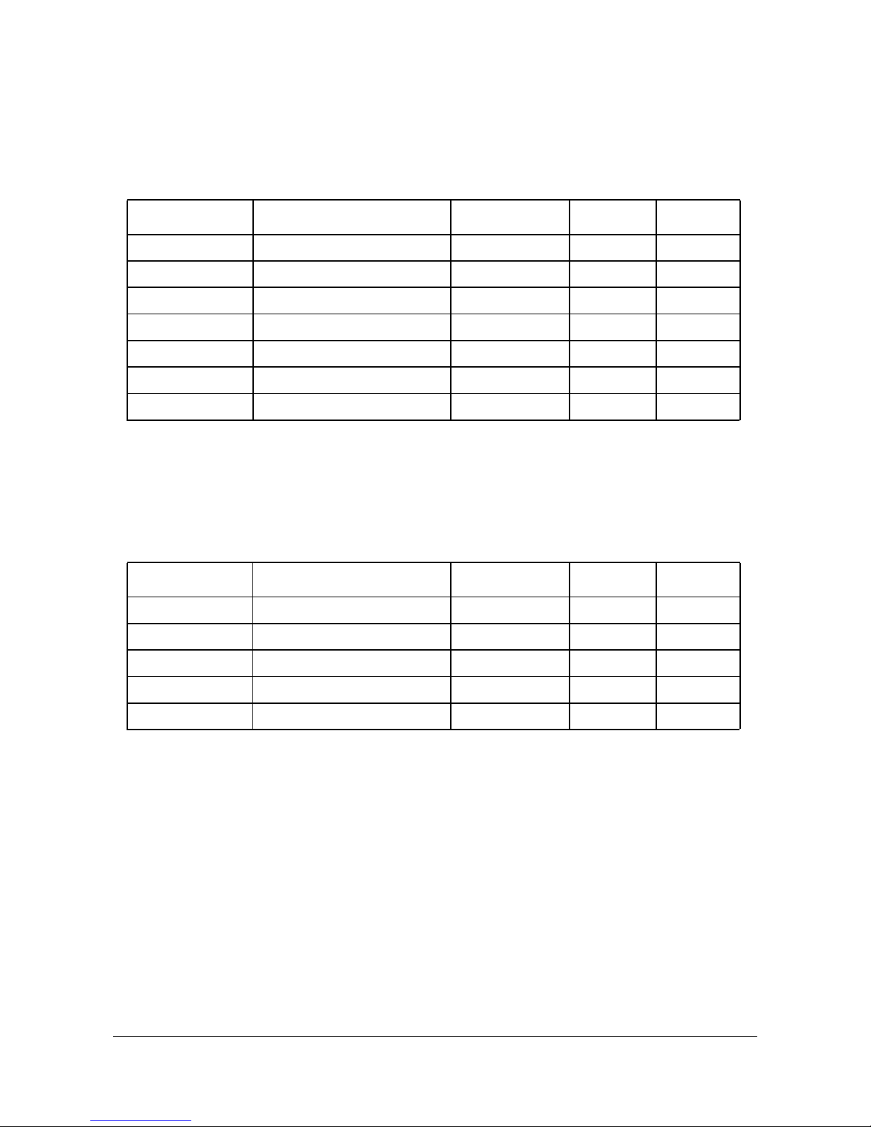
2-1-3 Factory Data by Mode
2-1-3(A) UPD64083 : TV-AV
ITEM
VAPGAIN
VAPINV
YPFP
YPFG
4
16
3
9
TV/VIdeo/S-Video/Component1,2(SD)
4
16
3
9
4
16
3
9
4
16
3
9
Component1,2(HD) PC DVI
ITEM
CONTRAST
BRIGHTNESS
PEAKING
CORING
LUMA DELAY
HPLL SPEED
YUV CONTRAST
YUV BRIGHTNESS
YUV SATCB
YUV SATCR
YUV TINT
SATURATION
TINT
TV/VIdeo/S-Video/Component1,2(SD)
43
27
5
0
255
1
29
68
42
42
3
2000
32
43
27
5
0
255
1
29
68
42
42
3
2000
32
Component1,2(HD) PC DVI
2-1-3(B) VPC3230 : TV-COMP
43
27
5
0
255
1
29
68
42
42
3
2000
32
43
27
5
0
255
1
29
68
42
42
3
2000
32
Alignment and Adjustments
Samsung Electronics 2-3
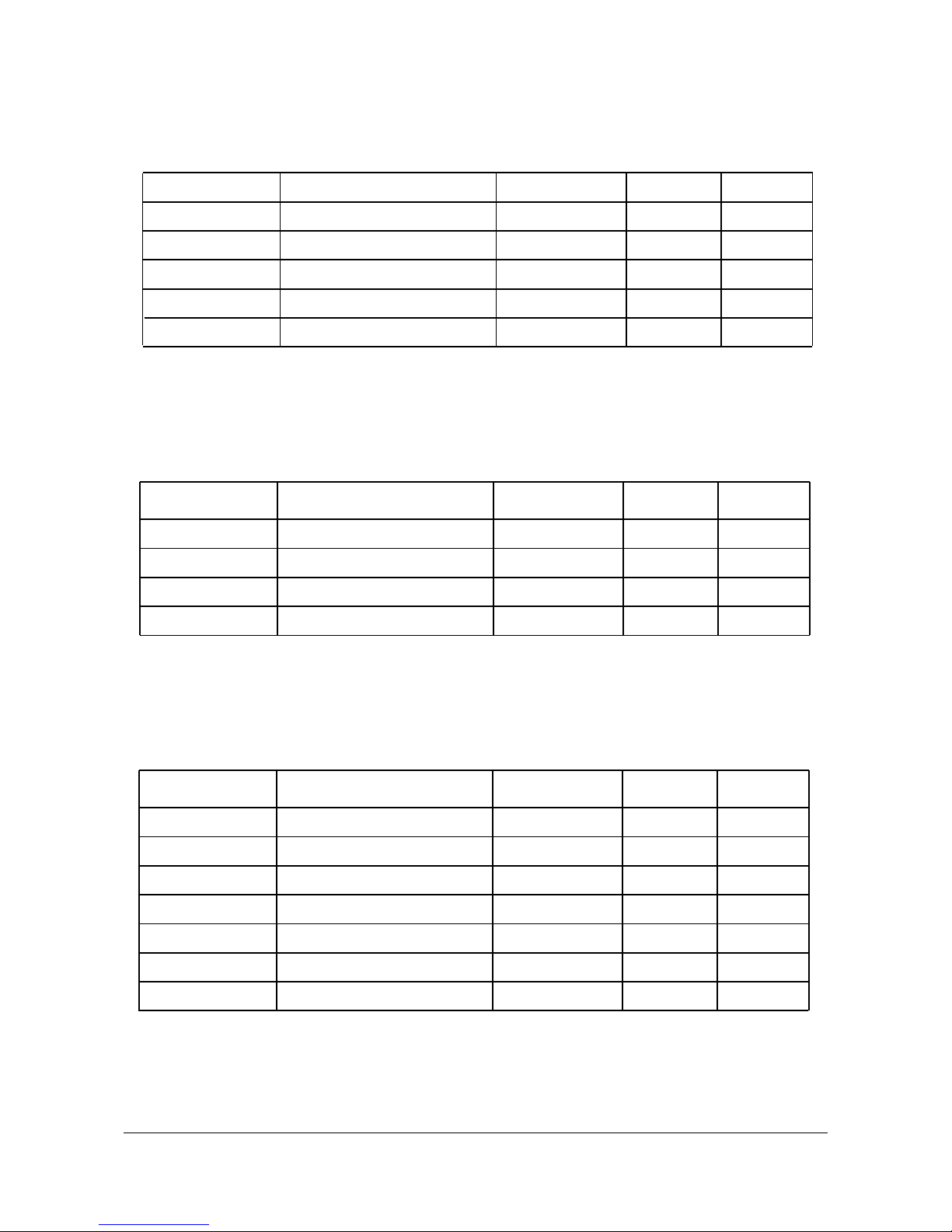
2-1-3(C) VPC3230(S) TV COMP
2-1-3(D) FLI2200 : TV-COMP
ITEM
PIP CONTRAST
PIP BRIGHTNESS
YUV CONTRAST
YUV BRIGHTNESS
LUMA DELAY
H POSITION
V POSITION
TV/VIdeo/S-Video/Component1,2(SD)
43
27
29
68
255
0
0
Component1,2(HD) PC DVI
43
27
29
68
255
0
0
43
27
29
68
255
0
0
43
27
29
68
255
0
0
ITEM
Y CLAMP
C CLAMP
Y DELAY
C DELAY
MOTION DETECT
TV/VIdeo/S-Video/Component1,2(SD)
0
512
4
11
48
Component1,2(HD) PC DVI
0
512
4
11
48
0
512
4
11
48
0
512
4
11
48

Alignment and Adjustments
2-4 Samsung Electronics
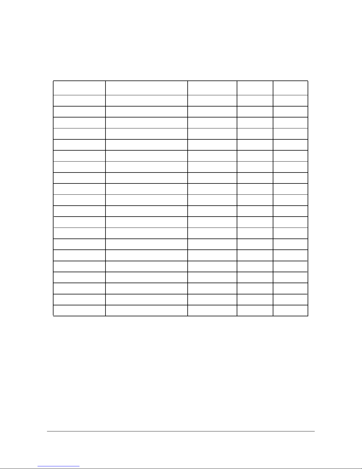
2-1-3(E) ASI500 I : ALL (EXCEPT SUB CONT/BRIGHT)
ITEM
R CONTRAST
G CONTRAST
B CONTRAST
R BRIGHTNESS
G BRIGHTNESS
B BRIGHTNESS
TEXT ALPHA
TEXT THRESHOLD
FILTER ML
FILTER MR
FILTER FR
FILTER MC
FILTER UC
FILTER LC
FILTER YPASS
R GAMMA
G GAMMA
B GAMMA
H POSITION
V POSITION
H SIZE
V SIZE
OVERSCAN B
OVERSCAN G
OVERSCAN R
TV/VIdeo/S-Video/Component1,2(SD)
32
32
32
0
0
0
1
7
0
0
0
16
0
0
0
32
32
32
0
0
0
0
63
63
63
Component1,2(HD) PC DVI
32
32
32
0
0
0
1
7
0
0
0
16
0
0
0
32
32
32
0
0
0
0
63
63
63
32
32
32
0
0
0
1
7
0
0
0
16
0
0
0
32
32
32
0
0
0
0
63
63
63
32
32
32
0
0
0
1
7
0
0
0
16
0
0
0
32
32
32
0
0
0
0
63
63
63
Alignment and Adjustments
Samsung Electronics 2-5
2-1-3(F) ASI500 II : ALL
ITEM
PIP R CONT
PIP G CONT
PIP B CONT
PIP R BRIGHT
PIP G BRIGHT
PIP B BRIGHT
PIP FILTER LC
PIP FILTER ML
PIP FILTER MR
PIP FILTER UC
TV/VIdeo/S-Video/Component1,2(SD)
32
32
32
0
0
0
0
0
0
0
Component1,2(HD) PC DVI
32
32
32
0
0
0
0
0
0
0
32
32
32
0
0
0
0
0
0
0
32
32
32
0
0
0
0
0
0
0
2-1-3(G) DNIe : ALL (EXCEPT SUB BRIGHT/CONT)
ITEM
SUB BRIGHT
SUB CONT
NR SCALE MAX
NR SCALE MIN
DE GAIN COR
DE GAIN CLIP
CE UPPER
CE CUTOFF
CE GAIN
WTE Y THRE
WTE C THRE
SYNC MODE
PATT SEL
TV/VIdeo/S-Video/Component1,2(SD)
0
0
52
18
3
60
240
64
48
230
2
1
0
Component1,2(HD) PC DVI
0
0
48
16
3
60
240
64
48
230
2
1
0
0
0
48
16
3
60
240
64
48
230
2
1
0
0
0
48
16
3
60
240
64
48
230
2
1
0
Alignment and Adjustments
2-6 Samsung Electronics
RED CONPENSA
BLUE CONPENSA
WTE GAIN
RAST VSIZE
RAST HSIZE
SHARP OFFSET
616
616
58
1023
895
0
616
616
58
1023
895
0
616
616
58
1023
895
0
616
616
58
1023
895
0
ITEM
GAIN-SEL
CR GAIN
CB GAIN
YG GAIN
TV/VIdeo/S-Video/Component1,2(SD)
1
7
7
1
1
7
7
1
Component1,2(HD) PC DVI
2-1-3(H) CXA2151HD : COMP-PC
1
7
7
1
1
7
7
1
2-1-3(I) AD9883 : COMP-PC
ITEM
R GAIN
G GAIN
B GAIN
R, CR OFFSET
G, Y OFFSET
B, CB OFFSET
AUTO COLOR
TV/VIdeo/S-Video/Component1,2(SD)
142
142
142
60
48
64
-
Component1,2(HD) PC DVI
142
142
142
60
48
64
-
142
142
142
54
54
54
-
142
142
142
54
54
54
-
AUTO COLOR : Automatic white balance adjustment in pc mode and component(HD) mode.
Alignment and Adjustments
Samsung Electronics 2-7
2-1-3(J) LOGIC : ALL (EXCEPT DRIVE/CUTOFF)
ITEM
R DRIVE
G DRIVE
B DRIVE
R CUTOFF
G CUTOFF
B CUTOFF
GAMMA
GTS SET
ERD MODE
RANDOM NOISE
DIFF FILTER
APC
APC SET
APC VALUE
ACTIVE VPOS
ACTIVE HPOS
VSYNC POS
HSYNC POS
VSYNC WIDTH
HSYNC WIDTH
TV/VIdeo/S-Video/Component1,2(SD)
140
130
120
0
0
0
1
0
2
0
1
1
0
127
12
19
3
32
2
12
Component1,2(HD) PC DVI
140
130
120
0
0
0
1
0
2
0
1
1
0
127
12
19
3
32
2
12
140
130
120
0
0
0
1
0
2
0
1
1
0
127
12
19
3
32
2
12
140
130
120
0
0
0
1
0
2
0
1
1
0
127
12
19
3
32
2
12

Alignment and Adjustments
2-8 Samsung Electronics
ITEM
LOG PATTERN
LOG HIGH LEVEL
LOG LOW LEVEL
ASI COLOR BAR
TV/VIdeo/S-Video/Component1,2(SD)
0
255
0
0
Component1,2(HD) PC DVI
2-1-3(K) TP LOG-ASI : ALL
0
255
0
0
0
255
0
0
0
255
0
0
2-1-3(L) OPTION : ALL
ITEM
PIX SHIFT
SHIFT TEST
PIX NUMBER
SHIFT LINE
SHIFT TIME
NUMBER RANGE
LINE RANGE
COUNTRY
TEMP PROTECT
DNIe DEMO
DNIe THROUGH
VIDEO MUTE
IRC AFN
LANGUAGE
CUSTOMER
TUNER
PILOT HIGH
PILOT LOW
RESET
TV/VIdeo/S-Video/
Component1,2(SD)
0
0
1
1
4
4
4
0
0
0
0
10
0
0
0
1
21
16
-
Component1,2(HD) PC DVI
0
0
1
1
4
4
4
0
0
0
0
10
0
0
0
1
21
16
-
0
0
1
1
4
4
4
0
0
0
0
10
0
0
0
1
21
16
-
0
0
1
1
4
4
4
0
0
0
0
10
0
0
0
1
21
16
-
Adjustment
0:OFF 1:RF,Video,S-Video,Component1,2 2:PC 3:ALL
0:minute 1:second
Number of pixels that shift left/right
Number of lines that shift up/down
Time set during shift test
Shift range
Shift range
0:Korean 1:America 2:Japan
Not used
0:OFF 1:ON
0:Not through 1:Through
Unit:100mese
0:General American mode
1:Military American mode
0:English 1:French 2:Spanish
0:CE 1:VMB
0:1 TUNER 1:2 TUNER
Stereo ↔ mono boundary value
Stereo ↔ mono boundary value
Customer settings reset
Alignment and Adjustments
Samsung Electronics 2-9
Alignment and Adjustments
2-2 WHITE Balance Coordinates
2-2-1 SPN4235 White Balance Adjustment
1. W/B Adjustment is required for the following four modes: DVI → DTV → PC → RF
2. Adjustment Method (DVI, DTV, PC : VG828, RF : Adjust RF signals to match the
Toshiba pattern (in-house signal)
! Adjust the target set by adjusting the panel logic and the video DNIe adjustment register in
register in order to determine the referential W/B of the panel with a DVI input, which
is the full digital path.
@ For DTV adjustment, adjust the adjustment register of AD9883 to align the DTV signal
to the DNIe and logic panel value which was fixed with a DVI adjustment so that they are
in effect considered to be the same signals. (At this time, do not adjust the gain of
AD9883
→ the Highlight W/B does not need to be adjusted since its deviation falls
within valid distribution range.)
# PC adjustment is same as DTV adjustment. (The offset can be applied to the values
obtained through DTV adjustment. However, additional adjustment is required for
Y, Cb, and Cr of DTV since PC processes R, G, and B signals.)
$ RF adjustment is performed with the Toshiba pattern (in-house signal) and differs
from the VG828 signals in the above three modes. Hence, it should be performed with
the same method of ! DVI adjustment.
❈ Thus, Micom saves the W/B data separately for each memory mode of the block
(See the block diagram given below) during W/B adjustment.
Adjustment Reg
Adjustment Reg
Adjustment Reg
Memory mode
Memory mode
Memory mode
level
level
Micom can memorize the four modes
separately. However, under the current
adjustment guidelines, DTV and PC are
memorized with the same value during
DVI adjustment and RF is memorized
with a separate value.
Alignment and Adjustments
2-10 Samsung Electronics
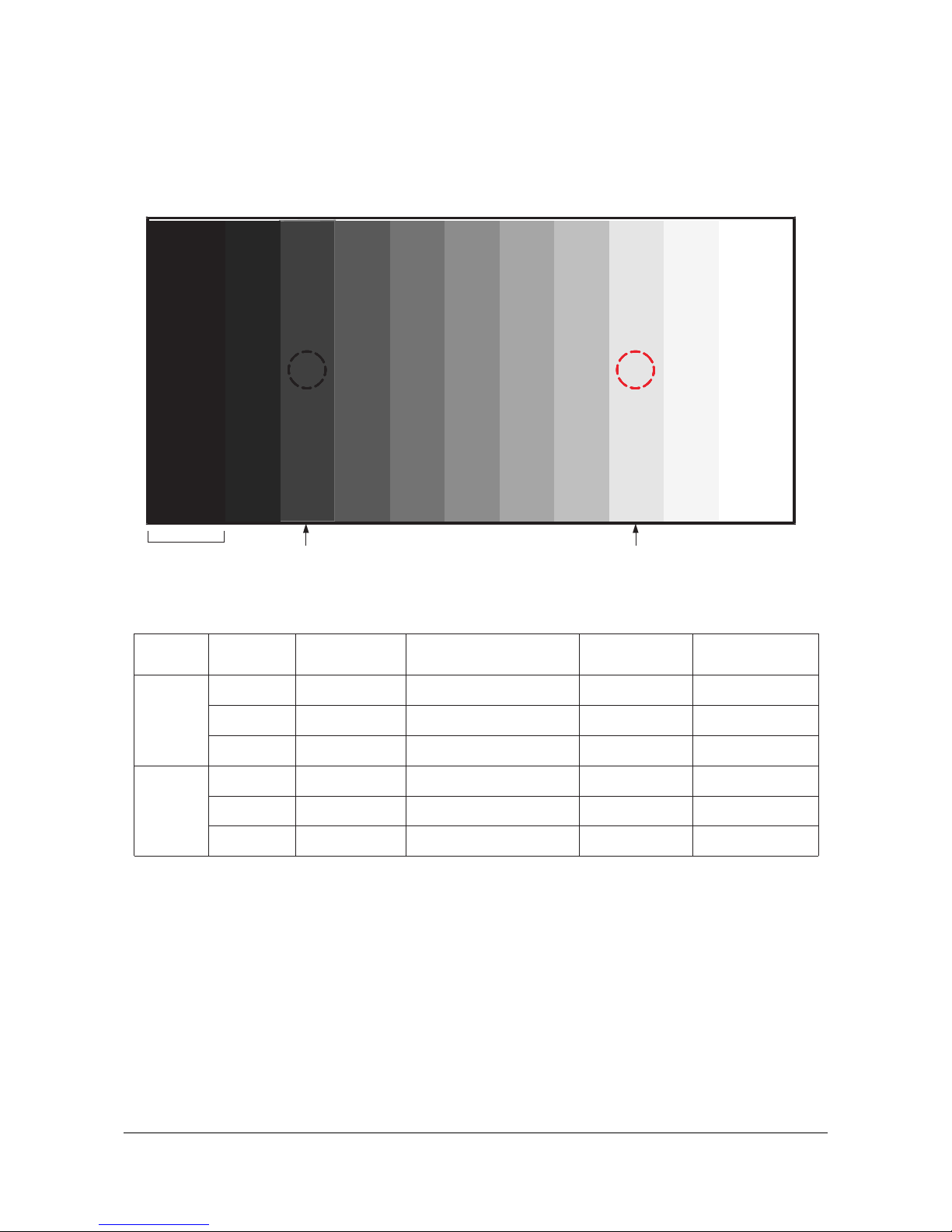
2-2-2 White Balance Coordinates by Mode
DVI
DTV COMPONENT
(480P, 720P,1080i
)
PC VIDEO
H/L
x 285 285 290 285
y 290 290 305 300
Y(fL) 32.0 33.0 17.6 33.0
L/L
x 285 285 290 285
y 295 290 300 295
Y(fL) 1.3 1.2 1.0 1.4
PedestalLevel Low Light
measure point
High Light
measure point
= Pattern Used in Adjustment : 10 Steps Grayscalepattern

Alignment and Adjustments
Samsung Electronics 2-11
2-3 Voltage Adjustment
Turning the variable resistor(VR) adjusts voltage.
CN804
CN800S
CN801
CN803
CN802
N805
N806
N812
T(VS)
T:TestPoint
T(VSCAN)
T(VSET)
T(VA)
T(VG)
T(STB_5V)
T(VE)
VR4
VSET
VR6
VSCAN
VR5
VE
VR1
VS
VR7
VA
VR3
D5V
VR2
Vstb
VR: Variable Resistor
SMPS
OUTPUT Voltage( V)
VA
See the labels attached
on the base chassis.
VSCAN(VSC)
VS
VE
VSET
D5V
+5V
STB_5V
+5V
VG
+15V

2-12 Samsung Electronics
MEMO
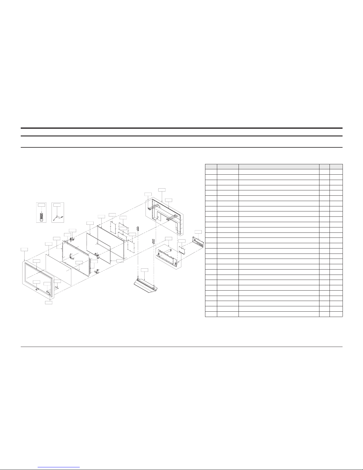
3. Exploded View & Parts List
3-1 PDP4298EDX/SMS
Exploded View & Parts List
Samsung Electronics 3-1
T0268T0074
T0915
T0911
T0912
T0054
T0914
T0003
T0003
T0057
T0022
T0098
T0061
T0913
T0918
T0918
T0044
T0033
T0046
T0916
T0001
T0112
T0555
M0165
T0008
T0032
T0037
T0144
Yon can search for the updated part code through ITSELF web site.
URL:http://itself.sec.samsung.co.kr
Loc.No. Code No. Description;Specification Q'ty S.N.A
M0165 BN94-00494E ASSY PCB MISC-2 TUNER DIGITAL;PDP4294X/S 1
T0001 BN96-00314A ASSY COVER P-BACK;42P3H,AL 5052,T1.2 1
T0003 BN96-00737C ASSY COVER P-FRONT;PDP4298,AKAI,HIPS V0, 1
T0003 BN64-00206A CABINET FRONT;PDP4294,HIPS V0,GRAY 1 S.N.A
T0008 BN96-00313B ASSY COVER P-BACK SUB;PS42P3S,AL5052 T1. 1 S.N.A
T0022 BP64-00045D KNOB-CONTROL;PDP4294,ABS,HB,SV-704P,AKAI 1 S.N.A
T0032 BN96-00257A ASSY PDP P-PBA,Y MAIN;LJ92-00636A,SPD-42 1
T0033 BN96-00256A ASSY PDP P-PBA,X MAIN;LJ92-00635A,SPD-42 1
T0037 BN96-00710A ASSY PDP P-PBA,L MAIN;M3,S42SD-YD04,42SD 1
T0044 BN96-00709A ASSY PDP MODULE P;M3,S42SD-YD03,D54A,S2. 1
T0046 BN96-00249A ASSY PDP P-SMPS;,42P3S/50P3H,42SD/50HD,4 1
T0054 BN64-00122A SCREEN-EMI,FILTER;FILTER,42P3,984*584,T3 1
T0057 AA64-03228A BADGE-BRAND;54J7,AL,T1.5,12,51.2,BLACK,A 1 S.N.A
T0061 BN64-00074B WINDOW-REMOTE;42P3S,PMMA,,,,,,CLEAR 1 S.N.A
T0074 BN59-00347C REMOCON;TM63,ALEXANDER,47,SVM-3012,DO 1
T0098 BN94-00494B ASS'Y PCB MISC-CONTROL;SPN4235,D54B,ALEX 1
T0112 BN63-00529A COVER-BACK;42P3H,AL 3031,T1.2,DGM-5810 1 S.N.A
T0144 BN96-00137B ASSY COVER P-STAND BASE;PDP-4295ED,AKAI, 1
T0268 3903-000085 CBF-POWER CORD;DT,US,BP3/YES,I(IEC C13/C 1
T0555 BN96-00286C ASSY MISC P-BRACKET TERMINAL;P3,U.S.A 1 S.N.A
T0911 BN61-00244H BRACKET-FILTER TOP ASSY;42P3S,AL5052,T1. 1 S.N.A
T0912 BN61-00245H BRACKET-FILTER SIDE L;42P3S,AL5052,1.2 1 S.N.A
T0913 BN61-00309E BRACKET-FILTER SIDE R;42P3S,AL5052,1.2 1 S.N.A
T0914 BN61-00246G BRACKET-FILTER BOTTOM ASSY;42P3S,AL5052, 1 S.N.A
T0915 BN61-00141A HOLDER-MODULE;42P3,AL,DIECASTING 4 S.N.A
T0916 BN61-00202A BRACKET-HANDLE;42P3S,AL5052,T1.5,DGM-S81 2 S.N.A
T0918 AA60-00110G SPACER-FILTER;42P3,P/U FROM,560,5,6 1 S.N.A
T0918 AA60-00110J SPACER-FILTER;50P3,P/U Form,20.0,2.0,5.0 2 S.N.A

Electrical Parts List
Samsung Electronics
4-1
4. Service Item
4-1 Assy Board & Part List for Service
No Description Code No Specification
ASSY PDP P-MODULE BN96-00709A
M3,S42SD-YD03,D54A,S2.0,1015 x 613,852 x 480,NTSC/PAL,42",ASIC
①
ASSY PDP P-PBA,L MAIN BN96-00710A M3,S42SD-YD04,42SD S2.0,79mm logic board,LJ92-00817A
②
ASSY PDP P-PBA,L BUFF(E) BN96-00253A
LJ92-00632A,SPD-42P3,D54A,42",ALEXANDER ,SD,SDI CODE
③
ASSY PDP P-PBA,L BUFF(F) BN96-00254A
LJ92-00633A,SPD-42P3,D54A,42",ALEXANDER ,SD,SDI CODE
④
ASSY PDP P-PBA,L BUFF(G) BN96-00255A
LJ92-00634A,SPD-42P3,D54A,42",ALEXANDER ,SD,SDI CODE
⑤
ASSY PDP P-PBA,X MAIN BN96-00256A
LJ92-00635A,SPD-42P3,D54A,42",ALEXANDER ,SD,SDI COD
⑥
ASSY PDP P-PBA,Y MAIN BN96-00257A
LJ92-00636A,SPD-42P3,D54A,42",ALEXANDER ,SD,SDI CODE
⑦
ASSY PDP P-PBA,Y BUFF(UP) BN96-00258A
LJ92-00637A,SPD-42P3,D54A,42",ALEXANDER ,SD,SDI CODE
⑧
ASSY PDP P-PBA,Y BUFF(DOWN) BN96-00259A
LJ92-00638A,SPD-42P3,D54A,42",ALEXANDER ,SD,SDI CODE
⑨
ASSY PDP P-SMPS BN96-00249A
42P3S/50P3H,42SD/50HD,445*245,42MM_MAX,90V~264V,NTSC/PAL,SEMCO
⑩
ASSY PCB MISC-2 TUNER DIGITAL BN94-00494E PDP4294X/SMS,D54B,SAMS CLUB
⑪
ASSY PCB MISC-2 TUNER ANALOG BN94-00421A SPD-50P3H,D57A
⑫
ASSY PCB MISC-CONTROL BN94-00494B SPN4235,D54B,ALEX
SCREEN-EMI,FILTER BN64-00122A FILTER,42P3,984*584,T3.0,0.1ohm,T47%

Electrical Parts List
4-2
Samsung Electronics
Yon can search for the updated part code through ITSELF web site.
URL:http://itself.sec.samsung.co.kr
4-2 PDP4298EDX/SMS
Loc.No. Code No. Description;Specification Q'ty
CIS3 BN40-00007A TUNER;TCPN9081PC27D,TCPN9081PC27D,45.75M 1
CIS3 BN40-00017A TUNER;TCLN9081PC27S(S),NTSC,181CH,45.75M 1
M0165 BN94-00494E ASSY PCB MISC-2 TUNER DIGITAL;PDP4294X/S 1
M0166 BN94-00421A ASSY PCB MISC-2 TUNER ANALOG;SPD-50P3H,D 1
T0001 BN96-00314A ASSY COVER P-BACK;42P3H,AL 5052,T1.2 1
T0003 BN96-00737C ASSY COVER P-FRONT;PDP4298,AKAI,HIPS V0, 1
T0014 BN96-00259A ASSY PDP P-PBA,Y BUFF(DOWN);LJ92-00638A, 1
T0032 BN96-00257A ASSY PDP P-PBA,Y MAIN;LJ92-00636A,SPD-42 1
T0033 BN96-00256A ASSY PDP P-PBA,X MAIN;LJ92-00635A,SPD-42 1
T0037 BN96-00710A ASSY PDP P-PBA,L MAIN;M3,S42SD-YD04,42SD 1
T0038 BN96-00253A ASSY PDP P-PBA,L BUFF(E);LJ92-00632A,SPD 1
T0039 BN96-00254A ASSY PDP P-PBA,L BUFF(F);LJ92-00633A,SPD 1
T0040 BN96-00255A ASSY PDP P-PBA,L BUFF(G);LJ92-00634A,SPD 1
T0044 BN96-00709A ASSY PDP MODULE P;M3,S42SD-YD03,D54A,S2. 1
T0046 BN96-00249A ASSY PDP P-SMPS;,42P3S/50P3H,42SD/50HD,4 1
T0048 BN96-00258A ASSY PDP P-PBA,Y BUFF(UP);LJ92-00637A,SP 1
T0054 BN64-00122A SCREEN-EMI,FILTER;FILTER,42P3,984*584,T3 1
T0074 BN59-00347C REMOCON;TM63,ALEXANDER,47,SVM-3012,DO 1
T0098 BN94-00494B ASS'Y PCB MISC-CONTROL;SPN4235,D54B,ALEX 1
T0144 BN96-00137B ASSY COVER P-STAND BASE;PDP-4295ED,AKAI, 1
T0175 BN96-00201D ASSY SPEAKER P;8ohm,PSN4294,One-packing, 1
T0568 BN39-00338A CBF IF;D56A/PS42P3S,1P,1365#26,50MM,BLAC 1

Circuit Operation Description
Samsung Electronics 5-1
5. Circuit Description
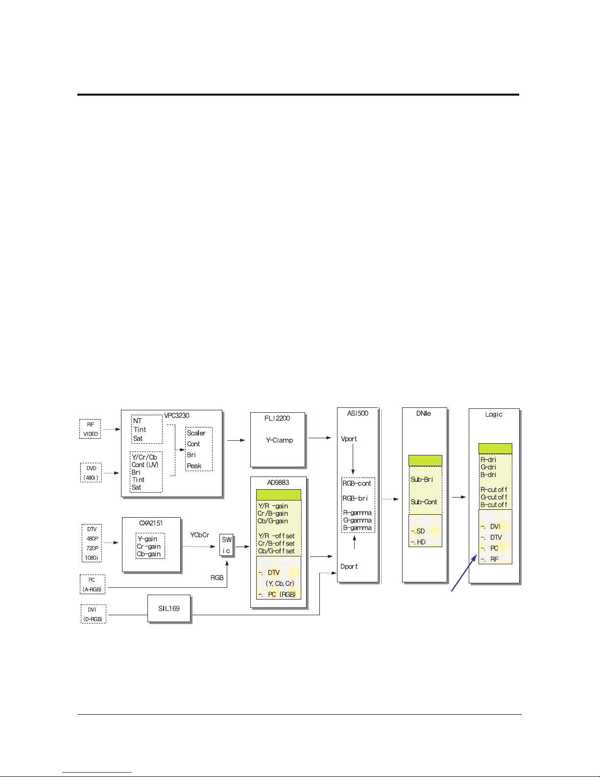
5-1 BLOCK DIAGRAM
Input
Data
Processor
Data
controller
DRAM
Driver
Timing
controller
852x480 Pixels
852x3x480 Cells
PDP PANEL
Row
Driver
Y-P ulse
Generator
Column Driver
X-P ulse
Generator
Power Supply
AC Power
Source
(110/220V)
LVDS
Display
Data
Driver
Timing
Scan
Timing
A/D
Converter
Image
Scalar
Micom
Image
Enhancer
LOGIC B’d
ANAL OG B’d
POWER B’d
B’d
B’d
clock:
60MHz
clock:
27MHz
clock:
20MHz
40MHz
DIGITAL B’d
Video
Decoder
Deinterlac
er
TMDS
Receiver
Video
S/W
Audio
Processor
Comb
Filter
SUB
Tuner
MAIN
Tuner
Y Driver
X Driver

Circuit Operation Description
5-2 Samsung Electronics
5-2 WIRE DIAGRAM

Circuit Operation Description
Samsung Electronics 5-3
5-3 POWER SUPPLY
5-3-1 Block Diagram
(+ 95V)
(+ 110V)
78V
MAG-AMP
85

Circuit Operation Description
5-4 Samsung Electronics
5-3-2 Circuit Description
1. Outline (PDP42inch SMPS)
Considering various related conditions, the switching regulator with good fficiency and allowing for its
small size and light weight was used as the power supply for PDP 50inch (Alexander), VS requiring high
power consumption used Asymmetrical Half Bridge converter and flyback converter and other high voltage (VSCAN, VSET, VE) used DC/DC converter. To comply with the international harmonics standards
and improve the power factor, active PFC(Power Factor Correction) was used to rectify AC input into
+400V DC output, which in turns used as input to the switching regulator.
2. INPUT
The power supply shall be capable of supplying full rated output power over free voltage ranges that are
rated 100 VAC -240 VAC RMS nominal. Operating voltage : 90 VAC - 264 VAC
The power supply must be able to start up under peak loading at 90V AC. The power supply shall automatically recover from AC power loss. (Note that nominal voltages for test purposes are considered to be
with +/- 1.0V of nominal).
STD_5V is a SELV standby voltage that is always present when AC mains voltage present.
3. OUTPUT
This power supply is 15 output switching power supply for PDP 42inch(Alexander). The output voltage,
and current requirements for continuous operation are stated below. (table 1)
Table1. Specifications of Output Power Supplies for PDP SMPS
Output Name
VS
VA
VSCAN
VSET
VE
VG
D12V
A12V
D6V
A6V
D5V
D3.3V
12V AMP
VT
STD_5V
Output Voltage
+75V ~ 100V (89V)
+65V ~ 80V (78V)
+65V ~ 100V (75V)
+80V ~ 10V (95V)
+100V ~ 120V (110V)
+15V
+12V
+12V
+6V
+6V
+5V
+3.3V
+12V
+33V
+5V
Output Current(Max)
4.5A
0.6A
0.1A
0.1A
0.1A
1.5 A
0.1A
0.3A
0.1A
0.1A
1.0A
4.5A
1.7A
0.003A
0.6A
Using in PDP driving
Sustain Voltage of Drive Board
Address Voltage of Drive Board
Driving Voltage of Fet
IC Driving Voltage of Logic Board
Amp Voltage of Audio Board
Stand-by for Remote Control

Circuit Operation Description
Samsung Electronics 5-5
1) Over voltage Protection
SMPS has an over voltage detection circuit as well as a circuit which keeps a constant level of voltage.
It is designed so that when an Over Voltage occurs in any part it does not affect another output part.
SMPS cuts off Over Voltage in latch mode. The following tagle gives te Over Voltage protection
specifications.
Table2. Over voltage Protection.
Parameter
VS(85V)
VA(75V)
D6V
D3.3V
Min
100 ~
94 ~
8.2 ~
4.7 ~
Unit
V
V
V
V
2) Short Circuit and Over current Protection.
Short-circuit of the output terminal is defined as an output impedance that is less than 300mohm.
For a given SMPS, when a VS output is short-circuited, the SMPS stops operation. Even if a short-circuit
occurs between the main output and the STD_5V, the SMPS does not fail. When the short-circuit is cleared,
it will operate normally again. Even if a short_circuit occurs when the SMPS is operating within the range
presented in Chapter 3, it will not cause a malfunction to the parts or the PCB patterns.
The following table gives Over Current protection specifications.
Table3. Over Current Protection.
Parameter
VS(85V)
VA(75V)
12V
6V
D3.3V
Min
~
~
~
~
~
Unit
A
A
A
A
A

Circuit Operation Description
5-6 Samsung Electronics
4. Function of Board
! Remote Control
Using a 250V/10A relay. The board makes remote control available.
@ Free Voltage
The Board is designed so that the input voltage can be used within 90VAC to 264VAC.
# Improvement of power factor
The SMPS has a power-factor compensation circuit so that the power-factor can be more than 0.9.
$ Protection
The SMPS has circuits which protect the product from over current, over voltage and short-circuit.
5. Part Block Diagram and Part Function.
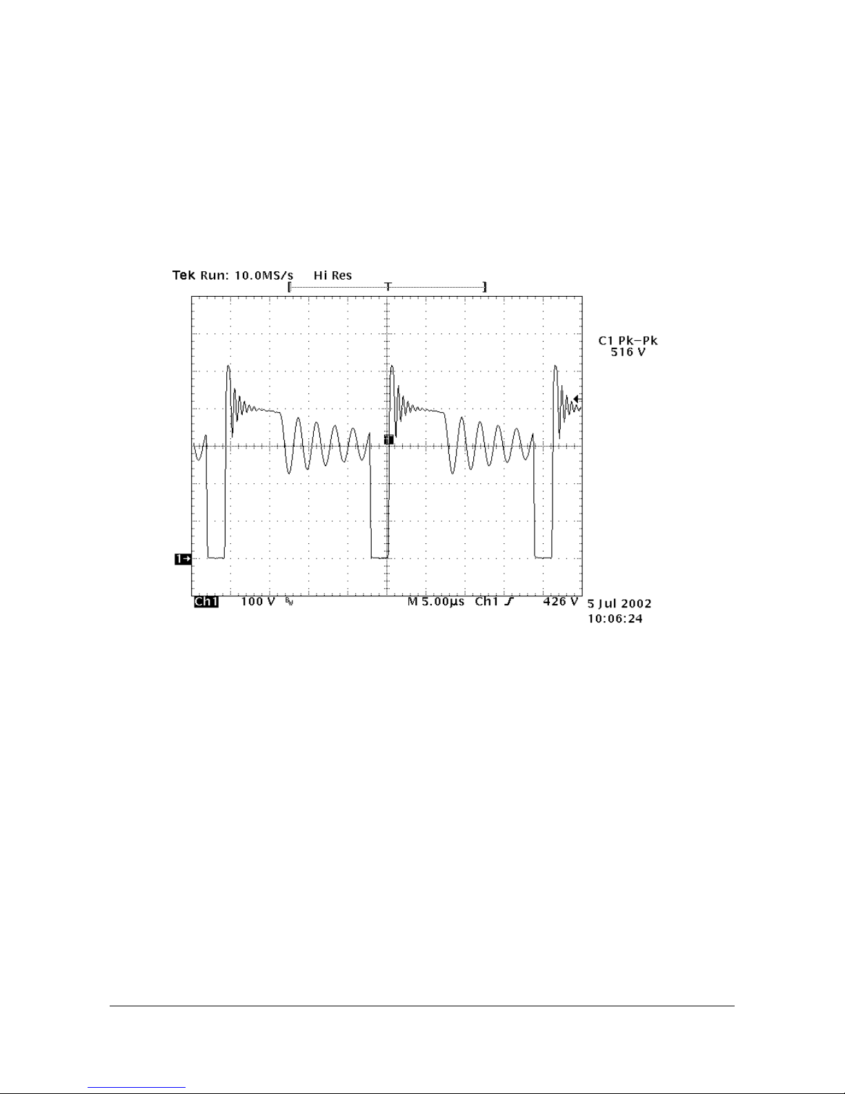
! AC-DC Converter
The AC/DC Converter converts AC input into DC voltage using a power-factor enhancement circuit.
It is designed to not only enhance the power-factor but also suppress noise. It also becomes the input
for other constant voltage parts.
Picture 1. PFC Drive FET(2SK2372) Drain pulse

Circuit Operation Description
Samsung Electronics 5-7
Picture 2. PFC Drive FET(2SK2372) Gate pulse
- Oscillator Frequency
Oscillator Frequency is determined by the values of Rt and Ct in the circuit. These values also
determine the oscillation wave tilt and the off time of frequency. Osillation frequency is obtained
using the following formula.
f
osc =
t
RAMP
=CtxRtx0.51
f
osc =
= 59.417kHz
R
t
( R59 : 1/8W 20K ) , Ct( C14 : MLCC 222 )
1
t
RAMP
1
22 20 051.**.nF
k
In the SMPS circuit, the oscillation frequency is as follows:
Circuit Operation Description
5-8 Samsung Electronics
@ Auxiliary Power Supply
The auxiliary power supply supplies power to the remote control for activating the Micom. It operates
anytime the power cord is connected to a power source and the Micom is in stand-by mode. The output
in this state is called Stand-By voltage. When the ON signal is activated from the remote control, the
main power supply of the SMPS starts operation.
Picture 3. Standby flyback Pulse.
# Implementation of Sustain Voltage
As the main part of a SMPS for PDP, sustain voltage must supply a high power, 85V/5.0A.
To comply with the specification, the Asymmetrical Half Bridge converter method was used.
At the output stage two 85V converters are connected parallel for high efficiency and reduction of system size against a single 85V converter.

Circuit Operation Description
Samsung Electronics 5-9
Picture 4. VS Drive FET(SPW17N80C3) Drain pulse
Picture 5. VS Drive FET(SPW17N80C3) Gate pulse

Circuit Operation Description
5-10 Samsung Electronics
- PWM SECTION (Pulse Width Modulator)
The PWM component of ML4824 is used. There are some items you should pay attention to.
The PWM component is synchronized with the PFC component mentioned above.
In Current Mode Operations, a PWM wave is induced via a current detection resistor or current
transformer and indicates the current that flows through the output terminal.
$ DC-DC Converter
Input to VSCAN, VSET and VE are included in the VS component.
Picture 6. VSET Pulse
Picture 7. VE Pulse

Circuit Operation Description
Samsung Electronics 5-11
Picture 8. VSCAN Pulse
Picture 9. VA Main Pulse
% Output (VA,Multi Outputs) Pulse
 Loading...