


KS57C2308/P2308/C2316/P2316 PRODUCT OVERVIEW
1-1
1 PRODUCT OVERVIEW
OVERVIEW
The KS57C2308/C2316 single-chip CMOS microcontroller has been designed for high performance using
Samsung's newest 4-bit CPU core, SAM47 (Samsung Arrangeable Microcontrollers).
With features such as LCD direct drive capability, 8-bit timer/counter, and serial I/O, the KS57C2308/C2316 offer
an excellent design solution for a wide variety of applications that require LCD functions.
Up to 40 pins of the 80-pin QFP package can be dedicated to I/O. Six vectored interrupts provide fast response
to internal and external events. In addition, the KS57C2308/C2316's advanced CMOS technology provides for
low power consumption and a wide operating voltage range.
OTP
The KS57C2308/C2316 microcontroller is also available in OTP (One Time Programmable) version,
KS57P2308/P2316. KS57P2308/P2316 microcontroller has an on-chip 8/16-Kbyte one-time-programmable
EPROM instead of masked ROM. The KS57P2308/P2316 is comparable to KS57C2308/C2316, both in function
and in pin configuration.

PRODUCT OVERVIEW KS57C2308/P2308/C2316/P2316
1-2
FEATURES
Memory
– 512 × 4-bit RAM
– 8 K × 8-bit ROM (KS57C2308/P2308)
– 16 K × 8-bit ROM (KS57C2316/P2316)
I/O Pins
– Input only: 8 pins
– I/O: 24 pins
– Output: 8 pins sharing with segment driver
outputs
LCD Controller/Driver
– Maximum 16-digit LCD direct drive capability
– 32 segment, 4 common pins
– Display modes: Static, 1/2 duty (1/2 bias),
1/3 duty (1/2 or 1/3 bias), 1/4 duty (1/3 bias)
8-Bit Basic Timer
– Programmable interval timer
– Watchdog timer
8-Bit Timer/Counter 0
– Programmable 8-bit timer
– External event counter
– Arbitrary clock frequency output
– Serial I/O interface clock generator
Watch Timer
– Real-time and interval time measurement
– Four frequency outputs to BUZ pin
– Clock source generation for LCD
8-Bit Serial I/O Interface
– 8-bit transmit/receive mode
– 8-bit receive only mode
– LSB-first or MSB-first transmission selectable
– Internal or external clock source
Bit Sequential Carrier
– Support 16-bit serial data transfer in arbitrary
format
Interrupts
– Three internal vectored interrupts
– Three external vectored interrupts
– Two quasi-interrupts
Memory-Mapped I/O Structure
– Data memory bank 15
Two Power-Down Modes
– Idle mode (only CPU clock stops)
– Stop mode (main or sub system oscillation stops)
Oscillation Sources
– Crystal, ceramic, or RC for main system clock
– Crystal or external oscillator for subsystem clock
– Main system clock frequency: 4.19 MHz (typical)
– Subsystem clock frequency: 32.768 kHz
– CPU clock divider circuit (by 4, 8, or 64)
Instruction Execution Times
– 0.95, 1.91, 15.3 µs at 4.19 MHz (main)
– 122 µs at 32.768 kHz (subsystem)
Operating Temperature
– – 40 °C to 85 °C
Operating Voltage Range
– 1.8 V to 5.5 V
Package Type
– 80-pin QFP
KS57C2308/P2308/C2316/P2316 PRODUCT OVERVIEW
1-3
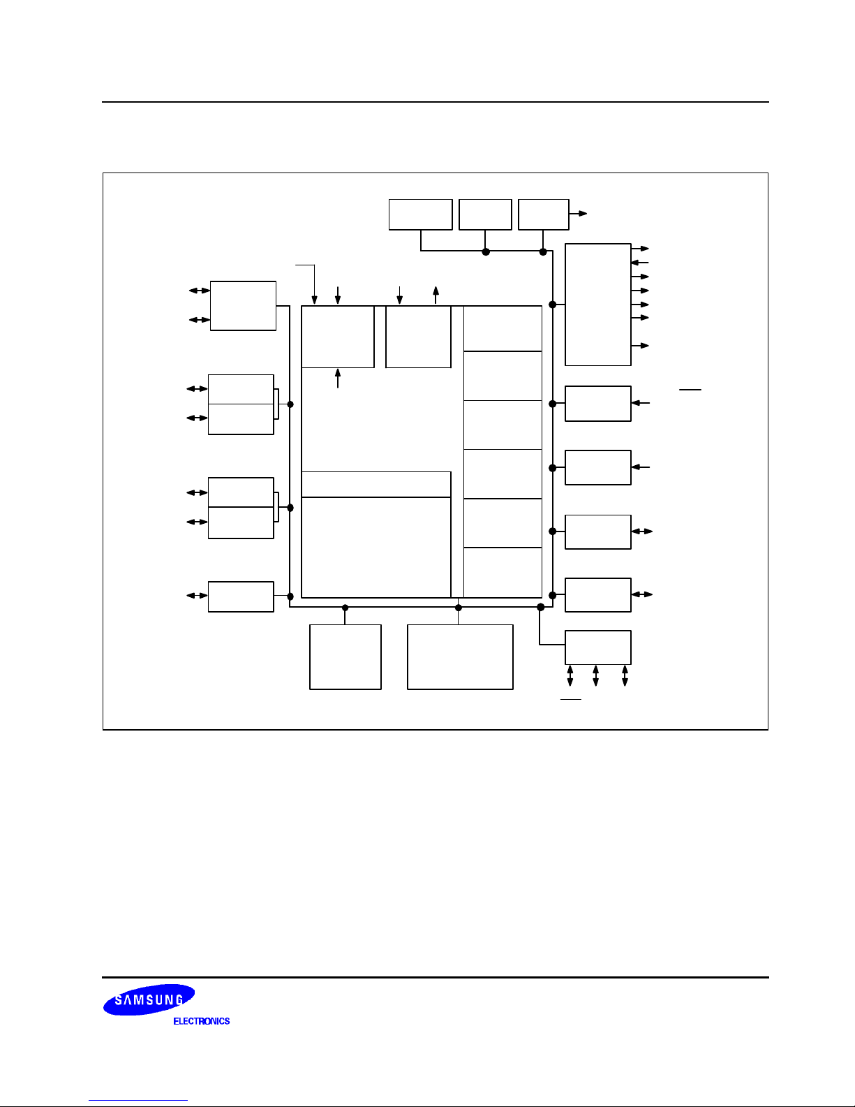
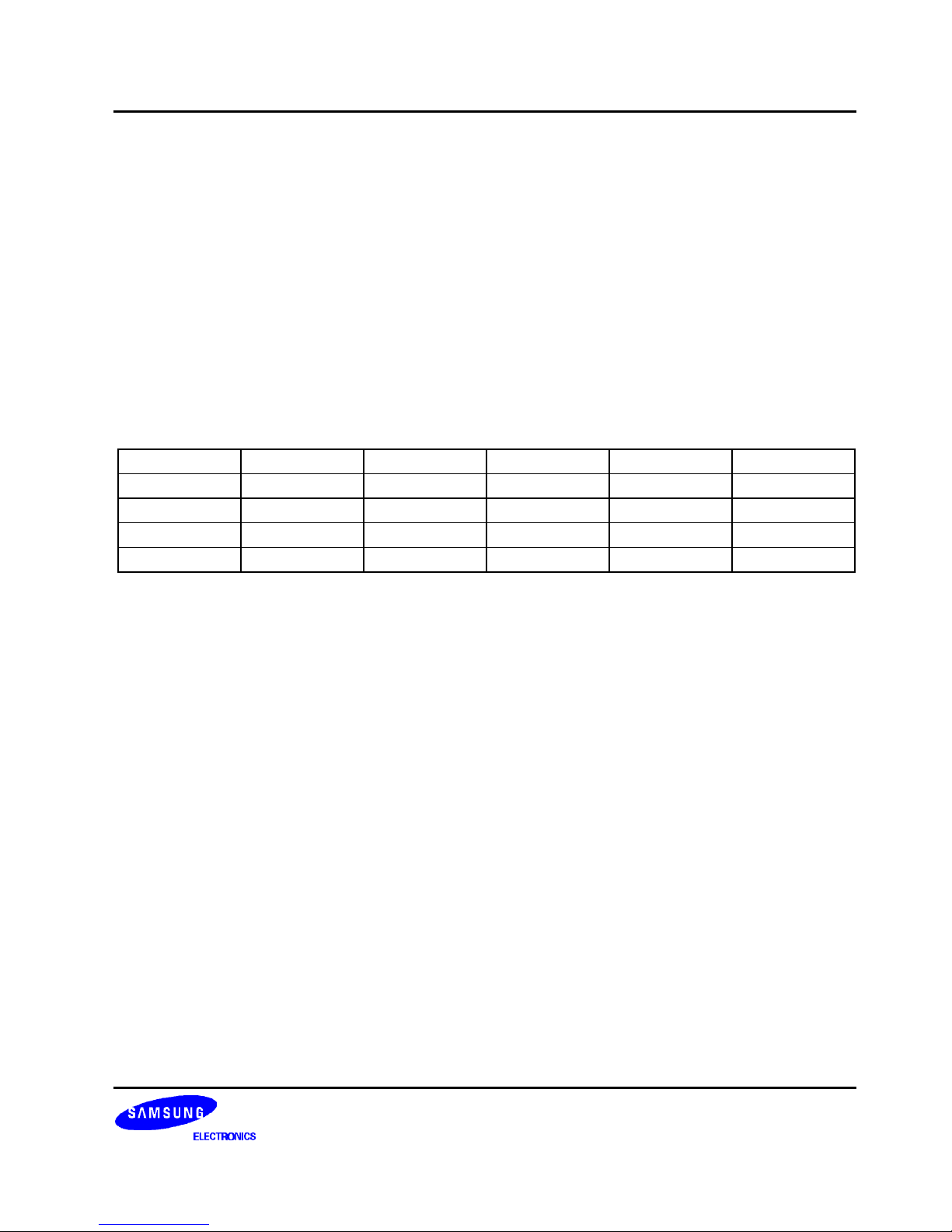
BLOCK DIAGRAM
Interrupt
Control
Block
Instruction
Register
Program
Counter
Program
Status Word
Stack
Pointer
Arithmetic and Logic Unit
Instruction Decoder
Clock
RESET
X
IN
XT
IN
Internal
Interrupts
INT0, INT1,INT2
P3.0/LCDCK
P3.1/LCDSY
P3.2
P3.3
I/O Port 3
512 x 4-Bit
Data
Memory
8/16-Kbyte
Program
Memory
LCD Drive/
Controller
BIAS
VLC0-VLC2
LCDCK/P3.0
LCDSY/P3.1
COM0-COM3
SEG0-SEG23
P8.0-P8.7/
SEG24-SEG31
P2.3/BUZ
X
OUT
XT
OUT
P6.0-P6.3/
KS0-KS3
I/O Port 6
P7.0-P7.3/
KS4-KS7
I/O Port 7
P4.0-P4.3
I/O Port 3
P5.0-P5.3
I/O Port 4
8-Bit Timer/
Counter 0
P1.3/TCL0
P2.0/TCLO0
P8.0-P8.7/
SEG24-SEG31
I/O Port 8
P1.0/INT0
P1.1/INT1
P1.2/INT2
P1.3/TCL0
Input Port 1
P2.0/TCLO0
P2.1
P2.2/CLO
P2.3/BUZ
I/O Port 2
Basic
Timer
4-Bit
Accumulator
FLAGS
P0.0/INT4
P0.1/SCK
P0.2/SO
P0.3/SI
I/O Port 0
Serial I/O
Port
P0.2
/SO
P0.3
/SI
P0.1
/SCK
Watch-Dog
Timer
Watch
Timer
Figure 1-1. KS57C2308/C2316 Simplified Block Diagram
PRODUCT OVERVIEW KS57C2308/P2308/C2316/P2316
1-4
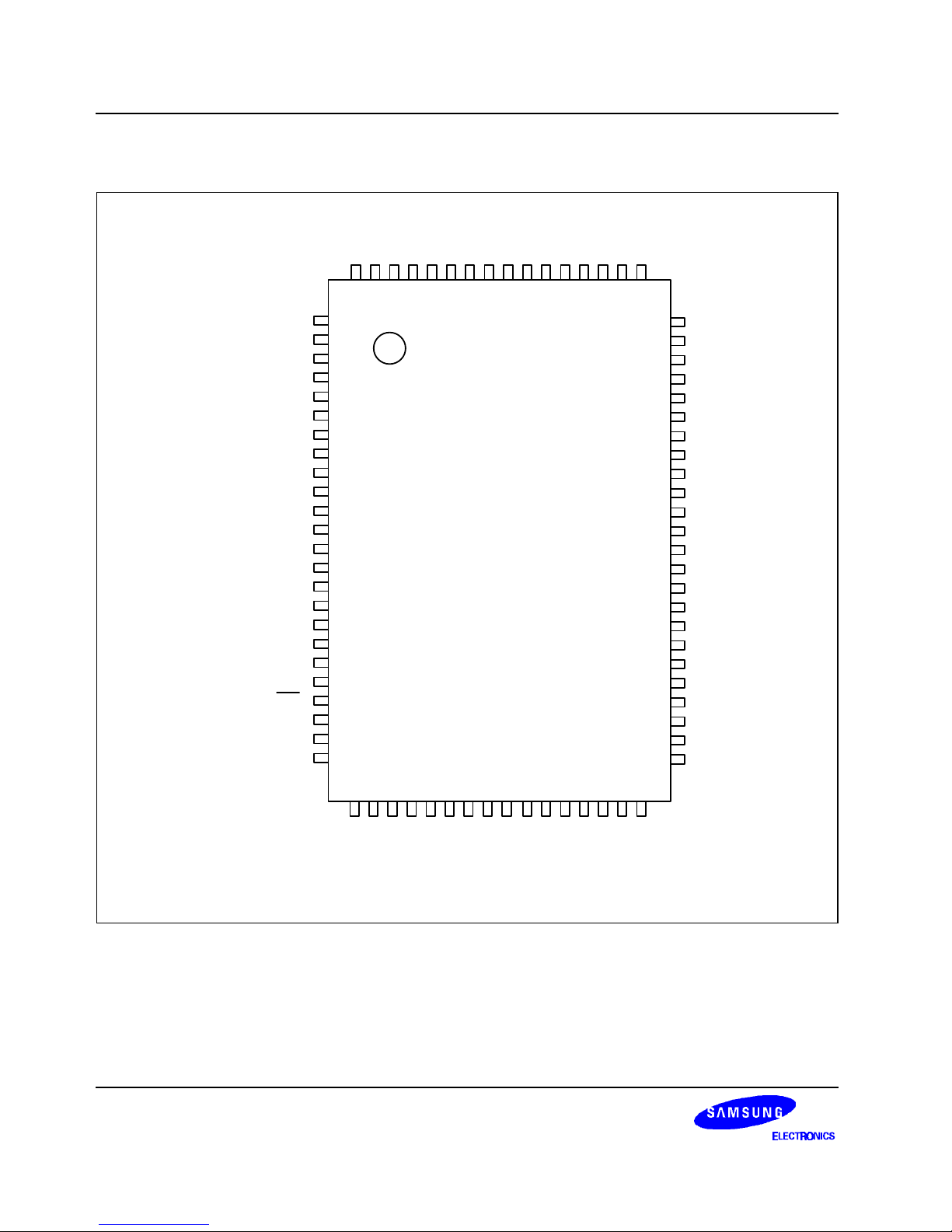
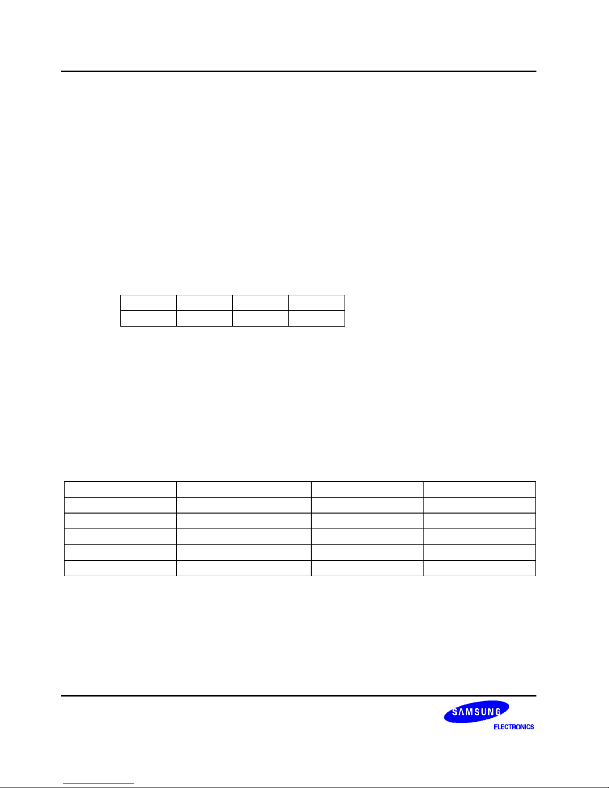
PIN ASSIGNMENTS
SEG19
SEG20
SEG21
SEG22
SEG23
P8.0/SEG24
P8.1/SEG25
P8.2/SEG26
P8.3/SEG27
P8.4/SEG28
P8.5/SEG29
P8.6/SEG30
P8.7/SEG31
P7.3/KS7
P7.2/KS6
P7.1/KS5
P7.0/KS4
P6.3/KS3
P6.2/KS2
P6.1/KS1
P6.0/KS0
P5.3
P5.2
P5.1
64
63
62
61
60
59
58
57
56
55
54
53
52
51
50
49
48
47
46
45
44
43
42
41
80
79
78
77
76
75
74
73
72
71
70
69
68
67
66
65
1
2
3
4
5
6
7
8
9
10
11
12
13
14
15
16
17
18
19
20
21
22
23
24
25
26
27
28
29
30
31
32
33
34
35
36
37
38 3940
KS57C2308
KS57C2316
(TOP VIEW)
SEG2
SEG1
SEG0
COM0
COM1
COM2
COM3
BIAS
VLC0
VLC1
VLC2
VDD
VSS
X
OUT
XIN
TEST
XTIN
XT
OUT
RESET
P0.0/INT4
P0.1/SCK
P0.2/SO
P0.3/SI
P1.0/INT0
P1.1/INT1
P1.2/INT2
P1.3/TCL0
P2.0/TCLO0
P2.1
P2.2/CLO
P2.3/BUZ
P3.0/LCDCK
P3.1/SCDSY
P3.2
P3.3
P4.0
P4.1
P4.2
P4.3
P5.0
SEG3
SEG4
SEG5
SEG6
SEG7
SEG8
SEG9
SEG10
SEG11
SEG12
SEG13
SEG14
SEG15
SEG16
SEG17
SEG18
Figure 1-2. KS57C2308/C2316 80-QFP Pin Assignment Diagram
KS57C2308/P2308/C2316/P2316 PRODUCT OVERVIEW
1-5
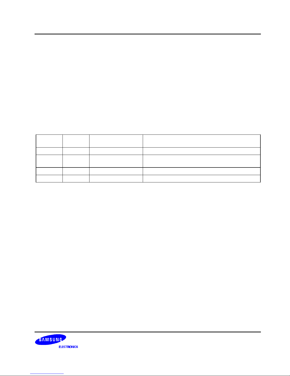
PIN DESCRIPTIONS
Table 1-1. KS57C2308/C2316 Pin Descriptions
Pin Name Pin
Type
Description Number Share
Pin
Reset
Value
Circuit
Type
P0.0
P0.1
P0.2
P0.3
I
I/O
I/O
I
4-bit input port.
1-bit and 4-bit read and test are possible.
4-bit pull-up resistors are software assignable.
20
21
22
23
INT4
SCK
SO
SI
Input A-1
D
*
D
*
A-1
P1.0
P1.1
P1.2
P1.3
I 4-bit input port.
1-bit and 4-bit read and test are possible.
4-bit pull-up resistors are software assignable.
24
25
26
27
INT0
INT1
INT2
TCL0
Input A-1
P2.0
P2.1
P2.2
P2.3
I/O 4-bit I/O port.
1-bit and 4-bit read/write and test are possible.
4-bit pull-up resistors are software assignable.
28
29
30
31
TCLO0
–
CLO
BUZ
Input D
P3.0
P3.1
P3.2
P3.3
I/O 4-bit I/O port.
1-bit and 4-bit read/write and test are possible.
Each individual pin can be specified as input
or output. 4-bit pull-up resistors are software
assignable.
32
33
34
35
LCDCK
LCDSY
Input D
P4.0–
P4.3
P5.0–
P5.3
I/O 4-bit I/O ports. N-channel open-drain output up
to 5 V. 1-, 4-, and 8-bit read/write and test are
possible. Ports 4 and 5 can be paired to
support 8-bit data transfer. 4-bit pull-up
resistors are software assignable.
36–43 – Input E
P6.0–
P6.3
P7.0–
P7.3
I/O 4-bit I/O ports. Port 6 pins are individually
software configurable as input or output. 1-bit
and 4-bit read/write and test are possible. 4-bit
pull-up resistors are software assignable. Ports
6 and 7 can be paired to enable 8-bit data
transfer.
44–51 KS0–KS3
KS4–KS7
Input
D
*
P8.0–
P8.7
O Output port for 1-bit data (for use as CMOS
driver only)
59–52 SEG24–
SEG31
Output H-16
SEG0–
SEG23
O LCD segment signal output 3–1,
80–60
– Output H-15
SEG24–
SEG31
O LCD segment signal output 59–52 P8.0–P8.7 Output H-16
COM0–
COM3
O LCD common signal output 4–7 – Output H-15
V
LC0–VLC2
– LCD power supply. Voltage dividing resistors
are assignable by mask option
9–11 SCLK
SDAT
– –
BIAS – LCD power control 8 – – –
LCDCK I/O LCD clock output for display expansion 32 P3.0 Input D
PRODUCT OVERVIEW KS57C2308/P2308/C2316/P2316
1-6
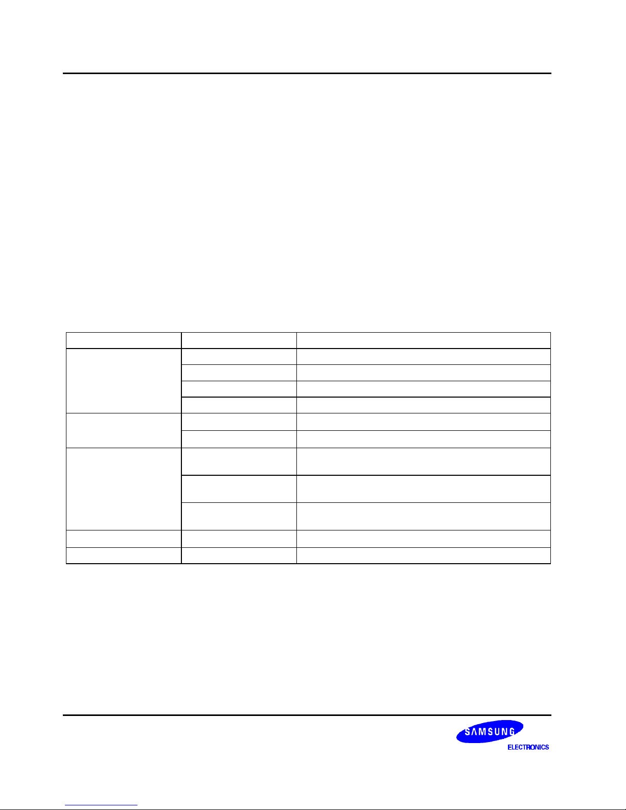
Table 1-1. KS57C2308/C2316 Pin Descriptions (Continued)
Pin Name Pin
Type
Description Number Share
Pin
Reset
Value
Circuit
Type
LCDSY I/O LCD synchronization clock output for LCD
display expansion
33 P3.1 Input D
TCL0 I/O External clock input for timer/counter 0 27 P1.3 Input A-1
TCLO0 I/O Timer/counter 0 clock output 28 P2.0 Input D
SI I Serial interface data input 23 P0.3 Input A-1
SO I/O Serial interface data output 22 P0.2 Input
D
*
SCK
I/O Serial I/O interface clock signal 21 P0.1 Input
D
*
INT0
INT1
I External interrupts. The triggering edge for
INT0 and INT1 is selectable. Only INT0 is
synchronized with the system clock.
24
25
P1.0
P1.1
Input A-1
INT2 I Quasi-interrupt with detection of rising edge
signals.
26 P1.2 Input A-1
INT4 I External interrupt input with detection of rising
or falling edge
20 P0.0 Input A-1
KS0–KS7 I/O Quasi-interrupt inputs with falling edge
detection.
44–51 P6.0–P7.3 Input
D
*
CLO I/O CPU clock output 30 P2.2 Input D
BUZ I/O 2, 4, 8 or 16 kHz frequency output for buzzer
sound with 4.19 MHz main system clock or
32.768 kHz subsystem clock.
31 P2.3 Input D
X
IN,
X
OUT
– Crystal, ceramic or RC oscillator pins for main
system clock. (For external clock input, use
XIN and input XIN‘s reverse phase to X
OUT
)
15,14 – – –
XT
IN,
XT
OUT
– Crystal oscillator pins for subsystem clock.
(For external clock input, use XTIN and input
XTIN's reverse phase to XT
OUT
)
17,18 – – –
V
DD
– Main power supply 12 – – –
V
SS
– Ground 13 – – –
RESET
– Reset signal 19 – Input B
TEST –
Test signal input (must be connected to VSS)
16 – – –
NOTES:
1. Pull-up resistors for all I/O ports are automatically disabled if they are configured to output mode.
2. D * Type has a schmitt trigger circuit at input.
KS57C2308/P2308/C2316/P2316 PRODUCT OVERVIEW
1-7
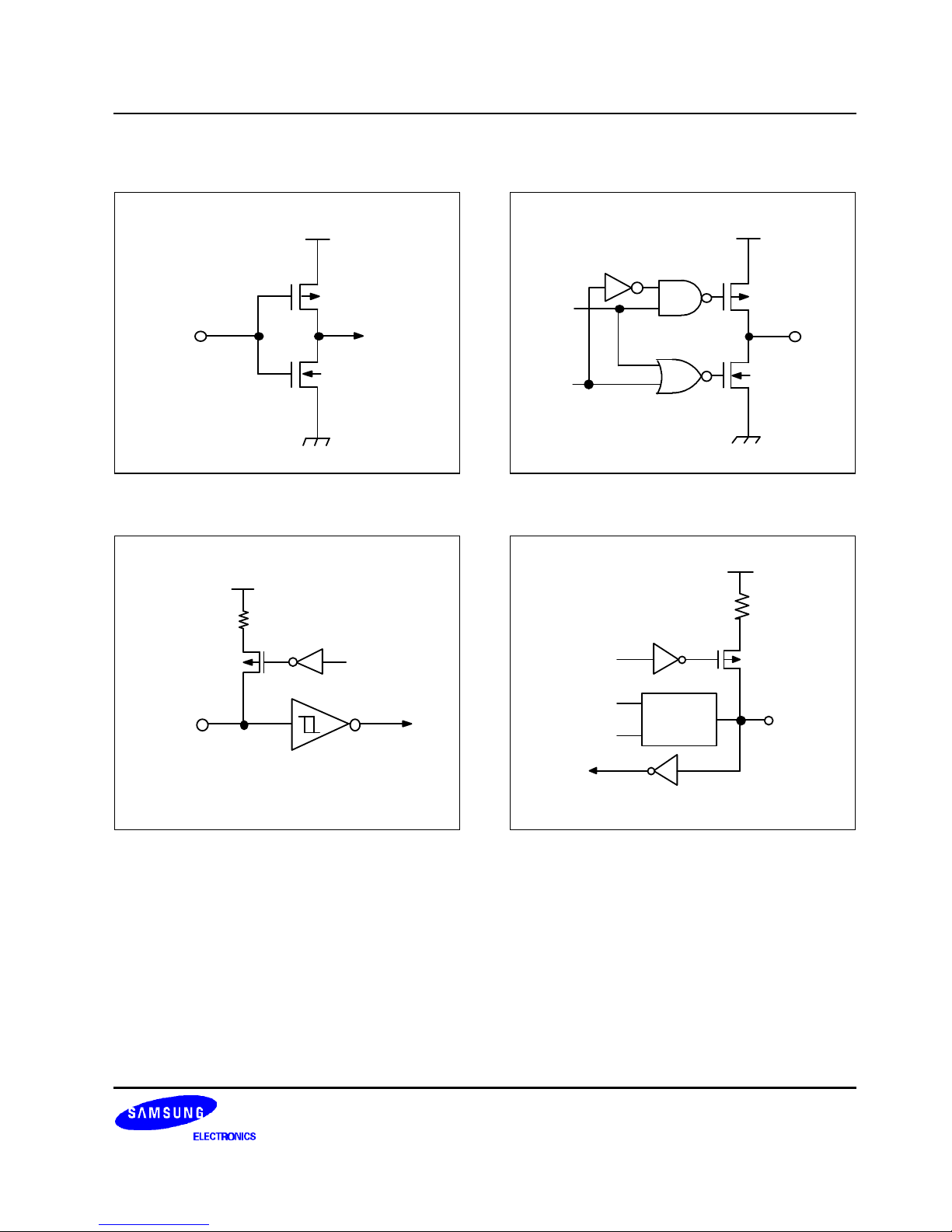
PIN CIRCUIT DIAGRAMS
V
DD
P-CHANNEL
IN
N-CHNNEL
Figure 1-3. Pin Circuit Type A
SCHMITT TRIGGER
V
DD
IN
P-CHANNEL
PULL-UP
RESISTOR
RESISTOR
ENABLE
Figure 1-4. Pin Circuit Type A-1 (P1, P0.0, P0.3)
V
DD
P-CHANNEL
DATA
OUTPUT
DISABLE
N-CHANNEL
OUT
Figure 1-5. Pin Circuit Type C
P-CHANNEL
PULL-UP
RESISTOR
RESISTOR
ENABLE
DATA
OUTPUT
DISABLE
CIRCUIT TYPE A
I/O
V
DD
CIRCUIT
TYPE C
Figure 1-6. Pin Circuit Type D
(P0.1, P0.2, P2, P3, P6, P7)
PRODUCT OVERVIEW KS57C2308/P2308/C2316/P2316
1-8
DATA
OUTPUT
ENABLE
V
DD
P-CH
RESISTOR
ENABLE
N-CH
PULL-UP
RESISTOR
I/O
CIRCUIT TYPE A
V
DD
PNE
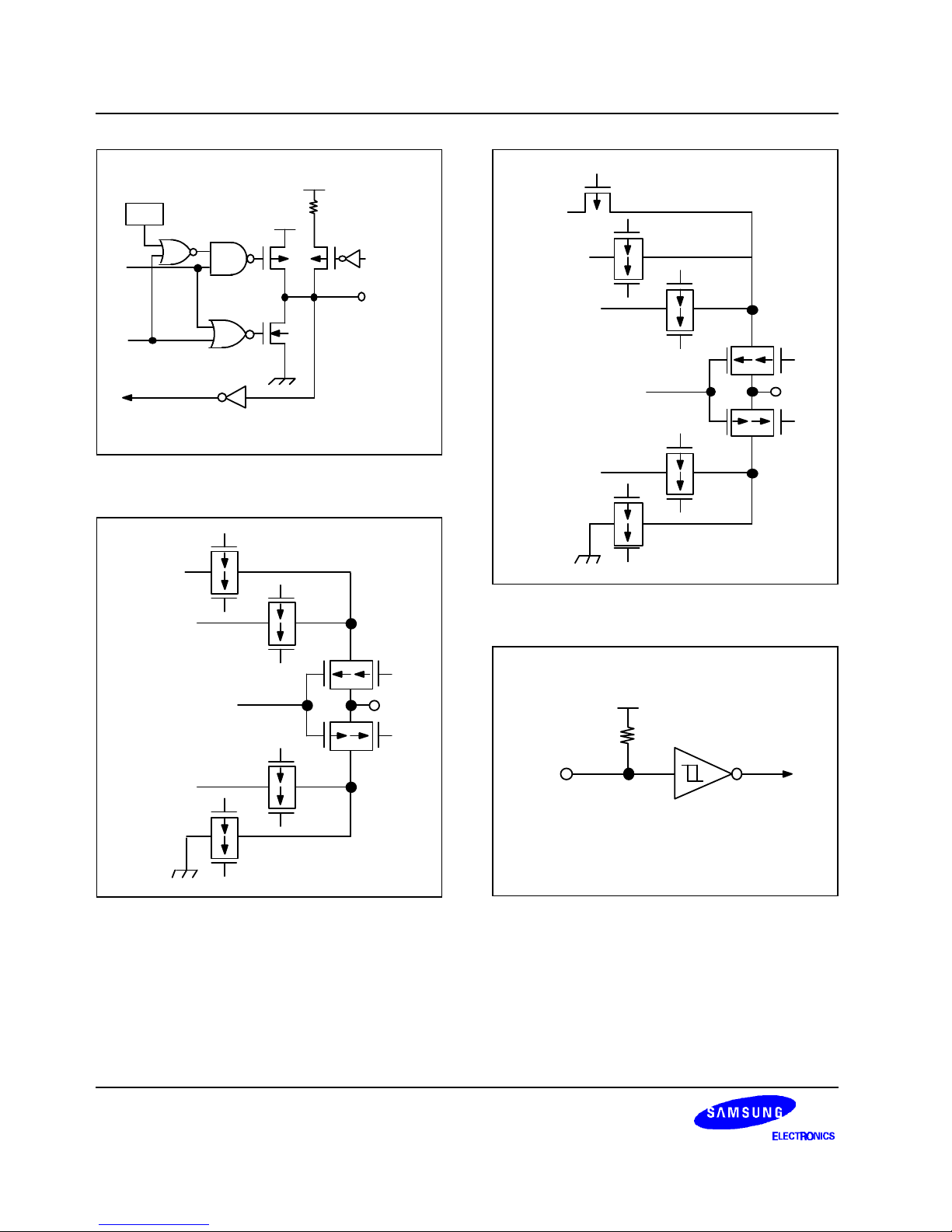
Figure 1-7. Pin Circuit Type E (P4, P5)
V
LC0
V
LC1
LCD SEGMENT/
COMMON DATA
V
LC2
OUT
Figure 1-8. Pin Circuit Type H-15 (SEG/COM)
V
LC0
V
LC1
LCD SEGMENT/
& PORT 8 DATA
V
LC2
V
DD
OUT
Figure 1-9. Pin Circuit Type H-16 (P8)
IN
SCHMITT TRIGGER
V
DD
Figure 1-10. Pin Circuit Type B (RESET)
KS57C2308/P2308/C2316/P2316 ADDRESS SPACES
2-1
2 ADDRESS SPACES
PROGRAM MEMORY (ROM)
OVERVIEW
ROM maps for KS57C2 308/C2316 devices are mask programmable at the factory. KS57C2308 has 8K × 8-bit
program memory and KS57C2316 has 16K × 8-bit program memory, aside from the differences in the ROM size
the two products are identical in other features. In its standard configuration, the device's 8,192 × 8-bit (16,384 ×
8-bit) program memory has four areas that are directly addressable by the program counter (PC):
— 12-byte area for vector addresses
— 96-byte instruction reference area
— 20-byte general-purpose area
— 8064-byte general-purpose area (KS57C2308)
— 16256-byte general-purpose area (KS57C2316)
General-Purpose Program Memory
Two program memory areas are allocated for general-purpose use: One area is 20 bytes in size and the other is
8,064-bytes (16,256-bytes).
Vector Addresses
A 12-byte vector address area is used to store the vector addresses required to execute system resets and
interrupts. Start addresses for interrupt service routines are stored in this area, along with the values of the
enable memory bank (EMB) and enable register bank (ERB) flags that are used to set their initial value for the
corresponding service routines. The 16-byte area can be used alternately as general-purpose ROM.
REF Instructions
Locations 0020H–007FH are used as a reference area (look-up table) for 1-byte REF instructions. The REF
instruction reduces the byte size of instruction operands. REF can reference one 2-byte instruction, two 1-byte
instructions, and one 3-byte instruction which are stored in the look-up table. Unused look-up table addresses can
be used as general-purpose ROM.
Table 2-1. Program Memory Address Ranges
ROM Area Function Address Ranges Area Size (in Bytes)
Vector address area 0000H–000BH 12
General-purpose program memory 000CH–001FH 20
REF instruction look-up table area 0020H–007FH 96
General-purpose program memory 0080H–1FFFH (KS57C2308)
0080H–3FFFH (KS57C2316)
8064 (KS57C2308)
16256 (KS57C2316)
ADDRESS SPACES KS57C2308/P2308/C2316/P2316
2-2
GENERAL-PURPOSE MEMORY AREAS
The 20-byte area at ROM locations 000CH–001FH and the 8,064-byte (16,256-byte) area at ROM locations
0080H–1FFFH (0080H–3FFFH) are used as general-purpose program memory. Unused locations in the vector
address area and REF instruction look-up table areas can be used as general-purpose program memory.
However, care must be taken not to overwrite live data when writing programs that use special-purpose areas of
the ROM.
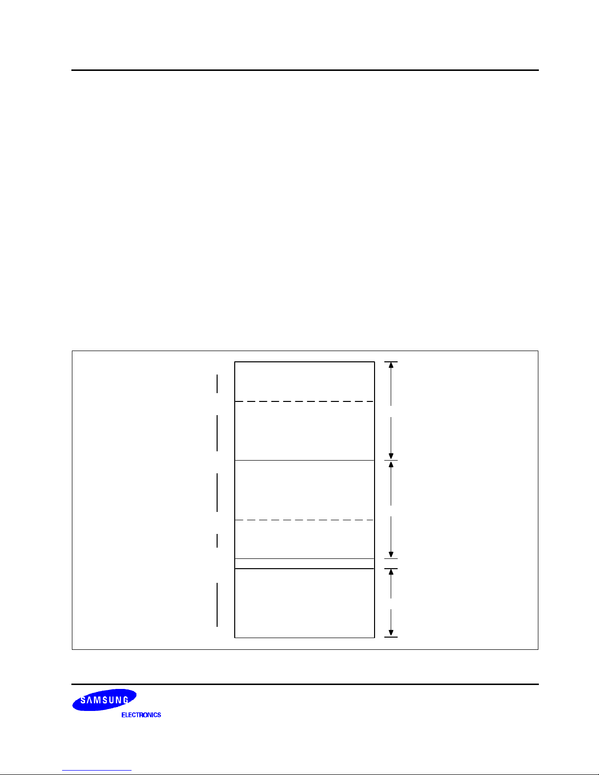
VECTOR ADDRESS AREA
The 12-byte vector address area of the ROM is used to store the vector addresses for executing system resets
and interrupts. The starting addresses of interrupt service routines are stored in this area, along with the enable
memory bank (EMB) and enable register bank (ERB) flag values that are needed to initialize the service routines.
12-byte vector addresses are organized as follows:
NOTE: PC13 is used for KS57C2316/P2316 microcontroller.
To set up the vector address area for specific programs, use the instruction VENTn. The programming tips on the
next page explain how to do this.
VECTOR ADDRESS AREA
(12 Bytes)
GENERAL-PURPOSE AREA
(20 Bytes)
INSTRUCTION
REFERENCE
AREA
GENERAL-PURPOSE AREA
(8,064 Bytes/
16,256 Bytes)
1FFFH
3FFFH
0080H
007FH
0020H
001FH
000CH
000BH
0000H
Figure 2-1. ROM Address Structure
7 6 5 4 3 2 1 0
RESET
INTB/INT4
INT0
INT1
INTT0
0000H
0002H
0004H
0006H
0008H
000AH
INTS
Figure 2-2. Vector Address Structure
EMB ERB
PC13
(note)
PC12 PC11 PC10 PC9 PC8
PC7 PC6 PC5 PC4 PC3 PC2 PC1 PC0

KS57C2308/P2308/C2316/P2316 ADDRESS SPACES
2-3
++ PROGRAMMING TIP — Defining Vectored Interrupts
The following examples show you several ways you can define the vectored interrupt and instruction reference
areas in program memory:
1. When all vector interrupts are used:
ORG 0000H
VENT0 1,0,RESET ; EMB ← 1, ERB ← 0; Jump to RESET address by RESET
VENT1 0,0,INTB ; EMB ← 0, ERB ← 0; Jump to INTB address by INTB
VENT2 0,0,INT0 ; EMB ← 0, ERB ← 0; Jump to INT0 address by INT0
VENT3 0,0,INT1 ; EMB ← 0, ERB ← 0; Jump to INT1 address by INT1
VENT4 0,0,INTS ; EMB ← 0, ERB ← 0; Jump to INTS address by INTS
VENT5 0,0,INTT0 ; EMB ← 0, ERB ← 0; Jump to INTT0 address by INTT0
2. When a specific vectored interrupt such as INT0, and INTT0 is not used, the unused vector interrupt
locations must be skipped with the assembly instruction ORG so that jumps will address the correct locations:
ORG 0000H
VENT0 1,0,RESET ; EMB ← 1, ERB ← 0; Jump to RESET address by RESET
VENT1 0,0,INTB ; EMB ← 0, ERB ← 0; Jump to INTB address by INTB
ORG 0006H ; INT0 interrupt not used
VENT3 0,0,INT1 ; EMB ← 0, ERB ← 0; Jump to INT1 address by INT1
VENT4 0,0,INTS ; EMB ← 0, ERB ← 0; Jump to INTS address by INTS
ORG 000CH ; INTT0 interrupt not used
ORG 0010H
3. If an INT0 interrupt is not used and if its corresponding vector interrupt area is not fully utilized, or if it is not
written by a ORG instruction in Example 2, a CPU malfunction will occur:
ORG 0000H
VENT0 1,0,RESET ; EMB ← 1, ERB ← 0; Jump to RESET address by RESET
VENT1 0,0,INTB ; EMB ← 0, ERB ← 0; Jump to INTB address by INTB
VENT3 0,0,INT1 ; EMB ← 0, ERB ← 0; Jump to INT1 address by INT0
VENT4 0,0,INTS ; EMB ← 0, ERB ← 0; Jump to INTS address by INT1
VENT5 0,0,INTT0 ; EMB ← 0, ERB ← 0; Jump to INTT0 address by INTS
ORG 0010H
General-purpose ROM area
In this example, when an INTS interrupt is generated, the corresponding vector area is not VENT4 INTS, but
VENT5 INTT0. This causes an INTS interrupt to jump incorrectly to the INTT0 address and causes a CPU
malfunction to occur.

ADDRESS SPACES KS57C2308/P2308/C2316/P2316
2-4
INSTRUCTION REFERENCE AREA
Using 1-byte REF instructions, you can easily reference instructions with larger byte sizes that are stored in
addresses 0020H–007FH of program memory. This 96-byte area is called the REF instruction reference area, or
look-up table. Locations in the REF look-up table may contain two 1-byte instructions, one 2-byte instruction, or
one 3-byte instruction such as a JP (jump) or CALL. The starting address of the instruction you are referencing
must always be an even number. To reference a JP or CALL instruction, it must be written to the reference area
in a two-byte format: for JP, this format is TJP; for CALL, it is TCALL.
By using REF instructions you can execute instructions larger than one byte, In summary, there are three ways
you can use the REF instruction:
— Using the 1-byte REF instruction to execute one 2-byte or two 1-byte instructions,
— Branching to any location by referencing a branch instruction stored in the look-up table,
— Calling subroutines at any location by referencing a call instruction stored in the look-up table.
++ PROGRAMMING TIP — Using the REF Look-Up Table
Here is one example of how to use the REF instruction look-up table:
ORG 0020H
JMAIN TJP MAIN ; 0, MAIN
KEYCK BTSF KEYFG ; 1, KEYFG CHECK
WATCH TCALL CLOCK ; 2, CALL CLOCK
INCHL LD @HL,A ; 3, (HL) ← A
INCS HL
•
•
•
ABC LD EA,#00H ; 47, EA ← #00H
ORG 0080H
MAIN NOP
NOP
•
•
•
REF KEYCK ; BTSF KEYFG (1-byte instruction)
REF JMAIN ; KEYFG = 1, jump to MAIN (1-byte instruction)
REF WATCH ; KEYFG = 0, CALL CLOCK (1-byte instruction)
REF INCHL ; LD @HL,A
; INCS HL
REF ABC ; LD EA,#00H (1-byte instruction)
•
•
•
KS57C2308/P2308/C2316/P2316 ADDRESS SPACES
2-5
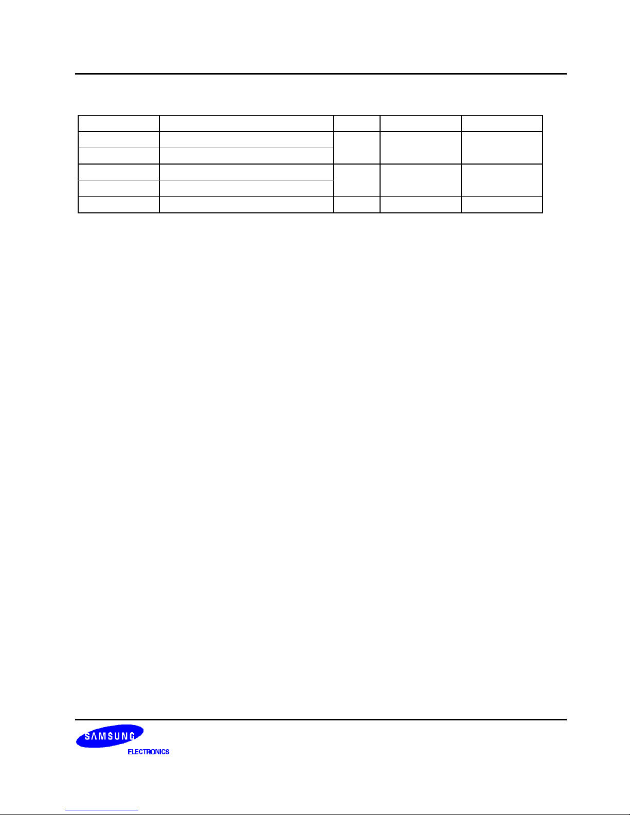
DATA MEMORY (RAM)
OVERVIEW
In its standard configuration, the 512 x 4-bit data memory has four areas:
— 32 × 4-bit working register area in bank 0
— 224 × 4-bit general-purpose area in bank 0 which is also used as the stack area
— 224 × 4-bit general-purpose area in bank 1
— 32 × 4-bit area for LCD data in bank 1
— 128 × 4-bit area in bank 15 for memory-mapped I/O addresses
To make it easier to reference, the data memory area has three memory banks — bank 0, bank 1 and bank 15.
The select memory bank instruction (SMB) is used to select the bank you want to select as working data memory.
Data stored in RAM locations are 1-, 4-, and 8-bit addressable. One exception is the LCD data register area,
which is 1-bit and 4-bit addressable only.
Initialization values for the data memory area are not defined by hardware and must therefore be initialized by
program software following power RESET. However, when RESET signal is generated in power-down mode, the
most of data memory contents are held.
GENERAL-PURPOSE
REGISTERS AND
STACK AREA
(224 x 4 Bits)
WORKING REGISTERS
(32 x 4 Bits)
LCD DATA REGISTERS
(32 x 4 Bits)
MEMORY-MAPPED I/O
AEERESS REGISTERS
(128 x 4 Bits)
000H
01FH
020H
0FFH
100H
FFFH
1FFH
F80H
~~
BANK 0
BANK 1
BANK 15
GENERAL-PURPOSE
REGISTERS
(224 x 4 Bits)
1DFH
1E0H
Figure 2-3. Data Memory (RAM) Map

ADDRESS SPACES KS57C2308/P2308/C2316/P2316
2-6
Memory Banks 0, 1, and 15
Bank 0 (000H–0FFH) The lowest 32 nibbles of bank 0 (000H–01FH) are used as working registers;
the next 224 nibbles (020H–0FFH) can be used both as stack area and as
general-purpose data memory. Use the stack area for implementing subroutine
calls and returns, and for interrupt processing.
Bank 1 (100H–1FFH) The lowest 224 nibbles of bank1 (100H–1DFH) are for general–purpose use;
Use the remaining of 32 nibbles (1E0H–1FFH) as display registers or as
general purpose memory.
Bank 15 (F80H–FFFH) The microcontroller uses bank 15 for memory-mapped peripheral I/O. Fixed
RAM locations for each peripheral hardware address are mapped into this
area.
Data Memory Addressing Modes
The enable memory bank (EMB) flag controls the addressing mode for data memory banks 0, 1 or 15. When the
EMB flag is logic zero, the addressable area is restricted to specific locations, depending on whether direct or
indirect addressing is used. With direct addressing, you can access locations 000H–07FH of bank 0 and bank 15.
With indirect addressing, only bank 0 (000H–0FFH) can be accessed. When the EMB flag is set to logic one, all
three data memory banks can be accessed according to the current SMB value.
For 8-bit addressing, two 4-bit registers are addressed as a register pair. Also, when using 8-bit instructions to
address RAM locations, remember to use the even-numbered register address as the instruction operand.
Working Registers
The RAM working register area in data memory bank 0 is further divided into four register banks (bank 0, 1, 2,
and 3). Each register bank has eight 4-bit registers and paired 4-bit registers are 8-bit addressable.
Register A is used as a 4-bit accumulator and register pair EA as an 8-bit extended accumulator. The carry flag
bit can also be used as a 1-bit accumulator. Register pairs WX, WL, and HL are used as address pointers for
indirect addressing. To limit the possibility of data corruption due to incorrect register addressing, it is advisable
to use register bank 0 for the main program and banks 1, 2, and 3 for interrupt service routines.
LCD Data Register Area
Bit values for LCD segment data are stored in data memory bank 1. Register locations in this area that are not
used to store LCD data can be assigned to general-purpose use.
KS57C2308/P2308/C2316/P2316 ADDRESS SPACES
2-7
Table 2-2. Data Memory Organization and Addressing
Addresses Register Areas Bank EMB Value SMB Value
000H–01FH Working registers 0 0, 1 0
020H–0FFH Stack and general-purpose registers
100H–1DFH General-purpose registers 1 1 1
1E0H–1FFH LCD Data registers
F80H–FFFH I/O-mapped hardware registers 15 0, 1 15
++ PROGRAMMING TIP — Clearing Data Memory Banks 0 and 1
Clear banks 0 and 1 of the data memory area:
RAMCLR SMB 1 ; RAM (100H–1FFH) clear
LD HL,#00H
LD A,#0H
RMCL1 LD @HL,A
INCS HL
JR RMCL1
SMB 0 ; RAM (010H–0FFH) clear
LD HL,#10H
RMCL0 LD @HL,A
INCS HL
JR RMCL0
ADDRESS SPACES KS57C2308/P2308/C2316/P2316
2-8
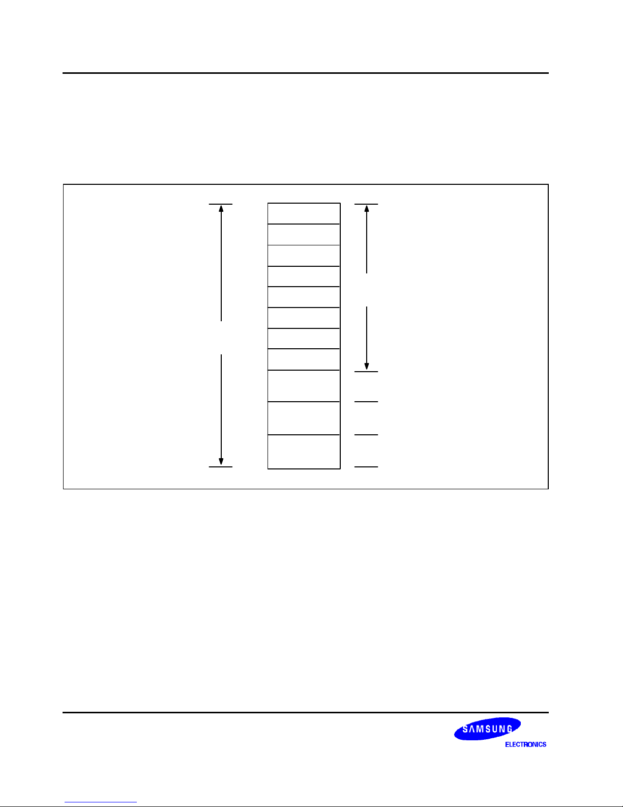
WORKING REGISTERS
Working registers, mapped to RAM address 000H-01FH in data memory bank 0, are used to temporarily store
intermediate results during program execution, as well as pointer values used for indirect addressing. Unused
registers may be used as general-purpose memory. Working register data can be manipulated as 1-bit units, 4-bit
units or, using paired registers, as 8-bit units.
000H
001H
002H
003H
004H
005H
006H
007H
00FH
010H
017H
018H
01FH
008H
A
E
L
H
X
W
Z
Y
A
...
Y
REGISTER
BANK 1
REGISTER
BANK 2
REGISTER
BANK 3
A
...
Y
A
...
Y
WORKING
REGISTER
BANK 0
DATA
MEMORY
BANK 0
Figure 2-4. Working Register Map
KS57C2308/P2308/C2316/P2316 ADDRESS SPACES
2-9
Working Register Banks
For addressing purposes, the working register area is divided into four register banks — bank 0, bank 1, bank 2,
and bank 3. Any one of these banks can be selected as the working register bank by the register bank selection
instruction (SRB n) and by setting the status of the register bank enable flag (ERB).
Generally, working register bank 0 is used for the main program, and banks 1, 2, and 3 for interrupt service
routines. Following this convention helps to prevent possible data corruption during program execution due to
contention in register bank addressing.
Table 2-3. Working Register Organization and Addressing
ERB Setting SRB Settings Selected Register Bank
3 2 1 0
0 0 0 – – Always set to bank 0
0 0 Bank 0
1 0 0 0 1 Bank 1
1 0 Bank 2
1 1 Bank 3
Paired Working Registers
Each of the register banks is subdivided into eight 4-bit registers. These registers, named Y, Z, W, X, H, L, E and
A, can either be manipulated individually using 4-bit instructions, or together as register pairs for 8-bit data
manipulation.
The names of the 8-bit register pairs in each register bank are EA, HL, WX, YZ and WL. Registers A, L, X and Z
always become the lower nibble when registers are addressed as 8-bit pairs. This makes a total of eight 4-bit
registers or four 8-bit double registers in each of the four working register banks.
Y Z
W X
H L
E A
(MSB)
(LSB) (MSB) (LSB)
Figure 2-5. Register Pair Configuration
ADDRESS SPACES KS57C2308/P2308/C2316/P2316
2-10
Special-Purpose Working Registers
Register A is used as a 4-bit accumulator and double register EA as an 8-bit accumulator. The carry flag can also
be used as a 1-bit accumulator.
8-bit double registers WX, WL and HL are used as data pointers for indirect addressing. When the HL register
serves as a data pointer, the instructions LDI, LDD, XCHI, and XCHD can make very efficient use of working
registers as program loop counters by letting you transfer a value to the L register and increment or decrement it
using a single instruction.
C
A
EA
1-BIT
ACCUMULATOR
4-BIT
ACCUMULATOR
8-BIT
ACCUMULATOR
Figure 2-6. 1-Bit, 4-Bit, and 8-Bit Accumulator
Recommendation for Multiple Interrupt Processing
If more than four interrupts are being processed at one time, you can avoid possible loss of working register data
by using the PUSH RR instruction to save register contents to the stack before the service routines are executed
in the same register bank. When the routines have executed successfully, you can restore the register contents
from the stack to working memory using the POP instruction.

KS57C2308/P2308/C2316/P2316 ADDRESS SPACES
2-11
++ PROGRAMMING TIP — Selecting the Working Register Area
The following examples show the correct programming method for selecting working register area:
1. When ERB = "0":
VENT2 1,0,INT0 ; EMB ← 1, ERB ← 0, Jump to INT0 address
INT0 PUSH SB ; PUSH current SMB, SRB
SRB 2 ; Instruction does not execute because ERB = "0"
PUSH HL ; PUSH HL register contents to stack
PUSH WX ; PUSH WX register contents to stack
PUSH YZ ; PUSH YZ register contents to stack
PUSH EA ; PUSH EA register contents to stack
SMB 0
LD EA,#00H
LD 80H,EA
LD HL,#40H
INCS HL
LD WX,EA
LD YZ,EA
POP EA ; POP EA register contents from stack
POP YZ ; POP YZ register contents from stack
POP WX ; POP WX register contents from stack
POP HL ; POP HL register contents from stack
POP SB ; POP current SMB, SRB
IRET
The POP instructions execute alternately with the PUSH instructions. If an SMB n instruction is used in an
interrupt service routine, a PUSH and POP SB instruction must be used to store and restore the current SMB and
SRB values, as shown in Example 2 below.
2. When ERB = "1":
VENT2 1,1,INT0 ; EMB ← 1, ERB ← 1, Jump to INT0 address
INT0 PUSH SB ; Store current SMB, SRB
SRB 2 ; Select register bank 2 because of ERB = "1"
SMB 0
LD EA,#00H
LD 80H,EA
LD HL,#40H
INCS HL
LD WX,EA
LD YZ,EA
POP SB ; Restore SMB, SRB
IRET
ADDRESS SPACES KS57C2308/P2308/C2316/P2316
2-12
STACK OPERATIONS
STACK POINTER (SP)
The stack pointer (SP) is an 8-bit register that stores the address used to access the stack, an area of data
memory set aside for temporary storage of data and addresses. The SP can be read or written by 8-bit control
instructions. When addressing the SP, bit 0 must always remain cleared to logic zero.
F80H SP3 SP2 SP1 "0"
F81H SP7 SP6 SP5 SP4
There are two basic stack operations: writing to the top of the stack (push), and reading from the top of the stack
(pop). A push decrements the SP and a pop increments it so that the SP always points to the top address of the
last data to be written to the stack.
The program counter contents and program status word are stored in the stack area prior to the execution of a
CALL or a PUSH instruction, or during interrupt service routines. Stack operation is a LIFO (Last In-First Out)
type. The stack area is located in general-purpose data memory bank 0.
During an interrupt or a subroutine, the PC value and the PSW are saved to the stack area. When the routine has
completed, the stack pointer is referenced to restore the PC and PSW, and the next instruction is executed.
The SP can address stack registers in bank 0 (addresses 000H-0FFH) regardless of the current value of the
enable memory bank (EMB) flag and the select memory bank (SMB) flag. Although general-purpose register
areas can be used for stack operations, be careful to avoid data loss due to simultaneous use of the same
register(s).
Since the RESET value of the stack pointer is not defined in firmware, we recommend that you initialize the stack
pointer by program code to location 00H. This sets the first register of the stack area to 0FFH.
NOTE
A subroutine call occupies six nibbles in the stack; an interrupt requires six. When subroutine nesting or
interrupt routines are used continuously, the stack area should be set in accordance with the maximum
number of subroutine levels. To do this, estimate the number of nibbles that will be used for the
subroutines or interrupts and set the stack area correspondingly.
++ PROGRAMMING TIP — Initializing the Stack Pointer
To initialize the stack pointer (SP):
1. When EMB = "1":
SMB 15 ; Select memory bank 15
LD EA,#00H ; Bit 0 of SP is always cleared to "0"
LD SP,EA ; Stack area initial address (0FFH) ← (SP) – 1
2. When EMB = "0":
LD EA,#00H
LD SP,EA ; Memory addressing area (00H–7FH, F80H–FFFH)
KS57C2308/P2308/C2316/P2316 ADDRESS SPACES
2-13
PUSH OPERATIONS
Three kinds of push operations reference the stack pointer (SP) to write data from the source register to the
stack: PUSH instructions, CALL instructions, and interrupts. In each case, the SP is decreased by a number
determined by the type of push operation and then points to the next available stack location.
PUSH Instructions
A PUSH instruction references the SP to write two 4-bit data nibbles to the stack. Two 4-bit stack addresses are
referenced by the stack pointer: one for the upper register value and another for the lower register. After the
PUSH has executed, the SP is decreased by two and points to the next available stack location.
CALL Instructions
When a subroutine call is issued, the CALL instruction references the SP to write the PC's contents to six 4-bit
stack locations. Current values for the enable memory bank (EMB) flag and the enable register bank (ERB) flag
are also pushed to the stack. Since six 4-bit stack locations are used per CALL, you may nest subroutine calls up
to the number of levels permitted in the stack.
Interrupt Routines
An interrupt routine references the SP to push the contents of the PC and the program status word (PSW) to the
stack. Six 4-bit stack locations are used to store this data. After the interrupt has executed, the SP is decreased
by six and points to the next available stack location. During an interrupt sequence, subroutines may be nested
up to the number of levels which are permitted in the stack area.
SP - 2
SP - 1
SP
LOWER
UPPER
PUSH
(After PUSH, SP SP - 2)
SP - 6
SP - 5
SP - 4
SP - 3
SP - 2
SP - 1
SP
CALL
(After CALL, SP SP - 6)
0 0
PC3 - PC0
PC7 - PC4
0 0 EMB ERB
0 0 0 0
PC11- PC8
INTERRUP
(When INT is acknowledged,
SP SP - 6)
SP - 6
SP - 5
SP - 4
SP - 3
SP - 2
SP - 1
SP
0 0
PC3 - PC0
PC7 - PC4
IS1 IS0 EMB ERB
PSW
C SC2 SC1 SC0
PC11 - PC8
PSW
PC13 PC12 PC13 PC12
NOTE
: PC13 is used for KS57C2316/P2316 microcontroller
Figure 2-7. Push-Type Stack Operations
ADDRESS SPACES KS57C2308/P2308/C2316/P2316
2-14
POP OPERATIONS
For each push operation there is a corresponding pop operation to write data from the stack back to the source
register or registers: for the PUSH instruction it is the POP instruction; for CALL, the instruction RET or SRET; for
interrupts, the instruction IRET. When a pop operation occurs, the SP is incremented by a number determined by
the type of operation and points to the next free stack location.
POP Instructions
A POP instruction references the SP to write data stored in two 4-bit stack locations back to the register pairs and
SB register. The value of the lower 4-bit register is popped first, followed by the value of the upper 4-bit register.
After the POP has executed, the SP is incremented by two and points to the next free stack location.
RET and SRET Instructions
The end of a subroutine call is signaled by the return instruction, RET or SRET. The RET or SRET uses the SP
to reference the six 4-bit stack locations used for the CALL and to write this data back to the PC, the EMB, and
the ERB. After the RET or SRET has executed, the SP is incremented by six and points to the next free stack
location.
IRET Instructions
The end of an interrupt sequence is signaled by the instruction IRET. IRET references the SP to locate the six
4-bit stack addresses used for the interrupt and to write this data back to the PC and the PSW. After the IRET
has executed, the SP is incremented by six and points to the next free stack location.
LOWER
UPPER
POP
SP SP + 2)
RET OR SRET
SP SP + 6)
0 0
PC3 – PC0
PC7 – PC4
0 0 EMB ERB
0 0 0 0
PC11 – PC8
IRET
SP SP + 6)
0 0
PC3 – PC0
PC7 – PC4
IS1 IS0 EMB ERB
PSW
C SC2 SC1 SC0
PC11 – PC8
SP
SP + 1
SP + 2
SP + 3
SP + 4
SP + 5
SP + 6
SP
SP + 1
SP + 2
SP + 3
SP + 4
SP + 5
SP + 6
SP
SP + 1
SP + 2
PSW
PC13 PC12 PC13 PC12
NOTE
: PC13 is used for KS57C2316/P2316 microcontroller
Figure 2-8. Pop-Type Stack Operations
KS57C2308/P2308/C2316/P2316 ADDRESS SPACES
2-15
BIT SEQUENTIAL CARRIER (BSC)
The bit sequential carrier (BSC) is a 16-bit general register that can be manipulated using 1-, 4-, and 8-bit RAM
control instructions. RESET clears all BSC bit values to logic zero.
Using the BSC, you can specify sequential addresses and bit locations using 1-bit indirect addressing
(memb.@L). (Bit addressing is independent of the current EMB value.) In this way, programs can process 16-bit
data by moving the bit location sequentially and then incrementing or decreasing the value of the L register.
BSC data can also be manipulated using direct addressing. For 8-bit manipulations, the 4-bit register names
BSC0 and BSC2 must be specified and the upper and lower 8 bits manipulated separately.
If the values of the L register are 0H at BSC0.@L, the address and bit location assignment is FC0H.0. If the L
register content is FH at BSC0.@L, the address and bit location assignment is FC3H.3.
Table 2-4. BSC Register Organization
Name Address Bit 3 Bit 2 Bit 1 Bit 0
BSC0 FC0H BSC0.3 BSC0.2 BSC0.1 BSC0.0
BSC1 FC1H BSC1.3 BSC1.2 BSC1.1 BSC1.0
BSC2 FC2H BSC2.3 BSC2.2 BSC2.1 BSC2.0
BSC3 FC3H BSC3.3 BSC3.2 BSC3.1 BSC3.0
++ PROGRAMMING TIP — Using the BSC Register to Output 16-Bit Data
To use the bit sequential carrier (BSC) register to output 16-bit data (5937H) to the P3.0 pin:
BITS EMB
SMB 15
LD EA,#37H ;
LD BSC0,EA ; BSC0 ← A, BSC1 ← E
LD EA,#59H ;
LD BSC2,EA ; BSC2 ← A, BSC3 ← E
SMB 0
LD L,#0H ;
AGN LDB C,BSC0.@L ;
LDB P3.0,C ; P3.0 ← C
INCS L
JR AGN
RET
ADDRESS SPACES KS57C2308/P2308/C2316/P2316
2-16
PROGRAM COUNTER (PC)
A 13-bit program counter (PC) stores addresses for instruction fetches during program execution (KS57C2316
microcontroller has 14-bit program counter, PC0–PC13). Whenever a reset operation or an interrupt occurs, bits
PC12 through PC0 (PC13 through PC0 for KS57C2316) are set to the vector address.
Usually, the PC is incremented by the number of bytes of the instruction being fetched. One exception is the
1-byte REF instruction which is used to reference instructions stored in the ROM.
PROGRAM STATUS WORD (PSW)
The program status word (PSW) is an 8-bit word that defines system status and program execution status and
which permits an interrupted process to resume operation after an interrupt request has been serviced. PSW
values are mapped as follows:
(MSB) (LSB)
FB0H IS1 IS0 EMB ERB
FB1H C SC2 SC1 SC0
The PSW can be manipulated by 1-bit or 4-bit read/write and by 8-bit read instructions, depending on the specific
bit or bits being addressed. The PSW can be addressed during program execution regardless of the current value
of the enable memory bank (EMB) flag.
Part or all of the PSW is saved to stack prior to execution of a subroutine call or hardware interrupt. After the
interrupt has been processed, the PSW values are popped from the stack back to the PSW address.
When a RESET is generated, the EMB and ERB values are set according to the RESET vector address, and the
carry flag is left undefined (or the current value is retained). PSW bits IS0, IS1, SC0, SC1, and SC2 are all
cleared to logical zero.
Table 2-5. Program Status Word Bit Descriptions
PSW Bit Identifier Description Bit Addressing Read/Write
IS1, IS0 Interrupt status flags 1, 4 R/W
EMB Enable memory bank flag 1 R/W
ERB Enable register bank flag 1 R/W
C Carry flag 1 R/W
SC2, SC1, SC0 Program skip flags 8 R
KS57C2308/P2308/C2316/P2316 ADDRESS SPACES
2-17
INTERRUPT STATUS FLAGS (IS0, IS1)
PSW bits IS0 and IS1 contain the current interrupt execution status values. You can manipulate IS0 and IS1
flags directly using 1-bit RAM control instructions
By manipulating interrupt status flags in conjunction with the interrupt priority register (IPR), you can process
multiple interrupts by anticipating the next interrupt in an execution sequence. The interrupt priority control circuit
determines the IS0 and IS1 settings in order to control multiple interrupt processing. When both interrupt status
flags are set to "0", all interrupts are allowed. The priority with which interrupts are processed is then determined
by the IPR.
When an interrupt occurs, IS0 and IS1 are pushed to the stack as part of the PSW and are automatically
incremented to the next higher priority level. Then, when the interrupt service routine ends with an IRET
instruction, IS0 and IS1 values are restored to the PSW. Table 2-6 shows the effects of IS0 and IS1 flag settings.
Table 2-6. Interrupt Status Flag Bit Settings
IS1
Value
IS0
Value
Status of Currently
Executing Process
Effect of IS0 and IS1 Settings
on Interrupt Request Control
0 0 0 All interrupt requests are serviced
0 1 1 Only high-priority interrupt(s) as determined in the
interrupt priority register (IPR) are serviced
1 0 2 No more interrupt requests are serviced
1 1 – Not applicable; these bit settings are undefined
Since interrupt status flags can be addressed by write instructions, programs can exert direct control over
interrupt processing status. Before interrupt status flags can be addressed, however, you must first execute a DI
instruction to inhibit additional interrupt routines. When the bit manipulation has been completed, execute an EI
instruction to re-enable interrupt processing.
++ PROGRAMMING TIP — Setting ISx Flags for Interrupt Processing
The following instruction sequence shows how to use the IS0 and IS1 flags to control interrupt processing:
INTB DI ; Disable interrupt
BITR IS1 ; IS1 ← 0
BITS IS0 ; Allow interrupts according to IPR priority level
EI ; Enable interrupt

ADDRESS SPACES KS57C2308/P2308/C2316/P2316
2-18
EMB FLAG (EMB)
The EMB flag is used to allocate specific address locations in the RAM by modifying the upper 4 bits of 12-bit
data memory addresses. In this way, it controls the addressing mode for data memory banks 0, 1 or 15.
When the EMB flag is "0", the data memory address space is restricted to bank 15 and addresses 000H–07FH of
memory bank 0, regardless of the SMB register contents. When the EMB flag is set to "1", the general-purpose
areas of bank 0, 1 and 15 can be accessed by using the appropriate SMB value.
++ PROGRAMMING TIP — Using the EMB Flag to Select Memory Banks
EMB flag settings for memory bank selection:
1. When EMB = "0":
SMB 1 ; Non-essential instruction since EMB = "0"
LD A,#9H
LD 90H,A ; (F90H) ← A, bank 15 is selected
LD 34H,A ; (034H) ← A, bank 0 is selected
SMB 0 ; Non-essential instruction since EMB = "0"
LD 90H,A ; (F90H) ← A, bank 15 is selected
LD 34H,A ; (034H) ← A, bank 0 is selected
SMB 15 ; Non-essential instruction, since EMB = "0"
LD 20H,A ; (020H) ← A, bank 0 is selected
LD 90H,A ; (F90H) ← A, bank 15 is selected
2. When EMB = "1":
SMB 1 ; Select memory bank 1
LD A,#9H
LD 90H,A ; (190H) ← A, bank 1 is selected
LD 34H,A ; (134H) ← A, bank 1 is selected
SMB 0 ; Select memory bank 0
LD 90H,A ; (090H) ← A, bank 0 is selected
LD 34H,A ; (034H) ← A, bank 0 is selected
SMB 15 ; Select memory bank 15
LD 20H,A ; Program error, but assembler does not detect it
LD 90H,A ; (F90H) ← A, bank 15 is selected

KS57C2308/P2308/C2316/P2316 ADDRESS SPACES
2-19
ERB FLAG (ERB)
The 1-bit register bank enable flag (ERB) determines the range of addressable working register area. When the
ERB flag is "1", the working register area from register banks 0 to 3 is selected according to the register bank
selection register (SRB). When the ERB flag is "0", register bank 0 is the selected working register area,
regardless of the current value of the register bank selection register (SRB).
When an internal RESET is generated, bit 6 of program memory address 0000H is written to the ERB flag. This
automatically initializes the flag. When a vectored interrupt is generated, bit 6 of the respective address table in
program memory is written to the ERB flag, setting the correct flag status before the interrupt service routine is
executed.
During the interrupt routine, the ERB value is automatically pushed to the stack area along with the other PSW
bits. Afterwards, it is popped back to the FB0H.0 bit location. The initial ERB flag settings for each vectored
interrupt are defined using VENTn instructions.
++ PROGRAMMING TIP — Using the ERB Flag to Select Register Banks
ERB flag settings for register bank selection:
1. When ERB = "0":
SRB 1 ; Register bank 0 is selected (since ERB = "0", the
; SRB is configured to bank 0)
LD EA,#34H ; Bank 0 EA ← #34H
LD HL,EA ; Bank 0 HL ← EA
SRB 2 ; Register bank 0 is selected
LD YZ,EA ; Bank 0 YZ ← EA
SRB 3 ; Register bank 0 is selected
LD WX,EA ; Bank 0 WX ← EA
2. When ERB = "1":
SRB 1 ; Register bank 1 is selected
LD EA,#34H ; Bank 1 EA ← #34H
LD HL,EA ; Bank 1 HL ← Bank 1 EA
SRB 2 ; Register bank 2 is selected
LD YZ,EA ; Bank 2 YZ ← BANK2 EA
SRB 3 ; Register bank 3 is selected
LD WX,EA ; Bank 3 WX ← Bank 3 EA
ADDRESS SPACES KS57C2308/P2308/C2316/P2316
2-20
SKIP CONDITION FLAGS (SC2, SC1, SC0)
The skip condition flags SC2, SC1, and SC0 in the PSW indicate the current program skip conditions and are set
and reset automatically during program execution. Skip condition flags can only be addressed by 8-bit read
instructions. Direct manipulation of the SC2, SC1, and SC0 bits is not allowed.
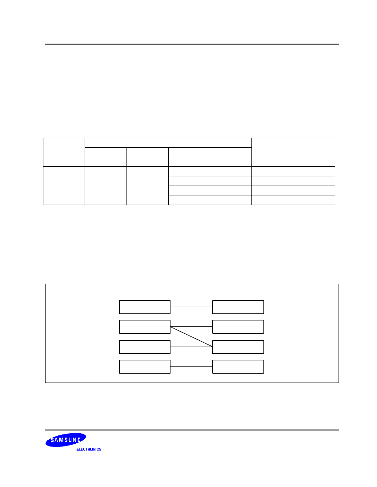
CARRY FLAG (C)
The carry flag is used to save the result of an overflow or borrow when executing arithmetic instructions involving
a carry (ADC, SBC). The carry flag can also be used as a 1-bit accumulator for performing Boolean operations
involving bit-addressed data memory.
If an overflow or borrow condition occurs when executing arithmetic instructions with carry (ADC, SBC), the carry
flag is set to "1". Otherwise, its value is "0". When a RESET occurs, the current value of the carry flag is retained
during power-down mode, but when normal operating mode resumes, its value is undefined.
The carry flag can be directly manipulated by predefined set of 1-bit read/write instructions, independent of other
bits in the PSW. Only the ADC and SBC instructions, and the instructions listed in Table 2-7, affect the carry flag.
Table 2-7. Valid Carry Flag Manipulation Instructions
Operation Type Instructions Carry Flag Manipulation
Direct manipulation SCF Set carry flag to "1"
RCF Clear carry flag to "0" (reset carry flag)
CCF Invert carry flag value (complement carry flag)
BTST C Test carry and skip if C = "1"
Bit transfer
LDB (operand)
(1)
,C
Load carry flag value to the specified bit
LDB C,(operand)
(1)
Load contents of the specified bit to carry flag
Boolean manipulation
BAND C,(operand)
(1)
AND the specified bit with contents of carry flag and save
the result to the carry flag
BOR C,(operand)
(1)
OR the specified bit with contents of carry flag and save
the result to the carry flag
BXOR C,(operand)
(1)
XOR the specified bit with contents of carry flag and save
the result to the carry flag
Interrupt routine
INTn
(2)
Save carry flag to stack with other PSW bits
Return from interrupt IRET Restore carry flag from stack with other PSW bits
NOTES:
1. The operand has three bit addressing formats: mema.a, memb.@L, and @H + DA.b.
2. “INTn” refers to the specific interrupt being executed and is not an instruction.

KS57C2308/P2308/C2316/P2316 ADDRESS SPACES
2-21
++ PROGRAMMING TIP — Using the Carry Flag as a 1-Bit Accumulator
1. Set the carry flag to logic one:
SCF ; C ← 1
LD EA,#0C3H ; EA ← #0C3H
LD HL,#0AAH ; HL ← #0AAH
ADC EA,HL ; EA ← #0C3H + #0AAH + #1H, C ← 1
2. Logical-AND bit 3 of address 3FH with P3.3 and output the result to P4.0:
LD H,#3H ; Set the upper four bits of the address to the H register
value
LDB C,@H+0FH.3 ; C ← bit 3 of 3FH
BAND C,P3.3 ; C ← C AND P3.3
LDB P4.0,C ; Output result from carry flag to P4.0

ADDRESS SPACES KS57C2308/P2308/C2316/P2316
2-22
NOTES

KS57C2308/P2308/C2316/P2316 ADDRESSING MODES
3-1
3 ADDRESSING MODES
OVERVIEW
The enable memory bank flag, EMB, controls the two addressing modes for data memory. When the EMB flag is
set to logic one, you can address the entire RAM area; when the EMB flag is cleared to logic zero, the
addressable area in the RAM is restricted to specific locations.
The EMB flag works in connection with the select memory bank instruction, SMB n. You will recall that the SMB
n instruction is used to select RAM bank 0, 1 or 15. The SMB setting is always contained in the upper four bits of
a 12-bit RAM address. For this reason, both addressing modes (EMB = "0" and EMB = "1") apply specifically to
the memory bank indicated by the SMB instruction, and any restrictions to the addressable area within banks 0, 1
or 15. Direct and indirect 1-bit, 4-bit, and 8-bit addressing methods can be used. Several RAM locations are
addressable at all times, regardless of the current EMB flag setting.
Here are a few guidelines to keep in mind regarding data memory addressing:
— When you address peripheral hardware locations in bank 15, the mnemonic for the memory-mapped
hardware component can be used as the operand in place of the actual address location.
— Always use an even-numbered RAM address as the operand in 8-bit direct and indirect addressing.
— With direct addressing, use the RAM address as the instruction operand; with indirect addressing, the
instruction specifies a register which contains the operand's address.

ADDRESSING MODES KS57C2308/P2308/C2316/P2316
3-2
DA
DA.b
@HL
@H + DA.b
@WX
@WL
mema.b memb.@L
EMB = 0 EMB = 1 X X X
000H
Working
Registers
BANK 0
(General
Registers and
Stack)
01FH
020H
0FFH
100H
1DFH
1E0H
BANK 1
(General
Registers)
RAM
Areas
Addressing
Mode
NOTES
1. 'X' means don't care.
2. Blank columns indicate RAM areas that are not addressable, given the addressing method
and enable memory bank (EMB) flag setting shown in the column headers.
EMB = 1 EMB = 0
SMB = 0 SMB = 0
SMB = 1 SMB = 1
07FH
080H
F80H
FFFH
BANK 15
(Peripheral
Hardware
Registers)
FB0H
FBFH
FC0H
SMB = 15 SMB = 15
FF0H
BANK 1
(Display Registers) SMB = 1 SMB = 1
1FFH
Figure 3-1. RAM Address Structure

KS57C2308/P2308/C2316/P2316 ADDRESSING MODES
3-3
EMB AND ERB INITIALIZATION VALUES
The EMB and ERB flag bits are set automatically by the values of the RESET vector address and the interrupt
vector address. When a RESET is generated internally, bit 7 of program memory address 0000H is written to the
EMB flag, initializing it automatically. When a vectored interrupt is generated, bit 7 of the respective vector
address table is written to the EMB. This automatically sets the EMB flag status for the interrupt service routine.
When the interrupt is serviced, the EMB value is automatically saved to stack and then restored when the
interrupt routine has completed.
At the beginning of a program, the initial EMB and ERB flag values for each vectored interrupt must be set by
using VENT instruction. The EMB and ERB can be set or reset by bit manipulation instructions (BITS, BITR)
despite the current SMB setting.
++ PROGRAMMING TIP — Initializing the EMB and ERB Flags
The following assembly instructions show how to initialize the EMB and ERB flag settings:
ORG 0000H ; ROM address assignment
VENT0 1,0,RESET
; EMB ← 1, ERB ← 0, branch RESET
VENT1 0,1,INTB
; EMB ← 0, ERB ← 1, branch INTB
VENT2 0,1,INT0
; EMB ← 0, ERB ← 1, branch INT0
VENT3 0,1,INT1
; EMB ← 0, ERB ← 1, branch INT1
VENT4 0,1,INTS
; EMB ← 0, ERB ← 1, branch INTS
VENT5 0,1,INTT0
; EMB ← 0, ERB ← 1, branch INTT0
RESET
•
•
•
BITR EMB

ADDRESSING MODES KS57C2308/P2308/C2316/P2316
3-4
ENABLE MEMORY BANK SETTINGS
EMB = "1"
When the enable memory bank flag EMB is set to logic one, you can address the data memory bank specified by
the select memory bank (SMB) value (0, 1 or 15) using 1-, 4-, or 8-bit instructions. You can use both direct and
indirect addressing modes. The addressable RAM areas when EMB = "1" are as follows:
If SMB = 0, 000H–0FFH
If SMB = 1, 100H–1FFH
If SMB = 15, F80H–FFFH
EMB = "0"
When the enable memory bank flag EMB is set to logic zero, the addressable area is defined independently of
the SMB value, and is restricted to specific locations depending on whether a direct or indirect address mode is
used.
If EMB = "0", the addressable area is restricted to locations 000H–07FH in bank 0 and to locations F80H–FFFH
in bank 15 for direct addressing. For indirect addressing, only locations 000H–0FFH in bank 0 are addressable,
regardless of SMB value.
To address the peripheral hardware register (bank 15) using indirect addressing, the EMB flag must first be set to
"1" and the SMB value to "15". When a RESET occurs, the EMB flag is set to the value contained in bit 7 of ROM
address 0000H.
EMB-Independent Addressing
At any time, several areas of the data memory can be addressed independent of the current status of the EMB
flag. These exceptions are described in Table 3-1.
Table 3-1. RAM Addressing Not Affected by the EMB Value
Address Addressing Method Affected Hardware Program Examples
000H–0FFH 4-bit indirect addressing using WX
and WL register pairs;
8-bit indirect addressing using SP
Not applicable LD
PUSH
POP
A,@WX
EA
EA
FB0H–FBFH
FF0H–FFFH
1-bit direct addressing PSW, SCMOD,
IEx, IRQx, I/O
BITS
BITR
EMB
IE4
FC0H–FFFH 1-bit indirect addressing using the
L register
BSC, I/O BTST
BAND
FC3H.@L
C,P3.@L

KS57C2308/P2308/C2316/P2316 ADDRESSING MODES
3-5
SELECT BANK REGISTER (SB)
The select bank register (SB) is used to assign the memory bank and register bank. The 8-bit SB register
consists of the 4-bit select register bank register (SRB) and the 4-bit select memory bank register (SMB), as
shown in Figure 3-2.
During interrupts and subroutine calls, SB register contents can be saved to stack in 8-bit units by the PUSH SB
instruction. You later restore the value to the SB using the POP SB instruction.
SMB 3 SMB 2 SMB 1 SMB 0 0 0 SRB 1 SRB 0
SB
REGISTER
SMB (F83H) SRB (F82H)
Figure 3-2. SMB and SRB Values in the SB Register
Select Register Bank (SRB) Instruction
The select register bank (SRB) value specifies which register bank is to be used as a working register bank. The
SRB value is set by the “SRB n” instruction, where n = 0, 1, 2, 3.
One of the four register banks is selected by the combination of ERB flag status and the SRB value that is set
using the “SRB n” instruction. The current SRB value is retained until another register is requested by program
software. PUSH SB and POP SB instructions are used to save and restore the contents of SRB during interrupts
and subroutine calls. RESET clears the 4-bit SRB value to logic zero.
Select Memory Bank (SMB) Instruction
To select one of the four available data memory banks, you must execute an SMB n instruction specifying the
number of the memory bank you want (0, 1 or 15). For example, the instruction “SMB 1” selects bank 1 and
“SMB 15” selects bank 15. (And remember to enable the selected memory bank by making the appropriate EMB
flag setting.
The upper four bits of the 12-bit data memory address are stored in the SMB register. If the SMB value is not
specified by software (or if a RESET does not occur) the current value is retained. RESET clears the 4-bit SMB
value to logic zero.
The PUSH SB and POP SB instructions save and restore the contents of the SMB register to and from the stack
area during interrupts and subroutine calls.

ADDRESSING MODES KS57C2308/P2308/C2316/P2316
3-6
DIRECT AND INDIRECT ADDRESSING
1-bit, 4-bit, and 8-bit data stored in data memory locations can be addressed directly using a specific register or
bit address as the instruction operand.
Indirect addressing specifies a memory location that contains the required direct address. The KS57 instruction
set supports 1-bit, 4-bit, and 8-bit indirect addressing. For 8-bit indirect addressing, an even-numbered RAM
address must always be used as the instruction operand.
1-BIT ADDRESSING
Table 3-2. 1-Bit Direct and Indirect RAM Addressing
Operand
Notation
Addressing Mode
Description
EMB Flag
Setting
Addressable
Area
Memory
Bank
Hardware I/O
Mapping
000H–07FH Bank 0 –
DA.b Direct: a bit is indicated by the
RAM address (DA), memory
bank selection, and a the
specified bit number (b).
0 F80H–FFFH Bank 15 All 1-bit
addressable
peripherals
(SMB = 15)
1 000H–FFFH SMB = 0, 1,
15
mema.b Direct: a bit is indicated by the
addressable area (mema) and
a the bit number (b).
x FB0H–FBFH
FF0H–FFFH
Bank 15 IS0, IS1, EMB,
ERB, IEx, IRQx,
Pn.n
memb.@L Indirect: a bit is indicated by
the addressable area
(memb.7–2 (upper) + L.3–2
(lower)) and the bit number
(L.1–0).
x FC0H–FFFH Bank 15 BSCn.x
Pn.n
@H + DA.b Indirect: a bit is indicated by
the addressable area (H
(upper) + DA.3–0 (lower)) ,
memory bank selection, and
the bit number (b).
0 000H–0FFH Bank 0 –
1 000H–FFFH SMB = 0, 1,15 All 1-bit
addressable
peripherals
(SMB = 15)
NOTE: “x” means don’t care.

KS57C2308/P2308/C2316/P2316 ADDRESSING MODES
3-7
++ PROGRAMMING TIP — 1-Bit Addressing Modes
1-Bit Direct Addressing
1. If EMB = "0":
AFLAG EQU 34H.3
BFLAG EQU 85H.3
CFLAG EQU 0BAH.0
SMB 0
BITS AFLAG ; 34H.3 ← 1
BITS BFLAG ; F85H.3 ← 1
BTST CFLAG ; If FBAH.0 = 1, skip
BITS BFLAG ; Else if, FBAH.0 = 0, F85H.3 (BMOD.3) ← 1
BITS P3.0 ; FF3H.0 (P3.0) ← 1
2. If EMB = "1":
AFLAG EQU 34H.3
BFLAG EQU 85H.3
CFLAG EQU 0BAH.0
SMB 0
BITS AFLAG ; 34H.3 ← 1
BITS BFLAG ; 85H.3 ← 1
BTST CFLAG ; If 0BAH.0 = 1, skip
BITS BFLAG ; Else if 0BAH.0 = 0, 085H.3 ← 1
BITS P3.0 ; FF3H.0 (P3.0) ← 1
1-Bit Indirect Addressing
1. If EMB = "0":
AFLAG EQU 34H.3
BFLAG EQU 85H.3
CFLAG EQU 0BAH.0
SMB 0
LD H,#0BH ; H ← #0BH
BTSTZ @H+CFLAG ; If 0BAH.0 = 1, 0BAH.0 ← 0 and skip
BITS CFLAG ; Else if 0BAH.0 = 0, FBAH.0 ← 1
2. If EMB = "1":
AFLAG EQU 34H.3
BFLAG EQU 85H.3
CFLAG EQU 0BAH.0
SMB 0
LD H,#0BH ; H ← #0BH
BTSTZ @H+CFLAG ; If 0BAH.0 = 1, 0BAH.0 ← 0 and skip
BITS CFLAG ; Else if 0BAH.0 = 0, 0BAH.0 ← 1

ADDRESSING MODES KS57C2308/P2308/C2316/P2316
3-8
4-BIT ADDRESSING
Table 3-3. 4-Bit Direct and Indirect RAM Addressing
Operand
Notation
Addressing Mode
Description
EMB Flag
Setting
Addressable
Area
Memory
Bank
Hardware I/O
Mapping
000H–07FH Bank 0 –
DA Direct: 4-bit address indicated
by the RAM address (DA) and
the memory bank selection
0 F80H–FFFH Bank 15 All 4-bit
addressable
peripherals
1 000H–FFFH SMB = 0, 1,15 (SMB = 15)
@HL Indirect: 4-bit address indi-
cated by the memory bank
selection and register HL
0 000H–0FFH Bank 0 –
1 000H–FFFH SMB = 0, 1,15All 4-bit
addressable
peripherals
(SMB = 15)
@WX Indirect: 4-bit address indi-
cated by register WX
x 000H–0FFH Bank 0 –
@WL Indirect: 4-bit address indi-
cated by register WL
x 000H–0FFH Bank 0
NOTE: “x” means don’t care.
++ PROGRAMMING TIP — 4-Bit Addressing Modes
4-Bit Direct Addressing
1. If EMB = "0":
ADATA EQU 46H
BDATA EQU 8EH
SMB 15 ; Non-essential instruction, since EMB = "0"
LD A,P3 ; A ← (P3)
SMB 0 ; Non-essential instruction, since EMB = "0"
LD ADATA,A ; (046H) ← A
LD BDATA,A ; (F8EH (LCON)) ← A
2. If EMB = "1":
ADATA EQU 46H
BDATA EQU 8EH
SMB 15
LD A,P3 ; A ← (P3)
SMB 0
LD ADATA,A ; (046H) ← A
LD BDATA,A ; (08EH) ← A

KS57C2308/P2308/C2316/P2316 ADDRESSING MODES
3-9
++ PROGRAMMING TIP — 4-Bit Addressing Modes (Continued)
4-Bit Indirect Addressing (Example 1)
1. If EMB = "0", compare bank 0 locations 040H–046H with bank 0 locations 060H–066H:
ADATA EQU 46H
BDATA EQU 66H
SMB 1 ; Non-essential instruction, since EMB = "0"
LD HL,#BDATA
LD WX,#ADATA
COMP LD A,@WL ; A ← bank 0 (040H–046H)
CPSE A,@HL ; If bank 0 (060H–066H) = A, skip
SRET
DECS L
JR COMP
RET
2. If EMB = "1", compare bank 0 locations 040H–046H to bank 1 locations 160H–166H:
ADATA EQU 46H
BDATA EQU 66H
SMB 1
LD HL,#BDATA
LD WX,#ADATA
COMP LD A,@WL ; A ← bank 0 (040H–046H)
CPSE A,@HL ; If bank 1 (160H–166H) = A, skip
SRET
DECS L
JR COMP
RET

ADDRESSING MODES KS57C2308/P2308/C2316/P2316
3-10
4-Bit Indirect Addressing (Example 2)
1. If EMB = "0", exchange bank 0 locations 040H–046H with bank 0 locations 060H–066H:
ADATA EQU 46H
BDATA EQU 66H
SMB 1 ; Non-essential instruction, since EMB = "0"
LD HL,#BDATA
LD WX,#ADATA
TRANS LD A,@WL ; A ← bank 0 (040H–046H)
XCHD A,@HL ; Bank 0 (060H–066H) ↔ A
JR TRANS
2. If EMB = "1", exchange bank 0 locations 040H–046H to bank 1 locations 160H–166H:
ADATA EQU 46H
BDATA EQU 66H
SMB 1
LD HL,#BDATA
LD WX,#ADATA
TRANS LD A,@WL ; A ← bank 0 (040H–046H)
XCHD A,@HL ; Bank 1 (160H–166H) ↔ A
JR TRANS

KS57C2308/P2308/C2316/P2316 ADDRESSING MODES
3-11
8-BIT ADDRESSING
Table 3-4. 8-Bit Direct and Indirect RAM Addressing
Instruction
Notation
Addressing Mode
Description
EMB Flag
Setting
Addressable
Area
Memory
Bank
Hardware I/O
Mapping
000H–07FH Bank 0 –
DA Direct: 8-bit address indicated
by the RAM address (DA =
even number) and memory
bank selection
0 F80H–FFFH Bank 15 All 8-bit
addressable
peripherals
1 000H–FFFH SMB = 0, 1,15(SMB = 15)
@HL Indirect: the 8-bit address indi-
cated by the memory bank
selection and register HL; (the
4-bit L register value must be
an even number)
0 000H–0FFH Bank 0 –
1 000H–FFFH SMB = 0, 1,15All 8-bit
addressable
peripherals
(SMB = 15)
++ PROGRAMMING TIP — 8-Bit Addressing Modes
8-Bit Direct Addressing
1. If EMB = "0":
ADATA EQU 46H
BDATA EQU 8EH
SMB 15 ; Non-essential instruction, since EMB = "0"
LD EA,P4 ; E ← (P5), A ← (P4)
SMB 0
LD ADATA,EA ; (046H) ← A, (047H) ← E
LD BDATA,EA ; (F8EH) ← A, (F8FH) ← E
2. If EMB = "1":
ADATA EQU 46H
BDATA EQU 8EH
SMB 15
LD EA,P4 ; E ← (P5), A ← (P4)
SMB 0
LD ADATA,EA ; (046H) ← A, (047H) ← E
LD BDATA,EA ; (08EH) ← A, (08FH) ← E

ADDRESSING MODES KS57C2308/P2308/C2316/P2316
3-12
++ PROGRAMMING TIP — 8-Bit Addressing Modes (Continued)
8-Bit Indirect Addressing
1. If EMB = "0":
ADATA EQU 46H
SMB 1 ; Non-essential instruction, since EMB = "0"
LD HL,#ADATA
LD EA,@HL ; A ← (046H), E ← (047H)
2. If EMB = "1":
ADATA EQU 46H
SMB 1
LD HL,#ADATA
LD EA,@HL ; A ← (146H), E ← (147H)

KS57C2308/P2308/C2316/P2316 MEMORY MAP
4-1
4 MEMORY MAP
OVERVIEW
To support program control of peripheral hardware, I/O addresses for peripherals are memory-mapped to bank
15 of the RAM. Memory mapping lets you use a mnemonic as the operand of an instruction in place of the
specific memory location.
Access to bank 15 is controlled by the select memory bank (SMB) instruction and by the enable memory bank
flag (EMB) setting. If the EMB flag is "0", bank 15 can be addressed using direct addressing, regardless of the
current SMB value. 1-bit direct and indirect addressing can be used for specific locations in bank 15, regardless
of the current EMB value.
I/O MAP FOR HARDWARE REGISTERS
Table 4-1 contains detailed information about I/O mapping for peripheral hardware in bank 15 (register locations
F80H–FFFH). Use the I/O map as a quick-reference source when writing application programs. The I/O map
gives you the following information:
— Register address
— Register name (mnemonic for program addressing)
— Bit values (both addressable and non-manipulable)
— Read-only, write-only, or read and write addressability
— 1-bit, 4-bit, or 8-bit data manipulation characteristics

MEMORY MAP KS57C2308/P2308/C2316/P2316
4-2
Table 4-1. I/O Map for Memory Bank 15
Memory Bank 15 Addressing Mode
Address Register Bit 3 Bit 2 Bit 1 Bit 0 R/W 1-Bit 4-Bit 8-Bit
F80H SP .3 .2 .1 "0" R/W No No Yes
F81H .7 .6 .5 .4
F82H SB “0” “0” SRB1 SRB0 – No No No
F83H SMB3 SMB2 SMB1 SMB0
Location, F84H, is not mapped.
F85H BMOD .3 .2 .1 .0 W .3 Yes No
F86H BCNT .3 .2 .1 .0 R No No Yes
F87H .7 .6 .5 .4
F88H WMOD .3 .2 .1 .0 W
.3
(1)
No Yes
F89H .7 "0" .5 .4
Locations, F8AH–F8BH, are not mapped.
F8CH LMOD .3 .2 .1 .0 W .3 No Yes
F8DH .7 .6 .5 .4
F8EH LCON “0” .2 "0" .0 W No Yes No
Location, F8FH, is not mapped.
F90H TMOD0 .3 .2 "0" "0" W .3 No Yes
F91H "0" .6 .5 .4
F92H TOE
"U"
(2)
TOE0
"U"
(2)
"U"
(2)
R/W Yes No No
Location, F93H, is not mapped.
F94H TCNT0 .3 .2 .1 .0 R No No Yes
F95H .7 .6 .5 .4
F96H TREF0 .3 .2 .1 .0 W No No Yes
F97H .7 .6 .5 .4
F98H WDMOD .3 .2 .1 .0 W No No Yes
F99H .7 .6 .5 .4
F9AH WDFLAG .3 “0” “0” “0” W Yes Yes No
Locations, F9BH–FAFH, are not mapped.
FB0H PSW IS1 IS0 EMB ERB R/W Yes Yes Yes
FB1H
C
(3)
SC2 SC1 SC0 R No No
FB2H IPR IME .2 .1 .0 W IME Yes No
FB3H PCON .3 .2 .1 .0 W No Yes No
FB4H IMOD0 .3 "0" .1 .0 W No Yes No
FB5H IMOD1 "0" "0" "0" .0
FB6H IMOD2 "0" .2 .1 .0

KS57C2308/P2308/C2316/P2316 MEMORY MAP
4-3
Table 4-1. I/O Map for Memory Bank 15 (Continued)
Memory Bank 15 Addressing Mode
Address Register Bit 3 Bit 2 Bit 1 Bit 0 R/W 1-Bit 4-Bit 8-Bit
FB7H SCMOD .3 .2 "0" .0 W Yes No No
FB8H INT (A) IE4 IRQ4 IEB IRQB R/W Yes Yes No
Location, FB9H, is not mapped
FBAH INT (B) “0” “0” IEW IRQW R/W Yes Yes No
Location, FBBH, is not mapped.
FBCH INT (C) "0" "0" IET0 IRQT0 R/W Yes Yes No
FBDH INT (D) "0" "0" IES IRQS
FBEH INT (E) IE1 IRQ1 IE0 IRQ0
FBFH INT (F) “0” “0” IE2 IRQ2
FC0H BSC0 .3 .2 .1 .0 R/W Yes Yes Yes
FC1H BSC1 .3 .2 .1 .0
FC2H BSC2 .3 .2 .1 .0
FC3H BSC3 .3 .2 .1 .0
FD0H CLMOD .3 "0" .1 .0 W No Yes No
Locations, FD1H–FD5H, are not mapped.
FD6H PNE PNE4.3 PNE4.2 PNE4.1 PNE4.0 W No No Yes
FD7H PNE5.3 PNE5.2 PNE4.1 PNE5.0
Locations, FD8H–FDBH, are not mapped.
FDCH PUMOD PM.3 PM.2 PM.1 PM.0 W No No Yes
FDDH PM.7 PM.6 PM.5 PM.4
Locations, FDEH–FDFH, are not mapped.
FE0H SMOD .3 .2 .1 .0 W .3 (R/W) No Yes
FE1H .7 .6 .5 "0"
Locations, FE2H–FE3H, are not mapped.
FE4H SBUF .3 .2 .1 .0 R/W No No Yes
FE5H .7 .6 .5 .4
Locations, FE6H–FE7H, are not mapped.
FE8H PMG1 PM3.3 PM3.2 PM3.1 PM3.0 W No No Yes
FE9H PM6.3 PM6.2 PM6.1 PM6.0
Locations, FEAH–FEBH, are not mapped.
FECH PMG2 “0” PM2 “0” “0” W No No Yes
FEDH PM7 “0” PM5 PM4
Locations, FEEH–FEFH, are not mapped.

MEMORY MAP KS57C2308/P2308/C2316/P2316
4-4
Table 4-1. I/O Map for Memory Bank 15 (Concluded)
Memory Bank 15 Addressing Mode
Address Register Bit 3 Bit 2 Bit 1 Bit 0 R/W 1-Bit 4-Bit 8-Bit
FF0H Port 0 .3 .2 .1 .0 R Yes Yes No
FF1H Port 1 .3 .2 .1 .0 R Yes Yes No
FF2H Port 2 .3 .2 .1 .0 R/W Yes Yes No
FF3H Port 3 .3 .2 .1 .0 R/W Yes Yes No
FF4H Port 4 .3 .2 .1 .0 R/W Yes Yes Yes
FF5H Port 5 .3/.7 .2/.6 .1/.5 .0/.4 R/W Yes Yes
FF6H Port 6 .3 .2 .1 .0 R/W Yes Yes Yes
FF7H Port 7 .3/.7 .2/.6 .1/.5 .0/.4 R/W Yes Yes
Locations, FF8H–FFFH, are not mapped.
NOTES:
1. Bit 3 in the WMOD register is read only.
2. “U” means that the value is unknown.
3. The carry flag can be read or written by specific bit manipulation instructions only.
REGISTER DESCRIPTIONS
In this section, register descriptions are presented in a consistent format to familiarize you with the
memory-mapped I/O locations in bank 15 of the RAM. Figure 4-1 describes the features of the register
description format. Register descriptions are arranged in alphabetical order. Programmers can use this section as
a quick-reference source when writing application programs.
Counter registers, buffer registers, and reference registers, as well as the stack pointer and port I/O latches, are
not included in these descriptions. More detailed information about how these registers are used is included in
Part II of this manual, "Hardware Descriptions”, in the context of the corresponding peripheral hardware module
descriptions.

KS57C2308/P2308/C2316/P2316 MEMORY MAP
4-5
CLMOD
− −
Clock Output Mode Control Register FD0H
Bit
Identifier
RESET
Value
Read/Write
Bit Addressing
CLMOD.3
W
4
0
3
.3
Register ID
Register name
Register location
in RAM bank 15
Bit number in
MSB to LSB order
Bit identifier used
for bit addressing
Bit value immediately
following a
RESET
Type of addressing
that must be used to
address the bit
(1-bit, 4-bit, or 8-bit)
R = Read-only
W = Write-only
R/W = Read/write
Register and bit IDs
used for bit addressing
Description of the
effect of specific
bit
Name of individual
bit or related bits
W
0
2
.2
4
W
0
1
.1
4
W
0
0
.0
4
CLMOD.2
CLMOD.1 - .0
Associated
hardware module
CPU
Bit 2
0 Always logic zero
Enable/Disable Clock Output Control Bit
01Disable clock output
Enable clock output
Clock Source and Frequency Selection Control Bits
Select CPU clock source
Select system clock fxx/8 (524 kHz at 4.19 MHz)
0
0
1
1
0
1
0
1 Select system clock fxx/64 (65.5 kHz at 4.19
Select system clock fxx/16 (262 kHz at 4.19
Figure 4-1. Register Description Format

MEMORY MAP KS57C2308/P2308/C2316/P2316
4-6
BMOD — Basic Timer Mode Register F85H
Bit
3 2 1 0
Identifier .3 .2 .1 .0
RESET Value
0 0 0 0
Read/Write
W W W W
Bit Addressing
1/4 4 4 4
.3 Basic Timer Restart Bit
1 Restart basic timer, then clear IRQB flag, BCNT and BMOD.3 to logic zero
.2–.0 Input Clock Frequency and Signal Interrupt Interval Time Control Bits
0 0 0 Input clock frequency:
Interrupt interval time (wait time):
fxx/2
12
(1.02 kHz)
220/fxx (250 ms)
0 1 1 Input clock frequency:
Interrupt interval time (wait time):
fxx/29 (8.18 kHz)
217/fxx (31.3 ms)
1 0 1 Input clock frequency:
Interrupt interval time (wait time):
fxx/27 (32.7 kHz)
215/fxx (7.82 ms)
1 1 1 Input clock frequency:
Interrupt interval time (wait time):
fxx/25 (131 kHz)
213/fxx (1.95 ms)
NOTES:
1. When a RESET occurs, the oscillator stabilization wait time is 31.3 ms (217/fxx) at 4.19 MHz.
2. “fxx” is the system clock rate given a clock frequency of 4.19 MHz.

KS57C2308/P2308/C2316/P2316 MEMORY MAP
4-7
CLMOD — Clock Output Mode Register FD0H
Bit
3 2 1 0
Identifier .3 "0" .1 .0
RESET Value
0 0 0 0
Read/Write
W W W W
Bit Addressing
4 4 4 4
.3 Enable/Disable Clock Output Control Bit
0 Disable clock output
1 Enable clock output
.2 Bit 2
0 Always logic zero
.1–.0 Clock Source and Frequency Selection Control Bits
0 0 Select CPU clock source fx/4, fx/8, fx/64, or fxt/4 (1.05 MHz, 524 kHz,
65.5 kHz, or 8.19 kHz)
0 1 Select system clock fxx/8 (524 kHz)
1 0 Select system clock fxx/16 (262 kHz)
1 1 Select system clock fxx/64 (65.5 kHz)
NOTE: “fxx” is the system clock, given a clock frequency of 4.19 MHz.

MEMORY MAP KS57C2308/P2308/C2316/P2316
4-8
IE0, 1, IRQ0, 1 — INT0, 1 Interrupt Enable/Request Flags FBEH
Bit
3 2 1 0
Identifier IE1 IRQ1 IE0 IRQ0
RESET Value
0 0 0 0
Read/Write
R/W R/W R/W R/W
Bit Addressing
1/4 1/4 1/4 1/4
IE1 INT1 Interrupt Enable Flag
0 Disable interrupt requests at the INT1 pin
1 Enable interrupt requests at the INT1 pin
IRQ1 INT1 Interrupt Request Flag
– Generate INT1 interrupt (This bit is set and cleared by hardware when rising or
falling edge detected at INT1 pin.)
IE0 INT0 Interrupt Enable Flag
0 Disable interrupt requests at the INT0 pin
1 Enable interrupt requests at the INT0 pin
IRQ0 INT0 Interrupt Request Flag
– Generate INT0 interrupt (This bit is set and cleared automatically by hardware
when rising or falling edge detected at INT0 pin.)

KS57C2308/P2308/C2316/P2316 MEMORY MAP
4-9
IE2, IRQ2 — INT2 Interrupt Enable/Request Flags FBFH
Bit
3 2 1 0
Identifier "0" "0" IE2 IRQ2
RESET Value
0 0 0 0
Read/Write
R/W R/W R/W R/W
Bit Addressing
1/4 1/4 1/4 1/4
.3–.2 Bits 3–2
0 Always logic zero
IE2 INT2 Interrupt Enable Flag
0 Disable INT2 interrupt requests at the INT2 pin
1 Enable INT2 interrupt requests at the INT2 pin
IRQ2 INT2 Interrupt Request Flag
– Generate INT2 quasi-interrupt (This bit is set and is not cleared automatically
by hardware when a rising or falling edge is detected at INT2 or KS0–KS7
respectively. Since INT2 is a quasi-interrupt, IRQ2 flag must be cleared by
software.)

MEMORY MAP KS57C2308/P2308/C2316/P2316
4-10
IE4, IRQ4 — INT4 Interrupt Enable/Request Flags FB8H
IEB, IRQB — INTB Interrupt Enable/Request Flags FB8H
Bit
3 2 1 0
Identifier IE4 IRQ4 IEB IRQB
RESET Value
0 0 0 0
Read/Write
R/W R/W R/W R/W
Bit Addressing
1/4 1/4 1/4 1/4
IE4 INT4 Interrupt Enable Flag
0 Disable interrupt requests at the INT4 pin
1 Enable interrupt requests at the INT4 pin
IRQ4 INT4 Interrupt Request Flag
– Generate INT4 interrupt (This bit is set and cleared automatically by hardware
when rising or falling signal edge detected at INT4 pin.)
IEB INTB Interrupt Enable Flag
0 Disable INTB interrupt requests
1 Enable INTB interrupt requests
IRQB INTB Interrupt Request Flag
– Generate INTB interrupt (This bit is set and cleared automatically by hardware
when reference interval signal received from basic timer.)

KS57C2308/P2308/C2316/P2316 MEMORY MAP
4-11
IES, IRQS — INTS Interrupt Enable/Request Flags FBDH
Bit
3 2 1 0
Identifier "0" "0" IES IRQS
RESET Value
0 0 0 0
Read/Write
R/W R/W R/W R/W
Bit Addressing
1/4 1/4 1/4 1/4
.3–.2 Bits 3–2
0 Always logic zero
IES INTS Interrupt Enable Flag
0 Disable INTS interrupt requests
1 Enable INTS interrupt requests
IRQS INTS Interrupt Request Flag
– Generate INTS interrupt (This bit is set and cleared automatically by hardware
when serial data transfer completion signal received from serial I/O interface.)

MEMORY MAP KS57C2308/P2308/C2316/P2316
4-12
IET0, IRQT0 — INTT0 Interrupt Enable/Request Flags FBCH
Bit
3 2 1 0
Identifier "0" "0" IET0 IRQT0
RESET Value
0 0 0 0
Read/Write
R/W R/W R/W R/W
Bit Addressing
1/4 1/4 1/4 1/4
.3–.2 Bits 3–2
0 Always logic zero
IET0 INTT0 Interrupt Enable Flag
0 Disable INTT0 interrupt requests
1 Enable INTT0 interrupt requests
IRQT0 INTT0 Interrupt Request Flag
– Generate INTT0 interrupt (This bit is set and cleared automatically by
hardware when contents of TCNT0 and TREF0 registers match.)

KS57C2308/P2308/C2316/P2316 MEMORY MAP
4-13
IEW, IRQW — INTW Interrupt Enable/Request Flags FBAH
Bit
3 2 1 0
Identifier "0" "0" IEW IRQW
RESET Value
0 0 0 0
Read/Write
R/W R/W R/W R/W
Bit Addressing
1/4 1/4 1/4 1/4
.3–.2 Bits 3–2
0 Always logic zero
IEW INTW Interrupt Enable Flag
0 Disable INTW interrupt requests
1 Enable INTW interrupt requests
IRQW INTW Interrupt Request Flag
– Generate INTW interrupt (This bit is set when the timer interval is set to 0.5
seconds or 3.91 ms.)
NOTE: Since INTW is a quasi-interrupt, the IRQW flag must be cleared by software.

MEMORY MAP KS57C2308/P2308/C2316/P2316
4-14
IMOD0 — External Interrupt 0 (INT0) Mode Register FB4H
Bit
3 2 1 0
Identifier .3 "0" .1 .0
RESET Value
0 0 0 0
Read/Write
W W W W
Bit Addressing
4 4 4 4
.3 Interrupt Sampling Clock Selection Bit
0 Select CPU clock as a sampling clock
1 Select sampling clock frequency of the selected system clock (fxx/64)
.2 Bit 2
0 Always logic zero
.1–.0 External Interrupt Mode Control Bits
0 0 Interrupt requests are triggered by a rising signal edge
0 1 Interrupt requests are triggered by a falling signal edge
1 0 Interrupt requests are triggered by both rising and falling signal edges
1 1 Interrupt request flag (IRQ0) cannot be set to logic one

KS57C2308/P2308/C2316/P2316 MEMORY MAP
4-15
IMOD1 — External Interrupt 1 (INT1) Mode Register FB5H
Bit
3 2 1 0
Identifier "0" "0" "0" IMOD1.0
RESET Value
0 0 0 0
Read/Write
W W W W
Bit Addressing
4 4 4 4
.3–.1 Bits 3–1
0 Always logic zero
.0 External Interrupt 1 Edge Detection Control Bit
0 Rising edge detection
1 Falling edge detection

MEMORY MAP KS57C2308/P2308/C2316/P2316
4-16
IMOD2 — External Interrupt 2 (INT2) Mode Register FB6H
Bit
3 2 1 0
Identifier "0" IMOD2.2 IMOD2.1 IMOD2.0
RESET Value
0 0 0 0
Read/Write
W W W W
Bit Addressing
4 4 4 4
.3 Bits 3
0 Always logic zero
.2–.0 External Interrupt 2 Edge Detection Selection Bit
0 0 0 Select rising edge at INT2 pin
0 0 1 Select falling edge at KS4–KS7
0 1 0 Select falling edge at KS2–KS7
0 1 1 Select falling edge at KS0–KS7
1 – – Ignore selection of falling edge at KS4–KS7

KS57C2308/P2308/C2316/P2316 MEMORY MAP
4-17
IPR — Interrupt Priority Register FB2H
Bit
3 2 1 0
Identifier IME .2 .1 .0
RESET Value
0 0 0 0
Read/Write
W W W W
Bit Addressing
1/4 4 4 4
IME Interrupt Master Enable Bit
0 Disable all interrupt processing
1 Enable processing for all interrupt service requests
.2–.0 Interrupt Priority Assignment Bits
0 0 0 Normal interrupt handling according to default priority settings
0 0 1 Process INTB and INT4 interrupts at highest priority
0 1 0 Process INT0 interrupts at highest priority
0 1 1 Process INT1 interrupts at highest priority
1 0 0 Process INTS interrupts at highest priority
1 0 1 Process INTT0 interrupts at highest priority

MEMORY MAP KS57C2308/P2308/C2316/P2316
4-18
LCON — LCD Output Control Register F8EH
Bit
3 2 1 0
Identifier "0" .2 "0" .0
RESET Value
0 0 0 0
Read/Write
W W W W
Bit Addressing
4 4 4 4
.3 LCD Bias Selection Bit
0 This bit is used for internal testing only; always logic zero.
.2 LCD Clock Output Disable/Enable Bit
0 Disable LCDCK and LCDSY signal outputs.
1 Enable LCDCK and LCDSY signal outputs.
.1 Bit 1
0 Always logic zero
.0 LCD Display Control Bit
0 LCD output low, turns display off: cut off current to dividing resistor, and output
port 8 latch contents.
1 If LMOD.3 = “0”, turns display off; output port 8 latch contents;
If LMOD.3 = “1”, COM and SEG output in display mode; LCD display on.
NOTES:
1. You can manipulate LCON.0, when you try to turn ON/OFF LCD display internally. If you want to control LCD
ON/OFF or LCD contrast externally, you should set the LCON.0 to "0". refer to chapter 12, if you need more
information.
2. To select the LCD bias, you must properly configure both LMOD register and the external LCD bias circuit
connection.

KS57C2308/P2308/C2316/P2316 MEMORY MAP
4-19
LMOD — LCD Mode Register F8DH, F8CH
Bit
7 6 5 4 3 2 1 0
Identifier .7 .6 .5 .4 .3 .2 .1 .0
RESET Value
0 0 0 0 0 0 0 0
Read/Write
W W W W W W W W
Bit Addressing
8 8 8 8 1/8 8 8 8
.7–.6 LCD Output Segment and Pin Configuration Bits
0 0 Segments 24–27; and 28–31
0 1 Segment 24–27; 1-bit output at P8.4–P8.7
1 0 Segment 28–31; 1-bit output at P8.0–P8.3
1 1 1-bit output only at P8.0–P8.3, and P8.4–P8.7
.5–.4 LCD Clock (LCDCK) Frequency Selection Bits
0 0
fw/29 = 64 Hz
0 1
fw/28 = 128 Hz
1 0
fw/27 = 256 Hz
1 1
fw/26 = 512 Hz
NOTE: Assuming watch timer clock (fw) = 32.768 kHz.
.3–.0 Duty and Bias Selection for LCD Display
0 – – – LCD display off
1 0 0 0 1/4 duty, 1/3 bias
1 0 0 1 1/3 duty, 1/3 bias
1 0 1 0 1/2 duty, 1/2 bias
1 0 1 1 1/3 duty, 1/2 bias
1 1 0 0 Static

MEMORY MAP KS57C2308/P2308/C2316/P2316
4-20
PCON — Power Control Register FB3H
Bit
3 2 1 0
Identifier .3 .2 .1 .0
RESET Value
0 0 0 0
Read/Write
W W W W
Bit Addressing
4 4 4 4
.3–.2 CPU Operating Mode Control Bits
0 0 Enable normal CPU operating mode
0 1 Initiate idle power-down mode
1 0 Initiate stop power-down mode
.1–.0 CPU Clock Frequency Selection Bits
0 0 If SCMOD.0 = "0", fx/64; if SCMOD.0 = "1", fxt/4
1 0 If SCMOD.0 = "0", fx/8; if SCMOD.0 = "1", fxt/4
1 1 If SCMOD.0 = "0", fx/4; if SCMOD.0 = "1", fxt/4
NOTE: “fx” is the main system clock; “fxt” is the subsystem clock.

KS57C2308/P2308/C2316/P2316 MEMORY MAP
4-21
PMG1 — Port I/O Mode Flags (Group 1: Port 3 and 6) FE9H, FE8H
Bit
7 6 5 4 3 2 1 0
Identifier PM6.3 PM6.2 PM6.1 PM6.0 PM3.3 PM3.2 PM3.1 PM3.0
RESET Value
0 0 0 0 0 0 0 0
Read/Write
W W W W W W W W
Bit Addressing
8 8 8 8 8 8 8 8
PM6.3 P6.3 I/O Mode selection Flag
0 Set P6.3 to input mode
1 Set P6.3 to output mode
PM6.2 P6.2 I/O Mode Selection Flag
0 Set P6.2 to input mode
1 Set P6.2 to output mode
PM6.1 P6.1 I/O Mode Selection Flag
0 Set P6.1 to input mode
1 Set P6.1 to output mode
PM6.0 P6.0 I/O Mode Selection Flag
0 Set P6.0 to input mode
1 Set P6.0 to output mode
PM3.3 P3.3 I/O Mode Selection Flag
0 Set P3.3 to input mode
1 Set P3.3 to output mode
PM3.2 P3.2 I/O Mode Selection Flag
0 Set P3.2 to input mode
1 Set P3.2 to output mode
PM3.1 P3.1 I/O Mode Selection Flag
0 Set P3.1 to input mode
1 Set P3.1 to output mode
PM3.0 P3.0 I/O Mode Selection Flag
0 Set P3.0 to input mode
1 Set P3.0 to output mode

MEMORY MAP KS57C2308/P2308/C2316/P2316
4-22
PMG2 — Port I/O Mode Flags (Group 2: Port 2, 4, 5, and 7) FEDH, FECH
Bit
7 6 5 4 3 2 1 0
Identifier PM7 “0” PM5 PM4 “0” PM2 “0” “0”
RESET Value
0 0 0 0 0 0 0 0
Read/Write
W W W W W W W W
Bit Addressing
8 8 8 8 8 8 8 8
PM7 P7 I/O Mode Selection Flag
0 Set P7 to input mode
1 Set P7 to output mode
.6 Bit 6
0 Always logic zero
PM5 P5 I/O Mode Selection Flag
0 Set P5 to input mode
1 Set P5 to output mode
PM4 P4 I/O Mode Selection Flag
0 Set P4 to input mode
1 Set P4 to output mode
.3 Bit 3
0 Always logic zero
PM2 P2 I/O Mode Selection Flag
0 Set P2 to input mode
1 Set P2 to output mode
.1–.0 Bits 1–0
0 Always logic zero

KS57C2308/P2308/C2316/P2316 MEMORY MAP
4-23
PNE — N-Channel Open-Drain Mode Register FD7H, FD6H
Bit
7 6 5 4 3 2 1 0
Identifier PNE5.3 PNE5.2 PNE5.1 PNE5.0 PNE4.3 PNE4.2 PNE4.1 PNE4.0
RESET Value
0 0 0 0 0 0 0 0
Read/Write
W W W W W W W W
Bit Addressing
8 8 8 8 8 8 8 8
PNE5.3 P5.3 N-Channel Open-Drain Configurable Bit
0 Configure P5.3 as a push-pull
1 Configure P5.3 as a n-channel open-drain
PNE5.2 P5.2 N-Channel Open-Drain Configurable Bit
0 Configure P5.2 as a push-pull
1 Configure P5.2 as a n-channel open-drain
PNE5.1 P5.1 N-Channel Open-Drain Configurable Bit
0 Configure P5.1 as a push-pull
1 Configure P5.1 as a n-channel open-drain
PNE5.0 P5.0 N-Channel Open-Drain Configurable Bit
0 Configure P5.0 as a push-pull
1 Configure P5.0 as a n-channel open-drain
PNE4.3 P4.3 N-Channel Open-Drain Configurable Bit
0 Configure P4.3 as a push-pull
1 Configure P4.3 as a n-channel open-drain
PNE4.2 P4.2 N-Channel Open-Drain Configurable Bit
0 Configure P4.2 as a push-pull
1 Configure P4.2 as a n-channel open-drain
PNE4.1 P4.1 N-Channel Open-Drain Configurable Bit
0 Configure P4.1 as a push-pull
1 Configure P4.1 as a n-channel open-drain
PNE4.0 P4.0 N-Channel Open-Drain Configurable Bit
0 Configure P4.0 as a push-pull
1 Configure P4.0 as a n-channel open-drain

MEMORY MAP KS57C2308/P2308/C2316/P2316
4-24
PSW — Program Status Word FB1H, FB0H
Bit
7 6 5 4 3 2 1 0
Identifier C SC2 SC1 SC0 IS1 IS0 EMB ERB
RESET Value
(1) 0 0 0 0 0 0 0
Read/Write
R/W R R R R/W R/W R/W R/W
Bit Addressing
(2) 8 8 8 1/4/8 1/4/8 1/4/8 1/4/8
C Carry Flag
0 No overflow or borrow condition exists
1 An overflow or borrow condition does exist
SC2–SC0 Skip Condition Flags
0 No skip condition exists; no direct manipulation of these bits is allowed
1 A skip condition exists; no direct manipulation of these bits is allowed
IS1, IS0 Interrupt Status Flags
0 0 Service all interrupt requests
0 1 Service only the high-priority interrupt(s) as determined in the interrupt
priority register (IPR)
1 0 Do not service any more interrupt requests
1 1 Undefined
EMB Enable Data Memory Bank Flag
0 Restrict program access to data memory to bank 15 (F80H–FFFH) and to
the locations 000H–07FH in the bank 0 only
1 Enable full access to data memory banks 0, 1, 2, and 15
ERB Enable Register Bank Flag
0 Select register bank 0 as working register area
1 Select register banks 0, 1, 2, or 3 as working register area in accordance with
the select register bank (SRB) instruction operand
NOTES:
1. The value of the carry flag after a RESET occurs during normal operation is undefined. If a RESET occurs during
power-down mode (IDLE or STOP), the current value of the carry flag is retained.
2. The carry flag can only be addressed by a specific set of 1-bit manipulation instructions. See Section 2 for
detailed information.

KS57C2308/P2308/C2316/P2316 MEMORY MAP
4-25
PUMOD — Pull-Up Resistor Mode Register FDDH, FDCH
Bit
7 6 5 4 3 2 1 0
Identifier PUR7 PUR6 PUR5 PUR4 PUR3 PUR2 PUR1 PUR0
RESET Value
0 0 0 0 0 0 0 0
Read/Write
W W W W W W W W
Bit Addressing
8 8 8 8 8 8 8 8
PUR7 Connect/Disconnect Port 7 Pull-Up Resistor Control Bit
0 Disconnect port 7 pull-up resistor
1 Connect port 7 pull-up resistor
PUR6 Connect/Disconnect Port 6 Pull-Up Resistor Control Bit
0 Disconnect port 6 pull-up resistor
1 Connect port 6 pull-up resistor
PUR5 Connect/Disconnect Port 5 Pull-Up Resistor Control Bit
0 Disconnect port 5 pull-up resistor
1 Connect port 5 pull-up resistor
PUR4 Connect/Disconnect Port 4 Pull-Up Resistor Control Bit
0 Disconnect port 4 pull-up resistor
1 Connect port 4 pull-up resistor
PUR3 Connect/Disconnect Port 3 Pull-Up Resistor Control Bit
0 Disconnect port 3 pull-up resistor
1 Connect port 3 pull-up resistor
PUR2 Connect/Disconnect Port 2 Pull-Up Resistor Control Bit
0 Disconnect port 2 pull-up resistor
1 Connect port 2 pull-up resistor
PUR1 Connect/Disconnect Port 1 Pull-Up Resistor Control Bit
0 Disconnect port 1 pull-up resistor
1 Connect port 1 pull-up resistor
PUR0 Connect/Disconnect Port 0 Pull-Up Resistor Control Bit
0 Disconnect port 0 pull-up resistor
1 Connect port 0 pull-up resistor
NOTE: Pull-up resistors for all I/O ports are automatically disabled when they are configured to output mode.

MEMORY MAP KS57C2308/P2308/C2316/P2316
4-26
SCMOD — System Clock Mode Control Register FB7H
Bit
3 2 1 0
Identifier .3 .2 "0" .0
RESET Value
0 0 0 0
Read/Write
W W W W
Bit Addressing
1 1 1 1
.3, .2 and .0 CPU Clock Selection and Main System Clock Oscillation Control Bits
0 0 0 Select main system clock (fx); enable main system clock
0 0 1 Select sub system clock (fxt); enable main system clock
0 1 0 Select main system clock (fx); disable sub system clock
1 0 1 Select sub system clock (fxt); disable main system clock
.1 Bit 1
0 Always logic zero
NOTE: SCMOD bits 3 and 0 cannot be modified simultaneously by a 4-bit instruction; they can only be modified by
separate 1-bit instructions.

KS57C2308/P2308/C2316/P2316 MEMORY MAP
4-27
SMOD — Serial I/O Mode Register FE1H, FE0H
Bit
7 6 5 4 3 2 1 0
Identifier .7 .6 .5 "0" .3 .2 .1 .0
RESET Value
0 0 0 0 0 0 0 0
Read/Write
W W W W R/W W W W
Bit Addressing
8 8 8 8 1/8 8 8 8
.7–.5 Serial I/O Clock Selection and SBUF R/W Status Control Bits
0 0 0 Use an external clock at the SCK pin;
Enable SBUF when SIO operation is halted or when SCK goes high
0 0 1 Use the TOL0 clock from timer/counter 0;
Enable SBUF when SIO operation is halted or when SCK goes high
0 1 x Use the selected CPU clock (fxx/4, 8, or 64; “fxx” is the system
clock); Enable SBUF read/write operation. “x” means “don't care.”
1 0 0
4.09 kHz clock (fxx/210)
1 1 1
262 kHz clock (fxx/24); Note: You cannot select a fxx/24 clock
frequency if you have selected a CPU clock of fxx/64
.4 Bit 4
0 Always logic zero
.3 Initiate Serial I/O Operation Bit
1 Clear IRQS flag and 3-bit clock counter to logic zero; then initiate serial
transmission. When SIO transmission starts, this bit is cleared by hardware to
logic zero
.2 Enable/Disable SIO Data Shifter and Clock Counter Bit
0 Disable the data shifter and clock counter; the contents of IRQS flag is
retained when serial transmission is completed
1 Enable the data shifter and clock counter; The IRQS flag is set to logic one
when serial transmission is completed
.1 Serial I/O Transmission Mode Selection Bit
0 Receive-only mode; output buffer is off
1 Transmit-and-receive mode; output buffer is on
.0 LSB/MSB Transmission Mode Selection Bit
0 Transmit the most significant bit (MSB) first
1 Transmit the least significant bit (LSB) first

MEMORY MAP KS57C2308/P2308/C2316/P2316
4-28
TMOD0 — Timer/Counter 0 Mode Register F91H, F90H
Bit
7 6 5 4 3 2 1 0
Identifier "0" .6 .5 .4 .3 .2 "0" "0"
RESET Value
0 0 0 0 0 0 0 0
Read/Write
W W W W W W W W
Bit Addressing
8 8 8 8 1/8 8 8 8
.7 Bit 7
0 Always logic zero
.6–.4 Timer/Counter 0 Input Clock Selection Bits
0 0 0 External clock input at TCL0 pin on rising edge
0 0 1 External clock input at TCL0 pin on falling edge
1 0 0
fxx/210 (4.09 kHz)
1 0 1
fxx/28 (16.4 kHz)
1 1 0
fxx/26 (65.5 kHz)
1 1 1
fxx/24 (262 kHz)
NOTE: “fxx” = Selected system clock of 4.19 MHz
.3 Clear Counter and Resume Counting Control Bit
1 Clear TCNT0, IRQT0, and TOL0 and resume counting immediately
(This bit is cleared automatically when counting starts.)
.2 Enable/Disable Timer/Counter 0 Bit
0 Disable timer/counter 0; retain TCNT0 contents
1 Enable timer/counter 0
.1–.0 Bit 1–0
0 Always logic zero

KS57C2308/P2308/C2316/P2316 MEMORY MAP
4-29
TOE — Timer Output Enable Flag Register F92H
Bit
3 2 1 0
Identifier “U” TOE0 “U” “U”
RESET Value
0 0 0 0
Read/Write
– R/W – –
Bit Addressing
– 1 – –
.3 Bit3
U Unknown
TOE0 Timer/Counter 0 Output Enable Flag
0 Disable timer/counter 0 output at the TCLO0 pin
1 Enable timer/counter 0 output at the TCLO0 pin
.1–.0 Bits 1–0
U Unknown

MEMORY MAP KS57C2308/P2308/C2316/P2316
4-30
WDFLAG — Watchdog Timer Counter Clear Flag Register F9AH
Bit
3 2 1 0
Identifier WDTCF “0” “0” “0”
RESET Value
0 0 0 0
Read/Write
W W W W
Bit Addressing
1/4 1/4 1/4 1/4
WDTCF Watchdog Timer Counter Clear Flag
1 Clears the watchdog timer counter
.2–.0 Bits 2–0
0 Always logic zero
NOTE: After watchdog timer is cleared by writing “1”, this bit is cleared to “0” automatically.

KS57C2308/P2308/C2316/P2316 MEMORY MAP
4-31
WDMOD — Watchdog Timer Mode Register F99H, F98H
Bit
7 6 5 4 3 2 1 0
Identifier .7 .6 .5 .4 .3 .2 .1 .0
RESET Value
1 0 1 0 0 1 0 1
Read/Write
W W W W W W W W
Bit Addressing
8 8 8 8 8 8 8 8
WDMOD Watchdog Timer Enable/Disable Control
5AH Disable watchdog timer function
Others Enable watchdog timer function

MEMORY MAP KS57C2308/P2308/C2316/P2316
4-32
WMOD — Watch Timer Mode Register F89H, F88H
Bit
7 6 5 4 3 2 1 0
Identifier .7 "0" .5 .4 .3 .2 .1 .0
RESET Value
0 0 0 0 (note) 0 0 0
Read/Write
W W W W R W W W
Bit Addressing
8 8 8 8 1 8 8 8
.7 Enable/Disable Buzzer Output Bit
0 Disable buzzer (BUZ) signal output
1 Enable buzzer (BUZ) signal output
.6 Bit 6
0 Always logic zero
.5–.4 Output Buzzer Frequency Selection Bits
0 0 2 kHz buzzer (BUZ) signal output
0 1 4 kHz buzzer (BUZ) signal output
1 0 8 kHz buzzer (BUZ) signal output
1 1 16 kHz buzzer (BUZ) signal output
.3
XTIN Input Level Control Bit
0
Input level to XT
IN
pin is low; 1-bit read-only addressable for test
1
Input level to XTIN pin is high; 1-bit read-only addressable for test
.2 Enable/Disable Watch Timer Bit
0 Disable watch timer and clear frequency dividing circuits
1 Enable watch timer
.1 Watch Timer Speed Control Bit
0 Normal speed; set IRQW to 0.5 seconds
1 High-speed operation; set IRQW to 3.91 ms
.0 Watch Timer Clock Selection Bit
0 Select the system clock (fxx/128) as the watch timer clock
1 Select a subsystem clock as the watch timer clock
NOTE: RESET sets WMOD.3 to the current input level of the subsystem clock, XTIN. If the input level is high,
WMOD.3 is set to logic one; if low, WMOD.3 is cleared to zero along with all the other bits in the WMOD
register.

KS57C2308/P2308/C2316/P2316 SAM47 INSTRUCTION SET
5-1
5 SAM47 INSTRUCTION SET
OVERVIEW
The SAM47 instruction set is specifically designed to support the large register files that are typical of most
KS57-series microcontrollers.
The SAM47 instruction set includes 1-bit, 4-bit, and 8-bit instructions for data manipulation, logical and arithmetic
operations, program control, and CPU control. I/O instructions for peripheral hardware devices are flexible and
easy to use. Symbolic hardware names can be substituted as the instruction operand in place of the actual
address. Other important features of the SAM47 instruction set include:
— 1-byte referencing of long instructions (REF instruction)
— Redundant instruction reduction (string effect)
— Skip feature for ADC and SBC instructions
Instruction operands conform to the operand format defined for each instruction. Several instructions have
multiple operand formats.
Predefined values or labels can be used as instruction operands when addressing immediate data. Many of the
symbols for specific registers and flags may also be substituted as labels for operations such DA, mema, memb,
b, and so on. Using instruction labels can greatly simplify programming and debugging tasks.
INSTRUCTION SET FEATURES
In this section, the following SAM47 instruction set features are described in detail:
— Instruction reference area
— Instruction redundancy reduction
— Flexible bit manipulation
— ADC and SBC instruction skip condition
NOTE
1. The ROM size accessed by instruction may change for different devices in the SAM47 product.
2. The number of memory bank selected by SMB may change for different devices in the SAM47 product
family.
3. The port names used instruction set may change for different devices in SAM47 product family.
4. The interrupt names and the interrupt numbers used in the instruction set may change for different
devices in the SAM47 product family.

SAM47 INSTRUCTION SET KS57C2308/P2308/C2316/P2316
5-2
Instruction Reference Area
Using the 1-byte REF (Reference) instruction, you can reference instructions stored in the addresses
0020H–007FH of program memory (the REF instruction look-up table). The location referenced by REF may
contain either two 1-byte instructions or a single 2-byte instruction. The starting address of the instruction being
referenced must always be an even number.
3-byte instructions such as JP or CALL may also be referenced using REF. To reference these 3-byte
instructions, the 2-byte pseudo commands, TJP and TCALL, must be written in the reference.
The PC is not incremented when an REF instruction is executed. After it executes, the program's instruction
execution sequence resumes at the address immediately following the REF instruction. By using REF instructions
to execute instructions larger than one byte, as well as branches and subroutines, you can reduce the program
size. To summarize, the REF instruction can be used in three ways:
— Using the 1-byte REF instruction to execute one 2-byte or two 1-byte instructions;
— Branching to any location by referencing a branch address that is stored in the look-up table;
— Calling subroutines at any location by referencing a call address that is stored in the look-up table.
If necessary, an REF instruction can be circumvented by means of a skip operation prior to the REF in the
execution sequence. In addition, the instruction immediately following an REF can also be skipped by using an
appropriate reference instruction or instructions.
Two-byte instructions can be referenced by using an REF instruction. (An exception is XCH A,DA
(note)
)
If the MSB value of the first 1-byte instruction in the reference area is “0”, the instruction cannot be referenced by
a REF instruction. Therefore, if you use REF to reference two 1-byte instructions stored in the reference area,
specific combinations must be used for the first and second 1-byte instruction. These combinations are described
in Table5-1.
Table 5-1. Valid 1-Byte Instruction Combinations for REF Look-Ups
First 1-Byte Instruction Second 1-Byte Instruction
Instruction Operand Instruction Operand
LD A,#im
INCS
(note)
R
INCS RRb
DECS
(note)
R
LD A,@Rra
INCS
(note)
R
INCS RRb
DECS
(note)
R
LD @HL,A
INCS
(note)
R
INCS RRb
DECS
(note)
R
NOTE: The MSB value of the instruction is “0”.

KS57C2308/P2308/C2316/P2316 SAM47 INSTRUCTION SET
5-3
Reducing Instruction Redundancy
When redundant instructions such as LD A,#im and LD EA,#imm are used consecutively in a program sequence,
only the first instruction is executed, but the following redundant instructions are ignored, that is, they are handled
like a NOP instruction. When LD HL,#imm instructions are used consecutively, the following redundant
instructions are also ignored.
In the following example, only the “LD A, #im” instruction will be executed. The 8-bit load instruction which
follows it is interpreted as redundant and is ignored:
LD A,#im ; Load 4-bit immediate data (#im) to accumulator
LD EA,#imm ; Load 8-bit immediate data (#imm) to extended accumulator
In this example, the statements “LD A,#2H” and “LD A,#3H” are ignored:
BITR EMB
LD A,#1H ; Execute instruction
LD A,#2H ; Ignore, redundant instruction
LD A,#3H ; Ignore, redundant instruction
LD 23H,A ; Execute instruction, 023H ← #1H
If consecutive LD HL, #imm instructions (load 8-bit immediate data to the 8-bit memory pointer pair, HL) are
detected, only the first LD is executed and the LDs which immediately follow are ignored. For example,
LD HL,#10H ; HL ← 10H
LD HL,#20H ; Ignore, redundant instruction
LD A,#3H ; A ← 3H
LD EA,#35H ; Ignore, redundant instruction
LD @HL,A ; (10H) ← 3H
If an instruction reference with a REF instruction has a redundancy effect, the following conditions apply:
— If the instruction preceding the REF has a redundancy effect, this effect is cancelled and the referenced
instruction is not skipped.
— If the instruction following the REF has a redundancy effect, the instruction following the REF is skipped.
+ + PROGRAMMING TIP — Example of the Instruction Redundancy Effect
ORG 0020H
ABC LD EA,#30H ; Stored in REF instruction reference area
ORG 0080H
•
•
•
LD EA,#40H ; Redundancy effect is encountered
REF ABC ; No skip (EA ← #30H)
•
•
•
REF ABC ; EA ← #30H
LD EA,#50H ; Skip

SAM47 INSTRUCTION SET KS57C2308/P2308/C2316/P2316
5-4
Flexible Bit Manipulation
In addition to normal bit manipulation instructions like set and clear, the SAM47 instruction set can also perform
bit tests, bit transfers, and bit Boolean operations. Bits can also be addressed and manipulated by special bit
addressing modes. Three types of bit addressing are supported:
— mema.b
— memb.@L
— @H+DA.b
The parameters of these bit addressing modes are described in more detail in Table 5-2.
Table 5-2. Bit Addressing Modes and Parameters
Addressing Mode Addressable Peripherals Address Range
mema.b ERB, EMB, IS1, IS0, IEx, IRQx FB0H–FBFH
Ports FF0H–FFFH
memb.@L Ports and BSC FC0H–FFFH
@H+DA.b All bit-manipulatable peripheral hardware All bits of the memory bank specified by
EMB and SMB that are bit-manipulatable
Instructions Which Have Skip Conditions
The following instructions have a skip function when an overflow or borrow occurs:
XCHI INCS
XCHD DECS
LDI ADS
LDD SBS
If there is an overflow or borrow from the result of an increment or decrement, a skip signal is generated and a
skip is executed. However, the carry flag value is unaffected.
The instructions BTST, BTSF, and CPSE also generate a skip signal and execute a skip when they meet a skip
condition, and the carry flag value is also unaffected.
Instructions Which Affect the Carry Flag
The only instructions which do not generate a skip signal, but which do affect the carry flag are as follows:
ADC LDB C,(operand)
SBC BAND C,(operand)
SCF BOR C,(operand)
RCF BXOR C,(operand)
CCF IRET
RRC

KS57C2308/P2308/C2316/P2316 SAM47 INSTRUCTION SET
5-5
ADC and SBC Instruction Skip Conditions
The instructions “ADC A,@HL” and “SBC A,@HL” can generate a skip signal, and set or clear the carry flag,
when they are executed in combination with the instruction “ADS A,#im”.
If an “ADS A,#im” instruction immediately follows an “ADC A,@HL” or “SBC A,@HL” instruction in a program
sequence, the ADS instruction does not skip the instruction following ADS, even if it has a skip function. If,
however, an “ADC A,@HL” or “SBC A,@HL” instruction is immediately followed by an “ADS A,#im” instruction,
the ADC (or SBC) skips on overflow (or if there is no borrow) to the instruction immediately following the ADS,
and program execution continues. Table 5-3 contains additional information and examples of the “ADC A,@HL”
and “SBC A,@HL” skip feature.
Table 5-3. Skip Conditions for ADC and SBC Instructions
Sample
Instruction Sequences
If the result of
instruction 1 is:
Then, the execution
sequence is:
Reason
ADC A,@HL
ADS A,#im
xxx
xxx
1
2
3
4
Overflow
No overflow
1, 3, 4
1, 2, 3, 4
ADS cannot skip
instruction 3, even if it
has a skip function.
SBC A,@HL
ADS A,#im
xxx
xxx
1
2
3
4
Borrow
No borrow
1, 2, 3, 4
1, 3, 4
ADS cannot skip
instruction 3, even if it
has a skip function.

SAM47 INSTRUCTION SET KS57C2308/P2308/C2316/P2316
5-6
SYMBOLS and CONVENTIONS
Table 5-4. Data Type Symbols
Symbol Data Type
d Immediate data
a Address data
b Bit data
r Register data
f Flag data
i Indirect addressing data
t
memc × 0.5 immediate data
Table 5-5. Register Identifiers
Full Register Name ID
4-bit accumulator A
4-bit working registers E, L, H, X, W,
Z, Y
8-bit extended accumulator EA
8-bit memory pointer HL
8-bit working registers WX, YZ, WL
Select register bank “n” SRB n
Select memory bank “n” SMB n
Carry flag C
Program status word PSW
Port “n” Pn
“m”-th bit of port “n” Pn.m
Interrupt priority register IPR
Enable memory bank flag EMB
Enable register bank flag ERB
Table 5-6. Instruction Operand Notation
Symbol Definition
DA Direct address
@ Indirect address prefix
src Source operand
dst Destination operand
(R) Contents of register R
.b Bit location
im 4-bit immediate data (number)
imm 8-bit immediate data (number)
# Immediate data prefix
ADR 000H–1FFFH immediate address
ADRn “n” bit address
R A, E, L, H, X, W, Z, Y
Ra E, L, H, X, W, Z, Y
RR EA, HL, WX, YZ
RRa HL, WX, WL
RRb HL, WX, YZ
RRc WX, WL
mema FB0H–FBFH, FF0H–FFFH
memb FC0H–FFFH
memc Code direct addressing:
0020H–007FH
SB Select bank register (8 bits)
XOR Logical exclusive-OR
OR Logical OR
AND Logical AND
[(RR)] Contents addressed by RR

KS57C2308/P2308/C2316/P2316 SAM47 INSTRUCTION SET
5-7
OPCODE DEFINITIONS
Table 5-7. Opcode Definitions (Direct)
Register r2 r1 r0
A 0 0 0
E 0 0 1
L 0 1 0
H 0 1 1
X 1 0 0
W 1 0 1
Z 1 1 0
Y 1 1 1
EA 0 0 0
HL 0 1 0
WX 1 0 0
YZ 1 1 0
r = Immediate data for register
Table 5-8. Opcode Definitions (Indirect)
Register i2 i1 i0
@HL 1 0 1
@WX 1 1 0
@WL 1 1 1
CALCULATING ADDITIONAL MACHINE CYCLES FOR SKIPS
A machine cycle is defined as one cycle of the selected CPU clock. Three different clock rates can be selected
using the PCON register.
In this document, the letter “S” is used in tables when describing the number of additional machine cycles
required for an instruction to execute, given that the instruction has a skip function (“S” = skip). The addition
number of machine cycles that will be required to perform the skip usually depends on the size of the instruction
being skipped — whether it is a 1-byte, 2-byte, or 3-byte instruction. A skip is also executed for SMB and SRB
instructions.
The values in additional machine cycles for “S” for the three cases in which skip conditions occur are as follows:
Case 1:No skip S = 0 cycles
Case 2:Skip is 1-byte or 2-byte instruction S = 1 cycle
Case 3:Skip is 3-byte instruction S = 2 cycles
NOTE: REF instructions are skipped in one machine cycle.
i = Immediate data for indirect addressing

SAM47 INSTRUCTION SET KS57C2308/P2308/C2316/P2316
5-8
HIGH-LEVEL SUMMARY
This section contains a high-level summary of the SAM47 instruction set in table format. The tables are designed
to familiarize you with the range of instructions that are available in each instruction category.
These tables are a useful quick-reference resource when writing application programs.
If you are reading this user's manual for the first time, however, you may want to scan this detailed information
briefly, and then return to it later on. The following information is provided for each instruction:
— Instruction name
— Operand(s)
— Brief operation description
— Number of bytes of the instruction and operand(s)
— Number of machine cycles required to execute the instruction
The tables in this section are arranged according to the following instruction categories:
— CPU control instructions
— Program control instructions
— Data transfer instructions
— Logic instructions
— Arithmetic instructions
— Bit manipulation instructions

KS57C2308/P2308/C2316/P2316 SAM47 INSTRUCTION SET
5-9
Table 5-9. CPU Control Instructions — High-Level Summary
Name Operand Operation Description Bytes Cycles
SCF Set carry flag to logic one 1 1
RCF Reset carry flag to logic zero 1 1
CCF Complement carry flag 1 1
EI Enable all interrupts 2 2
DI Disable all interrupts 2 2
IDLE Engage CPU idle mode 2 2
STOP Engage CPU stop mode 2 2
NOP No operation 1 1
SMB n Select memory bank 2 2
SRB n Select register bank 2 2
REF memc Reference code 1 1
VENTn EMB (0,1)
ERB (0,1)
ADR
Load enable memory bank flag (EMB) and the enable
register bank flag (ERB) and program counter to vector
address, then branch to the corresponding location
2 2
Table 5-10. Program Control Instructions — High-Level Summary
Name Operand Operation Description Bytes Cycles
CPSE R,#im Compare and skip if register equals #im 2 2 + S
@HL,#im Compare and skip if indirect data memory equals #im 2 2 + S
A,R Compare and skip if A equals R 2 2 + S
A,@HL Compare and skip if A equals indirect data memory 1 1 + S
EA,@HL Compare and skip if EA equals indirect data memory 2 2 + S
EA,RR Compare and skip if EA equals RR 2 2 + S
JP ADR14 Jump to direct address (14 bits) 3 3
JPS ADR12 Jump direct in page (12 bits) 2 2
JR #im Jump to immediate address 1 2
@WX Branch relative to WX register 2 3
@EA Branch relative to EA 2 3
CALL ADR14 Call direct in page (14 bits) 3 4
CALLS ADR11 Call direct in page (11 bits) 2 3
RET – Return from subroutine 1 3
IRET – Return from interrupt 1 3
SRET – Return from subroutine and skip 1 3 + S

SAM47 INSTRUCTION SET KS57C2308/P2308/C2316/P2316
5-10
Table 5-11. Data Transfer Instructions — High-Level Summary
Name Operand Operation Description Bytes Cycles
XCH A,DA Exchange A and direct data memory contents 2 2
A,Ra Exchange A and register (Ra) contents 1 1
A,@RRa Exchange A and indirect data memory 1 1
EA,DA Exchange EA and direct data memory contents 2 2
EA,RRb Exchange EA and register pair (RRb) contents 2 2
EA,@HL Exchange EA and indirect data memory contents 2 2
XCHI A,@HL Exchange A and indirect data memory contents;
increment contents of register L and skip on carry
1 2 + S
XCHD A,@HL Exchange A and indirect data memory contents;
decrement contents of register L and skip on carry
1 2 + S
LD A,#im Load 4-bit immediate data to A 1 1
A,@RRa Load indirect data memory contents to A 1 1
A,DA Load direct data memory contents to A 2 2
A,Ra Load register contents to A 2 2
Ra,#im Load 4-bit immediate data to register 2 2
RR,#imm Load 8-bit immediate data to register 2 2
DA,A Load contents of A to direct data memory 2 2
Ra,A Load contents of A to register 2 2
EA,@HL Load indirect data memory contents to EA 2 2
EA,DA Load direct data memory contents to EA 2 2
EA,RRb Load register contents to EA 2 2
@HL,A Load contents of A to indirect data memory 1 1
DA,EA Load contents of EA to data memory 2 2
RRb,EA Load contents of EA to register 2 2
@HL,EA Load contents of EA to indirect data memory 2 2
LDI A,@HL Load indirect data memory to A; increment register L
contents and skip on carry
1 2 + S
LDD A,@HL Load indirect data memory contents to A; decrement
register L contents and skip on carry
1 2 + S
LDC EA,@WX Load code byte from WX to EA 1 3
EA,@EA Load code byte from EA to EA 1 3
RRC A Rotate right through carry bit 1 1
PUSH RR Push register pair onto stack 1 1
SB Push SMB and SRB values onto stack 2 2
POP RR Pop to register pair from stack 1 1
SB Pop SMB and SRB values from stack 2 2

KS57C2308/P2308/C2316/P2316 SAM47 INSTRUCTION SET
5-11
Table 5-12. Logic Instructions — High-Level Summary
Name Operand Operation Description Bytes Cycles
AND A,#im Logical-AND A immediate data to A 2 2
A,@HL Logical-AND A indirect data memory to A 1 1
EA,RR Logical-AND register pair (RR) to EA 2 2
RRb,EA Logical-AND EA to register pair (RRb) 2 2
OR A, #im Logical-OR immediate data to A 2 2
A, @HL Logical-OR indirect data memory contents to A 1 1
EA,RR Logical-OR double register to EA 2 2
RRb,EA Logical-OR EA to double register 2 2
XOR A,#im Exclusive-OR immediate data to A 2 2
A,@HL Exclusive-OR indirect data memory to A 1 1
EA,RR Exclusive-OR register pair (RR) to EA 2 2
RRb,EA Exclusive-OR register pair (RRb) to EA 2 2
COM A Complement accumulator (A) 2 2
Table 5-13. Arithmetic Instructions — High-Level Summary
Name Operand Operation Description Bytes Cycles
ADC A,@HL Add indirect data memory to A with carry 1 1
EA,RR Add register pair (RR) to EA with carry 2 2
RRb,EA Add EA to register pair (RRb) with carry 2 2
ADS A, #im Add 4-bit immediate data to A and skip on carry 1 1 + S
EA,#imm Add 8-bit immediate data to EA and skip on carry 2 2 + S
A,@HL Add indirect data memory to A and skip on carry 1 1 + S
EA,RR Add register pair (RR) contents to EA and skip on carry 2 2 + S
RRb,EA Add EA to register pair (RRb) and skip on carry 2 2 + S
SBC A,@HL Subtract indirect data memory from A with carry 1 1
EA,RR Subtract register pair (RR) from EA with carry 2 2
RRb,EA Subtract EA from register pair (RRb) with carry 2 2
SBS A,@HL Subtract indirect data memory from A; skip on borrow 1 1 + S
EA,RR Subtract register pair (RR) from EA; skip on borrow 2 2 + S
RRb,EA Subtract EA from register pair (RRb); skip on borrow 2 2 + S
DECS R Decrement register (R); skip on borrow 1 1 + S
RR Decrement register pair (RR); skip on borrow 2 2 + S
INCS R Increment register (R); skip on carry 1 1 + S
DA Increment direct data memory; skip on carry 2 2 + S
@HL Increment indirect data memory; skip on carry 2 2 + S
RRb Increment register pair (RRb); skip on carry 1 1 + S

SAM47 INSTRUCTION SET KS57C2308/P2308/C2316/P2316
5-12
Table 5-14. Bit Manipulation Instructions — High-Level Summary
Name Operand Operation Description Bytes Cycles
BTST C Test specified bit and skip if carry flag is set 1 1 + S
DA.b Test specified bit and skip if memory bit is set
mema.b
memb.@L
@H+DA.b
BTSF DA.b Test specified memory bit and skip if bit equals "0"
mema.b 2 2 + S
memb.@L
@H+DA.b
BTSTZ mema.b Test specified bit; skip and clear if memory bit is set
memb.@L
@H+DA.b
BITS DA.b Set specified memory bit
mema.b
memb.@L
@H+DA.b
BITR DA.b Clear specified memory bit to logic zero
mema.b
memb.@L
@H+DA.b
BAND C,mema.b Logical-AND carry flag with specified memory bit
C,memb.@L
C,@H+DA.b 2 2
BOR C,mema.b Logical-OR carry with specified memory bit
C,memb.@L
C,@H+DA.b
BXOR C,mema.b Exclusive-OR carry with specified memory bit
C,memb.@L
C,@H+DA.b
LDB mema.b,C Load carry bit to a specified memory bit
memb.@L,C Load carry bit to a specified indirect memory bit
@H+DA.b,C
C,mema.b Load specified memory bit to carry bit
C,memb.@L Load specified indirect memory bit to carry bit
C,@H+DA.b

KS57C2308/P2308/C2316/P2316 SAM47 INSTRUCTION SET
5-13
BINARY CODE SUMMARY
This section contains binary code values and operation notation for each instruction in the SAM47 instruction set
in an easy-to-read, tabular format. It is intended to be used as a quick-reference source for programmers who are
experienced with the SAM47 instruction set. The same binary values and notation are also included in the
detailed descriptions of individual instructions later in Section 5.
If you are reading this user's manual for the first time, please just scan this very detailed information briefly. Most
of the general information you will need to write application programs can be found in the high-level summary
tables in the previous section. The following information is provided for each instruction:
— Instruction name
— Operand(s)
— Binary values
— Operation notation
The tables in this section are arranged according to the following instruction categories:
— CPU control instructions
— Program control instructions
— Data transfer instructions
— Logic instructions
— Arithmetic instructions
— Bit manipulation instructions

SAM47 INSTRUCTION SET KS57C2308/P2308/C2316/P2316
5-14
Table 5-15. CPU Control Instructions — Binary Code Summary
Name Operand Binary Code Operation Notation
SCF 1 1 1 0 0 1 1 1
C ← 1
RCF 1 1 1 0 0 1 1 0
C ← 0
CCF 1 1 0 1 0 1 1 0
C ← C
EI 1 1 1 1 1 1 1 1
IME ← 1
1 0 1 1 0 0 1 0
DI 1 1 1 1 1 1 1 0
IME ← 0
1 0 1 1 0 0 1 0
IDLE 1 1 1 1 1 1 1 1
PCON.2 ← 1
1 0 1 0 0 0 1 1
STOP 1 1 1 1 1 1 1 1
PCON.3 ← 1
1 0 1 1 0 0 1 1
NOP 1 0 1 0 0 0 0 0 No operation
SMB n 1 1 0 1 1 1 0 1
SMB ← n
0 1 0 0 d3 d2 d1 d0
SRB n 1 1 0 1 1 1 0 1
SRB ← n (n = 0, 1, 2, 3)
0 1 0 1 0 0 d1 d0
REF memc t7 t6 t5 t4 t3 t2 t1 t0
PC13 – 0 ← memc5 – 0 + (memc + 1),
7 – 0
VENTn EMB (0,1)
ERB (0,1)
ADR
E
M
B
E
R
B
a13 a12 a11 a10 a9 a8
ROM (2 x n) 7–6 ← EMB, ERB
ROM (2 x n) 5–4 ← PC13–12
ROM (2 x n) 3–0 ← PC11–8
ROM (2 x n + 1) 7–0 ← PC7–0
(n = 0, 1, 2, 3, 4, 5, 6, 7)
a7 a6 a5 a4 a3 a2 a1 a0

KS57C2308/P2308/C2316/P2316 SAM47 INSTRUCTION SET
5-15
Table 5-16. Program Control Instructions — Binary Code Summary
Name Operand Binary Code Operation Notation
CPSE R,#im 1 1 0 1 1 0 0 1 Skip if R = im
d3 d2 d1 d0 0 r2 r1 r0
@HL,#im 1 1 0 1 1 1 0 1 Skip if (HL) = im
0 1 1 1 d3 d2 d1 d0
A,R 1 1 0 1 1 1 0 1 Skip if A = R
0 1 1 0 1 r2 r1 r0
A,@HL 0 0 1 1 1 0 0 0 Skip if A = (HL)
EA,@HL 1 1 0 1 1 1 0 0 Skip if A = (HL), E = (HL+1)
0 0 0 0 1 0 0 1
EA,RR 1 1 0 1 1 1 0 0 Skip if EA = RR
1 1 1 0 1 r2 r1 0
JP ADR14 1 1 0 1 1 0 1 1
PC13–0 ← ADR13–0
0 0 a13 a12 a11 a10 a9 a8
a7 a6 a5 a4 a3 a2 a1 a0
JPS ADR12 1 0 0 1 a11 a10 a9 a8
PC13–0 ← PC13–12 + ADR11–0
a7 a6 a5 a4 a3 a2 a1 a0
JR
#im *
PC13–0 ← ADR (PC–15 to PC+16)
@WX 1 1 0 1 1 1 0 1
PC13–0 ← PC13–8 + (WX)
0 1 1 0 0 1 0 0
@EA 1 1 0 1 1 1 0 1
PC13–0 ← PC13–8 + (EA)
0 1 1 0 0 0 0 0
CALL ADR14 1 1 0 1 1 0 1 1
[(SP–1) (SP–2)] ← EMB, ERB
0 1 a13 a12 a11 a10 a9 a8
[(SP–3) (SP–4)] ← PC7–0
[(SP–5) (SP–6)] ← PC13–8
a7 a6 a5 a4 a3 a2 a1 a0
PC13–0 ← ADR13–0
(SP) ← (SP)–6
CALLS ADR11 1 1 1 0 1 a10 a9 a8
[(SP–1) (SP–2)] ← EMB, ERB
[(SP–3) (SP–4)] ← PC7–0
[(SP–5) (SP–6)] ← PC10–8
a7 a6 a5 a4 a3 a2 a1 a0
PC13–11 ← 00
PC10–0 ← ADR10–0
(SP) ← (SP)–6
First Byte Condition
* JR #im
0 0 0 1 a3 a2 a1 a0
PC ← PC+2 to PC+16
0 0 0 0 a3 a2 a1 a0
PC ← PC–1 to PC–15

SAM47 INSTRUCTION SET KS57C2308/P2308/C2316/P2316
5-16
Table 5-16. Program Control Instructions — Binary Code Summary (Continued)
Name Operand Binary Code Operation Notation
RET – 1 1 0 0 0 1 0 1
PC13–8 ← (SP + 1) (SP)
PC7–0← (SP + 2) (SP + 3)
EMB,ERB ← (SP + 5) (SP + 4)
SP ← SP + 6
IRET – 1 1 0 1 0 1 0 1
PC13–8 ← (SP + 1) (SP)
PC7–0 ← (SP + 2) (SP + 3)
PSW ← (SP + 4) (SP + 5)
SP ← SP + 6
SRET – 1 1 1 0 0 1 0 1
PC13–8 ← (SP + 1) (SP)
PC7–0 ← (SP + 3) (SP + 2)
EMB,ERB ← (SP + 5) (SP + 4)
SP ← SP + 6, then skip
Table 5-17. Data Transfer Instructions — Binary Code Summary
Name Operand Binary Code Operation Notation
XCH A,DA 0 1 1 1 1 0 0 1
A ↔ DA
a7 a6 a5 a4 a3 a2 a1 a0
A,Ra 0 1 1 0 1 r2 r1 r0
A ↔ Ra
A,@RRa 0 1 1 1 1 i2 i1 i0
A ↔ (RRa)
EA,DA 1 1 0 0 1 1 1 1
A ↔ DA,E ↔ DA + 1
a7 a6 a5 a4 a3 a2 a1 a0
EA,RRb 1 1 0 1 1 1 0 0
EA ↔ RRb
1 1 1 0 0 r2 r1 0
EA,@HL 1 1 0 1 1 1 0 0
A ↔ (HL), E ↔ (HL + 1)
0 0 0 0 0 0 0 1
XCHI A,@HL 0 1 1 1 1 0 1 0
A ↔ (HL), then L ← L+1;
skip if L = 0H
XCHD A,@HL 0 1 1 1 1 0 1 1
A ↔ (HL), then L ← L-1;
skip if L = 0FH
LD A,#im 1 0 1 1 d3 d2 d1 d0
A ← im
A,@RRa 1 0 0 0 1 i2 i1 i0
A ← (RRa)
A,DA 1 0 0 0 1 1 0 0
A ← DA
a7 a6 a5 a4 a3 a2 a1 a0
A,Ra 1 1 0 1 1 1 0 1
A ← Ra
0 0 0 0 1 r2 r1 r0

KS57C2308/P2308/C2316/P2316 SAM47 INSTRUCTION SET
5-17
Table 5-17. Data Transfer Instructions — Binary Code Summary (Continued)
Name Operand Binary Code Operation Notation
LD Ra,#im 1 1 0 1 1 0 0 1
Ra ← im
d3 d2 d1 d0 1 r2 r1 r0
RR,#imm 1 0 0 0 0 r2 r1 1
RR ← imm
d7 d6 d5 d4 d3 d2 d1 d0
DA,A 1 0 0 0 1 0 0 1
DA ← A
a7 a6 a5 a4 a3 a2 a1 a0
Ra,A 1 1 0 1 1 1 0 1
Ra ← A
0 0 0 0 0 r2 r1 r0
EA,@HL 1 1 0 1 1 1 0 0
A ← (HL), E ← (HL + 1)
0 0 0 0 1 0 0 0
EA,DA 1 1 0 0 1 1 1 0
A ← DA, E ← DA + 1
a7 a6 a5 a4 a3 a2 a1 a0
EA,RRb 1 1 0 1 1 1 0 0
EA ← RRb
1 1 1 1 1 r2 r1 0
@HL,A 1 1 0 0 0 1 0 0
(HL) ← A
DA,EA 1 1 0 0 1 1 0 1
DA ← A, DA + 1 ←E
a7 a6 a5 a4 a3 a2 a1 a0
RRb,EA 1 1 0 1 1 1 0 0
RRb ← EA
1 1 1 1 0 r2 r1 0
@HL,EA 1 1 0 1 1 1 0 0
(HL) ← A, (HL + 1) ← E
0 0 0 0 0 0 0 0
LDI A,@HL 1 0 0 0 1 0 1 0
A ← (HL), then L ← L+1;
skip if L = 0H
LDD A,@HL 1 0 0 0 1 0 1 1
A ← (HL), then L ← L–1;
skip if L = 0FH
LDC EA,@WX 1 1 0 0 1 1 0 0
EA ← [PC13–8 + (WX)]
EA,@EA 1 1 0 0 1 0 0 0
EA ← [PC13–8 + (EA)]
RRC A 1 0 0 0 1 0 0 0
C ← A.0, A3 ← C
A.n–1 ← A.n (n = 1, 2, 3)
PUSH RR 0 0 1 0 1 r2 r1 1
((SP–1)) ((SP–2)) ← (RR),
(SP) ← (SP)–2
SB 1 1 0 1 1 1 0 1
((SP–1)) ← (SMB), ((SP–2)) ←(SRB),
(SP) ← (SP)–2
0 1 1 0 0 1 1 1

SAM47 INSTRUCTION SET KS57C2308/P2308/C2316/P2316
5-18
Table 5-17. Data Transfer Instructions — Binary Code Summary (Concluded)
Name Operand Binary Code Operation Notation
POP RR 0 0 1 0 1 r2 r1 0
RRL ← (SP), RRH ← (SP + 1)
SP ← SP + 2
SB 1 1 0 1 1 1 0 1
(SRB) ← (SP), SMB ← (SP + 1),
SP ← SP + 2
0 1 1 0 0 1 1 0
Table 5-18. Logic Instructions — Binary Code Summary
Name Operand Binary Code Operation Notation
AND A,#im 1 1 0 1 1 1 0 1
A ← A AND im
0 0 0 1 d3 d2 d1 d0
A,@HL 0 0 1 1 1 0 0 1
A ← A AND (HL)
EA,RR 1 1 0 1 1 1 0 0
EA ← EA AND RR
0 0 0 1 1 r2 r1 0
RRb,EA 1 1 0 1 1 1 0 0
RRb ← RRb AND EA
0 0 0 1 0 r2 r1 0
OR A, #im 1 1 0 1 1 1 0 1
A ← A OR im
0 0 1 0 d3 d2 d1 d0
A, @HL 0 0 1 1 1 0 1 0
A ← A OR (HL)
EA,RR 1 1 0 1 1 1 0 0
EA ← EA OR RR
0 0 1 0 1 r2 r1 0
RRb,EA 1 1 0 1 1 1 0 0
RRb ← RRb OR EA
0 0 1 0 0 r2 r1 0
XOR A,#im 1 1 0 1 1 1 0 1
A ← A XOR im
0 0 1 1 d3 d2 d1 d0
A,@HL 0 0 1 1 1 0 1 1
A ← A XOR (HL)
EA,RR 1 1 0 1 1 1 0 0
EA ← EA XOR (RR)
0 0 1 1 0 r2 r1 0
RRb,EA 1 1 0 1 1 1 0 0
RRb ← RRb XOR EA
0 0 1 1 0 r2 r1 0
COM A 1 1 0 1 1 1 0 1
A ← A
0 0 1 1 1 1 1 1

KS57C2308/P2308/C2316/P2316 SAM47 INSTRUCTION SET
5-19
Table 5-19. Arithmetic Instructions — Binary Code Summary
Name Operand Binary Code Operation Notation
ADC A,@HL 0 0 1 1 1 1 1 0
C, A ← A + (HL) + C
EA,RR 1 1 0 1 1 1 0 0
C, EA ← EA + RR + C
1 0 1 0 1 r2 r1 0
RRb,EA 1 1 0 1 1 1 0 0
C, RRb ← RRb + EA + C
1 0 1 0 0 r2 r1 0
ADS A, #im 1 0 1 0 d3 d2 d1 d0
A ← A + im; skip on carry
EA,#imm 1 1 0 0 1 0 0 1
EA ← EA + imm; skip on carry
d7 d6 d5 d4 d3 d2 d1 d0
A,@HL 0 0 1 1 1 1 1 1
A ← A+ (HL); skip on carry
EA,RR 1 1 0 1 1 1 0 0
EA ← EA + RR; skip on carry
1 0 0 1 1 r2 r1 0
RRb,EA 1 1 0 1 1 1 0 0
RRb ← RRb + EA; skip on carry
1 0 0 1 0 r2 r1 0
SBC A,@HL 0 0 1 1 1 1 0 0
C,A ← A – (HL) – C
EA,RR 1 1 0 1 1 1 0 0
C, EA ← EA –RR – C
1 1 0 0 1 r2 r1 0
RRb,EA 1 1 0 1 1 1 0 0
C,RRb ← RRb – EA – C
1 1 0 0 0 r2 r1 0
SBS A,@HL 0 0 1 1 1 1 0 1
A ← A – (HL); skip on borrow
EA,RR 1 1 0 1 1 1 0 0
EA ← EA – RR; skip on borrow
1 0 1 1 1 r2 r1 0
RRb,EA 1 1 0 1 1 1 0 0
RRb ← RRb – EA; skip on borrow
1 0 1 1 0 r2 r1 0
DECS R 0 1 0 0 1 r2 r1 r0
R ← R–1; skip on borrow
RR 1 1 0 1 1 1 0 0
RR ← RR–1; skip on borrow
1 1 0 1 1 r2 r1 0
INCS R 0 1 0 1 1 r2 r1 r0
R ← R + 1; skip on carry
DA 1 1 0 0 1 0 1 0
DA ← DA + 1; skip on carry
a7 a6 a5 a4 a3 a2 a1 a0
@HL 1 1 0 1 1 1 0 1
(HL) ← (HL) + 1; skip on carry
0 1 1 0 0 0 1 0
RRb 1 0 0 0 0 r2 r1 0
RRb ← RRb + 1; skip on carry

SAM47 INSTRUCTION SET KS57C2308/P2308/C2316/P2316
5-20
Table 5-20. Bit Manipulation Instructions — Binary Code Summary
Name Operand Binary Code Operation Notation
BTST C 1 1 0 1 0 1 1 1 Skip if C = 1
DA.b 1 1 b1 b0 0 0 1 1 Skip if DA.b = 1
a7 a6 a5 a4 a3 a2 a1 a0
mema.b *
1 1 1 1 1 0 0 1 Skip if mema.b = 1
memb.@L 1 1 1 1 1 0 0 1 Skip if [memb.7–2 + L.3–2].
[L.1–0] = 1
0 1 0 0 a5 a4 a3 a2
@H+DA.b 1 1 1 1 1 0 0 1 Skip if [H + DA.3–0].b = 1
0 0 b1 b0 a3 a2 a1 a0
BTSF DA.b 1 1 b1 b0 0 0 1 0 Skip if DA.b = 0
a7 a6 a5 a4 a3 a2 a1 a0
mema.b *
1 1 1 1 1 0 0 0 Skip if mema.b = 0
memb.@L 1 1 1 1 1 0 0 0 Skip if [memb.7–2 + L.3–2].
[L.1–0] = 0
0 1 0 0 a5 a4 a3 a2
@H DA.b 1 1 1 1 1 0 0 0 Skip if [H + DA.3–0].b = 0
0 0 b1 b0 a3 a2 a1 a0
BTSTZ
mema.b *
1 1 1 1 1 1 0 1 Skip if mema.b = 1 and clear
memb.@L 1 1 1 1 1 1 0 1 Skip if [memb.7–2 + L.3–2].
[L.1–0] = 1 and clear
0 1 0 0 a5 a4 a3 a2
@H+DA.b 1 1 1 1 1 1 0 1 Skip if [H + DA.3–0].b =1 and clear
0 0 b1 b0 a3 a2 a1 a0
BITS DA.b 1 1 b1 b0 0 0 0 1
DA.b ← 1
a7 a6 a5 a4 a3 a2 a1 a0
mema.b *
1 1 1 1 1 1 1 1
mema.b ← 1
memb.@L 1 1 1 1 1 1 1 1
[memb.7–2 + L.3–2].[L.1–0] ← 1
0 1 0 0 a5 a4 a3 a2
@H+DA.b 1 1 1 1 1 1 1 1
[H + DA.3–0].b ← 1
0 0 b1 b0 a3 a2 a1 a0

KS57C2308/P2308/C2316/P2316 SAM47 INSTRUCTION SET
5-21
Table 5-20. Bit Manipulation Instructions — Binary Code Summary (Continued)
Name Operand Binary Code Operation Notation
BITR DA.b 1 1 b1 b0 0 0 0 0
DA.b ← 0
a7 a6 a5 a4 a3 a2 a1 a0
mema.b *
1 1 1 1 1 1 1 0
mema.b ← 0
memb.@L 1 1 1 1 1 1 1 0
[memb.7–2 + L3–2].[L.1–0] ← 0
0 1 0 0 a5 a4 a3 a2
@H+DA.b 1 1 1 1 1 1 1 0
[H + DA.3–0].b ← 0
0 0 b1 b0 a3 a2 a1 a0
BAND
C,mema.b *
1 1 1 1 0 1 0 1
C ← C AND mema.b
C,memb.@L 1 1 1 1 0 1 0 1
C ← C AND [memb.7–2 + L.3–2].
[L.1–0]
0 1 0 0 a5 a4 a3 a2
C,@H+DA.b 1 1 1 1 0 1 0 1
C ← C AND [H + DA.3–0].b
0 0 b1 b0 a3 a2 a1 a0
BOR
C,mema.b *
1 1 1 1 0 1 1 0
C ← C OR mema.b
C,memb.@L 1 1 1 1 0 1 1 0
C ← C OR [memb.7–2 + L.3–2].
[L.1–0]
0 1 0 0 a5 a4 a3 a2
C,@H+DA.b 1 1 1 1 0 1 1 0
C ← C OR [H + DA.3–0].b
0 0 b1 b0 a3 a2 a1 a0
BXOR
C,mema.b *
1 1 1 1 0 1 1 1
C ← C XOR mema.b
C,memb.@L 1 1 1 1 0 1 1 1
C ← C XOR [memb.7–2 + L.3–2].
[L.1–0]
0 1 0 0 a5 a4 a3 a2
C,@H+DA.b 1 1 1 1 0 1 1 1
C ← C XOR [H + DA.3–0].b
0 0 b1 b0 a3 a2 a1 a0
Second Byte Bit Addresses
* mema.b
1 0 b1 b0 a3 a2 a1 a0 FB0H–FBFH
1 1 b1 b0 a3 a2 a1 a0 FF0H–FFFH

SAM47 INSTRUCTION SET KS57C2308/P2308/C2316/P2316
5-22
Table 5-20. Bit Manipulation Instructions — Binary Code Summary (Concluded)
Name Operand Binary Code Operation Notation
LDB
mema.b,C *
1 1 1 1 1 1 0 0
mema.b ← C
memb.@L,C 1 1 1 1 1 1 0 0
memb.7–2 + [L.3–2]. [L.1–0] ← C
0 1 0 0 a5 a4 a3 a2
@H+DA.b,C 1 1 1 1 1 1 0 0
H + [DA.3–0].b ← (C)
0 0 b1 b0 a3 a2 a1 a0
C,mema.b *
1 1 1 1 0 1 0 0
C ← mema.b
C,memb.@L 1 1 1 1 0 1 0 0
C ← memb.7–2 + [L.3–2] . [L.1–0]
0 1 0 0 a5 a4 a3 a2
C,@H+DA.b 1 1 1 1 0 1 0 0
C ← [H + DA.3–0].b
0 0 b1 b0 a3 a2 a1 a0
Second Byte Bit Addresses
* mema.b
1 0 b1 b0 a3 a2 a1 a0 FB0H–FBFH
1 1 b1 b0 a3 a2 a1 a0 FF0H–FFFH

KS57C2308/P2308/C2316/P2316 SAM47 INSTRUCTION SET
5-23
INSTRUCTION DESCRIPTIONS
This section contains detailed information and programming examples for each instruction of the SAM47
instruction set. Information is arranged in a consistent format to improve readability and for use as a
quick-reference resource for application programmers.
If you are reading this user's manual for the first time, please just scan this very detailed information briefly in
order to acquaint yourself with the basic features of the instruction set. The information elements of the
instruction description format are as follows:
— Instruction name (mnemonic)
— Full instruction name
— Source/destination format of the instruction operand
— Operation overview (from the "High-Level Summary" table)
— Textual description of the instruction's effect
— Binary code overview (from the "Binary Code Summary" table)
— Programming example(s) to show how the instruction is used

SAM47 INSTRUCTION SET KS57C2308/P2308/C2316/P2316
5-24
ADC — Add With Carry
ADC dst,src
Operation: Operand Operation Summary Bytes Cycles
A,@HL Add indirect data memory to A with carry 1 1
EA,RR Add register pair (RR) to EA with carry 2 2
RRb,EA Add EA to register pair (RRb) with carry 2 2
Description: The source operand, along with the setting of the carry flag, is added to the destination operand
and the sum is stored in the destination. The contents of the source are unaffected. If there is an
overflow from the most significant bit of the result, the carry flag is set; otherwise, the carry flag
is cleared.
If “ADC A,@HL” is followed by an “ADS A,#im” instruction in a program, ADC skips the ADS
instruction if an overflow occurs. If there is no overflow, the ADS instruction is executed normally.
(This condition is valid only for “ADC A,@HL” instructions. If an overflow occurs following an
“ADS A,#im” instruction, the next instruction will not be skipped.)
Operand Binary Code Operation Notation
A,@HL 0 0 1 1 1 1 1 0
C, A ← A + (HL) + C
EA,RR 1 1 0 1 1 1 0 0
C, EA ← EA + RR + C
1 0 1 0 1 r2 r1 0
RRb,EA 1 1 0 1 1 1 0 0
C, RRb ← RRb + EA + C
1 0 1 0 0 r2 r1 0
Examples: 1. The extended accumulator contains the value 0C3H, register pair HL the value 0AAH, and
the carry flag is set to "1":
SCF ; C ← "1"
ADC EA,HL ; EA ← 0C3H + 0AAH + 1H = 6EH, C ← "1"
JPS XXX ; Jump to XXX; no skip after ADC
2. If the extended accumulator contains the value 0C3H, register pair HL the value 0AAH, and
the carry flag is cleared to "0":
RCF ; C ← "0"
ADC EA,HL ; EA ← 0C3H + 0AAH + 0H = 6DH, C ← "1"
JPS XXX ; Jump to XXX; no skip after ADC

KS57C2308/P2308/C2316/P2316 SAM47 INSTRUCTION SET
5-25
ADC — Add With Carry
ADC (Continued)
Examples: 3. If ADC A,@HL is followed by an ADS A,#im, the ADC skips on carry to the instruction
immediately after the ADS. An ADS instruction immediately after the ADC does not skip even
if an overflow occurs. This function is useful for decimal adjustment operations.
a. 8 + 9 decimal addition (the contents of the address specified by the HL register is 9H):
RCF ; C ← "0"
LD A,#8H ; A ← 8H
ADS A,#6H ; A ← 8H + 6H = 0EH
ADC A,@HL ; A ← 0EH + 9H + C(0) = 7H, C ← "1"
ADS A,#0AH ; Skip this instruction because C = "1" after ADC result
JPS XXX
b. 3 + 4 decimal addition (the contents of the address specified by the HL register is 4H):
RCF ; C ← "0"
LD A,#3H ; A ← 3H
ADS A,#6H ; A ← 3H + 6H = 9H
ADC A,@HL ; A ← 9H + 4H + C(0) = 0DH
ADS A,#0AH ; No skip. A ← 0DH + 0AH = 7H
; (The skip function for “ADS A,#im” is inhibited after an
; “ADC A,@HL” instruction even if an overflow occurs.)
JPS XXX

SAM47 INSTRUCTION SET KS57C2308/P2308/C2316/P2316
5-26
ADS — Add And Skip On Overflow
ADS dst,src
Operation: Operand Operation Summary Bytes Cycles
A, #im Add 4-bit immediate data to A and skip on overflow 1 1 + S
EA,#imm Add 8-bit immediate data to EA and skip on overflow 2 2 + S
A,@HL Add indirect data memory to A and skip on overflow 1 1 + S
EA,RR Add register pair (RR) contents to EA and skip on
overflow
2 2 + S
RRb,EA Add EA to register pair (RRb) and skip on overflow 2 2 + S
Description: The source operand is added to the destination operand and the sum is stored in the destination.
The contents of the source are unaffected. If there is an overflow from the most significant bit of
the result, the skip signal is generated and a skip is executed, but the carry flag value is
unaffected.
If “ADS A,#im” follows an “ADC A,@HL” instruction in a program, ADC skips the ADS instruction
if an overflow occurs. If there is no overflow, the ADS instruction is executed normally. This skip
condition is valid only for “ADC A,@HL” instructions, however. If an overflow occurs following an
ADS instruction, the next instruction is not skipped.
Operand Binary Code Operation Notation
A, #im 1 0 1 0 d3 d2 d1 d0
A ← A + im; skip on overflow
EA,#imm 1 1 0 0 1 0 0 1
EA ← EA + imm; skip on overflow
d7 d6 d5 d4 d3 d2 d1 d0
A,@HL 0 0 1 1 1 1 1 1
A ← A + (HL); skip on overflow
EA,RR 1 1 0 1 1 1 0 0
EA ← EA + RR; skip on overflow
1 0 0 1 1 r2 r1 0
RRb,EA 1 1 0 1 1 1 0 0
RRb ← RRb + EA; skip on overflow
1 0 0 1 0 r2 r1 0
Examples: 1. The extended accumulator contains the value 0C3H, register pair HL the value 0AAH, and
the carry flag = "0":
ADS EA,HL ; EA ← 0C3H + 0AAH = 6DH
; ADS skips on overflow, but carry flag value is not
affected.
JPS XXX ; This instruction is skipped since ADS had an overflow.
JPS YYY ; Jump to YYY.
 Loading...