

Samsung MZVLW128HEGR-00000 User Manual

SAMSUNG CONFIDENTIAL
Rev. 1.1, June. 2016
MZVLW128HEGR-00000/07
MZVLW256HEHP-00000/07
MZVLW512HMJP-00000/07
MZVLW1T0HMLH-00000/07
M.2 NVMe PCIe SSD specification
(PM961)
datasheet
SAMSUNG ELECTRONICS RESERVES THE RIGHT TO CHANGE PRODUCTS, INFORMATION AND
SPECIFICATIONS WITHOUT NOTICE.
Products and specifications discussed herein are for reference purposes only. All information discussed
herein is provided on an "AS IS" basis, without warranties of any kind.
This document and all information discussed herein remain the sole and exclusive property of Samsung
Electronics. No license of any patent, copyright, mask work, trademark or any other intellectual property
right is granted by one party to the other party under this document, by implication, estoppel or otherwise.
Samsung products are not intended for use in life support, critical care, medical, safety equipment, or
similar applications where product failure could result in loss of life or personal or physical harm, or any
military or defense application, or any governmental procurement to which special terms or provisions
may apply.
For updates or additional information about Samsung products, contact your nearest Samsung office.
All brand names, trademarks and registered trademarks belong to their respective owners.
ⓒ 2016 Samsung Electronics Co., Ltd. All rights reserved.
- 1 -
MZVLW128HEGR-00000/07
MZVLW256HEHP-00000/07
MZVLW512HMJP-00000/07
MZVLW1T0HMLH-00000/07
datasheet SSD
SAMSUNG CONFIDENTIAL
Rev. 1.1
Revision History
Revision No. History Draft Date Remark Edited by
1.0 1. Initial issue May. 23, 2016 Final Brian Chae
1.1 1. Table 118 changed.
2. 128/256GB performance added.
June. 1, 2016 Final Brian Chae
IF THERE IS ANY OTHER OPERATION TO IMPLEMENT IN ADDITION TO SPECIFICATION
IN THE DATASHEET OR JEDEC STANDARD, PLEASE CONTACT EACH BRANCH OFFICE OR
HEADQUARTERS OF SAMSUNG ELECTRONICS.
- 2 -

MZVLW128HEGR-00000/07
MZVLW256HEHP-00000/07
MZVLW512HMJP-00000/07
MZVLW1T0HMLH-00000/07
datasheet SSD
Rev. 1.1
PM961 Series
PART NUMBER MZVLW128HEGR-00000/07 MZVLW256HEHP-00000/07 MZVLW512HMJP-00000/07 MZVLW1T0HMLH-00000/07
SAMSUNG CONFIDENTIAL
LBA
1)
2)
Capacity
FEATURES Environmental Specifications
PCIe Gen3 8Gb/s Interface, up to 4 Lanes
Compliant with PCI Express Base Specification Rev. 3.0
Compliant with PCI Express CEM Specification Rev. 3.0
Compliant with NVMe Express specification Rev. 1.2 (Partial)
Power Saving Modes:
- Supporting APST Linear Shock (0.5ms duration with 1/2 sine wave)
- Supporting L1.2 Mode Non-operating 1,500 Gpeak
Support Admin & NVM Command Set
RoHS Compliant
(-00007 only) TCG Opal (v2.0) Compliant
128GB 256GB 512GB 1TB
250,069,680 500,118,192 1,000,215,216 2,000,409,264
Temperature
Operating
Non-operating
Humidity (non-condensing)
Non-operating 5 ~ 95%
Vibration
Non-operating (10 ~ 2,000 Hz, Sinusoidal) 20 Gpeak
4
0°C to 70°C
-40
°C to 85°C
Drive Configuration POWER REQUIREMENTS
Capacity 128/256/512GB/1TB Supply Voltage / Tolerance +3.3V ± 5%
From Factor M.2 Voltage Ripple/Noise (max.) 100mV p-p
Interface PCI Express Gen3 x4
Bytes per Sector 512byte - Read 6.1W
Performance Specifications
Data Transfer Rate (128KB)
Sequential Read (1TB) Up to 3000 MB/s
Sequential Write (1TB) Up to 1700 MB/s Length 80.00 ± 0.15 mm
Data I/O Speed (4KB)
Random Read (1TB) Up to 360K IOPS
Random Write (1TB) Up to 330K IOPS
Reliability Specifications
UBER
MTBF 1.5 Million Hours
3)
(128/256/512GB) Up to 2800 MB/s
(512GB) Up to 1600 MB/s Height
(256GB) Up to 1100 MB/s (Single Side) Max. 2.38 mm
(128GB) Up to 600MB/s Weight Up to 8 g
(512GB) Up to 260K IOPS
(256GB) Up to 250K IOPS
(128GB) Up to 140K IOPS
(512GB) Up to 260K IOPS
(256GB) Up to 180K IOPS
(128GB) Up to 40K IOPS
< 1 sector per 10
15
bits read
5
(Typ, RMS)
Active
- Write 5.1W
Idle6 (Typ.)
7
L1.2
(Typ)
PHYSICAL DIMENSION
W id t h 22.00 ± 0.15 mm
Specifications are subject to change without notice.
1) 1MB = 1,000,000 Bytes, 1GB = 1,000,000,000 Bytes, Unformatted Capacity.
User accessible capacity may vary depending on operating environment and
formatting.
2) 1 Sector = 512Bytes, Max. LBA represents the total user addressable sectors
in LBA mode and calculated by IDEMA rule
3) Actual performance may vary depending on use conditions and environment.
4) Measured by SMART Temperature. Proper airflow recommended
5) Active power is measured on sequential write and read.
6) Idle Power is measured on Idle status with L0+APST on.
450mW
5mW
IF THERE IS ANY OTHER OPERATION TO IMPLEMENT IN ADDITION TO SPECIFICATION
IN THE DATASHEET OR JEDEC STANDARD, PLEASE CONTACT EACH BRANCH OFFICE OR
HEADQUARTERS OF SAMSUNG ELECTRONICS.
- 3 -

MZVLW128HEGR-00000/07
SAMSUNG CONFIDENTIAL
MZVLW256HEHP-00000/07
MZVLW512HMJP-00000/07
MZVLW1T0HMLH-00000/07
datasheet SSD
Table Of Contents
1.0 INTRODUCTION ........................................................................................................................................................ 5
1.1 General Description................................................................................................................................................ 5
1.2 Product List.............................................................................................................................................................. 5
1.3 Ordering Information................................................................................................................................................ 5
2.0 PRODUCT SPECIFICATION......................................................................................................................................6
2.1 Capacity................................................................................................................................................................... 6
2.2 Performance
2.3 Power ...................................................................................................................................................................... 6
2.4 Reliability .................................................................................................................................................................7
2.4.1 MTBF ................................................................................................................................................................ 7
2.4.2 UBER ................................................................................................................................................................ 7
2.5 Environmental Specification .................................................................................................................................... 7
3.0 MECHANICAL SPECIFICATION...............................................................................................................................8
3.1 Physical dimensions and Weight............................................................................................................................. 8
3.2 Form Factor .............................................................................................................................................................8
4.0 INTERFACE SPECIFACION ......................................................................................................................................9
4.1 Connector Dimension and Pin Location .................................................................................................................. 9
4.2 Pin Assignments and Definition............................................................................................................................... 9
5.0 PCI and NVM Express registers ................................................................................................................................. 11
5.1 PCI Express Registers ............................................................................................................................................ 11
5.1.1 PCI Register Summary ..................................................................................................................................... 11
5.1.2 PCI Header Registers ....................................................................................................................................... 11
5.1.3 PCI Power Management Registers ...................................................................................................................14
5.1.4 Message Signaled Interrupt Registers ..............................................................................................................15
5.1.5 MSI-X Registers ................................................................................................................................................ 16
5.1.6 PCI Express Capability Registers ..................................................................................................................... 17
5.1.7 Advanced Error Reporting Registers ................................................................................................................ 21
5.1.8 Device Serial Number Capability Register ........................................................................................................ 26
5.1.9 Power Budgeting Extended Capability .............................................................................................................. 27
5.1.10 Latency Tolerance Reporting Capability Registers ......................................................................................... 28
5.1.11 L1 Substates Capability Registers .................................................................................................................. 28
5.2 NVM Express Registers .......................................................................................................................................... 30
5.2.1 Register Summary ............................................................................................................................................ 30
5.2.2 Controller Registers .....................................................................................................
6.0 Supported Command Set ...........................................................................................................................................33
6.1 Admin Command Set .............................................................................................................................................. 33
6.1.1 Identify Command ............................................................................................................................................. 34
6.2 NVM Express I/O Command Set............................................................................................................................. 40
6.3 SMART/Health Information...................................................................................................................................... 41
7.0 PRODUCT COMPLIANCE .........................................................................................................................................42
7.1 Product regulatory compliance and Certifications ................................................................................................... 42
8.0 References..................................................................................................................................................................43
1)
.......................................................................................................................................................... 6
..................................... 30
Rev. 1.1
IF THERE IS ANY OTHER OPERATION TO IMPLEMENT IN ADDITION TO SPECIFICATION
IN THE DATASHEET OR JEDEC STANDARD, PLEASE CONTACT EACH BRANCH OFFICE OR
HEADQUARTERS OF SAMSUNG ELECTRONICS.
- 4 -
MZVLW128HEGR-00000/07
M Z X X X X X X X X X X - X X X X X
1 2 3 4 5 6 7 8 9 10 11 12 13 14 15 16 17 18
MZVLW256HEHP-00000/07
MZVLW512HMJP-00000/07
MZVLW1T0HMLH-00000/07
datasheet SSD
Rev. 1.1
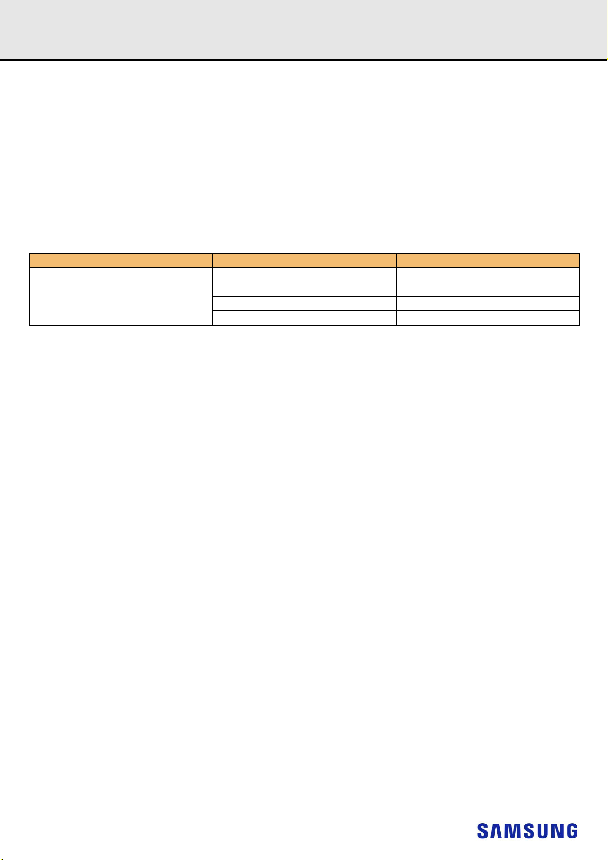
1.0 INTRODUCTION
1.1 General Description
This document describes the specification of PM961 SSD which uses PCIe interface.
The PM961 is fully consist of semiconductor device and using NAND Flash Memory which has a high reliability and a high technology in a small form fac-
tor for using a SSD and supporting Peripheral Component Interconnect Express (PCIe) 3.0 interface standard up to 4 lanes shows much faster perfor-
mance than previous SATA SSDs.
The PM961 provides 128GB, 256GB, 512GB and 1TB capacities. It’s sequential performance is up to 3000MB/s for read operation and 1700MB/s for
write operation by 4 lanes. It’s random performance is up to 360k IOPS for read and 330k IOPS for write operation by 4 lanes. It could also provide rugged
features with an extreme environment with a high MTBF.
1.2 Product List
[Table 1] Product Line-up
Typ e Capacity Part Number
128GB MZVLW128HEGR-00000/07
SAMSUNG CONFIDENTIAL
M.2
256GB MZVLW256HEHP-00000/07
512GB MZVLW512HMJP-00000/07
1TB MZVLW1T0HMLH-00000/07
1.3 Ordering Information
1. Memory (M)
2. Module Classification
Z: SSD
3. Form Factor
V: PCIeM.2 (22*80)
4. Line-Up
L: VT: Client/SV (VNAND 3bit MLC)
5. SSD CTRL
W: Polaris
6~8. SSD Density
128: 128GB
256: 256GB
512: 512GB
1T0: 1TB
9. NAND PKG + NAND Voltage
H: BGA (LF,HF)
10. Flash Generation
M: 1st Generation
E: 6th Generation
11~12. NAND Density
GR: 512G QDP 4CE
HP: 1T ODP 8CE
JP: 2T ODP 8CE
LH: 4T HDP 16CE
13. "-"
14. Default
"0"
15. HW revision
0: No revision
16. Packaging type
0: Bulk
17~18. Customer
00: General
07: General SED
IF THERE IS ANY OTHER OPERATION TO IMPLEMENT IN ADDITION TO SPECIFICATION
IN THE DATASHEET OR JEDEC STANDARD, PLEASE CONTACT EACH BRANCH OFFICE OR
HEADQUARTERS OF SAMSUNG ELECTRONICS.
- 5 -
MZVLW128HEGR-00000/07
MZVLW256HEHP-00000/07
MZVLW512HMJP-00000/07
MZVLW1T0HMLH-00000/07
datasheet SSD
2.0 PRODUCT SPECIFICATION
2.1 Capacity
[Table 2] User Addressable Sectors
Capacity Max LBA
1)
128GB
1)
256GB
1)
512GB
1TB 2,000,409,264
NOTE:
1) Gigabyte (GB) = 1,000,000,000 Bytes, 1 Sector = 512Bytes
2) Max. LBA shown in Table 1 represents the total user addressable sectors in LBA mode and calculated by IDEMA rule.
SAMSUNG CONFIDENTIAL
Rev. 1.1
250,069,680
500,118,192
1,000,215,216
2.2 Performance
[Table 3] Drive Performance
Gen3
Parameter Unit Queue Depth 128GB 256GB 512GB 1TB
Sequential Read
(Up to)
Sequential Write
(Up to)
Random Read
(Up to)
Random Write
(Up to)
NOTE:
1) Performance measured using CDM 5.0.2 on Windows 8.1 64bit. Actual performance may vary depending on use conditions and environment
2) Sequential performance measured using 128KB data size. (QD=32 by Thread=1)
3) Random performance measured using 4KB data size. (QD=32 by Thread 4, QD=1 by Thread 1)
4) Performance measurements based on TurboWrite technology
1)
2)
2)
3)
3)
MB/s QD = 32 2800 2800 2800 3000
MB/s QD = 32 600 1100 1600 1700
IOPS QD = 1 10K 10K 12K 12K
IOPS QD = 32 140K 250K 260K 360K
IOPS QD = 1 40K 50K 50K 50K
IOPS QD = 32 40K 180K 260K 330K
2.3 Power
[Table 4] Maximum Ratings
Parameter Specifications
Supply Voltage
Allowable voltage 3.3V ± 5%
Allowable noise/ripple 100mV p-p or less
[Table 5] Power Consumption for M.2 (3.3V Supply)
Parameter Specifications
Active
Power Consumption
NOTE:
1) Active power is measured on sequential write and read.
2) Idle Power is measured on Idle status with L0+APST on.
3) If L1.2 time logging option is enabled, L1.2 Power could be 5mW.
1
(Typical, RMS)
Idle
L1.2
2
(Typical)
3
(Typical)
Read 6.1W
Write 5.1W
IF THERE IS ANY OTHER OPERATION TO IMPLEMENT IN ADDITION TO SPECIFICATION
IN THE DATASHEET OR JEDEC STANDARD, PLEASE CONTACT EACH BRANCH OFFICE OR
HEADQUARTERS OF SAMSUNG ELECTRONICS.
- 6 -
450mW
5mW
MZVLW128HEGR-00000/07
SAMSUNG CONFIDENTIAL
MZVLW256HEHP-00000/07
MZVLW512HMJP-00000/07
MZVLW1T0HMLH-00000/07
datasheet SSD
2.4 Reliability
This chapter provides the information for the reliability features of the SSD.
2.4.1 MTBF
MTBF is Mean Time Between Failure, and is the predicted elapsed time between inherent failures of a system during operation. As same word,
AFR (annual failure ratio) is 0.4%. MTBF can be calculated as the arithmetic average time between failures of a system.
[Table 6] MTBF Specifications
Capacity MTBF
128GB
256GB
512GB
1TB
2.4.2 UBER
UBER is Uncorrectable Bit Error Rate.
[Table 7] UBER Specifications
Parameter Specification
UBER
1,500,000 Hours
< 1 sector per 10
15
bits read
Rev. 1.1
2.5 Environmental Specification
[Table 8] Temperature, Humidity, Shock, Vibration
Parameter Mode Specification
Temperature (Tc)
Shock
2)
3)
4)
Humidity
Vibration
NOTE:
1) Temperature is measured by SMART Temperature. Proper airflow recommended
2) Humidity is measured in non-condensing
3) Test condition for shock: 0.5ms duration with half sine wave
4) Test condition for vibration: 10Hz to 2000Hz
Operating
Non-operating -40C to 85C
Non-operating 5% to 95%
Non-operating 1500G
Non-operating 20G
1)
0C to 70C
IF THERE IS ANY OTHER OPERATION TO IMPLEMENT IN ADDITION TO SPECIFICATION
IN THE DATASHEET OR JEDEC STANDARD, PLEASE CONTACT EACH BRANCH OFFICE OR
HEADQUARTERS OF SAMSUNG ELECTRONICS.
- 7 -
MZVLW128HEGR-00000/07
MZVLW256HEHP-00000/07
MZVLW512HMJP-00000/07
MZVLW1T0HMLH-00000/07
datasheet SSD
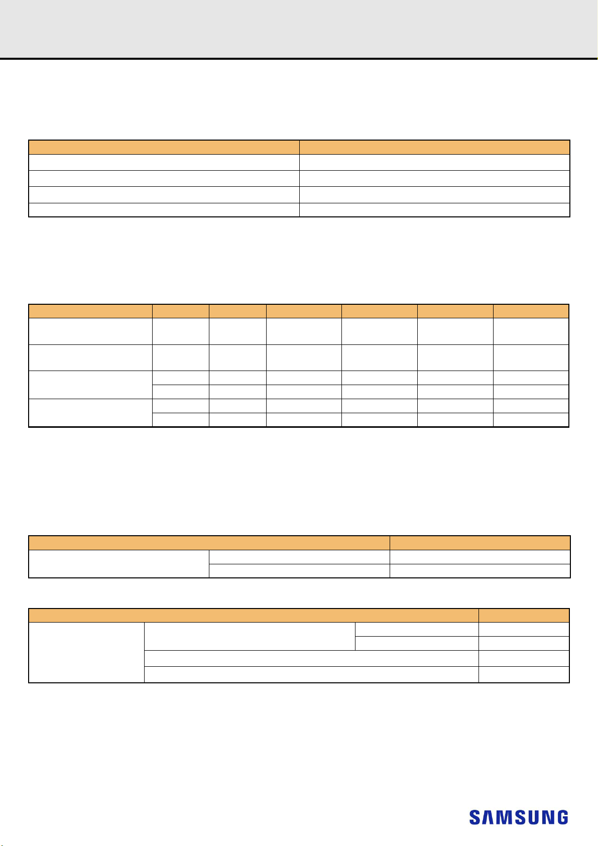
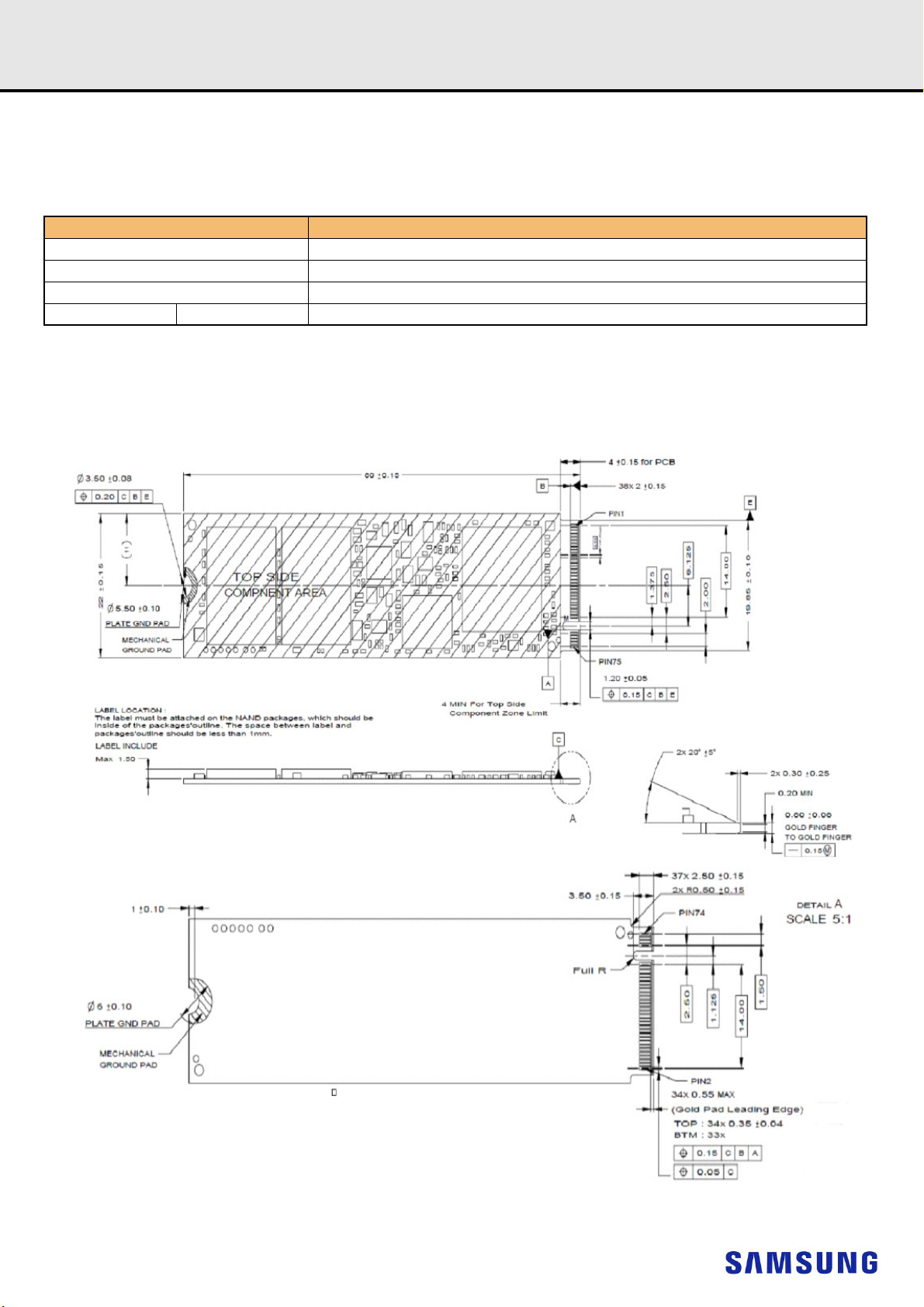
3.0 MECHANICAL SPECIFICATION
3.1 Physical dimensions and Weight
[Table 9] Physical dimensions and Weight
Parameter Value
Width 22.00 ± 0.15 mm
Length 80.00 ± 0.15 mm
Thickness Max. 2.38 mm
Weight 128/256/512GB/1TB Max 8g
3.2 Form Factor
SAMSUNG CONFIDENTIAL
Rev. 1.1
[Figure 1] M.2 Package
IF THERE IS ANY OTHER OPERATION TO IMPLEMENT IN ADDITION TO SPECIFICATION
IN THE DATASHEET OR JEDEC STANDARD, PLEASE CONTACT EACH BRANCH OFFICE OR
HEADQUARTERS OF SAMSUNG ELECTRONICS.
- 8 -
MZVLW128HEGR-00000/07
SAMSUNG CONFIDENTIAL
MZVLW256HEHP-00000/07
MZVLW512HMJP-00000/07
MZVLW1T0HMLH-00000/07
datasheet SSD
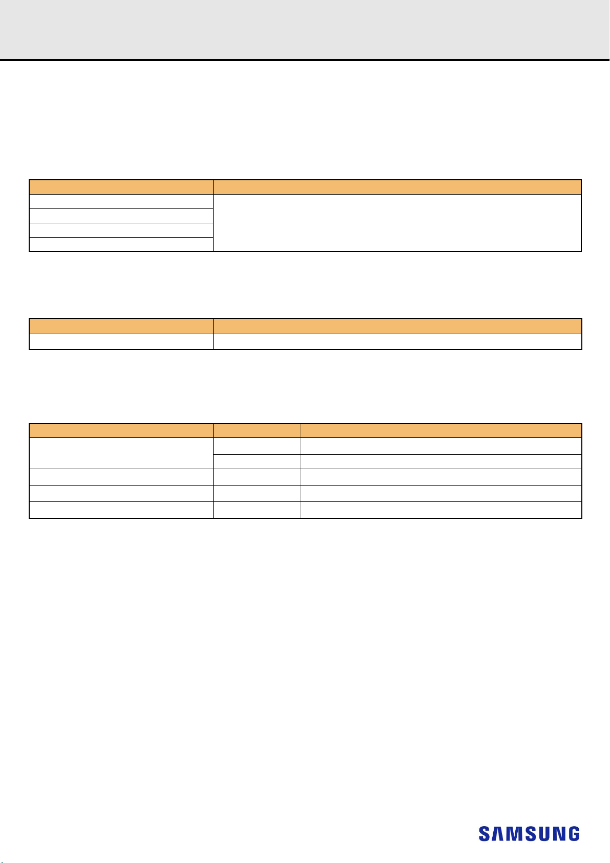
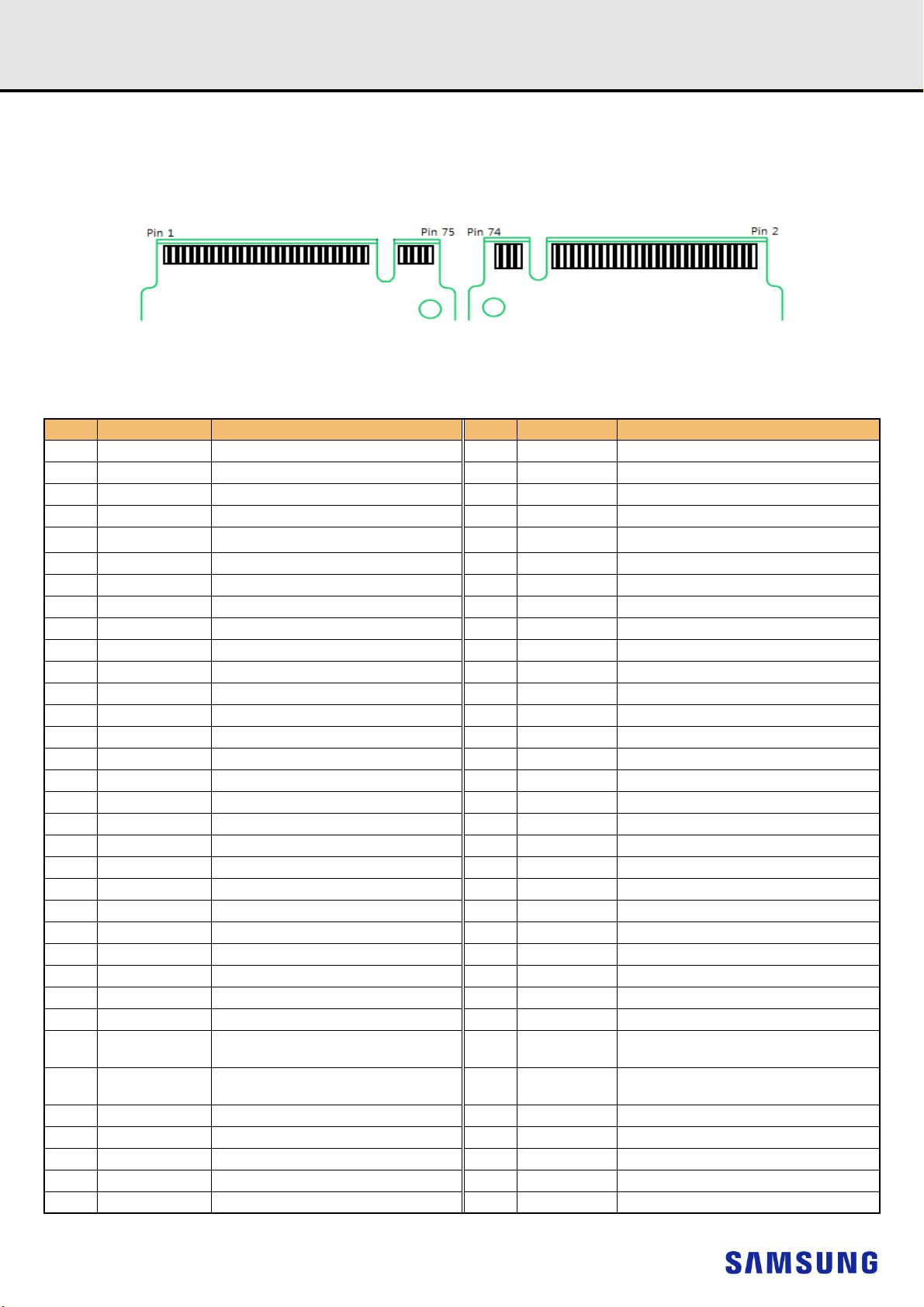
4.0 INTERFACE SPECIFACION
4.1 Connector Dimension and Pin Location
[TOP VIEW] [BOTTOM VIEW]
[Figure 2] M.2 Signal and Power pins
4.2 Pin Assignments and Definition
[Table 10] Signal Assignments
Pin# Assignment Description Pin# Assignment Description
1 GND Return current path 2 3.3V 3.3V source
3 GND Return current path 4 3.3V 3.3V source
5 PETn3 PCIe TX 6 N/C N/C
7 PETp3 PCIe TX 8 N/C N/C
9 GND Return current path 10
11 PERn3 PCIe Rx 12 3.3V 3.3V source
13 PERp3 PCIe Rx 14 3.3V 3.3V source
15 GND Return current path 16 3.3V 3.3V source
17 PETn2 PCIe TX 18 3.3V 3.3V source
19 PETp2 PCIe TX 20 N/C N/C
21 GND Return current path 22 N/C N/C
23 PERn2 PCIe Rx 24 N/C N/C
25 PERp2 PCIe Rx 26 N/C N/C
27 GND Return current path 28 N/C N/C
29 PETn1 PCIe TX 30 N/C N/C
31 PETp1 PCIe TX 32 N/C N/C
33 GND Return current path 34 N/C N/C
35 PERn1 PCIe Rx 36 N/C N/C
37 PERp1 PCIe Rx 38 N/C N/C
39 GND Return current path 40 N/C N/C
41 PETn0 PCIe TX 42 N/C N/C
43 PETp0 PCIe TX 44 N/C N/C
45 GND Return current path 46 N/C N/C
47 PERn0 PCIe Rx 48 N/C N/C
49 PERp0 PCIe Rx 50 PERST# PCIe Reset
51 GND Return current path 52 CLKREQ# PCIe Device Clock Request
53 REFCLKN PCIe Reference Clock 54 PEWake# N/C
55 REFCLKP PCIe Reference Clock 56
57 GND Return current path 58
67 N/C N/C 68 SUSCLK N/C
69 PEDET N/C 70 3.3V 3.3V source
71 GND Return current path 72 3.3V 3.3V source
73 GND Return current path 74 3.3V 3.3V source
75 GND Return current path
Reserved for
Reserved for
MFG_CLOCK
1)
LED1#
MFG_Data
IF THERE IS ANY OTHER OPERATION TO IMPLEMENT IN ADDITION TO SPECIFICATION
IN THE DATASHEET OR JEDEC STANDARD, PLEASE CONTACT EACH BRANCH OFFICE OR
HEADQUARTERS OF SAMSUNG ELECTRONICS.
- 9 -
Device Active Signal (Refer to [Table 11])
N/C
N/C
Rev. 1.1
MZVLW128HEGR-00000/07
MZVLW256HEHP-00000/07
MZVLW512HMJP-00000/07
MZVLW1T0HMLH-00000/07
[Table 11] Simple Indicator Protocol for SSD LED States (Optional)
Active State (Host send CMD to SSD) Blinking
Idle Low Power standby OFF
State Deep Sleep Power savings OFF
datasheet SSD
SAMSUNG CONFIDENTIAL
Rev. 1.1
LED Status
IF THERE IS ANY OTHER OPERATION TO IMPLEMENT IN ADDITION TO SPECIFICATION
IN THE DATASHEET OR JEDEC STANDARD, PLEASE CONTACT EACH BRANCH OFFICE OR
HEADQUARTERS OF SAMSUNG ELECTRONICS.
- 10 -
MZVLW128HEGR-00000/07
SAMSUNG CONFIDENTIAL
MZVLW256HEHP-00000/07
MZVLW512HMJP-00000/07
MZVLW1T0HMLH-00000/07
datasheet SSD
5.0 PCI and NVM Express registers
5.1 PCI Express Registers
5.1.1 PCI Register Summary
[Table 12] PCI Register Summary
Start Address End Address Name Type
00h 3Fh PCI Header PCI Capability
40h 47h PCI Power Management Capability PCI Capability
50h 67h MSI Capability PCI Capability
70h A3h PCI Express Capability PCI Capability
B0h BBh MSI-X Capability PCI Capability
100h 12Bh Advanced Error Reporting Capability PCI Capability
148h 153h Device Serial No Capability PCI Capability
158h 167h Power Budgeting Capability PCI Capability
168h 177h Secondary PCI Express Header PCI Capability
188h 18Fh Latency Tolerance Reporting (LTR) PCI Capability
190h 19Fh L1 Substates Capability Register PCI Capability
Rev. 1.1
5.1.2 PCI Header Registers
[Table 13] PCI Header Register Summary
Start Address End Address Symbol Description
00h 03h
04h 05h
06h 07h
08h 08h
09h 0Bh
0Ch 0Ch
0Dh 0Dh
0Eh 0Eh
0Fh 0Fh
10h 13h
14h 17h
18h 1Bh
1Ch 1Fh
20h 23h
24h 27h
28h 2Bh
2Ch 2Fh
30h 33h
34h 34h
35h 3Bh
3Ch 3Dh
3Eh 3Eh
3Fh 3Fh
ID Identifiers
CMD Command Register
STS Device Status
RID Revision ID
CC Class Codes
CLS Cache Line Size
MLT Master Latency Timer
HTYPE Header Type
BIST Built in Self Test
MLBAR (BAR0) Memory Register Base Address (lower 32-bit)
MUBAR (BAR1) Memory Register Base Address (upper 32-bit)
IDBAR (BAR2) Index/Data Pair Register Base Address
BAR3 Reserved
BAR4 Reserved
BAR5 Reserved
CCPTR CardBus CIS Pointer
SS Subsystem Identifiers
EROM Expansion ROM Base Address
CAP Capabilities Pointer
R Reserved
INTR Interrupt Information
MGNT Minimum Grant
MLAT Maximum Latency
IF THERE IS ANY OTHER OPERATION TO IMPLEMENT IN ADDITION TO SPECIFICATION
IN THE DATASHEET OR JEDEC STANDARD, PLEASE CONTACT EACH BRANCH OFFICE OR
HEADQUARTERS OF SAMSUNG ELECTRONICS.
- 11 -
MZVLW128HEGR-00000/07
MZVLW256HEHP-00000/07
MZVLW512HMJP-00000/07
MZVLW1T0HMLH-00000/07
[Table 14] Identifier Register
Bits Typ e Default Value Description
31:16 RO A804h Device ID
0:15 RO 144Dh Vendor ID
[Table 15] Command Register
Bits Type Default Value Description
15:11 RO 0 Reserved
10 RW 0 Interrupt Disable
9 RO 0 Fast Back-to-Back Enable (N/A)
8 RW 0 SERR# Enable (N/A)
7 RO 0 IDSEL Stepping/Wait Cycle Control (N/A)
6 RW 0 Parity Error Response Enable
5 RO 0 VGA Palette Snooping Enable (N/A)
4 RO 0 Memory Write and Invalidate Enable (N/A)
3 RO 0 Special Cycle Enable (N/A)
2 RW 0 Bus Master Enable
1 RW 0 Memory Space Enable
0 RW 0 I/O Space Enable
SAMSUNG CONFIDENTIAL
Rev. 1.1
datasheet SSD
[Table 16] Device Status Register
Bits Type Default Value Description
15 RW1C 0 Detected Parity Error
14 RW1C 0 Signaled System Error (N/A)
13 RW1C 0 Received Master Abort
12 RW1C 0 Received Target Abort
11 RW1C 0 Signaled Target Abort (N/A)
10:9 RO 0 DEVSEL Timing (N/A)
8 RW1C 0 Master Data Parity Error Detected
7 RO 0 Fast Back-to-Back Transaction Capable (N/A)
6RO 0 Reserved
5 RO 0 66MHz Capable (N/A)
4 RO 1 Capabilities List
3 RO 0 INTx Status
2:0 RO 0 Reserved
[Table 17] Revision ID Register
Bits Ty pe Default Value Description
7:0 RO 00h Controller Hardware Revision ID
[Table 18] Class Code Register
Bits Type Default Value Description
23:16 RO 1h Base Class Code
15:8 RO 8h Sub Class Code
7:0 RO 2h Programming Interface
IF THERE IS ANY OTHER OPERATION TO IMPLEMENT IN ADDITION TO SPECIFICATION
IN THE DATASHEET OR JEDEC STANDARD, PLEASE CONTACT EACH BRANCH OFFICE OR
HEADQUARTERS OF SAMSUNG ELECTRONICS.
- 12 -
MZVLW128HEGR-00000/07
MZVLW256HEHP-00000/07
MZVLW512HMJP-00000/07
MZVLW1T0HMLH-00000/07
[Table 19] Cache Line Size Register
Bits Typ e Default Value Description
7:0 RW 0h N/A
[Table 20] Master Latency Timer Register
Bits Ty pe Default Value Description
7:0 RO 0 N/A
[Table 21] Header Type Register
Bits Ty pe Default Value Description
7:0 RO 0 N/A
[Table 22] Built In Self Test Register
Bits Typ e Default Value Description
7:0 RO 0 N/A
SAMSUNG CONFIDENTIAL
Rev. 1.1
datasheet SSD
[Table 23] Memory Register Base Address Lower 32-bits (BAR0) Register
Bits Type Default Value Description
31:14 RW 0
13:4 RO 0
2:1 RO 2 Address Type (64-bit)
0 RO 0 Memory Space Indicator (MEMSI)
[Table 24] Memory Register Base Address Upper 32-bits (BAR1)
Bits Ty pe Default Value Description
31:0 RO 0 Base Address
[Table 25] Index/Data Pair Register Base Address (BAR2) Register
Bits Ty pe Default Value Description
31:0 RO 0 N/A
[Table 26] BAR3 Register
Bits Ty pe Default Value Description
31:0 RO 0 N/A
[Table 27] Vendor Specific BAR4 Register
Bits Type Default Value Description
31:0 RO 0 N/A
Base Address
[Table 28] Vendor Specific BAR5 Register
Bits Type Default Value Description
31:0 RO 0 N/A
[Table 29] Cardbus CIS Pointer Register
Bits Type Default Value Description
31:0 RO 0 N/A
IF THERE IS ANY OTHER OPERATION TO IMPLEMENT IN ADDITION TO SPECIFICATION
IN THE DATASHEET OR JEDEC STANDARD, PLEASE CONTACT EACH BRANCH OFFICE OR
HEADQUARTERS OF SAMSUNG ELECTRONICS.
- 13 -
 Loading...