


SAMSUNG CONFIDENTIAL
Rev. 1.1 Sep. 2017
MZVLB256HAHQ-00000/07
MZVLB512HAJQ-00000/07
MZVLB1T0HALR-00000/07
MZVLB2T0HMLB-00000/07
M.2 NVMe PCIe SSD
specification
(PM981)
datasheet
SAMSUNG ELECTRONICS RESERVES THE RIGHT TO CHANGE PRODUCTS, INFORMATION AND
SPECIFICATIONS WITHOUT NOTICE.
Products and specifications discussed herein are for reference purposes only. All information discussed
herein is provided on an "AS IS" basis, without warranties of any kind.
This document and all information discussed herein remain the sole and exclusive property of Samsung
Electronics. No license of any patent, copyright, mask work, trademark or any other intellectual property
right is granted by one party to the other party under this document, by implication, estoppel or otherwise.
Samsung products are not intended for use in life support, critical care, medical, safety equipment, or
similar applications where product failure could result in loss of life or personal or physical harm, or any
military or defense application, or any governmental procurement to which special terms or provisions
may apply.
For updates or additional information about Samsung products, contact your nearest Samsung office.
All brand names, trademarks and registered trademarks belong to their respective owners.
ⓒ 2017 Samsung Electronics Co., Ltd. All rights reserved.
- 1 -
MZVLB256HAHQ-00000/07
MZVLB512HAJQ-00000/07
MZVLB1T0HALR-00000/07
MZVLB2T0HMLB-00000/07
datasheet
SAMSUNG CONFIDENTIAL
Rev. 1.1
SSD
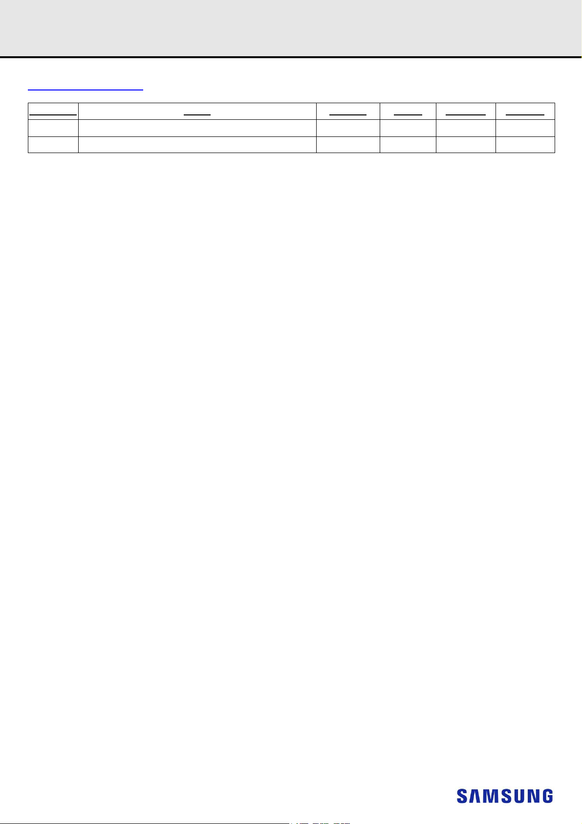
Revision History
Revision No. History Draft Date Remark Created by Review by
1.0 1. Initial issue Aug 07, 2017 Final K.W Shin
1.1 1.Deleted 128GB and changed the part number of 256GB. Sep. 28, 2017 Final S.J Oh Elly. Shin
IF THERE IS ANY OTHER OPERATION TO IMPLEMENT IN ADDITION TO SPECIFICATION
IN THE DATASHEET OR JEDEC STANDARD, PLEASE CONTACT EACH BRANCH OFFICE OR
HEADQUARTERS OF SAMSUNG ELECTRONICS.
- 2 -

MZVLB256HAHQ-00000/07
MZVLB512HAJQ-00000/07
MZVLB1T0HALR-00000/07
MZVLB2T0HMLB-00000/07
datasheet
SAMSUNG CONFIDENTIAL
Rev. 1.1
SSD
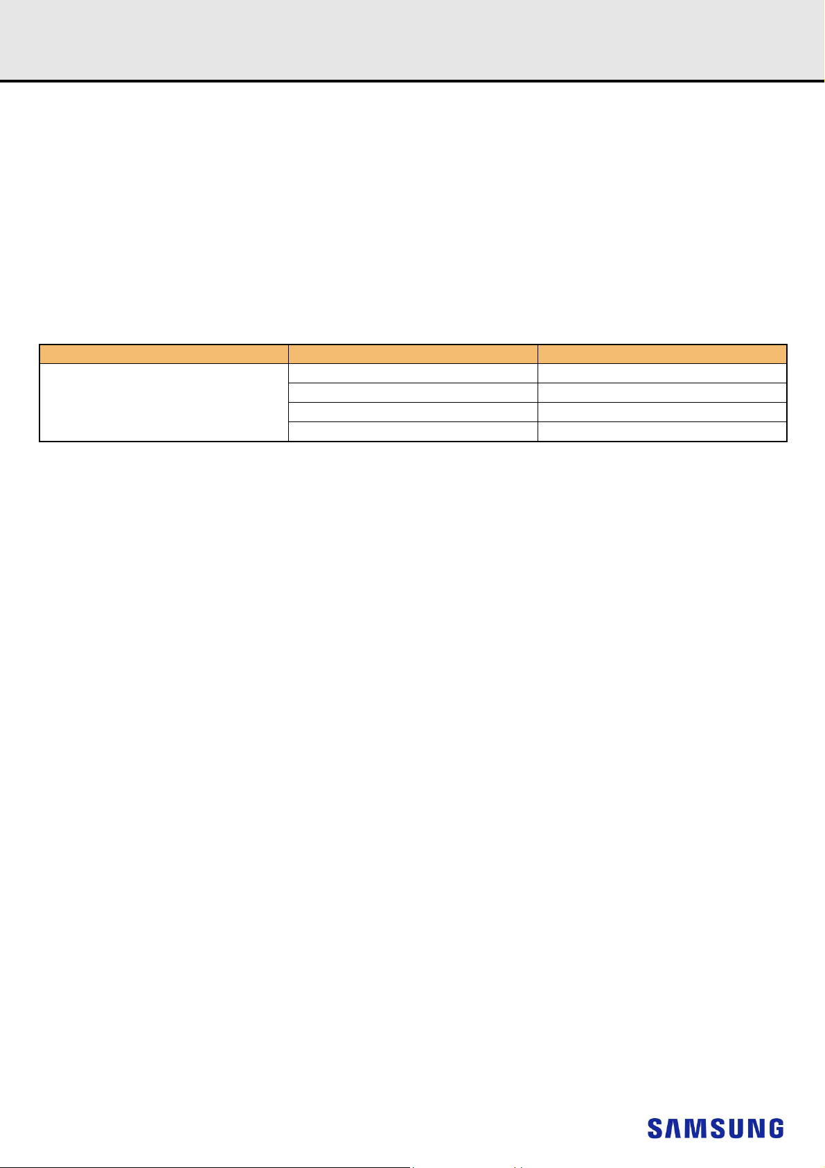
PM981 Series
PART NUMBER
MZVLB256HAHQ-00000/07 256GB 500,118,192
MZVLB512HAJQ-00000/07 512GB 1,000,215,216
MZVLB1T0HALR-00000/07 1TB 2,000,409,264
MZVLB2T0HMLB-00000/07 2TB 4,000,797,360
FEATURES Environmental Specifications
PCIe Gen3 8Gb/s Interface, up to 4 Lanes
Compliant with PCI Express Base Specification Rev. 3.0
Compliant with PCI Express M.2 Specification Rev. 1.1
Compliant with NVMe Express specification Rev. 1.2a
Power Saving Modes:
- Supporting APST Linear Shock (0.5ms duration with 1/2 sine wave)
- Supporting L1.2 Mode Non-operating 1,500 Gpeak
Support Admin & NVM Command Set
RoHS Compliant
Hardware based AES-XTS 256-bit Encryption Engine for SED
TCG OPAL (v2.0) Compliant for SED
Drive Configuration
Capacity 256/512GB/1/2TB
From Factor M.2 - Read 5.9W
Interface PCI Express Gen3 x4 - Write 5.7W
Bytes per Sector 512Byte
Performance Specifications
Data Transfer Rate (128KB)
3)
Capacity
1)
Temperature
5
(Typ, RMS)
(Typ.)
4
7
Operating
Non-operating
Humidity (non-condensing)
Non-operating 5 ~ 95%
Vibration
Non-operating (20 ~ 2,000 Hz, Sinusoidal) 20 Gpeak
POWER SPECIFICATIONS
Supply Voltage / Tolerance 3.3V ± 5%
Voltage Ripple/Noise (max.) 100mV p-p
Active
6
Idle
L1.2 (Typ) 5mW
PHYSICAL DIMENSION
LBA
2)
0°C to 70°C
-40
°
C to 85°C
30mW
Sequential Read (1TB) Up to 3,200 MB/s Width 22.00 ± 0.15 mm
(512GB) Up to 3,000 MB/s Length 80.00 ± 0.15 mm
(256GB/2TB) Up to TBD MB/s Height
Sequential Write (1TB) Up to 2,400 MB/s - Single Side Max. 2.38 mm
(512GB) Up to 1,800 MB/s Weight Max. 9.0g
(256GB/2TB) Up to TBD MB/s
Data I/O Speed (4KB)
Random Read (1TB) Up to 380K IOPS
(512GB) Up to 270K IOPS
(256GB/2TB) Up to TBD IOPS
Random Write (1TB) Up to 440K IOPS
(512GB) Up to 420K IOPS
(256GB/2TB) Up to TBD IOPS
Reliability Specifications
UBER
MTBF 1.5 Million Hours
< 1 sector per 10
15
bits read
Specifications are subject to change without notice.
1) 1MB = 1,000,000 Bytes, 1GB = 1,000,000,000 Bytes, Unformatted Capacity.
User accessible capacity may vary depending on operating environment and
formatting.
2) 1 Sector = 512Bytes, Max. LBA represents the total user addressable sectors
in LBA mode and calculated by IDEMA rule
3) Actual performance may vary depending on use conditions and environment. Performance measurements based on TurboWri te technology.
4) Measured by SMART Temperature. Proper airflow recommended.
5) Active power is measured on sequential write and read.
6) Idle Power is measured on Idle status with L1.2+APST/ASPM on.
7) Active/Idle/L1.2 Power are measured up to 1TB.
IF THERE IS ANY OTHER OPERATION TO IMPLEMENT IN ADDITION TO SPECIFICATION
IN THE DATASHEET OR JEDEC STANDARD, PLEASE CONTACT EACH BRANCH OFFICE OR
HEADQUARTERS OF SAMSUNG ELECTRONICS.
- 3 -

MZVLB256HAHQ-00000/07
SAMSUNG CONFIDENTIAL
MZVLB512HAJQ-00000/07
MZVLB1T0HALR-00000/07
MZVLB2T0HMLB-00000/07
datasheet
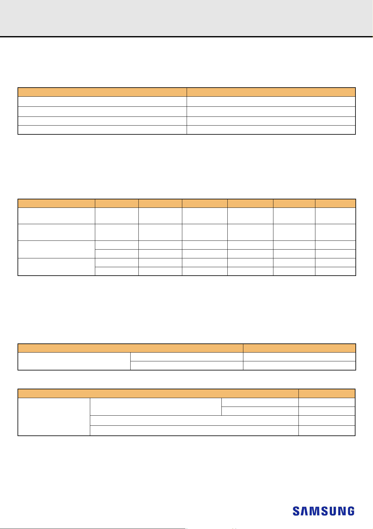
Table Of Contents
1.0 INTRODUCTION ........................................................................................................................................................5
1.1 General Description................................................................................................................................................5
1.2 Product List..............................................................................................................................................................5
1.3 Ordering Information................................................................................................................................................5
2.0 PRODUCT SPECIFICATION......................................................................................................................................6
2.1 Capacity...................................................................................................................................................................6
2.2 Performance
2.3 Power ......................................................................................................................................................................6
2.4 Reliability.................................................................................................................................................................7
2.4.1 MTBF ....................................... .........................................................................................................................7
2.4.2 UBER................................................................................................................................................................7
2.5 Environmental Specification....................................................................................................................................7
3.0 MECHANICAL SPECIFICATION.............. ... ............................................................................ ..................................8
3.1 Physical dimensions and Weight.............................................................................................................................8
3.2 Form Factor.............................................................................................................................................................8
4.0 INTERFACE SPECIFACION......................................................................................................................................9
4.1 Connector Dimension and Pin Location..................................................................................................................9
4.2 Pin Assignments and Definition...............................................................................................................................9
5.0 PCI and NVM Express registers.................................................................................................................................11
5.1 PCI Express Registers ............................................................................................................................................11
5.1.1 PCI Register Summary .....................................................................................................................................11
5.1.2 PCI Configuration Header Space Registers Detail ...........................................................................................11
5.1.2.1 PCI Configuration Header Space Registers ...............................................................................................11
5.1.3 PCI Capability Registers Detail.........................................................................................................................14
5.1.3.1 PCI Power Management Capability............................................................................................................14
5.1.3.2 Message Signaled Interrupt (MSI) Capability...................................................................... ... ....................15
5.1.3.3 PCI Express Capability.......................................... .....................................................................................17
5.1.3.4 MSI-X Capability...................................... ........................................ ...........................................................21
5.1.4 PCI Extended Capability Details .......................................................................................................................22
5.1.4.1 Advanced Error Reporting Registers..........................................................................................................22
5.1.4.2 Device Serial Number Capability................................................................................................................25
5.1.4.3 Power Budgeting Capability........................................................................................................................26
5.1.4.4 Secondary PCI Express Capability.............................................................................................................27
5.1.4.5 Latency Tolerance Reporting Capability Registers.......................................................................
5.1.4.6 L1 Substates Extended Capability..............................................................................................................29
5.2 NVM Express Registers ..........................................................................................................................................30
5.2.1 Register Summary .................................... .................................... ....................................................................30
5.2.2 Controller Registers ....................................... ... ... .................................... ... ......................................................30
6.0 Supported Command Set ...........................................................................................................................................34
6.1 Admin Command Set ..............................................................................................................................................34
6.1.1 Identify Command............................... ..................................... .. .......................................................................35
6.2 NVM Express I/O Command Set.............................................................................................................................41
6.3 SMART/Health Information......................................................................................................................................42
7.0 PRODUCT COMPLIANCE .........................................................................................................................................43
7.1 Product regulatory compliance and Certifications ...................................................................................................43
8.0 References..................................................................................................................................................................44
1)
..........................................................................................................................................................6
..............28
Rev. 1.1
SSD
IF THERE IS ANY OTHER OPERATION TO IMPLEMENT IN ADDITION TO SPECIFICATION
IN THE DATASHEET OR JEDEC STANDARD, PLEASE CONTACT EACH BRANCH OFFICE OR
HEADQUARTERS OF SAMSUNG ELECTRONICS.
- 4 -
MZVLB256HAHQ-00000/07
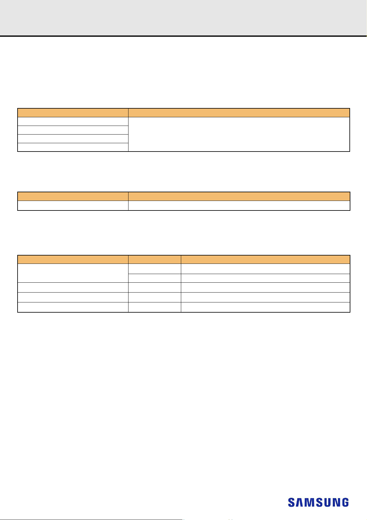
M Z X X X X X X X X X X - X X X X X
1 2 3 4 5 6 7 8 9 10 11 12 13 14 15 16 17 18
MZVLB512HAJQ-00000/07
MZVLB1T0HALR-00000/07
MZVLB2T0HMLB-00000/07
datasheet
SAMSUNG CONFIDENTIAL
Rev. 1.1
SSD
1.0 INTRODUCTION
1.1 General Description
This document describes the specification of PM981 SSD which uses PCIe interface.
The PM981 is fully consist of semiconductor device and using NAND Flash Memory which has a high reliability and a high technology in a small form factor for using a SSD and supporting Peripheral Component Interconnect Express (PCIe) 3.0 interface standard up to 4 lanes shows much faster performance than previous SATA SSDs.
The PM981 provides 256GB, 512GB, 1TB and 2TB capacities. It’s sequential performance is up to 3,200MB/s for read operation and 2,400MB/s for write
operation by 4 lanes. It’s random performance is up to 380k IOPS for read and 440k IOPS for write operation by 4 lanes. It could also provide rugged features with an extreme environment with a high MTBF.
1.2 Product List
[Table 1] Product Line-up
Type Capacity Part Number
256GB MZVLB256HAHQ-00000/07
M.2
512GB MZVLB512HAJQ-00000/07
1TB MZVLB1T0HALR-00000/07
2TB MZVLB2T0HMLB-00000/07
1.3 Ordering Information
1. Memory (M)
2. Module Classification
Z: SSD
3. Form Factor
V: PCIeM.2 (22*80, PCIe x4)
4. Line-Up
L: Client/SV (VNAND 3bit MLC)
5. SSD CTRL
B: Phoenix
6~8. SSD Density
256: 256GB
512: 512GB
1T0: 1TB
2T0: 2TB
9. NAND PKG + NAND Voltage
H: BGA (LF,HF)
10. Flash Generation
M: 1st Generation
A: 2nd Generation
11~12. NAND Density
HQ: 1T QDP 4CE
JQ: 2T ODP 4CE
LR: 4T HDP 4CE
LB: 8T HDP 4CE
13. "-"
14. Default
"0"
15. HW revision
0: No revision
16. Packaging type
0: Bulk
17~18. Customer
00: World wide (non-SED)
07: World wide (SED)
IF THERE IS ANY OTHER OPERATION TO IMPLEMENT IN ADDITION TO SPECIFICATION
IN THE DATASHEET OR JEDEC STANDARD, PLEASE CONTACT EACH BRANCH OFFICE OR
HEADQUARTERS OF SAMSUNG ELECTRONICS.
- 5 -
MZVLB256HAHQ-00000/07
MZVLB512HAJQ-00000/07
MZVLB1T0HALR-00000/07
MZVLB2T0HMLB-00000/07
datasheet
2.0 PRODUCT SPECIFICATION
2.1 Capacity
[Table 2] User Addressable Sectors
Capacity Max LBA
1)
256GB
1)
512GB
1TB 2,000,409,264
2TB 4,000,797,360
NOTE:
1) Gigabyte (GB) = 1,000,000,000 Bytes, 1 Sector = 512Bytes
2) Max. LBA shown in Table 1 represents the total user addressable sectors in LBA mode and calculated by IDEMA rule.
SAMSUNG CONFIDENTIAL
Rev. 1.1
SSD
500,118,192
1,000,215,216
2.2 Performance
[Table 3] Drive Performance
Gen3
Parameter Unit Queue Depth 256GB 512GB 1TB 2TB
Sequential Read
(Up to)
Sequential Write
(Up to)
Random Read
(Up to)
Random Write
(Up to)
NOTE:
1) Performance measured using CDM 5.0.2 on Windows 10 64bit. Actual performance may vary depending on use conditions and en vironment.
2) Sequential performance measured using 128KB data size. (QD=32 by Thread=1)
3) Random performance measured using 4KB data size. (QD=32 by Thread 4, QD=1 by Thread 1)
4) Performance measurements based on TurboWrite technology
1)
2)
2)
3)
3)
MB/s QD = 32 TBD 3,000 3,200 TBD
MB/s QD = 32 TBD 1,800 2,400 TBD
IOPS QD = 1 TBD 12K 12K TBD
IOPS QD = 32 TBD 270K 380K TBD
IOPS QD = 1 TBD 50K 50K TBD
IOPS QD = 32 TBD 420K 440K TBD
2.3 Power
[Table 4] Maximum Ratings
Parameter Specifications
Supply Voltage
Allowable voltage 3.3V ± 5%
Allowable noise/ripple 100mV p-p or less
[Table 5] Power Consumption for M.2 (3.3V Supply)
Parameter Specifications
Active1 (Typical, RMS)
Power Consumption
NOTE:
1) Active power is measured on sequential write and read.
2) Idle Power is measured on Idle status with L1.2+APST/ASPM on.
3) If L1.2 time logging option is enabled, L1.2 Power could be 5mW.
4) Active/Idle/L1.2 Power are measured up to 1TB.
4
Idle
L1.2
2
(Typical)
3
(Typical)
Read 5.9W
Write 5.7W
IF THERE IS ANY OTHER OPERATION TO IMPLEMENT IN ADDITION TO SPECIFICATION
IN THE DATASHEET OR JEDEC STANDARD, PLEASE CONTACT EACH BRANCH OFFICE OR
HEADQUARTERS OF SAMSUNG ELECTRONICS.
- 6 -
30mW
5mW
MZVLB256HAHQ-00000/07
SAMSUNG CONFIDENTIAL
MZVLB512HAJQ-00000/07
MZVLB1T0HALR-00000/07
MZVLB2T0HMLB-00000/07
datasheet
2.4 Reliability
This chapter provides the information for the reliability features of the SSD.
2.4.1 MTBF
MTBF is Mean Time Between Failure, and is the predicted elapsed time between inherent failures of a system during operation. As same word,
AFR (annual failure ratio) is 0.4%. MTBF can be calculated as the arithmetic average time between failures of a system.
[Table 6] MTBF Specifications
Capacity MTBF
256GB
512GB
1TB
2TB
2.4.2 UBER
UBER is Uncorrectable Bit Error Rate.
[Table 7] UBER Specifications
Parameter Specification
UBER
1,500,000 Hours
< 1 sector per 10
15
bits read
Rev. 1.1
SSD
2.5 Environmental Specification
[Table 8] Temperature, Humidity, Shock, Vibration
Parameter Mode Specification
Temperature
Shock
2)
3)
4)
Humidity
Vibration
NOTE:
1) Temperature is measured by SMART Temperature. Proper airflow recommended
2) Humidity is measured in non-condensing
3) Test condition for shock: 0.5ms duration with half sine wave
4) Test condition for vibration: 10Hz to 2000Hz
Operating
Non-operating -40C to 85C
Non-operating 5% to 95%
Non-operating 1500G
Non-operating 20G
1)
0C to 70C
IF THERE IS ANY OTHER OPERATION TO IMPLEMENT IN ADDITION TO SPECIFICATION
IN THE DATASHEET OR JEDEC STANDARD, PLEASE CONTACT EACH BRANCH OFFICE OR
HEADQUARTERS OF SAMSUNG ELECTRONICS.
- 7 -
MZVLB256HAHQ-00000/07
MZVLB512HAJQ-00000/07
MZVLB1T0HALR-00000/07
MZVLB2T0HMLB-00000/07
datasheet
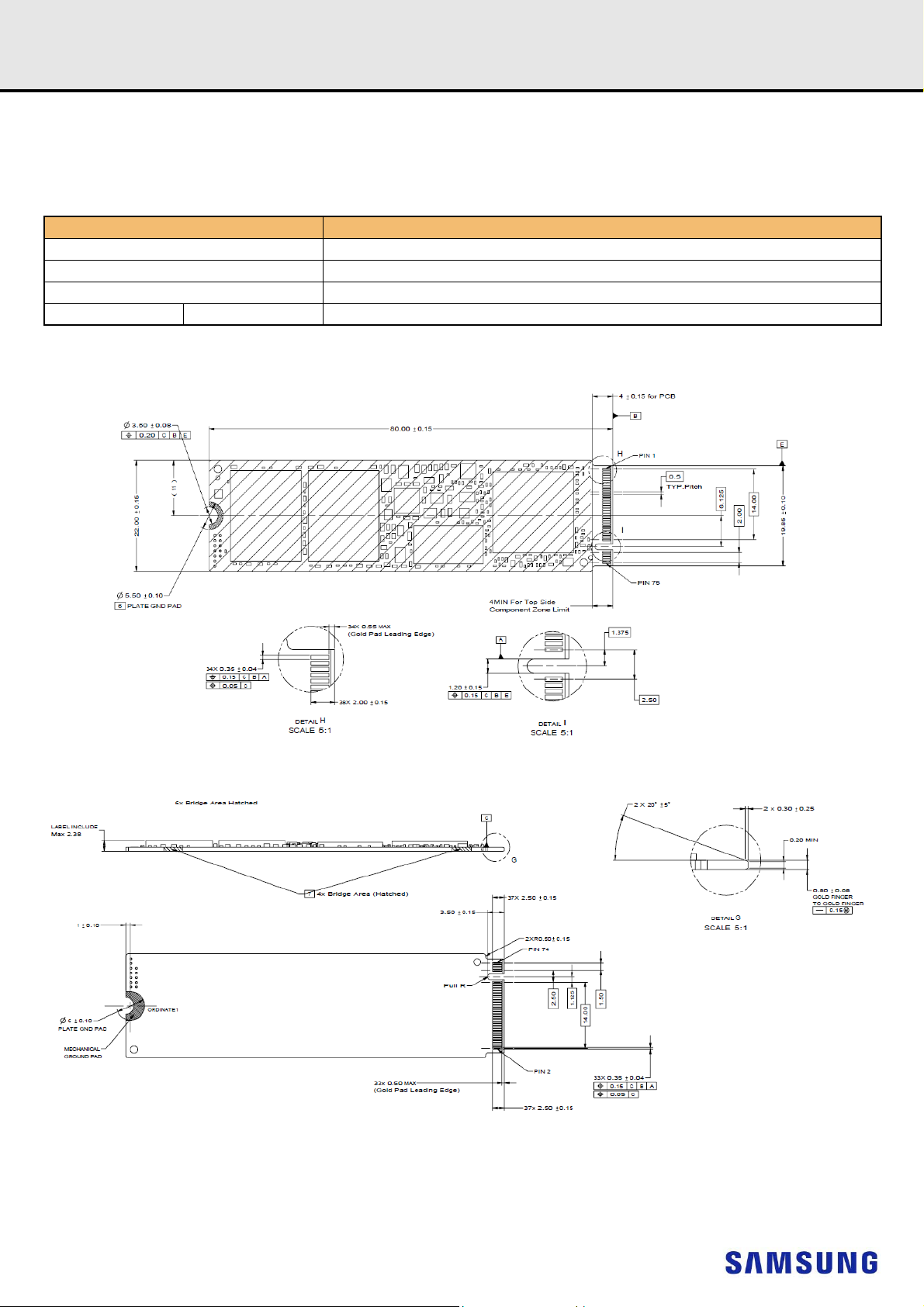
3.0 MECHANICAL SPECIFICATION
3.1 Physical dimensions and Weight
[Table 9] Physical dimensions and Weight
Parameter Value
Width 22.00 ± 0.15 mm
Length 80.00 ± 0.15 mm
Thickness Max. 2.38 mm
Weight 256/512GB/1/2TB Max 9.0g
3.2 Form Factor
SAMSUNG CONFIDENTIAL
Rev. 1.1
SSD
[Figure 1] M.2 Package
IF THERE IS ANY OTHER OPERATION TO IMPLEMENT IN ADDITION TO SPECIFICATION
IN THE DATASHEET OR JEDEC STANDARD, PLEASE CONTACT EACH BRANCH OFFICE OR
HEADQUARTERS OF SAMSUNG ELECTRONICS.
- 8 -
MZVLB256HAHQ-00000/07
SAMSUNG CONFIDENTIAL
MZVLB512HAJQ-00000/07
MZVLB1T0HALR-00000/07
MZVLB2T0HMLB-00000/07
datasheet
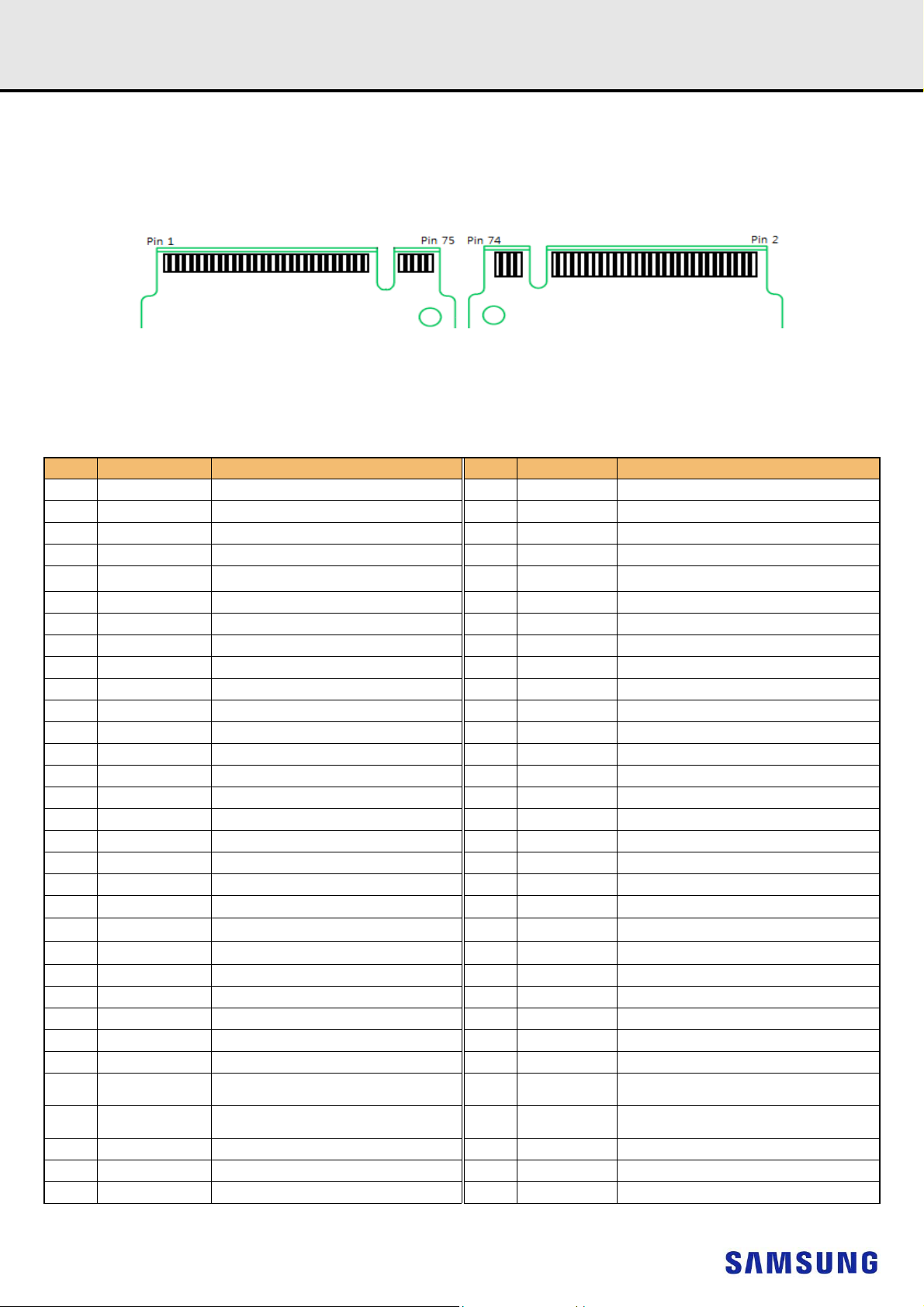
4.0 INTERFACE SPECIFACION
4.1 Connector Dimension and Pin Location
[TOP VIEW] [BOTTOM VIEW]
[Figure 2] M.2 Signal and Power pins
4.2 Pin Assignments and Definition
[Table 10] Signal Assignments
Pin# Assignment Description Pin# Assignment Description
1 GND Return current path 2 3.3V 3.3V source
3 GND Return current path 4 3.3V 3.3V source
5 PETn3 PCIe TX 6 N/C N/C
7 PETp3 PCIe TX 8 N/C N/C
9 GND Return current path 10
11 PERn3 PCIe Rx 12 3.3V 3.3V source
13 PERp3 PCIe Rx 14 3.3V 3.3V source
15 GND Return current path 16 3.3V 3.3V source
17 PETn2 PCIe TX 18 3.3V 3.3V source
19 PETp2 PCIe TX 20 N/C N/C
21 GND Return current path 22 N/C N/C
23 PERn2 PCIe Rx 24 N/C N/C
25 PERp2 PCIe Rx 26 N/C N/C
27 GND Return current path 28 N/C N/C
29 PETn1 PCIe TX 30 N/C N/C
31 PETp1 PCIe TX 32 N/C N/C
33 GND Return current path 34 N/C N/C
35 PERn1 PCIe Rx 36 N/C N/C
37 PERp1 PCIe Rx 38 N/C N/C
39 GND Return current path 40
41 PETn0 PCIe TX 42
43 PETp0 PCIe TX 44
45 GND Return current path 46 N/C N/C
47 PERn0 PCIe Rx 48 N/C N/C
49 PERp0 PCIe Rx 50 PERST# PCIe Reset
51 GND Return current path 52 CLKREQ# PCIe Device Clock Request
53 REFCLKN PCIe Reference Clock 54 PEWake# N/C
55 REFCLKP PCIe Reference Clock 56
57 GND Return current path 58
67 N/C N/C 68 SUSCLK DNU (Do Not Use)
69 PEDET N/C 70 3.3V 3.3V source
71 GND Return current path 72 3.3V 3.3V source
LED1#
ALTER#(O)
SMB_DATA (I/O)
SMB_CLK (I/O)
Reserved for
MFG_Data
Reserved for
MFG_CLOCK
Device Active Signal (Refer to [Table 11])
1)
2)
2)
DNU (Do Not Use)
DNU (Do Not Use)
DNU (Do Not Use)
N/C
N/C
Rev. 1.1
SSD
IF THERE IS ANY OTHER OPERATION TO IMPLEMENT IN ADDITION TO SPECIFICATION
IN THE DATASHEET OR JEDEC STANDARD, PLEASE CONTACT EACH BRANCH OFFICE OR
HEADQUARTERS OF SAMSUNG ELECTRONICS.
- 9 -

MZVLB256HAHQ-00000/07
SAMSUNG CONFIDENTIAL
MZVLB512HAJQ-00000/07
MZVLB1T0HALR-00000/07
MZVLB2T0HMLB-00000/07
73 GND Return current path 74 3.3V 3.3V source
75 GND Return current path
NOTE:
1) Not support: open drain with pull-up on platform (1.8V), active low.
2) Not support: open drain with pull-up on platform (1.8V).
[Table 11] Simple Indicator Protocol for SSD LED States (Optional)
Active State (Host send CMD to SSD) Blinking
Idle Low Power standby OFF
State Deep Sleep Power savings OFF
NOTE:
1) ASPM (Active State Power Management)
datasheet
1)
ASPM
Rev. 1.1
SSD
LED Status
IF THERE IS ANY OTHER OPERATION TO IMPLEMENT IN ADDITION TO SPECIFICATION
IN THE DATASHEET OR JEDEC STANDARD, PLEASE CONTACT EACH BRANCH OFFICE OR
HEADQUARTERS OF SAMSUNG ELECTRONICS.
- 10 -
MZVLB256HAHQ-00000/07
MZVLB512HAJQ-00000/07
MZVLB1T0HALR-00000/07
MZVLB2T0HMLB-00000/07
datasheet
5.0 PCI and NVM Express registers
5.1 PCI Express Registers
5.1.1 PCI Register Summary
[Table 12] PCI Register Summary
Start Address End Address Name Type
00h 3Fh PCI Header PCI Configuration Header Space
40h 47h PCI Power Management Capability PCI Capability
50h 67h MSI Capability PCI Capability
70h A3h PCI Express Capability PCI Capability
B0h BBh MSI-X Capability PCI Capability
100h 12Bh Advanced Error Reporting Capability PCI Extended Capability
148h 153h Device Serial Number Capability PCI Extended Capability
158h 167h Power Budgeting Capability PCI Extended Capability
168h 17Bh Secondary PCI Express Capability PCI Extended Capability
188h 18Fh Latency Tolerance Reporting Capability PCI Extended Capability
190h 19Fh L1 Substates Capability PCI Extended Capability
SAMSUNG CONFIDENTIAL
Rev. 1.1
SSD
5.1.2 PCI Configuration Header Space Registers Detail
5.1.2.1 PCI Configuration Header Space Registers
[Table 13] PCI Header Space Summary
Start Address End Address Symbol Description
00h 03h
04h 05h
06h 07h
08h 08h
09h 0Bh
0Ch 0Ch
0Dh 0Dh
0Eh 0Eh
0Fh 0Fh
10h 13h
14h 17h
18h 1Bh
1Ch 1Fh
20h 23h
24h 27h
28h 2Bh
2Ch 2Fh
30h 33h
34h 34h
35h 3Bh
3Ch 3Dh
3Eh 3Eh
3Fh 3Fh
IDTF Identifiers
CMD Command Register
STS Status Register
REVID Revision ID
CC Class Codes
CLS Cache Line Size
MLT Master Latency Timer
HTYPE Header Type
BIST Built in Self Test
MLBAR (BAR0) Memory Register Base Address (lower 32-bit)
MUBAR (BAR1) Memory Register Base Address (upper 32-bit)
IDBAR (BAR2) Reserved
BAR3 Reserved
BAR4 Reserved
BAR5 Reserved
CCPTR CardBus CIS Pointer
SS Subsystem Identifiers
EXPROM Expansion ROM Base Address
CAP Capabilities Pointer
R Reserved
INTR Interrupt Information
MGNT Minimum Grant
MLAT Maximum Latency
IF THERE IS ANY OTHER OPERATION TO IMPLEMENT IN ADDITION TO SPECIFICATION
IN THE DATASHEET OR JEDEC STANDARD, PLEASE CONTACT EACH BRANCH OFFICE OR
HEADQUARTERS OF SAMSUNG ELECTRONICS.
- 11 -
MZVLB256HAHQ-00000/07
MZVLB512HAJQ-00000/07
MZVLB1T0HALR-00000/07
MZVLB2T0HMLB-00000/07
[Table 14] Identifier Register
Bits Type Default Value Description
31:16 RO A808h Device ID
0:15 RO 144Dh Vendor ID
[Table 15] Command Register
Bits Type Default Value Description
15:11 RO 0h Reserved
10 RW 0 Interrupt Disable
9 RO 0 Fast Back-to-Back Enable (N/A)
8 RW 0 SERR# Enable
7 RO 0 IDSEL Stepping/Wait Cycle Control (N/A)
6 RW 0 Parity Error Response Enable
5 RO 0 VGA Palette Snooping Enable (N/A)
4 RO 0 Memory Write and Invalidate Enable (N/A)
3 RO 0 Special Cycle Enable (N/A)
2 RW 0 Bus Master Enable
1 RW 0 Memory Space Enable
0 RW 0 I/O Space Enable
datasheet
SAMSUNG CONFIDENTIAL
Rev. 1.1
SSD
[Table 16] Status Register
Bits Type Default Value Description
15 RW1C 0 Detected Parity Error
14 RW1C 0 Signaled System Error
13 RW1C 0 Received Master Abort
12 RW1C 0 Received Target Abort
11 RW1C 0 Signaled Target Abort (N/A)
10:9 RO 0h DEVSEL Timing (N/A)
8 RW1C 0 Master Data Parity Error Detected
7 RO 0 Fast Back-to-Back Transaction Capable (N/A)
6RO 0 Reserved
5 RO 0 66MHz Capable (N/A)
4 RO 1 Capabilities List
3 RO 0 Interrupt Status
2:1 RO 0h Reserved
0RO 0 Reserved
[Table 17] Revision ID Register
Bits Type Default Value Description
7:0 RO 00h Controller Hardware Revision ID
[Table 18] Class Code Register
Bits Type Default Value Description
23:16 RO 1h Base Class Code
15:8 RO 8h Sub Class Code
7:0 RO 2h Programming Interface
IF THERE IS ANY OTHER OPERATION TO IMPLEMENT IN ADDITION TO SPECIFICATION
IN THE DATASHEET OR JEDEC STANDARD, PLEASE CONTACT EACH BRANCH OFFICE OR
HEADQUARTERS OF SAMSUNG ELECTRONICS.
- 12 -
MZVLB256HAHQ-00000/07
MZVLB512HAJQ-00000/07
MZVLB1T0HALR-00000/07
MZVLB2T0HMLB-00000/07
[Table 19] Cache Line Size Register
Bits Type Default Value Description
7:0 RW 0h Cache Line Size (N/A)
[Table 20] Master Latency Timer Register
Bits Type Default Value Description
7:0 RO 0h Master Latency Timer (N/A)
[Table 21] Header Type Register
Bits Type Default Value Description
7 RO 0 Multi-Function Device (N/A)
6:0 RO 0h Reserved
[Table 22] Built In Self Test Register
Bits Type Default Value Description
7:0 RO 0h Built In Self Test (N/A)
datasheet
SAMSUNG CONFIDENTIAL
Rev. 1.1
SSD
[Table 23] Memory Register Base Address Lower 32-bits (BAR0) Register
Bits Type Default Value Description
31:14 RW 0h
13:4 RO 0h Reserved
3 RO 0 Pre-Fetchable
2:1 RO 2h Address Type (64-bit)
0 RO 0 Memory Space Indicator (MEMSI)
[Table 24] Memory Register Base Address Upper 32-bits (BAR1)
Bits Type Default Value Description
31:0 RO 0h Base Address
[Table 25] Index/Data Pair Register Base Address (BAR2) Register
Bits Type Default Value Description
31:0 RO 0h N/A
[Table 26] BAR3 Register
Bits Type Default Value Description
31:0 RO 0h N/A
Base Address
[Table 27] Vendor Specific BAR4 Register
Bits Type Default Value Description
31:0 RO 0h N/A
[Table 28] Vendor Specific BAR5 Register
Bits Type Default Value Description
31:0 RO 0h N/A
[Table 29] Cardbus CIS Pointer Register
Bits Type Default Value Description
31:0 RO 0h N/A
IF THERE IS ANY OTHER OPERATION TO IMPLEMENT IN ADDITION TO SPECIFICATION
IN THE DATASHEET OR JEDEC STANDARD, PLEASE CONTACT EACH BRANCH OFFICE OR
HEADQUARTERS OF SAMSUNG ELECTRONICS.
- 13 -
MZVLB256HAHQ-00000/07
MZVLB512HAJQ-00000/07
MZVLB1T0HALR-00000/07
MZVLB2T0HMLB-00000/07
[Table 30] Subsystem Identifier Register
Bits Type Default Value Description
31:16 RO A801h Subsystem ID
15:0 RO 144Dh Subsystem Vendor ID
[Table 31] Expansion ROM Register
Bits Type Default Value Description
31:17 RW 0h Expansion ROM Base Address
16:1 RO 0h Reserved
0 RW 0 Expansion ROM Enable/Disable
[Table 32] Capabilities Pointer Register
Bits Type Default Value Description
7:0 RO 40h Capability Pointer
[Table 33] Interrupt Information Register
Bits Type Default Value Description
15:8 RO 01h Interrupt Pin
7:0 RW FFh Interrupt Line
datasheet
SAMSUNG CONFIDENTIAL
Rev. 1.1
SSD
[Table 34] Minimum Grant Register
Bits Type Default Value Description
7:0 RO 0h Minimum Grant
[Table 35] Maximum Latency Register
Bits Type Default Value Description
7:0 RO 0h Maximum Latency
5.1.3 PCI Capability Registers Detail
5.1.3.1 PCI Power Management Capability
[Table 36] PCI Power Management Capability Summary
Start Address End Address Symbol Description
40h 40h PCIPM_ID PCI Power Management Capability ID
41h 41h NEXTCAP Next Capability Pointer
42h 43h PCIPM_CAP PCI Power Management Capabilities
44h 45h PCIPM_CS PCI Power Management Control and Status
46h 46h PCIPM_CSR_BSE PMCSR_BSE Bridge Extensions
47h 47h PCIEPM_DATA Data
[Table 37] PCI Power Management Capability ID Register
Bits Type Default Value Description
15:8 RO 50h Next Capability
7:0 RO 1h Capability ID
IF THERE IS ANY OTHER OPERATION TO IMPLEMENT IN ADDITION TO SPECIFICATION
IN THE DATASHEET OR JEDEC STANDARD, PLEASE CONTACT EACH BRANCH OFFICE OR
HEADQUARTERS OF SAMSUNG ELECTRONICS.
- 14 -

MZVLB256HAHQ-00000/07
MZVLB512HAJQ-00000/07
MZVLB1T0HALR-00000/07
MZVLB2T0HMLB-00000/07
[Table 38] PCI Power Management Capability Register
Bits Type Default Value Description
15:11 RO 0h PME Support (N/A)
10 RO 0 D2 Support (N/A)
9 RO 0 D1 Support (N/A)
8:6 RO 0h AUX Current (N/A)
5 RO 0 Device Specifi c Initialization (N/A)
4 RsvdP 0 Reserved
3 RO 0 PME Clock (N/A)
2:0 RO 3h Version (Support for PCI Bus Power Management Interface Spec R1.2)
[Table 39] PCI Power Management Control and Status Register
Bits Type Default Value Description
31:24 RsvdP 0h Data register (N/A)
23 RO 0 Bus Power/Clock Enable (N/A)
22 RO 0 B2, B3 support (N/A)
21:16 RsvdP 0h Reserved
15 RO 0 PME_Status (N/A)
14:13 RO 0h Data Scale (N/A)
12:9 RO 0h Data Select (N/A)
8 RWS 0 PME enable (N/A)
7:4 RsvdP 0h Reserved
3 RO 1 No Soft Reset
2 RsvdP 0 Reserved
1:0 RW 0h Power State
datasheet
SAMSUNG CONFIDENTIAL
Rev. 1.1
SSD
5.1.3.2 Message Signaled Interrupt (MSI) Capability
[Table 40] Message Signaled Interrupt Capability Summary
Start Address End Address Symbol Description
50h 51h MSI_ID Message Signaled Interrupt Capability ID
52h 53h MSI_MC Message Signaled Interrupt Message Control
54h 57h MSI_MA Message Signaled Interrupt Message Address
58h 5Bh MSI_MUA Message Signaled Interrupt Upper Address
5Ch 5Dh MSI_MDATA Message Signaled Interrupt Message Data
60h 63h MSI_MMASK Message Signaled Interrupt Mask Bits
64h 67h MSI_MPEND Message Signaled Interrupt Pending Bits
[Table 41] Message Signaled Interrupt Capability ID Register
Bits Type Default Value Description
15:8 RO 70h Next Capability
7:0 RO 05h Capability ID
IF THERE IS ANY OTHER OPERATION TO IMPLEMENT IN ADDITION TO SPECIFICATION
IN THE DATASHEET OR JEDEC STANDARD, PLEASE CONTACT EACH BRANCH OFFICE OR
HEADQUARTERS OF SAMSUNG ELECTRONICS.
- 15 -

MZVLB256HAHQ-00000/07
MZVLB512HAJQ-00000/07
MZVLB1T0HALR-00000/07
MZVLB2T0HMLB-00000/07
[Table 42] Message Signaled Interrupt Control Register
Bits Type Default Value Description
15:9 RsvdP 0h Reserved
8 RO 0 Per Vector Masking Capable (N/A)
7 RO 1h 64-bit Address Capable
6:4 RW 0h Multiple Message Enable
3:1 RO 5h Multiple Message Capable
0 RW 0 MSI Enable
[Table 43] Message Signaled Interrupt Address Register
Bits Type Default Value Description
31:2 RW 0h Address
1:0 RO 0h Reserved
datasheet
SAMSUNG CONFIDENTIAL
Rev. 1.1
SSD
[Table 44] Message Signaled Interrupt Upper Address Register
Bits Type Default Value Description
31:0 RW 0h Upper Address
[Table 45] Message Signaled Interrupt Message Data Register
Bits Type Default Value Description
31:16 RsvdP 0h Reserved
0:15 RW 0h Data
[Table 46] Message Signaled Interrupt Mask Bits Register
Bits Type Default Value Description
31:0 RW 0h Mask Bits (N/A)
[Table 47] Message Signaled Interrupt Pending Bits Register
Bits Type Default Value Description
31:0 RO 0h Pending Bits
IF THERE IS ANY OTHER OPERATION TO IMPLEMENT IN ADDITION TO SPECIFICATION
IN THE DATASHEET OR JEDEC STANDARD, PLEASE CONTACT EACH BRANCH OFFICE OR
HEADQUARTERS OF SAMSUNG ELECTRONICS.
- 16 -

MZVLB256HAHQ-00000/07
MZVLB512HAJQ-00000/07
MZVLB1T0HALR-00000/07
MZVLB2T0HMLB-00000/07
5.1.3.3 PCI Express Capability
[Table 48] PCI Express Capability Summary
Start Address End Address Symbol Description
70h 71h PCIE_ID PCI Express Capability ID
72h 73h PCIE_CAP PCI Express Capabilities
74h 77h PCIE_DCAP PCI Express Device Capabilities
78h 79h PCIE_DC PCI Express Device Control
7Ah 7Bh PCIE_DS PCI Express Device Status
7Ch 7Fh PCIE_LCAP PCI Express Link Capabilities
80h 81h PCIE_LC PCI Express Link Control
82h 83h PCIE_LS PCI Express Link Status
94h 97h PCIE_DCAP2 PCI Express Device Capabilities 2
98h 99h PCIE_DC2 PCI Express Device Control 2
9Ah 9Bh PCIE_DS2 PCI Express Device Status 2
9Ch 9Fh PCIE_LCAP2 PCI Express Link Capabilities 2
A0h A1h PCIE_LC2 PCI Express Link Control 2
A2h A3h PCIE_LS2 PCI Express Link Status 2
datasheet
SAMSUNG CONFIDENTIAL
Rev. 1.1
SSD
[Table 49] PCI Express Capability ID Register
Bits Type Default Value Description
15:8 RO B0h Next Pointer
7:0 RO 10h Capability ID
[Table 50] PCI Express Capabilities Register
Bits Type Default Value Description
15:14 RsvdP 0h Reserved
13:9 RO 0h Interrupt Message Number
8 HwInit 0 Slot Implementation (N/A)
7:4 RO 0h Device/Port Type
3:0 RO 2h Capability Version
[Table 51] PCI Express Device Capabilities Register
Bits Type Default Value Description
31:29 RsvdP 0h Reserved
28 RO 1 Function Level Reset Capability
27:26 RO 0h Captured Slot Power Limit Scale
25:18 RO 0h Captured Slot Power Limit Value
17:16 RsvdP 0h Reserved
15 RO 1 Role-based Error Reporting
14:12 RO 0h Reserved
11:9 RO 7h Endpoint L1 Acceptable Latency
8:6 RO 7h Endpoint L0 Acceptable Latency
5 RO 0 Extended Tag Field Supported
4:3 RO 0h Phantom Functions Supported
2:0 RO 1h Max Payload Size Supported
IF THERE IS ANY OTHER OPERATION TO IMPLEMENT IN ADDITION TO SPECIFICATION
IN THE DATASHEET OR JEDEC STANDARD, PLEASE CONTACT EACH BRANCH OFFICE OR
HEADQUARTERS OF SAMSUNG ELECTRONICS.
- 17 -

MZVLB256HAHQ-00000/07
MZVLB512HAJQ-00000/07
MZVLB1T0HALR-00000/07
MZVLB2T0HMLB-00000/07
[Table 52] PCI Express Device Control Register
Bits Type Default Value Description
15 RW 0 Initiate Function Level Reset
14:12 RW 2h Max Read Request Size
11 RW 1 Enable No Snoop
10 RWS 0 Aux Power PM Enable (N/A)
9 RW 0 Phantom Functions Enable (N/A)
8 RW 0 Extended Tag Enable
7:5 RW 0h Max Payload Size
4 RW 1 Enable Relaxed Ordering
3 RW 0 Unsupported Request Reporting Enable
2 RW 0 Fatal Error Reporting Enable
1 RW 0 Non-Fatal Error Reporting Enable
0 RW 0 Correctable Error Reporting Enable
[Table 53] PCI Express Device Status Register
datasheet
SAMSUNG CONFIDENTIAL
Rev. 1.1
SSD
Bits Type Default Value Description
15:6 RsvdZ 0h Reserved
5 RO 0 Transactions Pending
4 RO 0 Aux Power Detected
3 RW1C 0 Unsupported Request Detected
2 RW1C 0 Fatal Error Detected
1 RW1C 0 Non-Fatal Error Detected
0 RW1C 0 Correctable Error Detected
[Table 54] PCI Express Link Capabilities Register
Bits Type Default Value Description
31:24 HwInit 0h (Port 0) Port Number
23 RsvdP 0 Reserved
22 HwInit 1 ASPM Optionality Compliance
21 RO 0 Link Bandwidth Notification Capability (N/A)
20 RO 0 Data Link Layer Link Active Reporting Capable (N/A)
19 RO 0 Surprise Down Error Reporting Capable (N/A)
18 RO 1 Clock Power Management
17:15 RO 6h L1 Exit Latency
14:12 RO 7h L0s Exit Latency
11:10 RO 2h Active State Power Management Support
9:4 RO 4h (x4 link) Maximum Link Width
3:0 RO 3h Max Link Speeds
[Table 55] PCI Express Link Control Register
Bits Type Default Value Description
15:14 RW/RsvdP 0h Reserved
13:12 RsvdP 0h Reserved
11 RsvdP 0 Link Autonomous Bandwidth Interrupt Enable (N/A)
10 RsvdP 0 Link Bandwidth Management Interrupt Enable (N/A)
9 RW 0 Hardware Au tonomous Width Disable
IF THERE IS ANY OTHER OPERATION TO IMPLEMENT IN ADDITION TO SPECIFICATION
IN THE DATASHEET OR JEDEC STANDARD, PLEASE CONTACT EACH BRANCH OFFICE OR
HEADQUARTERS OF SAMSUNG ELECTRONICS.
- 18 -

MZVLB256HAHQ-00000/07
MZVLB512HAJQ-00000/07
MZVLB1T0HALR-00000/07
MZVLB2T0HMLB-00000/07
8 RW 0 Enable Clock Power Management
7 RW 0 Extended Sync
6 RW 0 Common Clock Configuration
5 RsvdP 0 Retrain Link (N/A)
4 RsvdP 0 Link Disable (N/A)
3 RW 0 Read Completion Boundary (N/A)
2 RsvdP 0 Reserved
1:0 RW 0h Active State Power Management Control
[Table 56] PCI Express Link Status Register
Bits Type Default Value Description
15 RW1C 0h Link Autonomous Bandwidth Status (N/A)
14 RW1C 0 Link Bandwidth Management Status (N/A)
13 RO 0 Data Link Layer Link Active
12 HwInit 1 Slot Clock Configuration
11 RO 0 Link Training (N/A)
10 RO 0 Reserved
9:4 RO 1h Negotiated Link Width
3:0 RO 1h Current Link Speed
datasheet
SAMSUNG CONFIDENTIAL
Rev. 1.1
SSD
[Table 57] PCI Express Device Capabilities 2 Register
Bits Type Default Value Description
31 HwInit 0 Reserved
30:24 RsvdP 0h Reserved
23:22 HwInit 0h Max End-End TLP Prefixes (N/A)
21 HwInit 0 End-End TLP Prefix Supported (N/A)
20 RO 0 Extended Format Field Supported (N/A)
19:18 HwInit 0h OBFF Supported (N/A)
17:16 RsvdP 0h Reserved
15:14 HwInit 0h LN System CLS (N/A)
13:12 RO 0h TPH Completer Supported (N/A)
11 RO 1 Latency Tolerance Reporting Supported
10 HwInit 0 No RO-enabled PR-PR Passing (N/A)
9 RO 0 128-bit CAS Completer Supported (N/A)
8 RO 0 64-bit Atomic Op Completer Supported (N/A)
7 RO 0 32-bit Atomic Op Completer Supported (N/A)
6 RO 0 Atomic Op Routing Supported (N/A)
5 RO 0 ARI Forwarding Supported (N/A)
4 RO 1 Completion Timeout Disable Supported
3:0 HwInit Fh Completion Timeout Ranges Supported
[Table 58] PCI Express Device Control 2 Register
Bits Type Default Value Description
15 RsvdP 0 End-to-end TLP Prefix Blocking (N/A)
14:13 RW/RsvdP 0h OBFF Enable (N/A)
12:11 RsvdP 0h Reserved
10 RW 0 Latency Tolerance Reporting Mechanism Enable
9 RW 0 IDO Completion Enable (N/A)
IF THERE IS ANY OTHER OPERATION TO IMPLEMENT IN ADDITION TO SPECIFICATION
IN THE DATASHEET OR JEDEC STANDARD, PLEASE CONTACT EACH BRANCH OFFICE OR
HEADQUARTERS OF SAMSUNG ELECTRONICS.
- 19 -

MZVLB256HAHQ-00000/07
MZVLB512HAJQ-00000/07
MZVLB1T0HALR-00000/07
MZVLB2T0HMLB-00000/07
8 RW 0 IDO Request Enable (N/A)
7 RW 0 AtomicOp Egress Blocking (N/A)
6 RW 0 AtomicOp Requester Enable (N/A)
5 RW 0 ARI Forwarding Enable (N/A)
4 RW 0 Completion Timeout Disable
3:0 RW 0h Completion Timeout Value
[Table 59] PCI Express Device Status 2 Register
Bits Type Default Value Description
15:0 RsvdZ 0h Reserved
[Table 60] PCI Express Link Capabilities 2 Register
Bits Type Default Value Description
31 RO 0 Reserved
30:24 RsvdP 0h Reserved
23 HWinit 0 Reserved
22:16 HWinit 0h Lower SKP OS Reception Supported Speed Vector (N/A)
15:9 HWinit 0h Lower SKP OS Generation Supported Speed Vector (N/A)
8 RO 0 Cross-Link Supported (N/A)
7:1 RO 7h Supported Speeds Vector
0 RsvdP 0 Reserved
datasheet
SAMSUNG CONFIDENTIAL
Rev. 1.1
SSD
[Table 61] PCI Express Link Control 2 Register
Bits Type Default Value Description
15:12 RWS/RsvdP 0h Compliance De-emphasis
11 RWS/RsvdP 0 Compliance SOS
10 RWS/RsvdP 0 Enter Modified Compliance
9:7 RWS/RsvdP 0h Transmit Margin
6 HwInit 0 Selectable De-Emphasis (N/A)
5 RWS/RsvdP 0 Hardware Autonomous Speed Disable
4 RWS/RsvdP 0 Enter Compliance
3:0 RWS/RsvdP 3h Target Link Speed
[Table 62] PCI Express Link Status 2 Register
Bits Type Default Value Description
15:6 RsvdP 0h Reserved
5 RW1CS 0 Link Equalization Request 8.0GT/s
4 ROS 0 Equalization 8.0GT/s Phase 3 Successful
3 ROS 0 Equalization 8.0GT/s Phase 2 Successful
2 ROS 0 Equalization 8.0GT/s Phase 1 Successful
1 ROS 0 Equalization 8.0GT/s Complete
0 RO 1 Current De-Emphasis
IF THERE IS ANY OTHER OPERATION TO IMPLEMENT IN ADDITION TO SPECIFICATION
IN THE DATASHEET OR JEDEC STANDARD, PLEASE CONTACT EACH BRANCH OFFICE OR
HEADQUARTERS OF SAMSUNG ELECTRONICS.
- 20 -

MZVLB256HAHQ-00000/07
MZVLB512HAJQ-00000/07
MZVLB1T0HALR-00000/07
MZVLB2T0HMLB-00000/07
5.1.3.4 MSI-X Capability
[Table 63] MSI-X Capability Summary
Start Address End Address Symbol Description
B0h B1h MSIX_ID MSI-X Capability ID
B2h B3h MSIX_CAP MSI-X Message Control
B4h B7h MSIX_TBL MSI-X Table Offset and Table BIR
B8h BBh MSIX_PBA MSI-X PBA Offset and PBA BIR
[Table 64] MSI-X Identifier Register
Bits Type Default Value Description
15:8 RO 00h Next Capability
7:0 RO 11h Capability ID
[Table 65] MSI-X Control Register
Bits Type Default Value Description
15 RW 0 MSI-X Enable
14 RW 0 Function Mask
13:11 RsvdP 0h Reserved
10:0 RO 20h Table Size
datasheet
SAMSUNG CONFIDENTIAL
Rev. 1.1
SSD
[Table 66] MSI-X Table Offset Register
Bits Type Default Value Description
31:3 RO 600h Table Offset
2:0 RO 0h Table BIR
[Table 67] MSI-X Pending Bit Array Offset Register
Bits Type Default Value Description
31:3 RO 400h Pending Bit Array Offset
2:0 RO 0h Pending Bit Array BIR
IF THERE IS ANY OTHER OPERATION TO IMPLEMENT IN ADDITION TO SPECIFICATION
IN THE DATASHEET OR JEDEC STANDARD, PLEASE CONTACT EACH BRANCH OFFICE OR
HEADQUARTERS OF SAMSUNG ELECTRONICS.
- 21 -

MZVLB256HAHQ-00000/07
MZVLB512HAJQ-00000/07
MZVLB1T0HALR-00000/07
MZVLB2T0HMLB-00000/07
5.1.4 PCI Extended Capability Details
5.1.4.1 Advanced Error Reporting Registers
[Table 68] Advanced Error Reporting Capability Summary
Start Address End Address Symbol Description
100h 103h AER_ID AER Capability ID
104h 107h AER_UCES AER Uncorrectable Error Status
108h 10Bh AER_UCEM AER Uncorrectable Error Mask
10Ch 10Fh AER_UCESEV AER Uncorrectable Error Severity
110h 113h AER_CES AER Correctable Error Status
114h 117h AER_CEM AER Correctable Error Mask
118h 11Bh AER_CC AER Advanced Error Capabilities and Control
11Ch 12Bh AER_HL AER Header Log
[Table 69] AER Capability ID Register
datasheet
SAMSUNG CONFIDENTIAL
Rev. 1.1
SSD
Bits Type Default Value Description
31:20 RO 148h
19:16 RO 2h Capability Version
15:0 RO 1h Capability ID
[Table 70] AER Uncorrectable Error Status Register
Bits Type Default Value Description
31:27 RsvdZ 0h Reserved
26 RW1CS 0 Poisoned TLP Egress Blocked Status (N/A)
25 RW1CS 0 TLP Prefix Blocked Error Status (N/A)
24 RW1CS 0 Atomic Op Egress Blocked Status (N/A)
23 RW1CS 0 MC Blocked TLP Status (N/A)
22 RW1CS 0 Uncorrectable Internal Error Status
21 RW1CS 0 ACS Violation Status (N/A)
20 RW1CS 0 Unsupported Request Error Status
19 RW1CS 0 ECRC Error Status
18 RW1CS 0 Malformed TLP Status
17 RW1CS 0 Receiver Overflow Status
16 RW1CS 0 Unexpected Completion Status
15 RW1CS 0 Completer Abort Status
14 RW1CS 0 Completion Timeout Status
13 RW1CS 0 Flow Control Protocol Error Status
12 RW1CS 0 Poisoned TLP Status
11:6 RsvdZ 0h Reserved
5 RW1CS 0 Surprise Down Error Status (N/A)
4 RW1CS 0 Data Link Protocol Error Status
3:1 RsvdZ 0h Reserved
0 Undefined 0 Undefined
Next Pointer
(Points to Secondary PCI Express Extended Capability Header Offset)
IF THERE IS ANY OTHER OPERATION TO IMPLEMENT IN ADDITION TO SPECIFICATION
IN THE DATASHEET OR JEDEC STANDARD, PLEASE CONTACT EACH BRANCH OFFICE OR
HEADQUARTERS OF SAMSUNG ELECTRONICS.
- 22 -

MZVLB256HAHQ-00000/07
MZVLB512HAJQ-00000/07
MZVLB1T0HALR-00000/07
MZVLB2T0HMLB-00000/07
[Table 71] AER Uncorrectable Error Mask Register
Bits Type Default Value Description
31:27 RsvdZ 0h Reserved
26 RWS 0 Poisoned TLP Egress Blocked Mask (N/A)
25 RWS 0 TLP Prefix Blocked Error Mask (N/A)
24 RWS 0 Atomic Op Egress Blocked Mask (N/A)
23 RWS 0 MC Blocked TLP Mask (N/A)
22 RWS 1 Uncorrectable Internal Error Mask
21 RWS 0 ACS Violation Mask (N/A)
20 RWS 0 Unsupported Request Error Mask
19 RWS 0 ECRC Error Mask
18 RWS 0 Malformed TLP Mask
17 RWS 0 Receiver Overflow Mask
16 RWS 0 Unexpected Completion Mask
15 RWS 0 Completer Abort Mask
14 RWS 0 Completion Timeout Mask
13 RWS 0 Flow Control Protocol Error Mask
12 RWS 0 Poisoned TLP Mask
11:6 RsvdZ 0h Reserved
5 RWS 0 Surprise Down Error Mask (N/A)
4 RWS 0 Data Link Protocol Error Mask
3:1 RsvdZ 0h Reserved
0 Undefined 0 Undefined
datasheet
SAMSUNG CONFIDENTIAL
Rev. 1.1
SSD
[Table 72] AER Uncorrectable Error Severity Register
Bits Type Default Value Description
31:27 RsvdP 0h Reserved
26 RWS 0 Poisoned TLP Egress Blocked Severity (N/A)
25 RWS 0 TLP Prefix Blocked Error Severity (N/A)
24 RWS 0 Atomic Op Egress Blocked Severity (N/A)
23 RWS 0 MC Blocked TLP Severity (N/A)
22 RWS 1 Uncorrectable Internal Error Severity
21 RWS 0 ACS Violation Severity (N/A)
20 RWS 0 Unsupported Request Error Severity
19 RWS 0 ECRC Error Severity
18 RWS 1 Malformed TLP Severity
17 RWS 1 Receiver Overflow Severity
16 RWS 0 Unexpected Completion Severity
15 RWS 0 Completer Abort Severity
14 RWS 0 Completion Timeout Severity
13 RWS 1 Flow Control Protocol Error Severity
12 RWS 0 Poisoned TLP Severity
11:6 RsvdP 0h Reserved
5 RWS 1 Surprise Down Error Severity (N/A)
4 RWS 1 Data Link Protocol Error Severity
3:1 RsvdP 0h Reserved
0 Undefined 0 Undefined
IF THERE IS ANY OTHER OPERATION TO IMPLEMENT IN ADDITION TO SPECIFICATION
IN THE DATASHEET OR JEDEC STANDARD, PLEASE CONTACT EACH BRANCH OFFICE OR
HEADQUARTERS OF SAMSUNG ELECTRONICS.
- 23 -

MZVLB256HAHQ-00000/07
MZVLB512HAJQ-00000/07
MZVLB1T0HALR-00000/07
MZVLB2T0HMLB-00000/07
[Table 73] AER Correctable Error Status Register
Bits Type Default Value Description
31:16 RsvdZ 0h Reserved
15 RW1CS 0 Header Log Overflow Status
14 RW1CS 0 Corrected Internal Error Status
13 RW1CS 0 Advisory Non-Fatal Error Status
12 RW1CS 0 Replay Timer Timeout Status
11:9 RsvdZ 0h Reserved
8 RW1CS 0 Replay Number Rollover Status
7 RW1CS 0 Bad DLLP Status
6 RW1CS 0 Bad TLP Status
5:1 RsvdZ 0h Reserved
0 RW1CS 0 Received Error Status
[Table 74] AER Correctable Error Mask Register
Bits Type Default Value Description
31:16 RsvdP 0h Reserved
15 RWS 1 Header Log Overflow Mask
14 RWS 1 Corrected Internal Error Mask
13 RWS 1 Advisory Non-Fatal Error Mask
12 RWS 0 Replay Timer Timeout Mask
11:9 RsvdP 0h Reserved
8 RWS 0 Replay Number Rollover Mask
7 RWS 0 Bad DLLP Mask
6 RWS 0 Bad TLP Mask
5:1 RsvdP 0h Reserved
0 RWS 0 Received Error Mask
datasheet
SAMSUNG CONFIDENTIAL
Rev. 1.1
SSD
[Table 75] AER Capabilities and Control Register
Bits Type Default Value Description
31:13 RsvdP 0h Reserved
12 RO 0 Completion Timeout Prefix/Header Log Capable (N/A)
11 ROS 0 TLP Prefix Log Present (N/A)
10 RWS 0 Multiple Header Recording Enable
9 RO 1 Multiple Header Recording Capable
8 RWS 0 ECRC Check Enable
7 RO 1 ECRC Check Capable
6 RWS 0 ECRC Generation Enable
5 RO 1 ECRC Generation Capable
4:0 ROS 0h First Error Pointer
IF THERE IS ANY OTHER OPERATION TO IMPLEMENT IN ADDITION TO SPECIFICATION
IN THE DATASHEET OR JEDEC STANDARD, PLEASE CONTACT EACH BRANCH OFFICE OR
HEADQUARTERS OF SAMSUNG ELECTRONICS.
- 24 -

MZVLB256HAHQ-00000/07
MZVLB512HAJQ-00000/07
MZVLB1T0HALR-00000/07
MZVLB2T0HMLB-00000/07
[Table 76] AER Header Log Register
Bits Type Default Value Description
127:120 ROS 0h Header Byte 0
119:112 ROS 0h Header Byte 1
111:104 ROS 0h Header Byte 2
103:96 ROS 0h Header Byte 3
95:88 ROS 0h Header Byte 4
87:80 ROS 0h Header Byte 5
79:72 ROS 0h Header Byte 6
71:64 ROS 0h Header Byte 7
63:56 ROS 0h Header Byte 8
55:48 ROS 0h Header Byte 9
47:40 ROS 0h Header Byte 10
39:32 ROS 0h Header Byte 11
31:24 ROS 0h Header Byte 12
23:16 ROS 0h Header Byte 13
15:8 ROS 0h Header Byte 14
7:0 ROS 0h Header Byte 15
datasheet
SAMSUNG CONFIDENTIAL
Rev. 1.1
SSD
5.1.4.2 Device Serial Number Capability
[Table 77] Device Serial Number Capability Register Summary
Start Address End Address Symbol Description
148h 14Bh DSN_ID Device Serial Number Capability ID
14Ch 14Fh DSN_LR Serial Number Register (Lower DW)
150h 153h DSN_UR Serial Number Register (Upper DW)
[Table 78] Device Serial Number Capability Register Header
Bits Type Default Value Description
31:20 RO 158h Next Capability Offset
19:16 HwInit 1h Capability Version
15:0 HwInit 3h PCI Express Extended Capability ID
[Table 79] Serial Number Register Header (Lower DW)
Bits Type Default Value Description
31:0 RO 0h Serial Number register (Lower DW)
[Table 80] Serial Number Register Header (Upper DW)
Bits Type Default Value Description
31:0 RO 0h Serial Number register (Upper DW)
IF THERE IS ANY OTHER OPERATION TO IMPLEMENT IN ADDITION TO SPECIFICATION
IN THE DATASHEET OR JEDEC STANDARD, PLEASE CONTACT EACH BRANCH OFFICE OR
HEADQUARTERS OF SAMSUNG ELECTRONICS.
- 25 -

MZVLB256HAHQ-00000/07
MZVLB512HAJQ-00000/07
MZVLB1T0HALR-00000/07
MZVLB2T0HMLB-00000/07
5.1.4.3 Power Budgeting Capability
[Table 81] Power Budgeting Capability Summary
Start Address End Add ress Symbol Description
158h 15Bh PB_ID Power Budgeting Extended Capability ID
15Ch 15Fh PB_SR Data Select Register
160h 163h PB_DR Data Register
164h 167h PB_BCR Power Budget Capability Register
[Table 82] Power Budgeting Capability Header
Bits Type Default Value Description
31:20 RO 168h Next Capability Offset
19:16 RO 1h Capability Version
15:00 RO 4h PCI Express Extended Capability ID
[Table 83] Data Select Register
Bits Type Default Value Description
31:8 RsvdP 0h Reserved
7:0 RW 0h Data Select
datasheet
SAMSUNG CONFIDENTIAL
Rev. 1.1
SSD
[Table 84] Data Register
Bits Type Default Value Description
31:21 RsvdP 0h Reserved
20:18 RO 0h Power Rail
17:15 RO 0h Type
14:13 RO 0h PM State
12:10 RO 0h PM Sub State
9:8 RO 0h Data Scale
7:0 RO 0h Base Power
[Table 85] Power Budget Capability Register
Bits Type Default Value Description
7:1 RsvdP 0h Reserved
0 HwInit 1h System Allocated
IF THERE IS ANY OTHER OPERATION TO IMPLEMENT IN ADDITION TO SPECIFICATION
IN THE DATASHEET OR JEDEC STANDARD, PLEASE CONTACT EACH BRANCH OFFICE OR
HEADQUARTERS OF SAMSUNG ELECTRONICS.
- 26 -

MZVLB256HAHQ-00000/07
MZVLB512HAJQ-00000/07
MZVLB1T0HALR-00000/07
MZVLB2T0HMLB-00000/07
5.1.4.4 Secondary PCI Express Capability
[Table 86] Secondary PCI Express Capability Summary
Start Address End Address Symbol Description
168h 16Bh SPE_ID Secondary PCI Express Capability
16Ch 16Fh PCIE_LC3 PCI Express Link Control 3
170h 173h PCIE_LE PCI Express Lane Error Status
174h 175h PCIE_L0EC PCI Express Lane 0 Equalization Control
176h 177h PCIE_L1EC PCI Express Lane 1 Equalization Control
178h 179h PCIE_L2EC PCI Express Lane 2 Equalization Control
17Ah 17Bh PCIE_L3EC PCI Exp ress Lane 3 Equalization Control
[Table 87] Secondary PCI Express Capability ID Register
Bits Type Default Value Description
31:20 RO 188h Next Pointer
19:16 RO 1h Capability Version
15:0 RO 19h Capability ID (Secondary PCI Express Extended capability)
datasheet
SAMSUNG CONFIDENTIAL
Rev. 1.1
SSD
[Table 88] PCI Express Link Control 3 Register
Bits Type Default Value Description
31:16 RsvdP 0h Reserved
15:9 RW 0h Enable Lower SKP OS Generation Vector (N/A)
8:2 RsvdP 0h Reserved
1 RW 0 Link Equalization Request Interrupt Enable (N/A)
0 RW 0 Perform Equalization (N/A)
[Table 89] PCI Express Lane Error Status Register
Bits Type Default Value Description
31:4 Rsvdp 0h Reserved
3:0 RW1CS 0h Lane Error Status Bits
[Table 90] Lane 0 Equalization Control Register
Bits Type Default Value Description
15 RsvdP 0 Reserved
14:12 HwInit/RO 7h Upstream Port 8.0T/s Receiver Preset Hint
11:8 HwInit/RO Fh Upstream Port 8.0T/s Transmitter Preset
7 RsvdP 0 Reserved
6:4 HwInit/RsvdP 0h Downstream Port 8.0T/s Receiver Preset Hint (N/A)
3:0 HwInit/RsvdP 0h Downstream Port 8.0T/s Transmitter Preset (N/A)
[Table 91] Lane 1 Equalization Control Register
Bits Type Default Value Description
15 RsvdP 0 Reserved
14:12 HwInit/RO 7h Upstream Port 8.0T/s Receiver Preset Hint
11:8 HwInit/RO Fh Upstream Port 8.0T/s Transmitter Preset
7 RsvdP 0 Reserved
6:4 HwInit/RsvdP 0h Downstream Port 8.0T/s Receiver Preset Hint (N/A)
3:0 HwInit/RsvdP 0h Downstream Port 8.0T/s Transmitter Preset (N/A)
IF THERE IS ANY OTHER OPERATION TO IMPLEMENT IN ADDITION TO SPECIFICATION
IN THE DATASHEET OR JEDEC STANDARD, PLEASE CONTACT EACH BRANCH OFFICE OR
HEADQUARTERS OF SAMSUNG ELECTRONICS.
- 27 -

MZVLB256HAHQ-00000/07
MZVLB512HAJQ-00000/07
MZVLB1T0HALR-00000/07
MZVLB2T0HMLB-00000/07
[Table 92] Lane 2 Equalization Control Register
Bits Type Default Value Description
15 RsvdP 0 Reserved
14:12 HwInit/RO 7h
11:8 HwInit/RO Fh
7 RdvdP 0 Reserved
6:4 HwInit/RsvdP 0h
3:0 HwInit/RsvdP 0h
[Table 93] Lane 3 Equalization Control Registerr
Bits Type Default Value Description
15 RsvdP 0 Reserved
14:12 HwInit/RO 7h
11:8 HwInit/RO Fh
7 RsvdP 0 Reserved
6:4 HwInit/RsvdP 0h
3:0 HwInit/RsvdP 0h
datasheet
Upstream Port 8.0T/s Receiver Preset Hint
Upstream Port 8.0T/s Transmitter Preset
Downstream Port 8.0T/s Receiver Preset Hint (N/A)
Downstream Port 8.0T/s Transmitter Preset (N/A)
Upstream Port 8.0T/s Receiver Preset Hint
Upstream Port 8.0T/s Transmitter Preset
Downstream Port 8.0T/s Receiver Preset Hint (N/A)
Downstream Port 8.0T/s Transmitter Preset (N/A)
SAMSUNG CONFIDENTIAL
Rev. 1.1
SSD
5.1.4.5 Latency Tolerance Reporting Capability Registers
[Table 94] Latency Tolerance Reporting Capability Summary
Start Address End Address Symbol Description
188h 18Bh LTR_ID Latency Tolerance Reporting (LTR) Capability ID
18Ch 18Dh LTR_SLR LTR Max Snoop Latency Register
18Eh 18Fh LTR_NSLR LTR Max No-Snoop Latency Register
[Table 95] LTR Extended Capability Header
Bits Type Default Value Description
31:20 RO 190h Next Capability Offset
19:16 RO 1h Capability Version
15:0 RO 18h PCI Express Extended Capability ID
[Table 96] LTR Max Snoop latency Register
Bits Type Default Value Description
15:13 RsvdP 0h Reserved
12:10 RW 0h Max Snoop latency Scale
9:0 RW 0h Max Snoop latency Value
[Table 97] LTR Max No Snoop latency Register
Bits Type Default Value Description
15:13 RsvdP 0h Reserved
12:10 RW 0h
9:0 RW 0h
Max No Snoop Latency Scale
Max No Snoop Latency Value
IF THERE IS ANY OTHER OPERATION TO IMPLEMENT IN ADDITION TO SPECIFICATION
IN THE DATASHEET OR JEDEC STANDARD, PLEASE CONTACT EACH BRANCH OFFICE OR
HEADQUARTERS OF SAMSUNG ELECTRONICS.
- 28 -

MZVLB256HAHQ-00000/07
MZVLB512HAJQ-00000/07
MZVLB1T0HALR-00000/07
MZVLB2T0HMLB-00000/07
5.1.4.6 L1 Substates Extended Capability
[Table 98] L1 Substate Capability Summary
Start Address End Address Symbol Description
190h 193h L1S_CID L1 Substate Capability ID
194h 197h L1S_CR L1 Substate Capability Register
198h 19Bh L1S_C1R L1 Substate Control 1 Register
19Ch 19Fh L1S_C2R L1 Substate Control 2 Register
[Table 99] L1 Substates Extended Capability Header
Bits Type Default Value Description
31:20 RO 0 Next Capability Offset
19:16 RO 1h Capability Version
15:0 RO 1Eh PCI Express Extended Capability ID
[Table 100] L1 Substate Capability Register
Bits Type Default Value Description
31:24 RsvdP 0h Reserved
23:19 HwInit 5h Port Power on value
18 RsvdP 0 Reserved
17:16 HwInit 0h Port T_Power_on scale
15:8 HwInit Ah Port Common_mode_restore_time
7:5 RsvdP 0h Reserved
4 HwInit 1 L1 PM Substates Supported
3 HwInit 1 ASPM PM L1.1 Supported
2 HwInit 1 ASPM PM L1.2 Supported
1 HwInit 1 PCI PM L1.1 Supported
0 HwInit 1 PCI PM L1.2 Supported
datasheet
SAMSUNG CONFIDENTIAL
Rev. 1.1
SSD
[Table 101] L1 Substate Control 1 Register
Bits Type Default Value Description
31:29 RW 0h LTR L1.2 Threshold Scale
28:26 RsvdP 0h Reserved
25:16 RW 0h LTR L1.2 Threshold value
15:8 RsvdP 0h Common_mode_restore_time (N/A)
7:4 RsvdP 0h Reserved
3 RW 0 ASPM PM L1.1 Supported
2 RW 0 ASPM PM L1.2 Supported
1 RW 0 PCI PM L1.1 Supported
0 RW 0 PCI PM L1.2 Supported
[Table 102] L1 Substate Control 2 Register
Bits Type Default Value Description
31:8 RsvdP 0h Reserved
7:3 RW 5h T_POWER_ON Value
2 RsvdP 0 Reserved
1:0 RW 0h T_POWER_ON Scale
IF THERE IS ANY OTHER OPERATION TO IMPLEMENT IN ADDITION TO SPECIFICATION
IN THE DATASHEET OR JEDEC STANDARD, PLEASE CONTACT EACH BRANCH OFFICE OR
HEADQUARTERS OF SAMSUNG ELECTRONICS.
- 29 -

MZVLB256HAHQ-00000/07
SAMSUNG CONFIDENTIAL
MZVLB512HAJQ-00000/07
MZVLB1T0HALR-00000/07
MZVLB2T0HMLB-00000/07
datasheet
5.2 NVM Express Registers
5.2.1 Register Summary
[Table 103] Register Summary
Start Address End Address Name Type
00h 07h CAP Controller Capabilities
08h 0Bh VS Version
0Ch 0Fh INTMS Interrupt Mask Set
10h 13h INTMC Interrupt Mask Clear
14h 17h CC Controller Configuration
18h 1Bh Reserved Reserved
1Ch 1Fh CSTS Controller Status
20h 23h NSSR NVM Subsystem Reset
24h 27h AQA Admin Queue Attributes
28h 2Fh ASQ Admin Submission Queue Base Address
30h 37h ACQ Admin Completion Queue Base Address
38h 3Bh CMBLOC Controller Memory Buffer Location (Optional)
3Ch 3Fh CMBSZ Controller Memory Buffer Size (Optional)
40h EFFh Reserved Reserved
F00h FFFh Reserved Command Set Specific
1000h 1003h SQ0TCBL Submission Queue 0 Tail Doorbell (Admin)
1000h + (1 * (4 << CAP.DSTRD)) 1003h + (1 * (4 << CAP.DSTRD)) CQ0HDBL Completion Queue 0 Head Doorbell (Admin)
...
1000h+ (2y * (4 << CAP.DSTRD)) 1003h + (2y * (4 << CAP.DSTRD)) SQyTDVL Submission Queue y Tail Doorbell
1000h + ((2y + 1) * (4 << CAP.DSTRD)) 1003h + ((2y + 1) * (4 << CAP.DSTRD)) CQYHDBL Completion Queue y Head Doorbell
Rev. 1.1
SSD
5.2.2 Controller Registers
[Table 104] Controller Capabilities
Bits Type Name Default Value Description
63:56 RO 0h Reserved
55:52 RO MPSMAX 0h Memory Page Size Maximum (Maximum is 4KB)
51:48 RO MPSMIN 0 Memory Page Size Minimum (Minimum is 4KB)
47:45 RO 0 Reserved
44:37 RO CSS 1h
36 RO NSSRS 1h NVM Subsystem Reset Supported
35:32 RO DSTRD 0
31:24 RO TO 3Ch
23:19 RO 0 Reserved
18:17 RO AMS 1
16 RO CQR 1 Contiguous Queues Required
15:00 RO MQES 3FFFh
(Weighted Round Robin with Urgent supported)
Command Sets Supported
1h: NVM command set
Doorbell Stride
0: Stride of 4 bytes
Timeout
3Ch: 30 seconds
Arbitration Mechanism Supported
Maximum Queue Entries Supported
(16384 entries supported)
IF THERE IS ANY OTHER OPERATION TO IMPLEMENT IN ADDITION TO SPECIFICATION
IN THE DATASHEET OR JEDEC STANDARD, PLEASE CONTACT EACH BRANCH OFFICE OR
HEADQUARTERS OF SAMSUNG ELECTRONICS.
- 30 -

MZVLB256HAHQ-00000/07
MZVLB512HAJQ-00000/07
MZVLB1T0HALR-00000/07
MZVLB2T0HMLB-00000/07
[Table 105] Version
Bits Type Name Default Value Description
31:16 RO MJR 1h Major Version Number
15:08 RO MNR 2h Minor Version Number
7:00 RO Reserved 0 Reserved
NOTE:
Note: The PM981 supports NVM Express version 1.2
[Table 106] Interrupt Mask Set
Bits Type Name Default Value Description
31:00 RW1S IVMS 0 Interrupt Vector Mask Set
[Table 107] Interrupt Mask Clear
Bits Type Name Default Value Description
31:00 RW1C IVMC 0 Interrupt Vector Mask Clear
datasheet
SAMSUNG CONFIDENTIAL
Rev. 1.1
SSD
[Table 108] Controller Configuration
Bits Type Name Default Value Description
31:24 RO - 0 Reserved
I/O Completion Queue Entry Size
23:20 RW IOCQES 0
19:16 RW IOSQES 0
15:14 RW SHN 0
13:11 RW AMS 0
10:7 RW MPS 0
Shall be within CAP.MPSMAX and CAP.MPSMIN ranges.
6:4 RW CSS 0
3:1 RO - 0 Reserved
0RW EN 0
When set to 1, controller shall process commands.
When cleared to 0, controller shall not process commands.
This field is subject to CSTS.RDY and CAP.TO restrictions.
(Configured as a power of 2)
(Should be set to 4 for a 16 byte entry size)
I/O Submission Queue Entry Size
(Configured as a power of 2)
(Should be set to 6 for a 64 byte entry size)
Shutdown Notification
0h: No notification
1h: Normal shutdown notification
2h: Abrupt shutdown notification
3h: Reserved
CSTS.SHST indicates shutdown status.
Arbitration Mechanism Selected
0h: Round Robin
No other values supported.
Memory Page Size
MPS is 2^(12+MPS)
Command Set Selected
0h: NVM Command Set
No other values supported
Enable
IF THERE IS ANY OTHER OPERATION TO IMPLEMENT IN ADDITION TO SPECIFICATION
IN THE DATASHEET OR JEDEC STANDARD, PLEASE CONTACT EACH BRANCH OFFICE OR
HEADQUARTERS OF SAMSUNG ELECTRONICS.
- 31 -

MZVLB256HAHQ-00000/07
SAMSUNG CONFIDENTIAL
MZVLB512HAJQ-00000/07
MZVLB1T0HALR-00000/07
MZVLB2T0HMLB-00000/07
[Table 109] Controller Status
Bits Type Name Default Value Description
31:6 RO - 0 Reserved
5 RW PP 0 Processing Paused
4 RW1C NSSRO 0 NVM Subsystem Reset Occurred
3:2 RO SHST 0 Shutdown Status
1 RO CFS 0 Controller Fatal Status
0 RO RDY 0 1h: Controller ready to process commands
[Table 110] NVM Subsystem Reset
Bits Type Name Default Value Description
31:0 RW NSSRC 0 NVM Subsystem Reset Control
datasheet
0h: Normal operation, no shutdown requested
1h: Shutdown processing occurring
2h: Shutdown processing complete
3h: Reserved
0h: Controller shall not process commands.
Rev. 1.1
SSD
[Table 111] Admin Queue Attributes
Bits Type Name Default Value Description
31:28 RO - 0 Reserved
27:16 RW ACQS 0
15:12 RO - 0 Reserved
11:0 RW ASQS 0
[Table 112] Admin Submission Queue Base Address
Bits Type Name Default Value Description
63:12 RW ASQB 0 Admin Submission Queue Base Address
11:0 RO - 0 Reserved
[Table 113] Admin Completion Queue Base Address
Bits Type Name Default Value Description
63:12 RW ACQB 0 Admin Completion Queue Base Address
11:0 RO - 0 Reserved
[Table 114] Controller Memory Buffer Location
Bits Type Name Default Value Description
31:12 RO OFST 0 Offset
11:3 RO 0 Reserved
2:0 RO BIR 0 Base Indicator Register
Admin Completion Queue Size
Max: 4096 (Value of 4095h - 0's based value)
Admin Submission Queue Size
Max: 4096 (Value of 4095h - 0's based value)
IF THERE IS ANY OTHER OPERATION TO IMPLEMENT IN ADDITION TO SPECIFICATION
IN THE DATASHEET OR JEDEC STANDARD, PLEASE CONTACT EACH BRANCH OFFICE OR
HEADQUARTERS OF SAMSUNG ELECTRONICS.
- 32 -

MZVLB256HAHQ-00000/07
MZVLB512HAJQ-00000/07
MZVLB1T0HALR-00000/07
MZVLB2T0HMLB-00000/07
[Table 115] Controller Memory Buffer Size
Bits Type Name Default Value Description
31:12 RO SZ 0 Size
11:8 RO SZU 0 Size Units
7:5 RO 0 Reserved
4 RO WDS 0 Write Data Suppo rt
3 RO RDS 0 Read Data Support
2 RO LISTS 0 PRP SGL List Support
1 RO CQS 0 Completion Queue Support
0 RO SQS 0 Submission Queue Support
[Table 116] Submission Queue Tail y Doorbell
Bits Type Name Default Value Description
31:16 RO 0 Reserved
15:0 RW SQT 0 Submission Queue Tail
datasheet
SAMSUNG CONFIDENTIAL
Rev. 1.1
SSD
[Table 117] Completio n Queue Head y Doorbell
Bits Type Name Default Value Description
31:16 RO 0 Reserved
15:0 RW CQH 0 Completion Queue Head
IF THERE IS ANY OTHER OPERATION TO IMPLEMENT IN ADDITION TO SPECIFICATION
IN THE DATASHEET OR JEDEC STANDARD, PLEASE CONTACT EACH BRANCH OFFICE OR
HEADQUARTERS OF SAMSUNG ELECTRONICS.
- 33 -

MZVLB256HAHQ-00000/07
MZVLB512HAJQ-00000/07
MZVLB1T0HALR-00000/07
MZVLB2T0HMLB-00000/07
datasheet
SAMSUNG CONFIDENTIAL
Rev. 1.1
SSD
6.0 Supported Command Set
The Admin command sets and NVM I/O command sets of Samsung SSD PM981 are defined in compliant with NVM Express specification revision 1.2.
6.1 Admin Command Set
The Admin command set is the commands that are submitted to the Admin Submission Queues. The detailed specifications are described in NVM
Express specification document.
[Table 118] Opcode for Admin Commands
Opcode (Hex) Command Name
00h Delete I/O Submission Queue
01h Create I/O Submission Queue
02h Get Log Page
04h Delete I/O Completion Queue
05h Create I/O Completion Queue
06h Identify
08h Abort
09h Set Feature
0Ah Get Feature
0Ch Asynchronous Event Req ues t
10h Firmware Activate
11h Firmware Image Download
14h Device Self-test
80h Format NVM
81h Security Send
82h Security Receive
C0h – FFh Vendor Specific
IF THERE IS ANY OTHER OPERATION TO IMPLEMENT IN ADDITION TO SPECIFICATION
IN THE DATASHEET OR JEDEC STANDARD, PLEASE CONTACT EACH BRANCH OFFICE OR
HEADQUARTERS OF SAMSUNG ELECTRONICS.
- 34 -

MZVLB256HAHQ-00000/07
SAMSUNG CONFIDENTIAL
MZVLB512HAJQ-00000/07
MZVLB1T0HALR-00000/07
MZVLB2T0HMLB-00000/07
6.1.1 Identify Command
The Identify Command returns the data described below.
[Table 119] Identify Controller Data Structure
Bytes O/M Default Value Description
1:0 M 144Dh PCI Vendor ID
3:2 M 144Dh PCI Subsystem Vendor ID
23:4 M S###N######### Serial Number (ASCII), #:Variables
256GB: SAMSUNG MZVLB256HAHQ-00000/07
63:24 M
71:64 M EX###### Firmware Revision, #:Variables
72 M 2h Recommended Arbitration Burst
75:73 M 002538h IEEE OUI
76 O 0
77 M 9h
79:78 M 4h Controller ID (CNTLID)
83:80 M 00010200h Version
87:84 M 000186A0h RTD3 Resume Latency
91:88 M 007A1200h RTD3 Entry Latency
95:92 M 0h Optional Asynchronous Events Supported
255:96 M 0h Reserved
257:256 M 17h
258 M 7h
259 M 3h
260 M 16h
261 M 3h
262 M 3Fh
512GB: SAMSUNG MZVLB512HAJQ-00000/07
1024GB: SAMSUNG MZVLB1T0HALR-00000/07
2048GB: SAMSUNG MZVLB2T0HMLB-00000/07
datasheet
Model Number (ASCII)
Controller Multi-Path I/O and Namespace Sharing Capabilities
Bit 2: 1h - Controller is associated with an SR-IOV Virtual Function
0h - Controller is associated with a PCI Function.
Bit 1: 1h - Device has Two or More controller
0h - Device has One Controller
Bit 0: 1h - Device has Two or More physical PCI Express ports
0h - Device has One PCI Express port
Maximum Data Transfer Size
0h: No restrictions on transfer size
Optional Admin Command Support
Bits 15:5 - Reserved
Bit 4: 1h - Device Self-Test
Bit 3: 0h - Namespace Management Attachment Not Supported
Bit 2: 1h – Firmware Activate/Download Supported
Bit 1: 1h Format NVM Supported
Bit 0: 1h Security Send and Security Receive Supported
Abort Command Limit
(Maximum number of concurrently outstanding Abort commands)
(0's based value)
Asynchronous Event Request Limit
(Maximum number of concurrently outstanding
Asynchronous Event Request commands)
(0's based value)
Firmware Updates
Bits 7:5 – Reserved
Bit 4 - 1h Support firmware activation without a reset
Bits 3:1 – Number of firmware slots
Bit 0 – 0h, "1" indicates Slot 1 is read only
Log Page Attributes
Bits 7:1 – Reserved
Bit 0: 0h SMART data is global for all namespaces
Error Log Page Entries
(Number of Error Information log entries stored by controller)
(0's based value)
Rev. 1.1
SSD
IF THERE IS ANY OTHER OPERATION TO IMPLEMENT IN ADDITION TO SPECIFICATION
IN THE DATASHEET OR JEDEC STANDARD, PLEASE CONTACT EACH BRANCH OFFICE OR
HEADQUARTERS OF SAMSUNG ELECTRONICS.
- 35 -

MZVLB256HAHQ-00000/07
MZVLB512HAJQ-00000/07
MZVLB1T0HALR-00000/07
MZVLB2T0HMLB-00000/07
datasheet
SAMSUNG CONFIDENTIAL
Rev. 1.1
SSD
263 M 4h
264 M 1h
265 O 1h Autonomous Power State Transition Attributes (APSTA)
267:266 M 0162h Warning Composite Temperature Threshold
269:268 M 0163h Critical Composite Temperature Threshold
271:270 O 0h Maximum Time for Firmware Activation
275:272 O 0h Host Memory Buffer Preferred Size
279:276 O 0h Host Memory Buffer Minimum Size
2048GB: 1DCEEA56000h
295:280 O
311:296 O 0h Unallocated NVM Capacity
315:312 O 0h Replay Protected Memory Block Support
317:316 O 23h Extended Device Self-Test Time
318 O 0h Device Self-Test Options
511:316 - Reserved
512 M 66h
513 M 44h
515:514 0 Reserved
519:516 M 1h Number of Namespaces
521:520 M 1Fh
523:522 M 0h
524 M
1024GB: EE77A56000h
512GB: 773C256000h
256GB: 3B9E656000h
0h for Non-SED
4h for SED
Bit 0 – Indicates Admin Vendor Specific Commands use the format
Bit 4 – 1h Save field in Set Feature & Select field in Get Feature
0h Not support Save field in Set Feature & Select field in Get
Bit 0 – 0h Compare/Write Fused Operation Not Supported
Bit 1 – 0h Cryptographic erase and user data erase Per Namespace
Number of Power States Support
(0's based value)
Admin Vendor Specific Command Configuration
Bits 7:1 – reserved
defined
in NVM Express 1.0c Figure 8.
Total NVM Capacity
Submission Queue Entry Size
Bits 7:4 – 6h Max SQES (64 bytes)
Bits 3:0 – 6h Required SQES (64 bytes)
Completion Queue Entry Size
Bits 7:4 – 4h Max CQES (16 bytes)
Bits 3:0 – 4h Required CQES (16 bytes)
Optional NVM Command Support
Bits 15:6 – Reserved
Bit 5 – 1h Reservations Supported
0h Not support Reservations
Supported
Feature
Bit 3 – 1h Write Zeros Supported
0h Not support Write Zeros
Bit 2 – 1h Dataset Management Supported
0h Not support Dataset Management
Bit 1 – 1h Write Uncorrectable Supported
0h Not support Write Uncorrectable
Bit 0 – 1h Compare Supported
0h Not support Compare
Fused Operation Support
Bits 15:1 – Reserved
Format NVM Attributes
Bits 7:3 – Reserved
Bit 2 – 1h Cryptographic Erase is supported
0h Cryptographic Erase is not supported
Bit 0 – 0h Format Per Namespace
IF THERE IS ANY OTHER OPERATION TO IMPLEMENT IN ADDITION TO SPECIFICATION
IN THE DATASHEET OR JEDEC STANDARD, PLEASE CONTACT EACH BRANCH OFFICE OR
HEADQUARTERS OF SAMSUNG ELECTRONICS.
- 36 -

MZVLB256HAHQ-00000/07
SAMSUNG CONFIDENTIAL
MZVLB512HAJQ-00000/07
MZVLB1T0HALR-00000/07
MZVLB2T0HMLB-00000/07
525 M 1h
527:526 M 3FFh
529:528 M 0h
530 M 1h
531 M 0h Reserved
533:532 O 0h ACWU
534:533 M 0h Reserved
539:536 O 0h No SGL support
703:540 - 0h Reserved
2047:704 - 0h Reserved
2079:2048 M refer to 'Identify Power State Descriptor Data Structure' Power State 0 Descriptor
2111:2080 O refer to 'Identify Power State Descriptor Data Structure' Power State 1 Descriptor
2143:2112 O refer to 'Identify Power State Descriptor Data Structure' Power State 2 Descriptor
2175:2144 O refer to 'Identify Power State Descriptor Data Structure' Power State 3 Descriptor
2207:2176 O refer to 'Identify Power State Descriptor Data Structure' Power State 4 Descriptor
... - 0h (N/A)
3071:3040 O 0h Power State 31 Descriptor (N/A)
3278:3072 - Samsung Specific Samsung Reserved
3279 O
4095:3280 - 0h Samsung Reserved
5h for Non-SED
7h for SED
datasheet
Volatile Write Cache
Bits 7:1 - Reserved
Bit 0 -1h Volatile write cache is present
0h No Volatile Write Cache present
Atomic Write Unit Normal
(0's based value)
Atomic Write Unit Power Fail
(0's based value)
NVM Vendor Specific Command Configuration
Bits 7:1 – reserved
Bit 0 – Indicates NVM Vendor Specific Commands use the format
defined
in NVM Express
I/O Command Set Attributes
Power State Descriptors
Vendor Specific
Security Feature Set
Bit 2 – 1h TCG Supported
Bit 1 – 1h SED Supported
Bit 0 – 1h ATA Security Supported
Rev. 1.1
SSD
IF THERE IS ANY OTHER OPERATION TO IMPLEMENT IN ADDITION TO SPECIFICATION
IN THE DATASHEET OR JEDEC STANDARD, PLEASE CONTACT EACH BRANCH OFFICE OR
HEADQUARTERS OF SAMSUNG ELECTRONICS.
- 37 -

MZVLB256HAHQ-00000/07
SAMSUNG CONFIDENTIAL
MZVLB512HAJQ-00000/07
MZVLB1T0HALR-00000/07
MZVLB2T0HMLB-00000/07
[Table 120] Identify Power State Descriptor Data Structure
Bytes Description
255:184 Reserved
183:182 Active Power Scale(APS) 0h 0h 0h 0h 0h
181:179 Reserved
178:176 Active Power Workload(APW) 0h 0h 0h 0h 0h
175:160 Active Power(ACTP) 0h 0h 0h 0h 0h
159:152 Reserved
151:150 Idle Power Scale(IPS) 0h 0h 0h 0h 0h
149:144 Reserved
143:128 Idle Power(IDLP) 0h 0h 0h 0h 0h
127:125 Reserved
124:120 Relative Write Latency 0h 1h 2h 3h 4h
119:117 Reserved
116:112 Relative Write Throughput 0h 1h 2h 3h 4h
111:109 Reserved
108:104 Relative Read Latency 0h 1h 2h 3h 4h
103:101 Reserved
100:96 Relative Read Throughput 0h 1h 2h 3h 4h
95:64 Exit Latency 0h 0h 0h 4B0h 1F40h
63:32 Entry Latency 0h 0h 0h D2h 7D0h
31:26 Reserved
25 Non-Operational State 0h 0h 0h 1h 1h
24 Max Power Scale 0h 0h 0h 1h 1h
23:16 Reserved
15:00 Maximum Power 2BEh 276h 15Eh 2F8h 32h
datasheet
Power State 0
Descriptor
Power State 1
Descriptor
Power State 2
Descriptor
Power State 3
Descriptor
Power State 4
Descriptor
Rev. 1.1
SSD
IF THERE IS ANY OTHER OPERATION TO IMPLEMENT IN ADDITION TO SPECIFICATION
IN THE DATASHEET OR JEDEC STANDARD, PLEASE CONTACT EACH BRANCH OFFICE OR
HEADQUARTERS OF SAMSUNG ELECTRONICS.
- 38 -

MZVLB256HAHQ-00000/07
MZVLB512HAJQ-00000/07
MZVLB1T0HALR-00000/07
MZVLB2T0HMLB-00000/07
[Table 121] Identify Namespace Data Structure
Bytes O/M D efault Value Description
2048GB EE7752B0h
7:0 M
15:8 M
23:16 M
24 M 0h
25 M 0h Number of LBA Formats
26 M 0h
27 M 0h
28 M 0h
29 M 0h
30 O 0h
1024GB 733BD2B0h
512GB 3B9E12B0h
256GB 1DCF32B0h
2048GB EE7752B0h
1024GB 733BD2B0h
512GB 3B9E12B0h
256GB 1DCF32B0h
2048GB 0
1024GB 0
512GB 0
256GB 0
datasheet
Namespace Size
Namespace Capacity
Namespace Utilization
Namespace Features
Bits 7:1 Reserved
Bit 0: 0h Thin provisioning not supported
Formatted LBA Size
Bits 7:5 – Reserved
Bit 4: Metadata interleaved or separate (based on LBA format)
Bit 3:0 – Indicates LBA format
Metadata Capabilities
Bits 7:2 – Reserved
Bit 1 – Supports Metadata as separate buffer
Bit 0 – Supports Metadata as extended LBA
End-to-end Data Protection Capabilities
Bits 7:5 – Reserved
Bit 4 – Supports protection information as last 8 bytes of Metadata
Bit 3 – Supports protection information as first 8 bytes of metadata
Bit 2 – Supports Type 3 protection information
Bit 1 – Supports Type 2 protection information
Bit 0 – Supports Type 1 protection information
End-to-End Data Protection Type Settings
Bits 7:4 – Reserved
Bit 3 – 1: Protection information transferred as first 8 bytes of metadata
Bit 3 – 0: Protection information transferred as last 8 bytes of metadata
Bit 2:0 – 000b: Protection information disabled
Bit 2:0 – 1h: Protection type 1 enabled
Bit 2:0 – 2h: Protection type 2 enabled
Bit 2:0 – 3h: Protection type 3 enabled
Namespace Multi-path I/O and Namespace sharing Capabilities (NMIC)
Bits 7:1 - Reserved
Bit 0 - 1 : Accessible by two or more controllers
Bit 0 - 0 : Private namespace
SAMSUNG CONFIDENTIAL
Rev. 1.1
SSD
IF THERE IS ANY OTHER OPERATION TO IMPLEMENT IN ADDITION TO SPECIFICATION
IN THE DATASHEET OR JEDEC STANDARD, PLEASE CONTACT EACH BRANCH OFFICE OR
HEADQUARTERS OF SAMSUNG ELECTRONICS.
- 39 -

MZVLB256HAHQ-00000/07
SAMSUNG CONFIDENTIAL
MZVLB512HAJQ-00000/07
MZVLB1T0HALR-00000/07
MZVLB2T0HMLB-00000/07
31 O 0h
32 O 80h Bit 7 - 1:Format Progress Indicator
33 - Reserved
35:34 O 0h Namespace Atomic Write Unit Normal
37:36 O 0h Namespace Atomic Write Unit Power Fail
39:38 O 0h Namespzce Atomic Compare & Write Unit
41:40 O 0h Namespace Atomic Boundary Size Normal
43:42 O 0h Namespace Atomic Boundary Offset
45:44 O 0h Namespace Atomic Boundary Size Power Fail
47:46 - Reserved
2048GB 1DCEEA56000h
63:48 O
103:64 - Reserved
119:104 O 0h
127:120 O 002538##########h
131:128 M refer to 'LBA Format 0 Data Structure' LBA Format 0 Support
135:132 O 0h LBA Format 1 Support
139:136 O 0h LBA Format 2 Support
143:140 O 0h LBA Format 3 Support
147:144 O 0h LBA Format 4 Support (N/A)
…
191:188 O 0h LBA Format 15 Support (N/A)
383:192 - 0h Reserved
4095:384 - 0h Samsung Reserved
1024GB EE77A56000h
512GB 773C256000h
256GB 3B9E656000h
datasheet
Reservation Capabilities (RESCAP)
Bits 7 - Reserved
Bits 6 - 1: Namespace supports the Exclusive Access (All Registrants
reservation type)
Bit 5 - 1 : Namespace supports the Write Exclusive (All Registrants
reservation type)
Bit 4 - 1 : Namespace supports the Exclusive Access (Registrants only
reservation type)
Bit 3 - 1 : Namespace supports the Write Exclusive (Registrants only
reservation type)
Bit 2 - 1 : Namespace supports the Exclusive Access Reservation type
Bit 1 - 1 : Namespace supports the Write Exclusive Reservation type
Bit 0 - 1 : Namespace supports the Persist Through Power Loss capability
NVM Capacity
Namespace Globally Unique Identifier (NGUID)
#:Variables
*NGUID specifies data in a big endian format.
IEEE Extended Unique Identifier(EUI64)
#:Variables
*EUI64 specifies data in a big endian format.
Vendor Specific
Rev. 1.1
SSD
IF THERE IS ANY OTHER OPERATION TO IMPLEMENT IN ADDITION TO SPECIFICATION
IN THE DATASHEET OR JEDEC STANDARD, PLEASE CONTACT EACH BRANCH OFFICE OR
HEADQUARTERS OF SAMSUNG ELECTRONICS.
- 40 -

MZVLB256HAHQ-00000/07
MZVLB512HAJQ-00000/07
MZVLB1T0HALR-00000/07
MZVLB2T0HMLB-00000/07
[Table 122] LBA Format 0 Data Structure
Bits Name Default Value Description
31:26 - 0 Reserved
25:24 RP 0 Relative Performance
23:16 LBADS 9h LBA Data Size
15:00 MS 0 Meta data Size
datasheet
6.2 NVM Express I/O Command Set
[Table 123] Opcode for NVM Express I/O Commands
Opcode (Hex) Command Name
00h Flush
01h Write
02h Read
04h Write Uncorrectable
05h Compare
08h Write Zeroes
09h Dataset Management
NOTE:
1) Deallocate feature in Dataset Management command is only supported in the Samsung SSD PM981.
SAMSUNG CONFIDENTIAL
Rev. 1.1
SSD
IF THERE IS ANY OTHER OPERATION TO IMPLEMENT IN ADDITION TO SPECIFICATION
IN THE DATASHEET OR JEDEC STANDARD, PLEASE CONTACT EACH BRANCH OFFICE OR
HEADQUARTERS OF SAMSUNG ELECTRONICS.
- 41 -

MZVLB256HAHQ-00000/07
MZVLB512HAJQ-00000/07
MZVLB1T0HALR-00000/07
MZVLB2T0HMLB-00000/07
datasheet
6.3 SMART/Health Information
[Table 124] SMART/Health Information Log
Bytes Default Value Attribute Description
Critical Warning
Bit 7:5 – Reserved
Bit 4 – 1h: the volatile memory backup device has failed. (only valid if the controller has a volatile memory
backup solution)
00
2:1 current temp Temperature
3 100 Available Spare
4 10 Available Spare Threshold
5 0 Percentage Used
31:6 - Reserved
47:32 0 Data Units Read
63:48 0 Data Units Written
79:64 0 Host Read Commands
95:80 0 Host Write Commands
111:96 0 Controller Busy Time
127:112 0 Power Cycles
143:128 0 Power On Hours
159:144 0
175:160 0 Media and Data Integrity Errors
191:176 0 Number of Error Information Log Entries
195:192 0 Warning Composite Temperature Time
199:196 0 Critical Composite Temperature Time
201:200 current temp. Temperature Sensor 1
203:202 current temp. Temperature Sensor 2
205:204 0 Temperature Sensor 3
207:206 0 Temperature Sensor 4
209:208 0 Temperature Sensor 5
211:210 0 Temperature Sensor 6
213:212 0 Temperature Sensor 7
215:213 0 Temperature Sensor 8
511:216 - Reserved
Bit 3 – 1h: the media has been placed in read only mode
Bit 2 – 1h: the NVM subsystem reliability has been degraded due to significant media related errors or any
internal error that degrades NVM subsystem reliability
Bit 1 – 1h: a temperature is above an over temperature threshold or below an under temperature threshold
Bit 0 – 1h: the available spare space has fallen below the threshold
Unsafe Shutdowns
SAMSUNG CONFIDENTIAL
Rev. 1.1
SSD
IF THERE IS ANY OTHER OPERATION TO IMPLEMENT IN ADDITION TO SPECIFICATION
IN THE DATASHEET OR JEDEC STANDARD, PLEASE CONTACT EACH BRANCH OFFICE OR
HEADQUARTERS OF SAMSUNG ELECTRONICS.
- 42 -

MZVLB256HAHQ-00000/07
MZVLB512HAJQ-00000/07
MZVLB1T0HALR-00000/07
MZVLB2T0HMLB-00000/07
datasheet
7.0 PRODUCT COMPLIANCE
7.1 Product regulatory compliance and Certifications
[Table 125] Certifications and Declarations
Category Certifications
c-UL-us
Safety
EMC
The three existing compliance marks (C-Tick, A-Tick and RCM) are consolidated into a single compliance mark - the RCM.
CE
TUV
CB
CE (EU)
BSMI (Taiwan)
KCC (South Korea)
VCCI (Japan)
RCM (Australia)
FCC (USA)
IC (CANADA)
SAMSUNG CONFIDENTIAL
Rev. 1.1
SSD
Caution: Any changes or modifications in construction of this device which are not expressly approved by the party responsible for compliance could void
the user's authority to operate the equipment.
NOTE: This equipment has been tested and found to comply with the limits for a Class B digital device, pursuant to part 15 of the FCC Rules. These limits are designed to
provide reasonable protection against harmful interference in a residential installation This equipment generates, uses and can radiate radio frequency energy and, if not
installed and used in accordance with the instructions, may cause harmful int erfer ence to radio communications, Howe ver, there is no guarantee that interference will not occur
in a particular installation. If this equipment does cause harmful interference to radio or television reception, which can be determined by tur ning the equipment off and on, the
user is encouraged to try to correct the interference by one or more of the following measur es:
- Reorient or relocate the receiving antenna.
- Increase the separation between the equipment and receiver.
- Connect the equipment into an outlet on a circuit different from that to which the receiver is connected.
- Consult the dealer or an experienced radio/TV technician for help.
Modifications not expressly approved by the manufacturer could void the user's authority to operated the equipment under FCC rules.
Industry Canada ICES-003 Compliance Label:
CAN ICES-3 (B)/NMB-3(B)
IF THERE IS ANY OTHER OPERATION TO IMPLEMENT IN ADDITION TO SPECIFICATION
IN THE DATASHEET OR JEDEC STANDARD, PLEASE CONTACT EACH BRANCH OFFICE OR
HEADQUARTERS OF SAMSUNG ELECTRONICS.
- 43 -

MZVLB256HAHQ-00000/07
MZVLB512HAJQ-00000/07
MZVLB1T0HALR-00000/07
MZVLB2T0HMLB-00000/07
datasheet
SAMSUNG CONFIDENTIAL
8.0 References
[Table 126] Standards References
Item Website
PCI Express Base Specification Revision 3.0 http://www.pcisig.com/specifications/pciexpress/base3/
PCI Express M.2 Specification Revision 1.1 http://pcisig.com/specifications
NVM Express Specification Rev. 1.2 http://www.nvmexpress.org/
Solid-State Drive Requirements and Endurance Test Method (JESD218A) http://www.jedec.org/standards-documents/docs/jesd218a
Solid-State Drive Requirements and Endurance Test Method (JESD219A) http://www.jedec.org/standards-documents/docs/jesd219a
Rev. 1.1
SSD
IF THERE IS ANY OTHER OPERATION TO IMPLEMENT IN ADDITION TO SPECIFICATION
IN THE DATASHEET OR JEDEC STANDARD, PLEASE CONTACT EACH BRANCH OFFICE OR
HEADQUARTERS OF SAMSUNG ELECTRONICS.
- 44 -
 Loading...