

Page 1

PRODUCT SELECTION GUIDE
Displays, LEDs, Memory and Storage 2H 2013
CONTACTS DISPLAyS STORAGE MCPS FLASh - SSD DRAM
Page 2
Samsung Semiconductor, Inc.
Samsung continues to lead the industry with the broadest portfolio of memory products and technology.
Its DRAM, flash, mobile, and graphics memory are found in computers — from ultra-mobile notebooks to
powerful servers — and in a wide range of handheld devices such as smartphones and tablets. Samsung also
delivers the industry’s widest line of storage products from the consumer to the enterprise level. These
include optical disk drives as well as flash storage, such as Solid State Drives, and a range of embedded and
removable flash storage products.
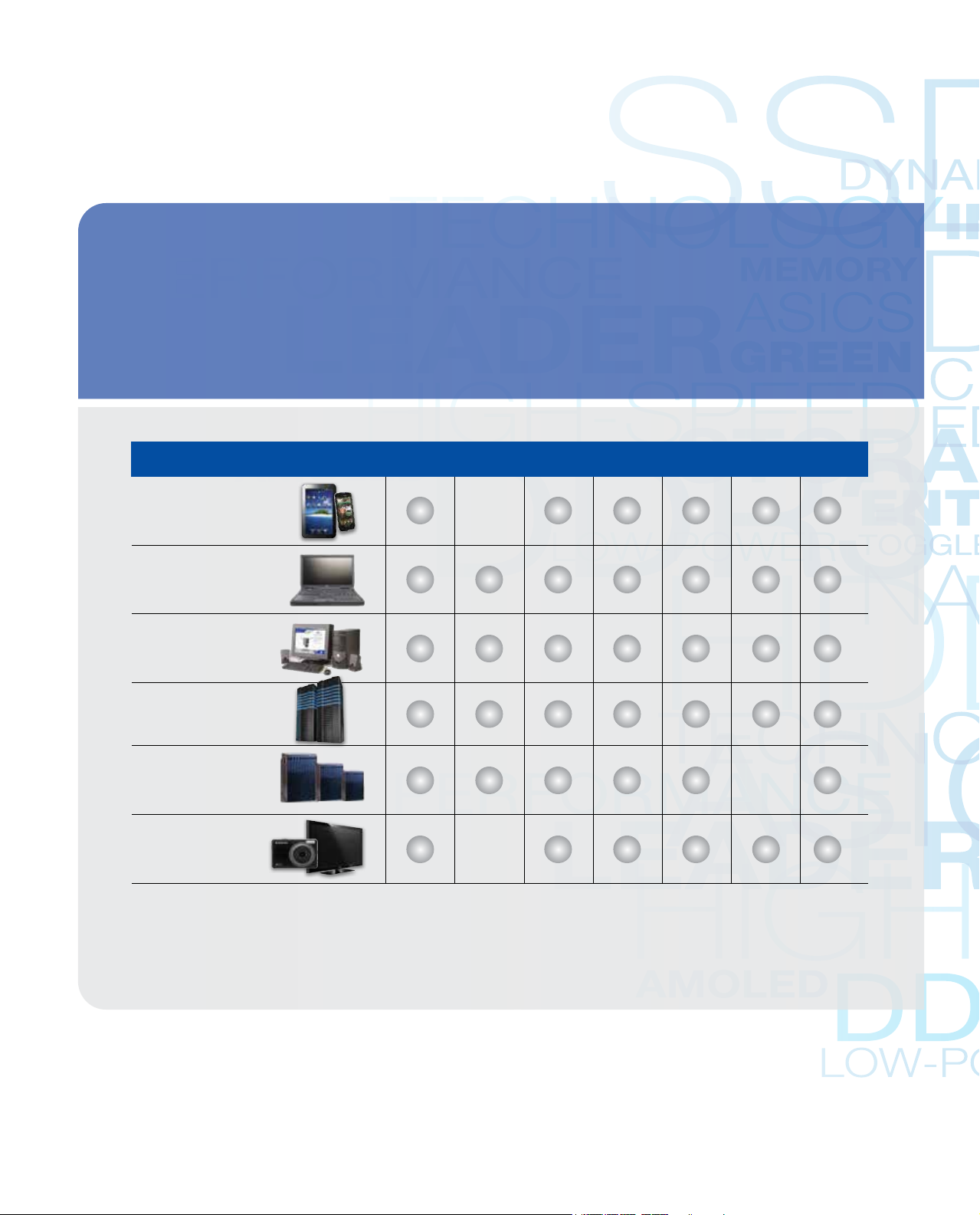
Markets
Mobile/Wireless
Notebook PCs/
Ultrabooks™
Desktop PCs/
Workstations
Servers
Networking/
Communications
Consumer
Electronics
DRAM SSD FLASH ASIC LOGIC TFT/LCD ODD
N/A
N/A
N/A
To access our online sales portal, visit: https://smarttools.ssi.samsung.com
samsung.com/us/oem-solutions
Page 3
DRAM
samsung.com/dram
Pages 4–12
• DDR4 SDRAM
• DDR3 SDRAM
• DDR2 SDRAM
• DDR SDRAM
ASH - SSD
samsung.com/flash
• SLC Flash
• MLC Flash
• microSD Cards
• eMMC
MULTI-ChIP PACKAGES
samsung.com/mcp
• eMMC + LPDDR2
• eMMC + LPDDR3
• eMMC + MDDR
• Mobile DRAM
• Graphics SDRAM
• DRAM Ordering
Information
Pages 13–17
• Solid State Drives (SSD)
• Flash Products Ordering
Information
• Industrial Cards
Page 18–19
DRAM
STORAGE
samsung.com/flash-ssd
• Solid State Drives
samsungodd.com
• Optical Disc Drives
DISPLAyS
samsungdisplay.com
• Exclusive Digital
Information Display (E-DID)
• Performance Digital
Information Display (P-DID)
• Basic Digital Information
Display (B-DID)
CONTACTS
Pages 20–21
Pages 22–24
• Tablets
• Ultrabooks™/PCs
• Monitors
Pages 25–27
samsung.com/dram
2H 2013
samsung.com/us/oem-solutions
• Sales Representatives and Distributors
• To access our online sales portal, visit:
https://smarttools.ssi.samsung.com
3
Page 4
DDR4 SDRAM REGISTERED MODULES
Density Voltage Organization Part Number Composition Compliance Speed (Mbps) Ranks Production
8GB 1.2V 1Gx 72 M393A1G40DB0-CPB 4Gb (1G x4) * 18 Lead Free & Halogen Free, Flip Chip 2133 1 3Q'13
16GB 1.2V 2Gx72
Notes: Register is not fixed yet NA = DDR4-1866 (14-14-14) QB = DDR4-2133(16-16-16) PB = DDR4-2133(15-15-15)
M393A2G40DB0-CPB 4Gb (1G x4) * 36 Lead Free & Halogen Free, Flip Chip 2133
2
3Q'13
DDR4 SDRAM LOAD REDUCED MODULES
Density Voltage Organization Part Number Composition Compliance Speed (Mbps) Ranks Production
32GB 1.2V 4Gx 72
Notes: Register is not fixed yet NA = DDR4-1866 (14-14-14) QB = DDR4-2133(16-16-16) PB = DDR4-2133(15-15-15)
M386A4GDM0-CPB 4Gb MDP (2Gx4) * 36 Lead Free & Halogen Free 2133
4
4Q'13
DDR3 SDRAM REGISTERED MODULES
Density Voltage Organization Part Number Composition Compliance Speed (Mbps) Ranks Production
1GB 1.5V 128Mx72 M393B2873GB0-C(F8/H9/K0/MA)(08/09) 1Gb (128M x8) * 9 Lead Free & Halogen Free, Flip Chip 1066/1333/1600/1866 1 Now
M393B5673GB0-C(F8/H9/K0/MA)(08/09) 1Gb (128M x8) * 18 Lead Free & Halogen Free, Flip Chip 1066/1333/1600/1866 2 Now
2GB 1.5V 256Mx72
4GB 1.5V 512Mx72
8GB 1.5V 1Gx72
16GB 1.5V 2Gx72
32GB 1.5V 4Gx72 M393B4G70BM0-C(F8/H9)(08/09) 8Gb DDP (2G x4) * 36 Lead Free & Halogen Free 1066/1333 4 Now
2GB 1.35V 256Mx72 M393B5773DH0-Y(F8/H9/K0)(08/09) 2Gb (256M x4) * 9 Lead Free & Halogen Free 1066/1333/1600 1 Now
4GB 1.35V 512Mx72
8GB 1.35V 1Gx72
16GB 1.35V 2Gx72
32GB 1.35V 4Gx72
Notes: 04 = IDT B0 register
05 = Inphi C0 register
08 = IDT A1
09 = Inphi UV GS02
* K0 (1600Mbps) available in ES only
M393B5670GB0-C(F8/H9/K0/MA)(08/09) 1Gb (256M x4) * 18 Lead Free & Halogen Free, Flip Chip 1066/1333/1600/1866 1 Now
M393B5773DH0-C(F8/H9/K0/MA)(08/09) 2Gb (256M x8) * 9 Lead Free & Halogen Free 1066/1333/1600/1866 1 Now
M393B5170GB0-C(F8/H9/K0/MA)(08/09) 1Gb (256M x4) * 36 Lead Free & Halogen Free, Flip Chip 1066/1333/1600/1866 2 Now
M393B5273DH0-C(F8/H9/K0/MA)(08/09) 2Gb (256M x8) * 18 Lead Free & Halogen Free 1066/1333/1600/1866 2 Now
M393B5270DH0-C(F8/H9/K0/MA)(08/09) 2Gb (512M x4) * 18 Lead Free & Halogen Free 1066/1333/1600/1866 1 Now
M393B1K73DH0-C(F8/H9)(08/09) 2Gb (256M x8) * 36 Lead Free & Halogen Free 1066/1333 4 Now
M393B1K70DH0-C(F8/H9/K0/MA)(08/09) 2Gb (512M x4) * 36 Lead Free & Halogen Free 1066/1333/1600/1866 2 Now
M393B1K70QB0-C(K0/MA) (08/09) 2Gb (512M x4) * 36 Lead Free & Halogen Free 1600/1866 2 Q3'13
M393B1G70BH0-C(F8/H9/K0/MA)(08/09) 4Gb (1G x4) * 18 Lead Free & Halogen Free 1066/1333 1 Now
M393B1G70QH0-C(K0/MA) (08/09) 4Gb (1G x4) * 18 Lead Free & Halogen Free 1600/1866 1 Q3'13
M393B1G73BH0-C(F8/H9/K0/MA)(08/09) 4Gb (512M x8) * 18 Lead Free & Halogen Free 1066/1333/1600/1866 2 Now
M393B1G70QB0-C(K0/MA) (08/09) 4Gb (1G x4) * 36 Lead Free & Halogen Free 1600/1866 2 Now
M393B2K70DM0-C(F8/H9)(08/09) 2Gb DDP (1G x4) * 36 Lead Free & Halogen Free 1066/1333 4 Now
M393B2G70BH0-C(K0/MA)(08/09) 4Gb (1G x4) * 36 Lead Free & Halogen Free 1600/1866 2 Now
M393B2G70QB0-C(K0/MA)(08/09) 4Gb (1G x4) * 36 Lead Free & Halogen Free 1600/1866 2 Now
M393B2G70DB0-C(K0/MA)(02/03) 4Gb (1G x4) * 36 Lead Free & Halogen Free 1600/1866 2 Now
M393B5173GB0-Y(F8/H9)(08/09) 1Gb (128M x8) * 36 Lead Free & Halogen Free, Flip Chip 1066/1333 4 Now
M393B5170GB0-Y(F8/H9/K0)(08/09) 1Gb (256M x4) * 36 Lead Free & Halogen Free, Flip Chip 1066/1333/1600 2 Now
M393B5273DH0-Y(F8/H9/K0)(08/09) 2Gb (256M x8) * 18 Lead Free & Halogen Free 1066/1333/1600 2 Now
M393B5270DH0-Y(F8/H9/K0)(08/09) 2Gb (512M x4) * 18 Lead Free & Halogen Free 1066/1333/1600 1 Now
M393B1G70BH0-Y(F8/H9/K0)(08/09) 4Gb (1G x4) * 18 Lead Free & Halogen Free 1066/1333/1600 1 Now
M393B1K70QB0-Y(H9/K0) (08/09) 2Gb (512M x4) * 36 Lead Free & Halogen Free 1333/1600 2
M393B1G70QH0-Y(H9/K0) (08/09) 4Gb (1G x4) * 18 Lead Free & Halogen Free 1333/1600 2 Now
Q3'13
M393B1G73BH0-Y(F8/H9/K0)(08/09) 4Gb (512M x8) * 18 Lead Free & Halogen Free 1066/1333/1600 2 Now
M393B2G70BH0-Y(F8/H9/K0)(08/09) 4Gb (1G x4) * 36 Lead Free & Halogen Free 1066/1333/1600 2 Now
M393B2G70BH0-Y(H9/K0) (08/09) 4Gb (1G x4) * 36 Lead Free & Halogen Free 1600/1866 2 Now
M393B2G70QB0-Y(H9/K0) (08/09) 4Gb (1G x4) * 36 Lead Free & Halogen Free 1600/1866 2 Now
M393B2G70DB0-Y(H9/K0) (02/03) 4Gb (1G x4) * 36 Lead Free & Halogen Free 1600/1866 2 Now
M393B2G70QH0-Y(K0) (08/09) 4Gb (1G x4) * 36 Lead Free & Halogen Free 1600/ 1866* 2 Q3'13
M393B2G73BH0-Y(F8/H9)(08/09) 4Gb (512M x8) * 36 Lead Free & Halogen Free 1066/1333 4 Now
M393B2G73BH0-C(F8/H9)(08/09) 4Gb (512M x8) * 36 Lead Free & Halogen Free 1066/1333 4 Now
M393B2K70DM0-Y(F8/H9)(08/09) 4Gb DDP (1G x4) * 36 Lead Free & Halogen Free 1066/1333 4 Now
M393B4G70BM0-Y(F8/H9)(08/09) 8Gb DDP (2G x4) * 36 Lead Free & Halogen Free 1066/1333 4 Now
M393B4G70DM0-YH9(02/03) 8Gb DDP (2G x4) * 36 Lead Free & Halogen Free 1333 4 Q3'13
F8 = DDR3-1066 (7-7-7)
H9 = DDR3-1333 (9-9-9)
K0 = DDR3-1600 (11-11-11)
MA = DDR3-1866 (13-13-13)
4
2H 2013DDR4 & DDR3 SDRAM
samsung.com/dram
samsung.com/dram
Page 5
DDR3 SDRAM LOAD REDUCED REGISTERED MODULES
Density Voltage Organization Part Number Composition Compliance Speed (Mbps) Ranks Production
16GB 1.35V 2Gx72 M386B2K70DM0-YH90 4Gb DDP (1G x4) * 36 Lead Free & Halogen Free 1333 4 Now
32GB 1.35V/1.5V 4Gx72
64GB 1.35V/1,5V 8Gx72
Notes 0 = Inphi iMB GS02A
3 = Inphi iMB GS02B
4 = Montage C1
M386B4G70BM0-YK0(3/4)/
CMA(3/4)
M386B4G70DM0-YK0(3/4)/
CMA(3/4)
M386B8G70BO0-YH94/CK04 4Gb QDP (4G x4) * 36 Lead Free & Halogen Free 1333/1600 8 Now
M386B8G70DE0-YH9(4)/CK0(4) 16Gb QDP (4G x4) * 36 Lead Free & Halogen Free 1333/1600 8 Q3'13
8Gb DDP (2G x4) * 36 Lead Free & Halogen Free 1333/1600/1866 4 Now
8Gb DDP (2G x4) * 36 Lead Free & Halogen Free 1600/1866 4 Q3'13
DDR3 SDRAM VLP REGISTERED MODULES
Density Voltage Organization Part Number Composition Compliance Speed (Mbps) Ranks Production
1GB 1.5V 128Mx72
2GB 1.5V 256Mx72
4GB 1.5V 512Mx72
8GB 1.5V 1Gx72
16GB 1.5V 2Gx72
2GB 1.35V 256Mx72
4GB 1.35V 512Mx72
8GB 1.35V 1Gx72
16GB 1.35V 2Gx72
32GB 1.35V 4Gx72
Notes: 04 = IDT B0 register
05 = Inphi C0 register
08 = IDT A1
09 = Inphi UV GS02
M392B2873GB0-C(F8/H9/K0/MA)(08/09)
M392B5673GB0-C(F8/H9/K0/MA)(08/09)
M392B5670GB0-C(F8/H9/K0/MA)(08/09)
M392B5773DH0-C(F8/H9/K0/MA)(08/09)
M392B5273DH0-C(F8/H9/K0/MA)(08/09)
M392B5270DH0-C(F8/H9/K0/MA)(08/09)
M392B1K73DM0-C(F8/H9)(08/09)
M392B1K70DM0-C(F8/H9/K0/MA)(08/09)
M392B1G73BH0-C(F8/H9/K0/MA)(08/09)
M392B1G73DB0-CMA (08/09) 4Gb (512M x8) * 18 Lead Free & Halogen Free 1866 1 Q3'13
M392B1G70BH0-C(F8/H9/K0/MA)(08/09)
M392B2G70BM0-C(F8/H9/K0/MA)(08/09)
M392B2G70DM0-YK0/CMA (03/04)
M392B2G73BM0-C(F8/H9)(08/09)
M392B5773DH0-Y(F8/H9/K0)(08/09)
1Gb (128M x8) * 9
1Gb (128M x8) * 18
1Gb (256M x8) * 18
2Gb (256M x8) * 9 Lead Free & Halogen Free 1066/1333/1600/1866 1 Now
2Gb (256M x8) * 18 Lead Free & Halogen Free 1066/1333/1600/1866 2 Now
2Gb (512M x4) * 18 Lead Free & Halogen Free 1066/1333/1600/1866 1 Now
2Gb DDP (512M x8) * 18 Lead Free & Halogen Free 1066/1333 4 Now
2Gb DDP (1G x4) * 18 Lead Free & Halogen Free 1066/1333/1600/1866 2 Now
4Gb (512M x8) * 18 Lead Free & Halogen Free 1066/1333/1600/1866 1 Now
4Gb (1G x4) * 18 Lead Free & Halogen Free 1066/1333/1600/1866 1 Now
8Gb DDP (2G x4) * 18 Lead Free & Halogen Free 1066/1333/1600/1866 2 Now
8Gb DDP (2G x4) * 18 Lead Free & Halogen Free 1600/1866 2 Q3'13
4Gb DDP (1G x8) * 18 Lead Free & Halogen Free 1066/1333 4 Now
2Gb (256M x8) * 9 Lead Free & Halogen Free 1066/1333/1600 1 Now
M392B5273DH0-Y(F8/H9/K0)(08/09) 2Gb (256M x8) * 18
M392B5270DH0-Y(F8/H9/K0)(08/09) 2Gb (512M x4) * 18
M392B1K73DM0-Y(F8/H9)(08/09) 4Gb DDP (512M x8) * 18
M392B1K70DM0-Y(F8/H9/K0)(08/09)
M392B1G73BH0-Y(F8/H9/K0)(08/09)
M392B1G73DB0-YK0/CMA (03/04)
M392B1G70BH0-Y(F8/H9/K0)(08/09)
M392B2G70BM0-Y(F8/H9/K0)(08/09) 8Gb DDP (2G x4) * 18 Lead Free & Halogen Free 1066/1333/1600 2 Now
M392B2G70DM0-YK0 (03/04)
M392B4G70BE0-Y(F8/H9)(08)
F8 = DDR3-1066 (7-7-7)
H9 = DDR3-1333 (9-9-9)
K0 = DDR3-1600 (11-11-11)
MA = DDR3-1866 (13-13-13)
2Gb DDP (1G x4) * 18 Lead Free & Halogen Free 1066/1333/1600 2 Now
4Gb (512M x8) * 18 Lead Free & Halogen Free 1066/1333/1600 2 Now
4Gb (512M x8) * 18 Lead Free & Halogen Free 1600/1866 2 Now
4Gb (1G x4) * 18 Lead Free & Halogen Free 1066/1333/1600 1 Now
8Gb DDP (1G x8) * 18 Lead Free & Halogen Free 1600 4 Now
4Gb QDP (4G x4) * 18 Lead Free & Halogen Free 1066/1333 4 Now
Lead Free & Halogen Free,
Flip Chip
Lead Free & Halogen Free,
Flip Chip
Lead Free & Halogen Free,
Flip Chip
Lead Free & Halogen Free
Lead Free & Halogen Free
Lead Free & Halogen Free 1066/1333 4 Now
1066/1333/1600/1866 1 Now
1066/1333/1600/1866 2 Now
1066/1333/1600/1866 1 Now
1066/1333/1600
1066/1333/1600
2 Now
1 Now
DRAM
samsung.com/dram
2H 2013 DDR3 SDRAM
5
Page 6
DDR3 SDRAM UNBUFFERED MODULES
Density Voltage Organization Part Number Composition Compliance Speed (Mbps) Ranks Production
1GB 1.5V 128Mx64 M378B2873GB0-C(F8/H9/K0/MA) 1Gb (128M x8) * 8 Lead Free & Halogen Free, Flip Chip 1066/1333/1600/1866 1 Now
M378B5673GB0-C(F8/H9/K0/MA) 1Gb (128M x8) * 16 Lead Free & Halogen Free, Flip Chip 1066/1333/1600/1866 2 Now
2GB 1.5V 256Mx64
M378B5773DH0-C(F8/H9/K0/MA) 2Gb (256M x8) * 8 Lead Free & Halogen Free 1066/1333/1600/1866 1 Now
M378B5773QB0-CK0/MA 2Gb (256M x8) * 8 Lead Free & Halogen Free 1600/1866 1 Q4'13
M378B5273CH0-C(F8/H9) 2Gb (256M x8) * 16 Lead Free & Halogen Free 1066/1333 2 Now
4GB 1.5V 512Mx64
M378B5273DH0-C(F8/H9/K0/MA) 2Gb (256M x8) * 16 Lead Free & Halogen Free 1066/1333/1600/1866 2 Now
M378B5173QH0-C(K0/MA) 4Gb (512M x8) * 8 Lead Free & Halogen Free 1600/1866 1 Q3'13
M378B5173DB0-C(K0/MA) 4Gb (512M x8) * 8 Lead Free & Halogen Free 1600/1866 1 Now
M378B1G73BH0-C(F8/H9/K0/MA) 4Gb (512M x8) * 16 Lead Free & Halogen Free 1066/1333/1600/1866 2 Now
8GB 1.5V 1024Mx64
M378B1G73QH0-C(K0/MA) 4Gb (512M x8) * 16 Lead Free & Halogen Free 1600/1866 2 Q3'13
M378B1G73DB0-C(K0/MA) 4Gb (512M x8) * 16 Lead Free & Halogen Free 1600/1866 2 Now
DDR3 SDRAM UNBUFFERED MODULES (with ECC)
Density Voltage Organization Part Number Composition Compliance Speed (Mbps) Ranks Production
1GB
2GB 1.5V 256Mx72
4GB 1.5V 512Mx72
8GB 1.5V 1024Mx72
1GB 1.35V 128Mx72
2GB 1.35V 256Mx72
4GB 1.35V 512Mx72
8GB 1.35V 1024Mx72
Notes:
1.5V 128Mx72
F8 = DDR3-1066 (7-7-7)
H9 = DDR3-1333 (9-9-9)
M391B2873GB0-C(F8/H9/K0/MA)
M391B5673GB0-C(F8/H9/K0/MA)
M391B5773CH0-C(F8/H9)
M391B5773DH0-C(F8/H9/K0/MA)
M391B5273CH0-C(F8/H9)
M391B5273DH0-C(F8/H9/K0/MA)
M391B1G73BH0-C(F8/H9/K0/MA)
M391B1G73QH0-C(MA)
M391B2873GB0-Y(F8/H9/K0)
M391B5673GB0-Y(F8/H9/K0)
M391B5773CH0-Y(F8/H9)
M391B5773DH0-Y(F8/H9/K0) 2Gb (256M x8) * 9 Lead Free & Halogen Free 1066/1333/1600 1 Now
M391B5273CH0-Y(F8/H9)
M391B5273DH0-Y(F8/H9/K0)
M391B5173QH0-YK0
M391B1G73BH0-Y(F8/H9/K0)
M391B1G73QH0-YK0
K0 = DDR3-1600 (11-11-11)
MA = DDR3-1866 (13-13-13)
1Gb (128M x8) * 9
1Gb (128M x8) * 18
2Gb (256M x8) * 9 Lead Free & Halogen Free 1066/1333 1 Now
2Gb (256M x8) * 9 Lead Free & Halogen Free 1066/1333/1600/1866 1 Now
2Gb (256M x8) * 18 Lead Free & Halogen Free 1066/1333 2 Now
2Gb (256M x8) * 18 Lead Free & Halogen Free 1066/1333/1600/1866 2 Now
4Gb (512M x8) * 18 Lead Free & Halogen Free
4Gb (512M x8) * 18 Lead Free & Halogen Free 1866 2 Q3'13
1Gb (128M x8) * 9
1Gb (128M x8) * 18
2Gb (256M x8) * 9 Lead Free & Halogen Free 1066/1333 1 Now
2Gb (256M x8) * 18 Lead Free & Halogen Free 1066/1333 2 Now
2Gb (256M x8) * 18 Lead Free & Halogen Free 1066/1333/1600 2 Now
4Gb (512M x8) * 9 Lead Free & Halogen Free 1600 1 Q3'13
4Gb (512M x8) * 18 Lead Free & Halogen Free 1066/1333/1600 2 Now
4Gb (512M x8) * 18 Lead Free & Halogen Free
Lead Free & Halogen Free,
Flip Chip
Lead Free & Halogen Free,Flip
Chip
Lead Free & Halogen Free,
Flip Chip
Lead Free & Halogen Free,Flip
Chip
1066/1333/1600/1866 1 Now
1066/1333/1600/1866 2 Now
1066/1333/1600/1866
1066/1333/1600 1 Now
1066/1333/1600 2 Now
1600
2 Now
2 Q3'13
6
2H 2013DDR3 SDRAM
samsung.com/dram
Page 7
DDR3 SDRAM SODIMM MODULES
Density Voltage Organization Part Number Composition Compliance Speed (Mbps) Ranks Production
1GB 1.5V 128Mx64 M471B2873GB0-C(F8/H9/K0/MA) 1Gb (128M x8) * 8 Lead Free & Halogen Free, Flip Chip 1066/1333/1600/1866 1 Now
2GB 1.5V 256Mx64 M471B5673GB0-C(F8/H9/K0/MA) 1Gb (128M x8) * 16 Lead Free & Halogen Free, Flip Chip 1066/1333/1600/1866 2 Now
M471B5773DH0-C(F8/H9/K0/MA) 2Gb (256M x8) * 8 Lead Free & Halogen Free 1066/1333/1600/1866 1 Now
4GB 1.5V 512Mx64
8GB 1.5V 1024Mx64 M471B1G73BH0-C(F8/H9/K0/MA) 4Gb (512M x8) * 16 Lead Free & Halogen Free 1066/1333/1600/1866 2 Now
1GB 1.35V 128Mx64 M471B2873GB0-Y(F8/H9/K0) 1Gb (128M x8) * 8 Lead Free & Halogen Free, Flip Chip 1066/1333/1600/1866 1 Now
2GB 1.35V 256Mx64
4GB 1.35V 512Mx64
8GB 1.35V 1024Mx64
Notes:
F8 = DDR3-1066 (7-7-7)
H9 = DDR3-1333 (9-9-9)
M471B5273DH0-C(F8/H9/K0/MA) 2Gb (256M x8) * 16 Lead Free & Halogen Free 1066/1333/1600/1866 2 Now
M471B5173BH0-C(F8/H9/K0/MA) 4Gb (512M x8) * 8 Lead Free & Halogen Free 1066/1333/1600/1866 1 Now
M471B5673GB0-Y(F8/H9/K0) 1Gb (128M x8) * 16 Lead Free & Halogen Free, Flip Chip 1066/1333/1600 2 Now
M471B5773DH0-Y(F8/H9/K0) 2Gb (256M x8) * 8 Lead Free & Halogen Free 1066/1333/1600 1 Now
M471B5674QH0-YK0 4Gb (256M x16) * 4 Lead Free & Halogen Free 1600 1 Q4'13
M471B5273DH0-Y(F8/H9/K0) 2Gb (256M x8) * 16 Lead Free & Halogen Free 1066/1333/1600 2 Now
M471B5173BH0-Y(F8/H9/K0) 4Gb (512M x8) * 8 Lead Free & Halogen Free 1066/1333/1600 1 Now
M471B5173QH0-YK0 4Gb (512M x8) * 8 Lead Free & Halogen Free 1600 1 Q3'13
M471B5173DB0-YK0 4Gb (512M x8) * 8 Lead Free & Halogen Free 1600 1 Q3'13
M471B1G73BH0-Y(F8/H9/K0) 4Gb (512M x8) * 16 Lead Free & Halogen Free 1066/1333/1600 2 Now
M471B1G73QH0-YK0 4Gb (512M x8) * 16 Lead Free & Halogen Free 1600 2 Q3'13
M471B1G73DB0-YK0 4Gb (512M x8) * 16 Lead Free & Halogen Free 1600 2 Q3'13
K0 = DDR3-1600 (11-11-11)
MA = DDR3-1866 (13-13-13)
DRAM
DDR3 SDRAM ECC SODIMM MODULES
Density Organization Part Number Composition Compliance Speed (Mbps) Register Rank Production
2GB 1.35V 256Mx64 M474B5773DH0-YH9/K0 2Gb x8*9 Lead Free & Halogen Free 1333/1600 1 Now
4GB 1.35V 512Mx64
8GB 1.35V 1024Mx64
Notes: E6 = PC2-5300 (DDR2-667 @ CL=5)
F7 = PC2-6400 (DDR2-800 @ CL=6)
E7 = PC2-6400 (DDR2-800 @ CL=5)
M474B5273DH0-YH9/K0 2Gb x8*18 Lead Free & Halogen Free 1333/1600 2 Now
M474B5173BH0-YH9/K0 4Gb x8*9 Lead Free & Halogen Free 1333/1600 1 Now
M474B1G73BH0-YH9/K0 4Gb x8*18 Lead Free & Halogen Free 1333/1600 2 Now
M474B1G73QH0-YK0 4Gb x8*18 Lead Free & Halogen Free 1600 2 Q3'13
M474B1G73QH0-CMA 4Gb x8*18 Lead Free & Halogen Free 1866 2 Q3'13
samsung.com/dram
2H 2013 DDR3 SDRAM
7
Page 8
DDR3 SDRAM COMPONENTS
Density Voltage Organization Part Number # Pins-Package Compliance Speed (Mbps) Dimensions Production
256M x4 K4B1G0446G-BC(F8/H9/K0/MA) 78 Ball -FBGA
1Gb 1.5V
2Gb 1.5V
4Gb 1.5V
1Gb
2Gb 1.35V
4Gb 1.35V
Notes:
128M x8 K4B1G0846G-BC(F8/H9/K0/MA) 78 Ball -FBGA
128M x16 K4B1G1646G-BC(F8/H9/K0/MA/NB) 96 Ball -FBGA
K4B2G0446C-HC(F8/H9/K0) 78 Ball -FBGA Lead Free & Halogen Free 1066/1333/1600 7.5x11mm Now
512M x4
256M x8
128M x16
1G x4
512M x8
256Mx16
1.35V 256M x4
1.35V 128M x8
512M x4
256M x8
1G x4
512M x8
256Mx16
F8 = DDR3-1066 (7-7-7)
H9 = DDR3-1333 (9-9-9)
K4B2G0446D-HC(F8/H9/K0/MA) 78 Ball -FBGA Lead Free & Halogen Free 1066/1333/1600/1866 7.5x11mm Now
K4B2G0446Q-BC(K0/MA) 78 Ball -FBGA
K4B2G0846C-HC(F8/H9/K0) 78 Ball -FBGA Lead Free & Halogen Free 1066/1333/1600 7.5x11mm Now
K4B2G0846D-HC(F8/H9/K0/MA) 78 Ball -FBGA Lead Free & Halogen Free 1066/1333/1600/1866 7.5x11mm Now
K4B2G0846Q-BC(K0/MA) 78 Ball -FBGA
K4B2G1646C-HC(F8/H9/K0/MA) 96 Ball -FBGA Lead Free & Halogen Free 1066/1333/1600/1866 7.5x13.3mm Now
K4B2G1646E-BC(F8/H9/K0/MA) 96 Ball -FBGA Lead Free & Halogen Free 1066/1333/1600/1866 7.5x13.3mm Now
K4B2G1646Q-B(K0/MA/NB) 96 Ball -FBGA Lead Free & Halogen Free 1600/1866/2133 7.5x13.3mm Q3'13
K4B4G0446B-HC(F8/H9/K0/MA) 78 Ball -FBGA Lead Free & Halogen Free 1066/1333/1600/1866 10x11mm Now
K4B4G0446Q-HC(K0/MA) 78 Ball -FBGA Lead Free & Halogen Free 1600/1866 10x11mm Now
K4B4G0846B-HC(F8/H9/K0/MA) 78 Ball -FBGA Lead Free & Halogen Free 1066/1333/1600/1866 10x11mm Now
K4B4G0846D-HC(K0/MA) 78 Ball -FBGA Lead Free & Halogen Free 1600/1866 7.5x11mm Now
K4B4G0846Q-HC(K0/MA) 78 Ball -FBGA Lead Free & Halogen Free 1600/1866 10x11mm Now
K4B4G1646B-HC(F8/H9/K0/MA) 96 Ball -FBGA Lead Free & Halogen Free 1333/1600/1866/2133 10x13.3mm Now
K4B4G1646D-BC(K0/MA) 96 Ball -FBGA Lead Free & Halogen Free 1600/1866 7.5x13.3mm Q3'13
K4B1G0446F-HY(F8/H9/K0) 78 Ball -FBGA Lead Free & Halogen Free 1066/1333/1600 7.5x11mm Now
K4B1G0446G-BY(F8/H9/K0) 78 Ball -FBGA
K4B1G0846F-HY(F8/H9/K0) 78 Ball -FBGA Lead Free & Halogen Free 1066/1333/1600 7.5x11mm Now
K4B1G0846G-BY(F8/H9/K0) 78 Ball -FBGA
K4B2G0446C-HY(F8/H9/K0) 78 Ball -FBGA Lead Free & Halogen Free 1066/1333/1600 7.5x11mm Now
K4B2G0446D-HY(F8/H9/K0) 78 Ball -FBGA Lead Free & Halogen Free 1066/1333/1600 7.5x11mm Now
K4B2G0446Q-BY(K0) 78 Ball -FBGA
K4B2G0846C-HY(F8/H9/K0) 78 Ball -FBGA Lead Free & Halogen Free 1066/1333/1600 7.5x11mm Now
K4B2G0846D-HY(F8/H9/K0) 78 Ball -FBGA Lead Free & Halogen Free 1066/1333/1600 7.5x11mm Now
K4B2G0846Q-BY(K0) 78 Ball -FBGA
K4B4G0446B-HY(F8/H9/K0) 78 Ball -FBGA Lead Free & Halogen Free 1066/1333/1600 10x11mm Now
K4B4G0446D-HY(K0) 78 Ball -FBGA Lead Free & Halogen Free 1600 7.5x11mm Now
K4B4G0446Q-HY(K0) 78 Ball -FBGA Lead Free & Halogen Free 1600 10x11mm Now
K4B4G0846B-HY(F8/H9/K0/MA) 78 Ball -FBGA Lead Free & Halogen Free 1066/1333/1600/1866 10x11mm Now
K4B4G0846D-BC(K0/MA) 78 Ball -FBGA Lead Free & Halogen Free 1600/1866 10x11mm Q3'13
K4B4G0846D-HY(K0) 78 Ball -FBGA Lead Free & Halogen Free 1600 7.5x11mm Now
K4B4G0846Q-HY(K0) 78 Ball -FBGA Lead Free & Halogen Free 1600 10x11mm Now
K4B4G1646B-HY(K0/MA) 96 Ball -FBGA Lead Free & Halogen Free 1333/1600/1866/2133 10x13.3mm Now
K4B4G1646D-BY(K0/MA) 96 Ball -FBGA Lead Free & Halogen Free 1600/1866 7.5x13.3mm Q3'13
K0 = DDR3-1600 (11-11-11)
MA = DDR3-1866 (13-13-13)
NB = DDR3-2133 (14-14-14)
Lead Free & Halogen Free,
Flip Chip
Lead Free & Halogen Free,
Flip Chip
Lead Free & Halogen Free,
Flip Chip
Lead Free & Halogen Free,
Flip Chip
Lead Free & Halogen Free,
Flip Chip
Lead Free & Halogen Free,
Flip Chip
Lead Free & Halogen Free,
Flip Chip
Lead Free & Halogen Free,
Flip Chip
Lead Free & Halogen Free,
Flip Chip
1066/1333/1600/1866 7.5x11mm Now
1066/1333/1600/1866 7.5x11mm Now
1066/1333/1600/1866/2133 7.5x13.3mm Now
1600/1866 7.5x11mm Now
1600/1866 7.5x11mm Now
1066/1333/1600 7.5x11mm Now
1066/1333/1600 7.5x11mm Now
1600 7.5x11mm Now
1600 7.5x11mm Now
DDR2 SDRAM COMPONENTS
Density Organization Part Number # Pins-Package Dimensions Package Speed (Mbps) Production
256Mb 16Mx16 K4T56163QN-HC(E6/F7/E7/F8) 84-FBGA 7.5x12.5mm Lead free & Halogen free 667/800/1066 Now
128M x4 K4T51043QJ-HC(E6/F7/E7) 60-FBGA 7.5x9.5mm Lead free & Halogen free 667/800 Now
512Mb
1Gb
64M x8 K4T51083QJ-HC(E6/F7/E7/F8) 60-FBGA 7.5x9.5mm Lead free & Halogen free 667/800/1066 Now
32M x16 K4T51163QJ-HC(E6/F7/E7/F8) 84-FBGA 7.5x12.5mm Lead free & Halogen free 667/800/1066 Now
256M x4 K4T1G044QF-BC(E6/F7/E7) 60-FBGA 7.5x9.5mm Lead free & Halogen free 667/800 Now
128M x8 K4T1G084QF-BC(E6/F7/E7/F8) 60-FBGA 7.5x9.5mm Lead free & Halogen free 667/800/1066 Now
64M x16 K4T1G164QF-BC(E6/F7/E7/F8) 84-FBGA 7.5x12.5mm Lead free & Halogen free 667/800/1066 Now
DDR3, DDR2 & DDR SDRAM Components
8
2H 2013
samsung.com/dram
Page 9
DDR SDRAM COMPONENTS
Density Organization Part Number # Pins - Package Speed (Mbps)
128Mx4
512Mb
Notes: B0 = DDR266 (133MHz @ CL=2.5) A2 = DDR266 (133MHz @ Cl=2) B3 = DDR333 (166MHz @ CL=2.5) CC = DDR400 (200MHz @ CL=3)
64Mx8
32Mx16 K4H511638J-LCCC/B3 66-TSOP 333/400
K4H510438J-LCB3/B0 66-TSOP 266/333
K4H510438J-BCCC/B3 60-FBGA 333/400
K4H510838J-LCCC/B3 66-TSOP 333/400
K4H510838J-BCCC/B3 60-FBGA 333/400
MOBILE DRAM COMPONENTS
Density Type Organization Part Number Package Power Production
512Mb
2Gb 64Mx32 K4X2G323PD-8GD8 90-FBGA, 200MHz 1.8V Now
4Gb x32 (2CS, 2CKE) K4X4G303PD-AGD8 168-FBGA, 12x12 PoP, DDP, 200MHz 1.8V Now
2Gb
4Gb
8Gb
16Gb
4Gb
8Gb
16Gb
MDDR
LPDDR2
LPDDR3
32Mx16 K4X51163PK-FGD8 60-FBGA, 200MHz 1.8V Now
16Mx32 K4X51323PK-8GD8 90-FBGA, 200MHz 1.8V Now
1CH x32 K4P2G324ED-AGC1 168-FBGA, 12x12 PoP, MONO, 800Mbps 1.8V/1.2V/1.2V Now
1CH x32 K4P4G324EQ-AGC2 168-FBGA, 12x12 PoP, MONO, 1066Mbps 1.8V/1.2V/1.2V Now
1CH x32 K4P4G324EQ-FGC2 134-FBGA, 11x11.5 , MONO, 1066Mbps 1.8V/1.2V/1.2V Now
1CH x32 K4P8G304EQ-AGC2 168-FBGA, 12x12 PoP, DDP, 1066Mbps 1.8V/1.2V/1.2V Now
1CH x32 K4P8G304EQ-PGC2 216-FBGA, 12x12 PoP, DDP, 1066Mbps 1.8V/1.2V/1.2V Now
2CH x32 K3PE7E70QM-BGC2 216-FBGA, 12x12 PoP, DDP, 1066Mbps 1.8V/1.2V/1.2V Now
2CH x32 K3PE7E70QM-CGC2 220-FBGA, 14x14 PoP, DDP, 1066Mbps 1.8V/1.2V/1.2V Now
2CH x32 K3PE0E00QM-BGC2 216-FBGA, 12x12 PoP, QDP, 1066Mbps 1.8V/1.2V/1.2V Now
2CH x32 K3PE0E00QM-CGC2 220-FBGA, 14x14 PoP, QDP, 1066Mbps 1.8V/1.2V/1.2V Now
1CH x32 K4E4E324ED-EGCE 178-FBGA, 11x11.5, MONO , 1600Mbps 1.8V/1.2V/1.2V CS
1CH x32 K4E8E304ED-EGCE 178-FBGA, 11x11.5, DDP, 1600Mbps 1.8V/1.2V/1.2V CS
2CH x32 K3QF1F10DM-AGCE 253-FBGA, 11x11.5, DDP, 1600Mbps 1.8V/1.2V/1.2V CS
2CH x32 K3QF1F10DA-QGCE 216-FBGA, 15x15 PoP, DDP, 1600Mbps 1.8V/1.2V/1.2V Now
1CH x32 K4E6E304ED-EGCE 178-FBGA, 11x11.5, QDP, 1600Mbps 1.8V/1.2V/1.2V CS
2CH x32 K3QF2F20DM-AGCE 253-FBGA, 11x11.5, QDP, 1600Mbps 1.8V/1.2V/1.2V CS
2CH x32 K3QF2F20DM-FGCE 256-FBGA, 14x14 PoP, QDP, 1600Mbps 1.8V/1.2V/1.2V CS
2CH x32 K3QF2F20DA-QGCE 216-FBGA, 15x15 PoP, QDP, 1600Mbps 1.8V/1.2V/1.2V Now
DRAM
GRAPHICS DRAM COMPONENTS
Type Density Organization Part Number Package VDD/VDDQ Speed Bin (MHz) Production
4Gb
GDDR5
GDDR3 1Gb 32Mx32 K4J10324KG-HC(14/1A) 136-FBGA 1.8V/1.8V 1400/2000 Now
gDDR3
Notes: Package (1) Speeds (clock cycle - speed bin)
samsung.com/dram
2Gb
1Gb
4Gb 256Mx16
2Gb 128Mx16
1Gb 64Mx16 K4W1G1646G-BC(15/12/11/1A) 96-FBGA 1.5V/1.5V 1333/1600/1866/2133 Now
H: FBGA (Halogen Free & Lead Free) (DDR3)
B: FCFBGA (Halogen Free & Lead Free) (DDR3)
H: FCFBGA (Halogen Free & Lead Free) (GDDR5)
F: FBGA (Halogen Free & Lead Free) (GDDR5)
128Mx32 K4G41325FC-HC(04/03/28) 170-FCFBGA 1.5V/1.5V 5000/6000/7000 Now
K4G41325FC-HC(04/03) 170-FCFBGA 1.35V/1.35V 4000/5000 Now
64Mx32 K4G20325FD-FC(04/03/28) 170-FBGA 1.5V/1.5V 5000/6000/7000 Now
K4G20325FD-FC(04/03) 170-FBGA 1.35V/1.35V 4000/5000 Now
32Mx32 K4G10325FG-HC(03) 170-FCFBGA 1.6V/1.6V 6000 Now
K4G10325FG-HC(05/04) 170-FCFBGA 1.5V/1.5V 4000/5000 Now
K4G10325FG-HC(04/03) 170-FCFBGA 1.35V/1.35V 4000/5000 Now
K4W4G1646D-BC(12/11/1A) 96-FCFBGA 1.5V/1.5V 1600/1866/2133 Now
K4W4G1646D-BC(1A) 96-FCFBGA 1.35V/1.35V 1866
K4W4G1646D-BY(12) 96-FCFBGA 1.35V/1.35V 1600
K4W4G1646B-HC(12/11/1A) 96-FBGA 1.5V/1.5V 1600/1866/2133 Now
K4W2G1646Q-BC(12/11/1A) 96-FCFBGA 1.5V/1.5V 1600/1866/2133 Now
K4W2G1646Q-BC(1A) 96-FCFBGA 1.35V/1.35V 1866
K4W2G1646Q-BY(12) 96-FCFBGA 1.35V/1.35V 1600
K4W2G1646E-BC(15/12/11/1A) 96-FBGA 1.5V/1.5V 1333/1600/1866/2133 Now
28: 0.28ns (7000Mbps)
03: 0.3ns (6000Mbps)
04: 0.4ns (5000Mbps)
05: 0.5ns (4000Mbps)
2H 2013 Mobile & Graphics DRAM Components
1A: 1.0ns (2000Mbps GDDR3)
14: 1.4ns (1400Mbps GDDR3)
1A: 1.0ns (2133Mbps gDDR3)
11: 1.1ns (1866Mbps)
12: 1.25ns (1600Mbps)
9
Page 10

COMPONENT DRAM ORDERING INFORMATION
1 2 3 4 5 6 7 8 9 10 11
K 4 T XX XX X X X X X XX
SAMSUNG Memory
DRAM
DRAM Type
Density
Bit Organization
1. Memory (K)
2. DRAM: 4
3. DRAM Type
B: DDR3 SDRAM
D: GDDR SDRAM
G: GDDR5 SDRAM
H: DDR SDRAM
J: GDDR3 SDRAM
M: Mobile SDRAM
N: SDDR2 SDRAM
S: SDRAM
T: DDR SDRAM
U: GDDR4 SDRAM
V: Mobile DDR SDRAM Power Efficient Address
W: SDDR3 SDRAM
X: Mobile DDR SDRAM
Y: XDR DRAM
Z: Value Added DRAM
4. Density
10: 1G, 8K/32ms
16: 16M, 4K/64ms
26: 128M, 4K/32ms
28: 128M, 4K/64ms
32: 32M, 2K/32ms
50: 512M, 32K/16ms
51: 512M, 8K/64ms
52: 512M, 8K/32ms
54: 256M, 16K/16ms
55: 256M, 4K/32ms
56: 256M, 8K/64ms
62: 64M, 2K/16ms
64: 64M, 4K/64ms
68: 768M, 8K/64ms
1G: 1G, 8K/64ms
2G: 2G, 8K/64ms
4G: 4G, 8K/64ms
5. Bit Organization
02: x2
04: x4
06: x4 Stack (Flexframe)
07: x8 Stack (Flexframe)
08: x8
15: x16 (2CS)
16: x16
26: x4 Stack (JEDEC Standard)
27: x8 Stack (JEDEC Standard)
30: x32 (2CS, 2CKE)
31: x32 (2CS)
32: x32
6. # of Internal Banks
2: 2 Banks
3: 4 Banks
4: 8 Banks
5: 16 Banks
7. Interface ( VDD, VDDQ)
2: LVTTL, 3.3V, 3.3V
4: LVTTL, 2.5V, 2.5V
5: SSTL-2 1.8V, 1.8V
6: SSTL-15 1.5V, 1.5V
8: SSTL-2, 2.5V, 2.5V
A: SSTL, 2.5V, 1.8V
F: POD-15 (1.5V,1.5V)
H: SSTL_2 DLL, 3.3V, 2.5V
M: LVTTL, 1.8V, 1.5V
N: LVTTL, 1.5V, 1.5V
P: LVTTL, 1.8V, 1.8V
Q: SSTL-2 1.8V, 1.8V
R: SSTL-2, 2.8V, 2.8V
U: DRSL, 1.8V, 1.2V
8. Generation
A: 2nd Generation
B: 3rd Generation
C: 4th Generation
D: 5th Generation
E: 6th Generation
F: 7th Generation
G: 8th Generation
H: 9th Generation
I: 10th Generation
J: 11th Generation
K: 12th Generation
M: 1st Generation
N: 14th Generation
Q: 17th Generation
Speed
Temp & Power
Package Type
Generation
Interface (VDD, VDDQ)
Number of Internal Banks
9. Package Type
DDR2 DRAM
L: TSOP II (Lead-free & Halogen-free)
H: FBGA (Lead-free & Halogen-free)
F: FBGA for 64Mb DDR (Lead-free & Halogen-free)
6: sTSOP II (Lead-free & Halogen-free)
T: TSOP II
N: sTSOP II
G: FBGA
U: TSOP II (Lead-free)
V: sTSOP II (Lead-free)
Z: FBGA (Lead-free)
DDR2 SDRAM
Z: FBGA (Lead-free)
J: FBGA DDP (Lead-free)
Q: FBGA QDP (Lead-free)
H: FBGA (Lead-free & Halogen-free)
M: FBGA DDP (Lead-free & Halogen-free)
E: FBGA QDP (Lead-free & Halogen-free)
T: FBGA DSP (Lead-free & Halogen-free, Thin)
DDR3 SDRAM
Z: FBGA (Lead-free)
H: FBGA (Halogen-free & Lead-free)
Graphics Memory
Q: TQFP
U: TQFP (Lead Free)
G: 84/144 FBGA
V: 144 FBGA (Lead Free)
Z: 84 FBGA (Lead Free)
T: TSOP
L: TSOP (Lead Free)
A: 136 FBGA
B: 136 FBGA (Lead Free)
H: FBGA (Hologen Free & Lead Free)
E: 100 FBGA (Hologen Free & Lead Free)
SDRAM
L TSOP II (Lead-free & Halogen-free)
N: STSOP II
T: TSOP II
U: TSOP II (Lead-free)
V: sTSOP II (Lead-free)
10
2H 2013DRAM Ordering Information
samsung.com/dram
Page 11

COMPONENT DRAM ORDERING INFORMATION
1 2 3 4 5 6 7 8 9 10 11
K 4 T XX XX X X X X X XX
SAMSUNG Memory
DRAM
DRAM Type
Density
Bit Organization
XDR DRAM
J: BOC(LF) P: BOC
Mobile DRAM
Leaded/Lead Free
G/A: 52balls FBGA Mono
R/B: 54balls FBGA Mono
X/Z: 54balls BOC Mono
J/V: 60(72)balls FBGA Mono 0.5pitch
L /F: 60balls FBGA Mono 0.8pitch
S/D: 90balls FBGA
Monolithic (11mm x 13mm)
F/H: Smaller 90balls FBGA Mono
Y/P: 54balls CSP DDP
M/E: 90balls FBGA DDP
10. Temp & Power - COMMON
(Temp, Power)
C: Commercial, Normal (0’C – 95’C) & Normal
Power
C: (Mobile Only) Commercial (-25 ~ 70’C), Normal
Power
J: Commercial, Medium
L: Commercial, Low (0’C – 95’C) & Low Power
L: (Mobile Only) Commercial, Low, i-TCSR
F: Commercial, Low, i-TCSR & PASR & DS
E: Extended (-25~85’C), Normal
N: Extended, Low, i-TCSR
G: Extended, Low, i-TCSR & PASR & DS
I: Industrial, Normal (-40’C – 85’C) & Normal
Power
P: Industrial, Low (-40’C – 85’C) & Low Power
H: Industrial, Low, i-TCSR & PASR & DS
11. Speed (Wafer/Chip Biz/BGD: 00)
DDR SDRAM
CC: DDR400 (200MHz @ CL=3, tRCD=3, tRP=3)
B3: DDR333 (166MHz @ CL=2.5, tRCD=3,
tRP=3) *1
A2: DDR266 (133MHz @ CL=2 , tRCD=3, tRP=3)
B0: DDR266 (133MHz @ CL=2.5, tRCD=3,
tRP=3)
Note 1: "B3" has compatibility with "A2" and "B0"
DDR2 SDRAM
CC: DDR2-400 (200MHz @ CL=3, tRCD=3,
tRP=3)
D5: DDR2-533 (266MHz @ CL=4, tRCD=4,
tRP=4)
E6: DDR2-667 (333MHz @ CL=5, tRCD=5,
tRP=5)
F7: DDR2-800 (400MHz @ CL=6, tRCD=6,
tRP=6)
E7: DDR2-800 (400MHz @ CL=5, tRCD=5,
tRP=5)
DDR3 SDRAM
F7: DDR3-800 (400MHz @ CL=6, tRCD=6,
tRP=6)
F8: DDR3-1066 (533MHz @ CL=7, tRCD=7,
tRP=7)
G8: DDR3-1066 (533MHz @ CL=8, tRCD=8,
tRP=8)
H9: DDR3-1333 (667MHz @ CL=9, tRCD=9,
tRP=9)
K0: DDR3-1600 (800MHz @ CL=11, tRCD=11,
tRP=11)
MA: DDR3-1866 (933MHz @ CL=13, tRCD=13,
tRP=13)
NB: DDR3-2133 (1067MHz @ CL=14, tRCD=14,
tRP=14)
Graphics Memory
18: 1.8ns (550MHz)
04: 0.4ns (2500MHz)
20: 2.0ns (500MHz)
05: 0.5ns (2000MHz)
22: 2.2ns (450MHz)
5C: 0.56ns (1800MHz)
25: 2.5ns (400MHz)
06: 0.62ns (1600MHz)
2C: 2.66ns (375MHz)
6A: 0.66ns (1500MHz)
2A: 2.86ns (350MHz)
07: 0.71ns (1400MHz)
33: 3.3ns (300MHz)
7A: 0.77ns (1300MHz)
36: 3.6ns (275MHz)
08: 0.8ns (1200MHz)
40: 4.0ns (250MHz)
DRAM
Speed
Temp & Power
Package Type
Generation
Interface (VDD, VDDQ)
Number of Internal Banks
09: 0.9ns (1100MHz)
45: 4.5ns (222MHz)
1 : 1.0ns (1000MHz)
50/5A: 5.0ns (200MHz)
1 : 1.1ns (900MHz)
55: 5.5ns (183MHz)
12: 1.25ns (800MHz)
60: 6.0ns (166MHz)
14: 1.4ns (700MHz)
16: 1.6ns (600MHz)
SDRAM (Default CL=3)
50: 5.0ns (200MHz CL=3)
60: 6.0ns (166MHz CL=3)
67: 6.7ns
75: 7.5ns PC133 (133MHz CL=3)
XDR DRAM
A2: 2.4Gbps, 36ns, 16Cycles
B3: 3.2Gbps, 35ns, 20Cycles
C3: 3.2Gbps, 35ns, 24Cycles
C4: 4.0Gbps, 28ns, 24Cycles
DS: Daisychain Sample
Mobile-SDRAM
60: 166MHz, CL 3
75: 133MHz, CL 3
80: 125MHz, CL 3
1H: 105MHz, CL 2
1L: 105MHz, CL 3
15: 66MHz, CL 2 & 3
Mobile-DDR
C3: 133MHz, CL 3
C2: 100MHz, CL 3
C0: 66MHz, CL 3
Note: All Lead-free and Halogen-free products are in
compliance with RoHS
samsung.com/dram
2H 2013 DRAM Ordering Information
11
Page 12

MODULE DRAM ORDERING INFORMATION
1 2 3 4 5 6 7 8 9 10 11 12 13
M X XX T XX X X X X X X XX X
SAMSUNG Memory
DIMM
Data bits
DRAM Component Type
Depth
Number of Banks
Bit Organization
1. Memory Module: M
2. DIMM Type
3: DIMM
4: SODIMM
3. Data bits
12: x72 184pin Low Profile Registered DIMM
63: x63 PC100/PC133 μSODIMM with SPD for
144pin
64: x64 PC100/PC133 SODIMM with SPD for
144pin (Intel/JEDEC)
66: x64 Unbuffered DIMM with SPD for
144pin/168pin (Intel/JEDEC)
68: x64 184pin Unbuffered DIMM
70: x64 200pin Unbuffered SODIMM
71: x64 204pin Unbuffered SODIMM
74: x72/ECC Unbuffered DIMM with SPD for 168pin
(Intel/JEDEC)
77: x72/ECC PLL + Register DIMM with SPD for
168pin (Intel PC100)
78: x64 240pin Unbuffered DIMM
81: x72 184pin ECC unbuffered DIMM
83: x72 184pin Registered DIMM
90: x72/ECC PLL + Register DIMM
91: x72 240pin ECC unbuffered DIMM
92: x72 240pin VLP Registered DIMM
93: x72 240pin Registered DIMM
95: x72 240pin Fully Buffered DIMM with SPD for
168pin (JEDEC PC133)
4. DRAM Component Type
B: DDR3 SDRAM (1.5V VDD)
L: DDR SDRAM (2.5V VDD)
S: SDRAM
T: DDR2 SDRAM (1.8V VDD)
5. Depth
09: 8M (for 128Mb/512Mb)
17: 16M (for 128Mb/512Mb)
16: 16M
28: 128M
29: 128M (for 128Mb/512Mb)
32: 32M
33: 32M (for 128Mb/512Mb)
51: 512M
52: 512M (for 512Mb/2Gb)
56: 256M
57: 256M (for 512Mb/2Gb)
59: 256M (for 128Mb/512Mb)
64: 64M
65: 64M (for 128Mb/512Mb)
1G: 1G
1K: 1G (for 2Gb)
6. # of Banks in Comp. & Interface
1: 4K/64mxRef., 4Banks & SSTL-2
2 : 8K/64ms Ref., 4Banks & SSTL-2
2: 4K/64ms Ref., 4Banks & LVTTL (SDR Only)
5: 8K/64ms Ref., 4Banks & LVTTL (SDR Only)
5: 4Banks & SSTL-1.8V
6: 8Banks & SSTL-1.8V
7. Bit Organization
0: x 4
3: x 8
4: x16
6: x 4 Stack (JEDEC Standard)
7: x 8 Stack (JEDEC Standard)
8: x 4 Stack
9: x 8 Stack
8. Generation
A: 2nd Gen.
B: 3rd Gen.
C: 4th Gen.
D: 5th Gen.
E: 6th Gen.
F: 7th Gen.
G: 8th Gen.
M: 1st Gen.
Q: 17th Gen.
AMB Vendor
Speed
Temp & Power
PCB Revision
Package
Generation
9. Package
E: FBGA QDP (Lead-free & Halogen-free)
G: FBGA
H: FBGA (Lead-free & Halogen-free)
J: FBGA DDP (Lead-free)
M: FBGA DDP (Lead-free & Halogen-free)
N: sTSOP
Q: FBGA QDP (Lead-free)
T: TSOP II (400mil)
U: TSOP II (Lead-Free)
V: sTSOP II (Lead-Free)
Z: FBGA (Lead-free)
10. PCB Revision
0: Mother PCB
1: 1st Rev
2: 2nd Rev.
3: 3rd Rev.
4: 4th Rev.
A: Parity DIMM
S: Reduced PCB
U: Low Profile DIMM
11. Temp & Power
C: Commercial Temp. (0°C ~ 95°C) & Normal
Power
L: Commercial Temp. (0°C ~ 95°C) & Low Power
12. Speed
CC: (200MHz @ CL=3, tRCD=3, tRP=3)
D5: (266MHz @ CL=4, tRCD=4, tRP=4)
E6: (333MHz @ CL=5, tRCD=5, tRP=5)
F7: (400MHz @ CL=6, tRCD=6, tRP=6)
E7: (400MHz @ CL=5, tRCD=5, tRP=5)
F8: (533MHz @ CL=7, tRCD=7, tRP=7)
G8: (533MHz @ CL=8, tRCD=8, tRP=8)
H9: (667MHz @ CL=9, tRCD=9, tRP=9)
K0: (800MHz @ CL=10, tRCD=10, tRP=10)
7A: (133MHz CL=3/PC100 CL2)
13. AMB Vendor for FBDIMM
0, 5: Intel
1, 6, 8: IDT
9: Montage
Note: All Lead-free and Halogen-free products are in
compliance with RoHS
12
2H 2013DRAM Ordering Information
samsung.com/dram
Page 13

SLC FLASH
Density Technology Part Number Package Type Org. Vol(V) Status
16Gb QDP 21nm SDR
8Gb DDP 21nm SDR
4Gb 21nm SDR
1Gb 21nm SDR
16Gb QDP 42nm SDR
8Gb DDP 42nm SDR
4Gb 42nm SDR
2Gb 42nm SDR
1Gb 42nm SDR
Please contact your local Samsung sales representative for latest product offerings. Note: All parts are lead free
K9WAG08U1E-SCB0* TSOP1-LF/HF x8 3.3 Sampling now
K9WAG08U1E-SIB0* TSOP1-LF/HF, i-temp x8 3.3 Sampling now
K9K8G08U0E-SCB0* TSOP1-LF/HF x8 3.3 Sampling now
K9K8G08U0E-SIB0* TSOP1-LF/HF, i-temp x8 3.3 Sampling now
K9F4G08U0E-SCB0* TSOP1 LF/HF x8 3.3 Sampling now
K9F4G08U0E-SIB0* TSOP1 LF/HF, i-temp x8 3.3 Sampling now
K9F1G08U0E-SCB0* TSOP1-LF/HF x8 3.3 CS Sept'13
K9F1G08U0E-SIB0* TSOP1-LF/HF, i-temp x8 3.3 CS Sept'13
K9F1G08U0E-BCB0* FBGA-LF/HF x8 3.3 CS Sept'13
K9F1G08U0E-BIB0* FBGA-LF/HF, i-temp x8 3.3 CS Sept'13
K9WAG08U1D-SCB0* TSOP1 x8 3.3
K9WAG08U1D-SIB0* TSOP1 x8 3.3
K9K8G08U0D-SCB0* TSOP-LF/HF x8 3.3
K9K8G08U0D-SIB0* TSOP-LF/HF, i-temp x8 3.3
K9F4G08U0D-SCB0* TSOP1 HF & LF x8 3.3
K9F4G08U0D-SIB0* TSOP1 HF & LF, i-temp x8 3.3
K9F2G08U0C-SCB0* TSOP-LF/HF x8 3.3
K9F2G08U0C-SIB0* TSOP-LF/HF, i-temp x8 3.3
K9F1G08U0D-SCB0* TSOP-LF/HF x8 3.3
K9F1G08U0D-SIB0* TSOP-LF/HF, i-temp x8 3.3
42nm SLC EOL Notice:
Last-time buy: Dec 2013
Last-time ship: Mar 2014
FLASH - SSD
MLC FLASH
Type Density Technology Part Number Package Type Org. Vol(V) Status
512Gb ODP
256Gb QDP
2bit
3bit
Please contact your local Samsung sales representative for latest product offerings. Note: All parts are lead-free & halogen-free
128Gb DDP
64Gb mono
32Gb mono
256Gb QDP
128Gb DDP
64Gb mono
32Gb mono
21nm DDR K9PHGY8S5A-HCK0000
21nm DDR K9HFGY8S5A-HCK0000
21nm DDR K9LDGY8S1A-HCK0000
21nm DDR K9GCGY8S0A-HCK0000
21nm SDR K9GBG08U0B-SCB0000
21nm DDR K9GBGY8U0B-HCK0000
21nm DDR K9CFGD8U1A-SCB0000
21nm DDR K9BDGD8U0A-SCB0000
21nm DDR K9ACGD8U0A-SCB0000
21nm DDR K9ABGD8U0C-SCB0000
132BGA x8
132BGA x8
132BGA x8
132BGA x8
48TSOP x8
132BGA x8
48TSOP x8
48TSOP x8
48TSOP x8
48TSOP x8
3.3/1.8
3.3/1.8
3.3/1.8
3.3/1.8
3.3
3.3/1.8
3.3
3.3
3.3
3.3
21nm 2bit MLC EOL Notice:
Last-time buy: Nov 2013
Last-time ship: Feb 2014
21nm 3bit MLC EOL Notice:
Last-time buy: Nov 2013
Last-time ship: Feb 2014
INDUSTRIAL CARDS
Density Part Number Sequential Reads Sequential Writes
8GB MMCAF08G3ACA-QMWCV 24 MB/s 16MB/s
16GB MMCAF16GWACA-QMWCV 24 MB/s 21MB/s
Please contact your local Samsung sales representative for part numbers and latest product offerings.
samsung.com/flash
2H 2013
SLC and MLC Flash, Industrial Cards
13
Page 14

microSD FLASH CARDS
Application Density Part Number Class Ultra High Speed (UHS)
2GB MMAUR02G3ACA-QNJ00 CL4
4GB MMBTR04G3CCA-QNJ00 CL4 UHS 104
uSD Cards
Please contact your local Samsung sales representative for part numbers and latest product offerings.
8GB MMCTR08G3ACH-QNJ00 CL4 UHS 104
16GB MMCTR16GUACJ-SAC00 CL10 UHS 104
32GB MMCTR32GUACJ-SAC00 CL10 UHS 104
64GB MMCTR64GUACJ-SAC00 CL10 UHS 104
microSD Card Key Features
• Durable and high-performance data storage for your secure digital (SD)-enabled handset and tablet designs
• Fastest performing, sturdiest and most dependable memory cards on the market today
• 10nm-classleading-edgeNANDchips,advancedcontrollerdesignsandstate-of-the-artrmware
• 4GB ~ 64GB capacities, UHS-104, Class 6/10
A variety of storage capacities to t all usage needs
Usage 4GB 8GB 16GB 32GB 64GB
Photo* 750 photos 1,500 photos 3,000 photos 6,000 photos 12,000 photos
Video** 30 mins 60 mins 120 mins 240 mins 480 mins
Music*** 940 songs 1,880 songs 3,760 songs 7,520 songs 15,040 songs
**Photo: 20 Megapixels (5472x2448) **Video: H264@1080p ***Music: 3.5 minute MP3 song
High Capacities
With Samsung’s full lineup of microSD cards, you can capture more photos and
videos,anddownloadmoremedialesandappstoyourmobiledevicewithout
worrying about speed or capacity.
Extreme Performance
All of Samsung’s microSD cards feature the highest quality NAND and are
availablewithUHS-Isupport,oeringSamsung’sfastestspeedsatupto80MB/s
Read and 20MB/s Write—ideal for use in high-end smart phones and tablet PCs.
14
2H 2013microSD Flash Cards
samsung.com/flash
Page 15

MAINSTREAM eMMC
Density Flash MMC* Class Part Number
4GB 32Gb*1 5.0 200 KLM4G1YEMD-C031 100/6 2500/200 11.5x13x0.8 Oct
8GB 64Gb*1 5.0 200 KLM8G1WEMB-B031 100/6 2500/200 11.5x13x0.8 Sep
16GB 64Gb*2 5.0 700 KLMAG2WEMB-B031 170/11 4000/500 11.5x13x0.8 Oct
32GB 64Gb*4 5.0 1500 KLMBG4WEMC-B031 200/50 4000/1500 11.5x13x1.0 Sep
64GB 64Gb*8 5.0 1500 KLMCG8WEMC-B031 200/50 4000/1500 11.5x13x1.0 Oct
*MMC5.0 is backwards compatible with 4.5 & 4.41
Seq R/W
Perf (MB/s)
Random
R/W IOPS
Package Size
(mm)
C/S
eMMC-PRO (HIGH PERFORMANCE)
Density Flash MMC* Class Part Number
4GB 32Gb*1 5.0 700 KLM4G1FEAC-B031 150/10 4000/700 11x10x0.8 Now
8GB 64Gb*1 5.0 700 KLMAG2GEAC-B031 180/20 4000/700 11.5x13x1.0 Now
16GB 64Gb*2 5.0 2000 KLMAG2GEAC-B031 240/40 6000/2500 11.5x13x1.0 Now
32GB 64Gb*4 5.0 2000 KLMBG4GEAC-B031 240/60 6000/2500 11.5x13x1.0 Now
Seq R/W
Perf (MB/s)
Random
R/W IOPS
Package Size
(mm)
C/S
FLASH - SSD
64GB 64Gb*8
128GB 64Gb*16 4.5 2000 KLMDGAGEAC-B001 150/50 4000/2000 11.5x13x1.4 Now
*MMC5.0 is backwards compatible with 4.5 & 4.41
5.0 2000 KLMCG8GEAC-B031 240/60 6000/2500 11.5x13x1.2 Now
eMMC Key Features
• Industry’s fastest eMMC
• Fully-managed NAND
• Low active & standby power
• High density in small form factor
(11.5x13mm pkg)
• 4GB to 128GB capacities
• JEDEC standard MMC 4.51/5.0
• Leading edge 10nm-class NAND Flash
• Advancedcontroller&rmwaredesign
Performance Specs
32GB, 64GB eMMC 4.5 eMMC 5.0
Interface Speed 200MB/s 400MB/s
Random R/W 3500/2000 IOPS 7000/2500 IOPS
Sequential R/W 150/50 MB/s 250/60 MB/s
* Device performance condition: x8 Bus, Cache-On mode, without host overhead.
Applications
eMMC is the ideal flash solution for tablets and smartphones, as well
as applications from eReaders, HD cameras and smart TVs to PNDs,
multi-media players and gaming devices.
Industry-Leading Smartphone and Tablet Design
Specifications
• Density: 4GB to 128GB
• Class: 200/700/1500/2000*
• Flash: 32Gb/64Gb
• Package Type: FBGA
• Package Size: 11x10mm, 11.5x13mm
• eMMC: 4.5/5.0
* Class = Random Write IOPS
samsung.com/flash
2H 2013
Simple Block Diagram
LTE
Modem
AP +
DRAM
(POP)
uSD
Slot
Samsung
eMMC
Mainstream eMMC and eMMC-PRO
15
Page 16

SOLID STATE DRIVES (SSD)
Drive Type Drive Name Interface Form Factor Connector Component
PM841 SATA III - 6Gb/s mSATA MO-300 Mini PCI-E 3-bit MLC No
Client PC/
Embedded
Data
Center
Storage
Enclosure
SM841 SATA III - 6Gb/s mSATA MO-300 Mini PCI-E 2-bit MLC No
XP941 PCIe - SATAe M.2 (22x80mm) M.2 2-bit MLC No
PM843 SATA III - 6Gb/s 2.5" 7mmT SF-8223 3-bit MLC No
SM843 SATA III - 6Gb/s 2.5" 7mmT SF-8223 2-bit MLC No
SM843T SATA III - 6Gb/s 2.5" 7mmT SF-8223 2-bit MLC Yes
SM1625 SAS Gen 2.0 - 6Gb/s 2.5" 15mmT SFF-8482 2-bit E-MLC Yes
Power-loss
Protection
Density Part Number Status
128GB MZMTD128HAFV-00000 EOL
256GB MZMTD256HAGM-00000 EOL
512GB MZMTD512HAGL-00000 EOL
128GB MZMPD128HAFV-00000 EOL
256GB MZMPD256HAGM-00000 EOL
512GB MZMPD512HAGL-00000 EOL
128GB MZHPU128HCGM-00000 MP
256GB MZHPU256HCGL-00000 MP
512GB MZHPU512HCGL-00000 MP
120GB MZ7TD120HAFV-000DA EOL
240GB MZ7TD240HAFV-000DA EOL
480GB MZ7TD480HAGM-000DA EOL
120GB MZ7PD120HAFV-000DA EOL
240GB MZ7PD240HAFV-000DA EOL
480GB MZ7PD480HAGM-000DA EOL
120GB MZ7WD120HCFV-00003 MP Q4
240GB MZ7WD240HCFV-00003 MP Q4
480GB MZ7WD480HCGM-00003 MP Q4
960GB MZ7WD960HCGP-00003 MP Q4
100GB MZ6ER100HAFV-00003 EOL
200GB MZ6ER200HAGM-00003 EOL
400GB MZ6ER400HAGL-00003 EOL
800GB MZ6ER800HAGL-00003 EOL
16
Solid State Drives (SSD)
2H 2013
samsung.com/flash
Page 17

FLASH PRODUCTS ORDERING INFORMATION
1 2 3 4 5 6 7 8 9 10 11 12 13 14 15
K 9 X X X X X X X X - X X X X
SAMSUNG Memory
NAND Flash
Small Classication
Density
Density
Organization
Organization
Vcc
1. Memory (K)
2. NAND Flash : 9
3. Small Classification
(SLC : Single Level Cell, MLC : Multi Level Cell)
7 : SLC eMMC
8 : MLC eMMC
F : SLC Normal
G : MLC Normal
H : MLC QDP
K : SLC DDP
L : MLC DDP
M : MLC DSP
N : SLC DSP
P : MLC 8 Die Stack
Q : SLC 8 Die Stack
S : SLC Single SM
T : SLC SINGLE (S/B)
U : 2 Stack MSP
W : SLC 4 Die Stack
4~5. Density
12 : 512M
56 : 256M
1G : 1G
2G : 2G
4G : 4G
8G : 8G
AG: 16G
BG: 32G
CG: 64G
DG : 128G
EG : 256G
LG : 24G
NG : 96G
ZG : 48G
00 : NONE
6~7. Organization
00 : NONE
08 : x8
16 : x16
8. Vcc
A : 1.65V~3.6V B : 2.7V (2.5V~2.9V)
C : 5.0V (4.5V~5.5V) D : 2.65V (2.4V~2.9V)
E : 2.3V~3.6V R : 1.8V (1.65V~1.95V)
Q : 1.8V (1.7V~1.95V) T : 2.4V~3.0V
U : 2.7V~3.6V V : 3.3V (3.0V~3.6V)
W : 2.7V~5.5V, 3.0V~5.5V 0 : NONE
9. Mode
0 : Normal
1 : Dual nCE & Dual R/nB
3 : Tri/CE & Tri R/B
4 : Quad nCE & Single R/nB
5 : Quad nCE & Quad R/nB
9 : 1st block OTP
A : Mask Option 1
L : Low grade
10. Generation
M : 1st Generation
A : 2nd Generation
B : 3rd Generation
C : 4th Generation
D : 5th Generation
11. ----
12. Package
A : COB
B : FBGA (Halogen-Free, Lead-Free)
C : CHIP BIZ D : 63-TBGA
F : WSOP (Lead-Free) G : FBGA
H : TBGA (Lead-Free)
I : ULGA (Lead-Free) (12*17)
J : FBGA (Lead-Free)
L : ULGA (Lead-Free) (14*18)
M : TLGA N : TLGA2
P : TSOP1 (Lead-Free)
Q : TSOP2 (Lead-Free)
S : TSOP1 (Halogen-Free, Lead-Free)
T : TSOP2 U : COB (MMC)
V : WSOP W : Wafer
Y : TSOP1 Z : WELP (Lead-Free)
Pre-Program Version
Customer Bad Block
Generation
13. Temp
C : Commercial I : Industrial
0 : NONE (Containing Wafer, CHIP, BIZ, Exception
handling code)
14. Customer Bad Block
B : Include Bad Block
D : Daisychain Sample
L : 1~5 Bad Block
N : ini. 0 blk, add. 10 blk
S : All Good Block
0 : NONE (Containing Wafer, CHIP, BIZ, Exception
handling code)
15. Pre-Program Version
0 : None
Serial (1~9, A~Z)
Temp
Package
---
Mode
FLASH - SSD
samsung.com/flash
2H 2013
Flash Products Ordering Information
17
Page 18

Samsung has a vast portfolio of eMCP products for a variety of devices, such as mobile phones and
tablets. The following illustration shows Samsung’s lineup of eMCP memory solutions, which can be
deployed in almost any application.
SamsungeMCPproductsuitewithdierentdensitiesandtypesof
Mobile DRAM and eMMC
eMCP = eMMC + LPDDR1 or LPDDR2 or LPDDR3
ROM
64GB
32GB
16GB
8GB
4GB
2GB
256M 512M 1G 2G 4G 8G 12G 16G 20G RAM
18
2H 2013Multi-Chip Packages
samsung.com/mcp
Page 19

eMCP: eMMC + LPDDR3
Memory eMMC Density DRAM Density/Organization Voltage (eMMC-DRAM) Package
4GB 4Gb*2 (x32, 1ch, 2CS) 3.3V/1.8V - 1.8V/1.2V 221FBGA 11.5x13mm
eMMC & MDRAM
8GB 4Gb*2 (x32, 1ch, 2CS) 3.3V/1.8V - 1.8V/1.2V 221FBGA 11.5x13mm
16GB 4Gb*2 (x32, 1ch, 2CS) 3.3V/1.8V - 1.8V/1.2V 221FBGA 11.5x13mm
eMCP: eMMC + LPDDR2
Memory eMMC Density DRAM Density/Organization Voltage (eMMC-DRAM) Package
2Gb (x32) 3.3V/1.8V - 1.8V/1.2V 162FBGA 11.5x13mm
eMMC & MDRAM
4GB
8GB 4Gb*2 (x32, 1ch, 2CS) 3.3V/1.8V - 1.8V/1.2V 162FBGA 11.5x13mm
16GB
32GB
64GB 4Gb*2 (x32, 1ch, 2CS) 3.3V/1.8V - 1.8V/1.2V 162FBGA 11.5x13mm
4Gb (x32) 3.3V/1.8V - 1.8V/1.2V 162FBGA 11.5x13mm
4Gb*2 (x32, 1ch, 2CS) 3.3V/1.8V - 1.8V/1.2V 162FBGA 11.5x13mm
4Gb*2 (x32, 1ch, 2CS) 3.3V/1.8V - 1.8V/1.2V 162FBGA 11.5x13mm
4Gb*4 (x32, 1ch, 2CS) 3.3V/1.8V - 1.8V/1.2V 162FBGA 11.5x13mm
4Gb*2 (x32, 1ch, 2CS) 3.3V/1.8V - 1.8V/1.2V 162FBGA 11.5x13mm
4Gb*4 (x32, 1ch, 2CS) 3.3V/1.8V - 1.8V/1.2V 162FBGA 11.5x13mm
MCPs
eMCP: eMMC + MDDR
Memory eMMC Density DRAM Density/Organization Voltage (eMMC-DRAM) Package
4GB
8GB
eMMC & MDRAM
16GB 512Mb (x16) 3.3V/1.8V - 1.8V 153FBGA 11.5x13mm
32GB 512Mb (x16) 3.3V/1.8V - 1.8V 153FBGA 11.5x13mm
64GB 512Mb (x16) 3.3V/1.8V - 1.8V 153FBGA 11.5x13mm
2Gb*2 (x32, 2CS/CKE) 3.3V/1.8V - 1.8V 153FBGA 11.5x13mm
2Gb*4 (x32, 2CS/CKE) 3.3V/1.8V - 1.8V 153FBGA 11.5x13mm
512Mb (x16) 3.3V/1.8V - 1.8V 153FBGA 11.5x13mm
2Gb*4 (x32, 2CS/CKE) 3.3V/1.8V - 1.8V 153FBGA 11.5x13mm
samsung.com/mcp
2H 2013
Multi-Chip Packages
19
Page 20

SAMSUNG SOLID STATE DRIVES
Form Factor
Capacity (GB)
Host Interface
MTBF
Uncorrectable Bit
Error Rate (UBER)
Power Consumption (Active)
Power Consumption (Idle)
STANDARD DATA
CENTER SERIES
Read-Intensive
Environments
PRO DATA
CENTER SERIES
High-Read and
Write Environments
DELUXE
ENTERPRISE SERIES
High-Write
Environments
Samsung PM843 Samsung SM843T Samsung SM1625
2.5 inches 2.5 inches 2.5 inches
120/240/480 120/240/480/960 GB 100/200/400/800
Serial ATA 3 (6 Gb/s) Serial ATA 3 (6 Gb/s) SAS (6 Gb/s)
1.5 Million Hours 2,000,000 hours 2,000,000 hours
16
1x10
4.2W 3.4W 9W
300 mW 300 mW 4W
1x10
17
1x10
17
Random Read
Random Write
Random Terabytes
Written (TBW)
Sequential Read
Sequential Writes
Sequential Terabytes
Written (TBW)
Physical Dimensions
Weight
*WPD = Drive Writes Per Day for 5 Years
Up to 60,000 IOPS Up to 98,000 IOPS Up to 100,000 IOPS
Up to 15,000 IOPS
Up to 2,500 IOPS
Up to 320 TBW
Up to 520 MB/s Up to 500 MB/s Up to 900 MB/s
Up to 330 MB/s Up to 370 MB/s Up to 500 MB/s
Up to 1,280 TBW
100 x 70 x 7mm 100 x 70 x 7mm 100 x 70 x 15mm
60g 56g 169g
(28% O/P: up to 35,000
IOPS)
Up to 3,860 TBW
Up to 2 WPD
Up to 20,000 TBW
Up to 11 WPD
Up to 23,000 IOPS
Up to 10,200 TBW
Up to 10 WPD*
Up to 26,500 TBW
Up to 18 WPD*
Which SSD is right for you?
For more information, email:
SSD@ssi.samsung.com
20
2H 2013SSDs
samsung.com/flash-ssd samsungodd.com
Page 21

SOLID STATE DRIVES (SSD)
Drive Type Drive Name Interface Form Factor Connector Component
PM841 SATA III - 6Gb/s mSATA MO-300 Mini PCI-E 3-bit MLC No
Client PC/
Embedded
Data
Center
Storage
Enclosure
SM841 SATA III - 6Gb/s mSATA MO-300 Mini PCI-E 2-bit MLC No
XP941 PCIe - SATAe M.2 (22x80mm) M.2 2-bit MLC No
PM843 SATA III - 6Gb/s 2.5" 7mmT SF-8223 3-bit MLC No
SM843 SATA III - 6Gb/s 2.5" 7mmT SF-8223 2-bit MLC No
SM843T SATA III - 6Gb/s 2.5" 7mmT SF-8223 2-bit MLC Yes
SM1625 SAS Gen 2.0 - 6Gb/s 2.5" 15mmT SFF-8482 2-bit E-MLC Yes
Power-loss
Protection
Density Part Number Status
128GB MZMTD128HAFV-00000 EOL
256GB MZMTD256HAGM-00000 EOL
512GB MZMTD512HAGL-00000 EOL
128GB MZMPD128HAFV-00000 EOL
256GB MZMPD256HAGM-00000 EOL
512GB MZMPD512HAGL-00000 EOL
128GB MZHPU128HCGM-00000 MP
256GB MZHPU256HCGL-00000 MP
512GB MZHPU512HCGL-00000 MP
120GB MZ7TD120HAFV-000DA EOL
240GB MZ7TD240HAFV-000DA EOL
480GB MZ7TD480HAGM-000DA EOL
120GB MZ7PD120HAFV-000DA EOL
240GB MZ7PD240HAFV-000DA EOL
480GB MZ7PD480HAGM-000DA EOL
120GB MZ7WD120HCFV-00003 MP Q4
240GB MZ7WD240HCFV-00003 MP Q4
480GB MZ7WD480HCGM-00003 MP Q4
960GB MZ7WD960HCGP-00003 MP Q4
100GB MZ6ER100HAFV-00003 EOL
200GB MZ6ER200HAGM-00003 EOL
400GB MZ6ER400HAGL-00003 EOL
800GB MZ6ER800HAGL-00003 EOL
BLU-RAY SLIM
Interface Speed Type Loading Lightscribe Model
SATA BD Writer 6X Slim Tray X SN-506BB
BLU-RAY WRITER SLIM EXTERNAL
Interface Speed Type Loading Lightscribe Model
USB 2.0 BD Writer 6X Slim Tray X SE-506BB
DVD-W H/H
Interface Speed Type Loading Lightscribe Model
SATA DVD Write 24X H/H Tray X SH-224DB
DVD-W SLIM
Interface Speed Type Loading Lightscribe Model
SATA DVD Write 8X Slim Tray X SN-208DB
DVD-W SLIM EXTERNAL
Interface Speed Type Loading Lightscribe Model
USB 2.0 DVD Write 8X
Ultra Slim Tray X SE-218CB
Slim Tray X SE-208DB
STORAGE
samsung.com/flash-ssd samsungodd.com
2H 2013
SSDs & Optical Disc Drives
21
Page 22

DIDProductClassication
E-DID: Exclusive DID
P-DID: Performance DID
B-DID: Basic DID
SUPER NARROW BEZEL
» Video Wall
NARROW
» Narrow
» Black Bezel
LANDSCAPE/PORTRAIT CONVERTIBLE
WALL-MOUNTED
» Thin/Light
» (Edge LED)
OUTDOOR: HIGH LUMINANCE
» Up to 1500 nits
LARGE FORMAT DISPLAY
» 70”/82”
ANIT-GLARE/ ANTI-REFLECTIVE
Why DID Instead of TV?
WARRANTY 18 months to 2 years 90 days to 1 year
RELIABILITY
PICTURE QUALITY
LOCATION Can be oriented in either portrait or landscape mode Can only be oriented in landscape mode
Commercial (DID) Consumer (TV)
Public environments
20 hours + daily duty cycle
Variety of temperatures & location
Designed to resist image retention
LCD backlight covers a wider color spectrum necessary for PC source
integration giving better picture quality
AGAR coating for public viewing
Designed for in-home use in controlled environment
6-8 hours + daily duty cycle
In-home living room
120Hz /240Hz for full-motion video
Designed for TV signals
Product Segmentation
HEAVY USE
E-DID: Exclusive
Includes all features of P-DID plus:
» Specialty: SNB, High Brightness
» Robust Design
P-DID: Performance
Includes all features of B-DID plus:
» Narrow & Black Bezel
» Typ. Brightness: 700 (cd/m2)
B-DID: Basic
» Landscape/Portrait
» High Reliability
» Pol. (Haze 44%)
» Long Lifetime: More than 2 Years
LIGHT USE
Product Segmentation
TYPE ABBR WARRANTY BEZEL
E-DID Exclusive 2 years
P-DID Performance 2 years Narrow 20 hours + 600/700 nits Medium Semi-Outdoor Mid-price range
Narrow and
Super Narrow
SUGGESTED
RUN TIME
20 hours + 450 to 1500 nits Heavy Outdoor, Video Walls High-value commercial range
Professional Outdoor Events Billboard
• Control Room
• Simulation
• Scoreboard
• Sports Broadcasting
• Billboard
Entertainment Transportation Communication Rental
• Casino
• Theatre
• Poster
• Menu
• Airport
• Train/Bus Station
• Conference Room • Rental
Commercial Education
• Kiosk
• Mart Board
BRIGHTNESS USAGE
• e-Board
APPLICATIONS PRICING
• Staging
B-DID Basic 18 months Normal 12 hours 450 nits Light Indoor, e-Board High-value commercial range
22
2H 2013DID Product Classification
samsungdisplay.com
Page 23

SAMSUNG DIGITAL INFORMATION DISPLAY (DID) PANEL LINEUP
Type
E-DID
P-DID
Current
Model
LTI216XM01 21.6" 960x960
LTI460HN03 46" FHD
LTI460HN01 46" FHD
LTI460HN07 46" FHD
LTI460HN09 46" FHD
LTI460AA05 46" HD
LTI460AN01 46" HD
LTI460HN10 16" FHD Narrow D-LED 2,500 nits 3,000:1 8Ms 60Hz
LTI550HN01 55" FHD
LTI550HN05 55" FHD
LTI550HN08 55" FHD
LTI400HA08 40" FHD
LTI400HA10 40" FHD Narrow E-LED 700 nits 3,000:1 8ms 60Hz Now LED 85°C
LTI460HN05 46" FHD
LTI460HN08 46" FHD Narrow E-LED 700 nits 4,000:1 8ms 60Hz Now LED 85°C
LTI550HN03 55" FHD Narrow CCFL 700 nits 4,000:1 8ms 60Hz
LTI550HN06 55" FHD Narrow E-LED 700 nits 4,000:1 8ms 60Hz Now 85°C
LTI550HN07 55" FHD Narrow E-LED 450 nits 4,000:1 8ms 60Hz
LTI700HD01 70" FHD Normal CCFL 600 nits 2,000:1 8ms 60Hz EOL
Size
Model
resolution
Bezel Backlight
Super
narrow
Narrow +
Black
Super
narrow
Super
narrow
Super
narrow
Super
narrow
Super
narrow
Super
narrow
Super
narrow
Super
narrow
Narrow +
Black
Narrow +
Black
D-LED 450 nits 4,000:1 8ms 60Hz Now Square panel 85°C
CCFL 1500 nits 3,000:1 8ms 60Hz
D-LED 700 nits 3,000:1 8ms 60Hz Now
D-LED 450 nits 3,000:1 8ms 60Hz
D-LED 500 nits 3,000:1 8ms 60Hz
CCFL 450 nits 4,000:1 8ms 60Hz EOL
CCFL 450 nits 4,000:1 8ms 60Hz NEW
D-LED 700 nits 3,000:1 8ms 60Hz Now
D-LED 450 nits 3,000:1 8ms 60Hz
D-LED 500 nits 3,000:1 8ms 60Hz
CCFL 700 nits 3,000:1 8ms 60Hz
CCFL 700 nits 3,500:1 8ms 60Hz
Brightness
(typical)
Contrast
Ratio
Response
Time
Frequency MP* Comment
Ltd
High Bright, Hi Temp
Avail.
LC, 1/4λ Pol.
5.9mm Active to
Active, LED
Ltd
5.9mm Active to
Avail.
Active, LED
New
5.9mm Active to
10/13
Active, LED
7.3mm Active to
Active
7.3mm Active to
Active, TiCu
New
High Bright, Hi Temp
11/13
LC, 1/4λ Pol.
5.9mm Active to
Active, LED
Ltd
5.9mm Active to
Avail.
Active, LED
New
5.7mm Active to
10/13
Active, LED
Ltd
Avail.
Ltd
Avail.
Ltd
Avail.
New
7/13
High TNI
85°C
85°C
85°C
85°C
85°C
85°C
85°C
110°C
85°C
85°C
85°C
85°C
85°C
85°C
85°C
LTI820HT-L01 82" FHD Normal CCFL 600 nits 2,000:1 8ms 60Hz EOL
LTI460HN04-N 46" FHD Normal CCFL 450 nits 3,000:1 8ms 60Hz EOL 85°C
LTI550HN02 55" FHD Normal CCFL 450 nits 3,500:1 8ms 60Hz Now 85°C
B-DID
Transparent
samsungdisplay.com
LTI700HA02 70" FHD Normal E-LED 400 nits 4,000:1 8ms 60Hz Now
LTI820HD03 82" FHD Normal CCFL 450 nits 2,000:1 8ms 60Hz EOL
LTI820HA01 82" FHD Normal E-LED 450 nits 3,000:1 8ms 60Hz
LTI460AP01 46" HD Narrow Transparent/No BLU 4,500:1 8ms 60Hz Now
LTI220MT02 46" WSXGA+ Narrow Transparent/No BLU 5,000:1 5ms 60Hz EOL LVDS Input
2H 2013
E-Board; Landscape
mode only
E-Board; Landscape
mode only
New
E-Board; Landscape
8/13
mode only
DID Panel Lineup
85°C
85°C
DISPLAYS
23
Page 24

TABLETS
Size PN Mode Resolution H(RGB) V
7"
8.0" Open Cell LTL080AL01 PLS WXGA 1280 800 16:09 189 N/A Now
10.1"
LTN070AL01 PLS WXGA 1280 800 16:10 216 400 EOL
LTL070NL01 PLS WSVGA 1024 600 16:09 170 400 Now
LTL101AL06 PLS WXGA 1280 800 16:10 149 400 Now
LTL101DL03 PLS WQXGA 2560 1600 16:10 300 370 Now
Aspect
Ratio
PPI
Brightness
(nits)
MP
MONITORS
Size PN Mode Resolution H(RGB) V
LTM230HT10 TN FHD 1920 1080 16:09 96 300 Ltd Avail.
23"
27"
LTM230HT11 TN FHD 1920 1080 16:09 96 300 New
LTM230HL01 PLS FHD 1920 1080 16:09 96 300 Now
LTM270HT03 TN FHD 1920 1080 16:09 82 300 Now
LTM270DL02 PLS QHD 2560 1440 16:09 109 300 Now
LTM270HL02 PLS FHD 1920 1080 16:09 82 350 Now
Aspect
Ratio
PPI
Brightness
(nits)
MP
24
2H 2013Tablets & Monitors
samsungdisplay.com
Page 25

Contacts
Feel free to contact your local distributor or sales representative with any Samsung sales inquiries.
Representatives
NAME PRODUCTS ADDRESS MAIN PHONE FAX
Adelsa Memory
ATMI Sales
www.atmisales.com
Bear VAI Technology
www.bearvai.com
Core Sales, Inc
www.coresales.com
SLSI
LCD
Memory
SLSI
Memory
SLSI
LCD
Memory
SLSI
LCD
Hacienda Corralejo #80
Bosque de Echegaray
Naucalpan, Mexico 53310
Guadalajara office
Monterrey office
Cd. Juarez office
OREGON
4900 S.W. Griffith Drive
Suite 253
Beaverton, OR 97005
WASHINGTON
8581 154th Ave. NE
Redmond WA 98052
MAIN OFFICE - BRECKSVILLE, OHIO
6910 Treeline Drive
Unit H
Brecksville, OH 44141
MAIN OFFICE - INDIANA
11451 Overlook Drive
Fishers, IN 46037
SOUTHERN OHIO OFFICES
2676 Longwood Dr.
Beavercreek, Ohio 45431
3130 Brookview Dr.
Galena, Ohio 43021
PITTSBURGH OFFICE
1975 Menold Dr.
Allison Park, PA 15101
INDIANA/KENTUCKY OFFICES
11451 Overlook Drive
Fishers, IN 46038
MICHIGAN OFFICES
5506 Alpine Ridge
Stevensville, MI 49127
17426 Willow Ridge
Northville, MI 48168
1844 Clover Ridge Drive
Howell, MI 48843
600 Broadway Ave NW #617
Grand Rapids, MI 49504
3120 Edgewood Park Dr.
Commerce Twp, MI 48382
901 Warrenville Road
Suite 211
Lisle, IL 60532
52-555-560-5002
1-800-898-2446
503-643-8307
425-869-7636 425-869-9841
440-526-1991 440-526-5426
440-832-7637 317-845-8650
440-526-1991 440-526-5426
440-526-1991 440-526-5426
440-526-1991 412-364-8776
440-526-1991 317-845-8650
440-526-1991 440-526-5426
847-843-8888
503-643-4364
503-643-4364
samsung.com/us/oem-solutions
2H 2013
Contacts
25
Page 26

Representatives
NAME PRODUCTS ADDRESS MAIN PHONE FAX
Crestone Technology Group
www.crestonegroup.com
CUSTOMER 1st
www.customer1st.com
Digit Tech Sales, Inc.
www.digit-tech.com
InTELaTECH
www.intelatech.com
I-Squared Incorporated
www.isquared.com
Neptune Electronics (necco)
www.neccoelect.com
New Elpis, Inc.
www.newelpis.com
New Tech Solutions
www.ntsca.com
Memory
SLSI
LCD
Memory
SLSI
LCD
Memory
SLSI
LCD
Memory
SLSI
Memory
SLSI
LCD
Memory
SLSI
LCD
LCD 2550 Matheson Boulevard E. Unit 129
Memory
SLSI
LCD
COLORADO
7108 S. Alton Way
Building L
Centennial, CO 80112
UTAH*
*all employees are home office based
841 E. Rosefield Lane
Draper, UT 84020
1578 West Trailside Road
Farmington, UT 84025
MINNESOTA
2950 Metro Drive, Suite 101
Bloomington, MN 55425
KANSAS
2111 E. Crossroad Lane, Suite 202
Olathe, KS 66062
IOWA
342 Eastland Drive SE
Cedar Rapids, IA 52403
P.O. BOX 1945
14 Calle Carro Ste 1
San German PR 00683-4089
Rua Dr. Renato Paes de Barros, 750-Cj.52
Itaim Bibi
Sao Paulo, SP, Brazil
Manaus, Brazil
Miami, FL 787-892-4260 787-892-3366
ONTARIO-CANADA
5225 Orbitor Drive, Suite 2
Mississauga, ONT L4W 4Y8
21 Concourse Gate, Suite 12
Ottawa, ONT K2E 7S4
ALBERTA-CANADA
14939 Mt. McKenzie Drive SE
Calgary, Alberta T2Z 2M6
QUEBEC-CANADA
620 St. Jean Boulevard, Suite 202
Pointe Claire,Quebec H9R 3K2
BRITISH COLUMBIA-CANADA
5811 Cooney Road
Suit 305, South Tower
Vancouver, BC V5X 3M1
2635 N. 1st Street, Suite 128
San Jose, CA 95134
1250 B Street
Petaluma, CA 94952
11 Oval Drive, Suite 169
Islandia, NY 11749
Mississauga, ONT Canada L4W 4Z1
26 Ray Avenue
Burlington, MA 01803
303-280-7202 720-482-2220
952 851 7909 952 851 7907
787-892-4260 787-892-3366
5511-3165-2218 5511-3165-2216
905-629-0082 905-624-6909
905-629-0082 613-221-9160
905-629-0082 403-686-6926
905-629-0082 905-629-0082
905-629-0082 905-629-1795
408-988-3400 408-988-2079
631-234-2525 631-234-2707
905-275-3516 905-275-4109
781-229-8888 781-229-1614
905-629-1795
905-629-8910
26
2H 2013Contacts
samsung.com/us/oem-solutions
Page 27

Representatives
NAME PRODUCTS ADDRESS MAIN PHONE FAX
Rep One Associates, Inc.
www.repone.com
West Associates
www.westassociates.com
Tech Coast
http://tc-sales.com
Memory
SLSI
LCD
Memory
SLSI
LCD
Memory
System Logic
LCD
ALABAMA
303 Williams Avenue, Suite 1011
Huntsville, AL 35801
GEORGIA
3000 Langford Road, Building 300
Norcross, GA 30071
NORTH CAROLINA
5540 Centerview Drive, Suite 200
Raleigh, NC 27606
10800 Sikes Place, Suite 300
Charlotte, NC 28277
FLORIDA
128 Ledbury Drive
Longwood, FL 32779
AUSTIN / SAN ANTONIO
4100 Duval Road
Building 1, Ste 102
Austin, TX 78759
DALLAS / OKLAHOMA / ARKANSAS
2745 Dallas Parkway, Suite 460
Plano, TX 75093
HOUSTON / VALLEY / LOUISIANA
1117 Cheshire Lane
Houston, TX 77018
23121 Verdugo Drive, Suite 101
Laguna Hills, CA 92653
256-539-7371 256-533-4509
770-209-9242
678-591-6753
704-846-5744 919-424-3866
704-846-5744 704-846-5925
512-343-1199 512-343-1922
972-680-2800 972-699-0330
512-343-1199 512-343-1922
949-305-6869 Email: sales@tc-sales.com
770-209-9245
Distributors
NAME ADDRESS MAIN PHONE FA X OTHER
Edge Electronics, Inc.
www.edgeelectronics.com
Avnet, Inc.
www.avnet.com
WPG Americas Inc.
www.wpgamericas.com
Arrow Electronics, Inc.
www.arrow.com
To access our online sales portal, visit: https://smarttools.ssi.samsung.com
For all product information please visit: samsung.com/us/oem-solutions
Headquarters
75 Orville Drive, Unit 2
Bohemia, NY 11716
Headquarters
2211 South 47th Street
Phoenix, AZ 85034
Corporate Office
5285 Hellyer Avenue, Suite 150
San Jose, CA 95138
Corporate Headquarters
7459 S. Lima Street
Englewood, CO 80112-5816
800-647-EDGE (3343) 631-471-3405 Email:
800-409-1483 For sales inquiries:
408-392-8100
888-WPG-8881
303-824-4000 For sales inquiries:
408-436-9551 For sales inquiries:
edge@edgeelectronics.com
800-332-8638
www.avnetexpress.com
inquiry@wpgamericas.com
www.arrownac.com
onlinesales@arrow.com
800-833-3557
samsung.com/us/oem-solutions
2H 2013
Contacts
27
Page 28

MEMORY
STORAGE
DISPLAYS
DRAM
Flash
SRAM
MCPs
Samsung Semiconductor, Inc.
601 McCarthy Boulevard
Milpitas, CA 95035
samsung.com/us/oem-solutions
Solid State Drives
Optical Disc Drives
Monitors
Smartphones
Tablets
TVs
Disclaimer: The information in this publication has been carefully checked and is believed to be accurate at the time of publication. Samsung assumes no responsibility, however, for possible
errorsoromissions,orforanyconsequencesresultingfromtheuseoftheinformationcontainedherein.Samsungreservestherighttomakechangesinitsproductsorproductspecicationswith
theintenttoimprovefunctionordesignatanytimeandwithoutnoticeandisnotrequiredtoupdatethisdocumentationtoreectsuchchanges.Thispublicationdoesnotconveytoapurchaser
of semiconductor devices described herein any license under the patent rights of Samsung or others. Samsung makes no warranty, representation, or guarantee regarding the suitability of its
productsforanyparticularpurpose,nor doesSamsungassumeany liabilityarisingout oftheapplicationoruseofany productorcircuitandspecicallydisclaimsanyandallliability,including
without limitation any consequential or incidental damages.
Copyright 2013. Samsung and Samsung Semiconductor, Inc. are registered trademarks of Samsung Electronics, Co., Ltd. Ultrabooks is a trademark of Intel Corporation. All other names and brands
maybeclaimedasthepropertyofothers.Theappearanceofallproducts,dates,gures,diagramsandtablesaresubjecttochangeatanytime,withoutnotice.
BR-13-ALL-001 | Printed 08/13
 Loading...