

Page 1
DVD MINI COMPONENT
SYSTEM WITH USB HOST
Model Name : MAX-G55
Model Code : MAX-G55R/EDC
SERVICE
Manual
DVD MINI COMPONENT SYSTEM WITH USB HOST
1. Precaution
2. Product Specification
3. Disassembly & Reassembly
4. Troubleshooting
5. Exploded View & Part List
6. PCB Diagram
7. Schematic Diagram
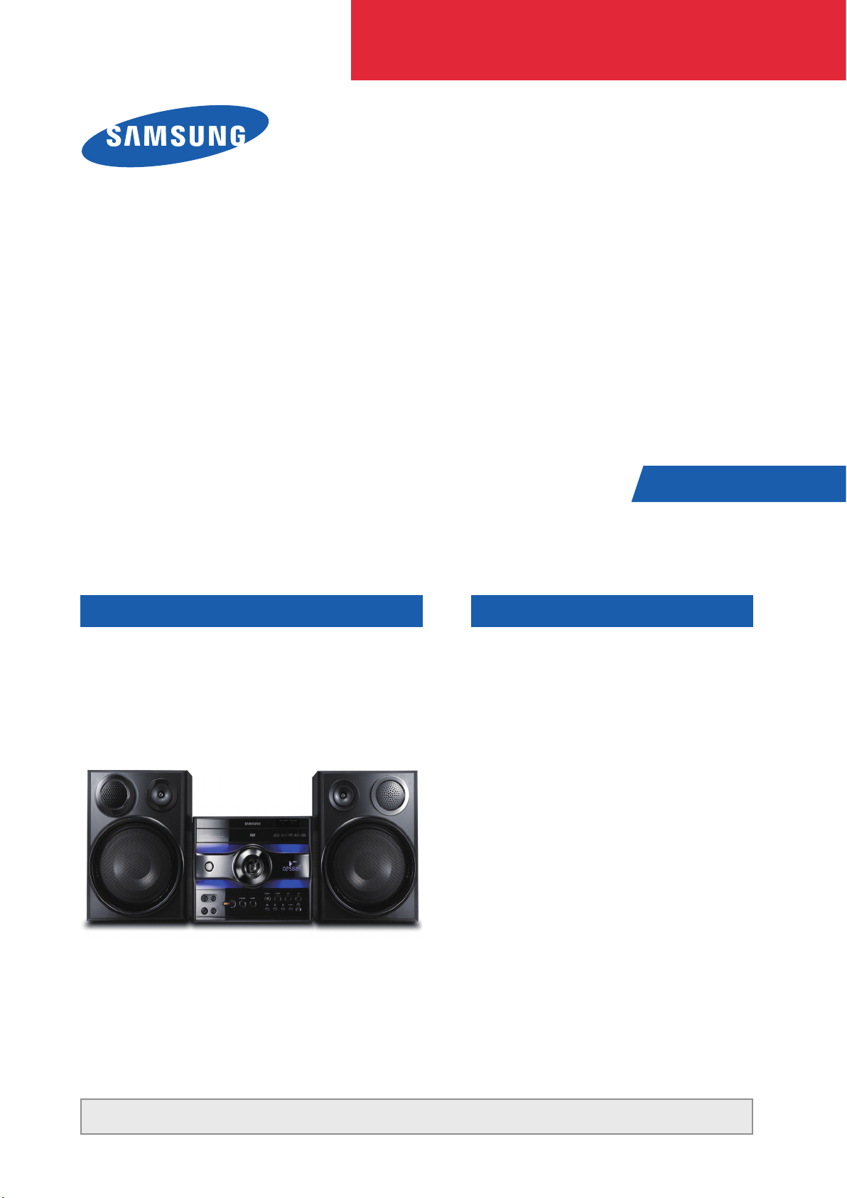
MAX-G55
CONTENTS
Refer to the service manual in the GSPN (see the rear cover) for the more information.
Page 2
GSPN (Global Service Partner Network)
Area Web Site
North America service.samsungportal.com
Latin America latin.samsungportal.com
CIS cis.samsungportal.com
Europe europe.samsungportal.com
China china.samsungportal.com
Asia asia.samsungportal.com
Mideast & Africa mea.samsungportal.com
This Service Manual is a property of Samsung Electronics
Co.,Ltd. Any unauthorized use of Manual can be punished
under applicable International and/or domestic law.
© Samsung Electronics Co.,Ltd.
Printed in Korea
May. 2009
Page 3

Contents
1. Precaution
1-1 Safety Precautions ...........................................................................................1-1
1-2 Servicing Precautions ......................................................................................
1-3 Precautions for Electrostatically Sensitive Devices (ESDs) .............................
2. Product Specification
2-1 Product Feature ...............................................................................................2-1
2-2 Specifications ...................................................................................................
2-3 Specifications Analysis .....................................................................................
2-4 Accessories ......................................................................................................
3. Disassembly & Reassembly
3-1 Overall Disassembly & Reassembly ................................................................3-1
1-3
1-4
2-4
2-7
2-9
4. Troubleshooting
4-1 Checkpoints by Error Mode.............................................................................. 4-2
4-2 MICOM, MPEG Initialization & Update ............................................................
5. Exploded View & Part List
5-1 Exploded View .................................................................................................5-2
5-2 Speaker System ...............................................................................................5-4
5-3 Electrical Part List ............................................................................................5-5
6. PCB Diagram
6-1 Wiring Diagram ................................................................................................6-2
6-2 FRONT PCB Top ..............................................................................................
6-3 FRONT PCB Bottom ........................................................................................
6-4 MAIN PCB Top .................................................................................................
6-5 MAIN PCB Bottom ...........................................................................................
6-6 MPEG PCB Top ...............................................................................................
6-7 MPEG PCB Bottom ..........................................................................................
4-11
6-3
6-5
6-6
6-8
6-10
6-13
Page 4

Contents
7. Schematic Diagram
7-1 Overall Block Diagram .....................................................................................7-2
7-2 FRONT .............................................................................................................
7-3 MAIN ................................................................................................................
7-4 AMP .................................................................................................................
7-5 USB/MIC, MPEG Power ..................................................................................
7-6 MPEG
7-3
7-4
7-5
7-6
...............................................................................................................7-7
Page 5
Precaution
1. Precaution
Follow these safety, servicing and ESD precautions to prevent damage and protect against potential hazards such
as electrical shock and X-rays.
1-1 Safety Precautions
1. Be sure that all of the built-in protective devices are replaced.
2. When reinstalling the chassis and its assemblies, be sure to restore all protective devices, including control
knobs and compartment covers.
3. Make sure that there are no cabinet openings through which people--particularly children--might insert fingers
and contact dangerous voltages. Such openings include the spacing between the picture tube and the cabinet
mask, excessively wide cabinet ventilation slots, and improperly fitted back covers.
4. Design Alteration Warning:
Never alter or add to the mechanical or electrical design of the unit.
Example: Do not add auxiliary audio or video connectors. Such alterations might create a safety hazard.
Also, any design changes or additions will void the manufacturer’s warranty.
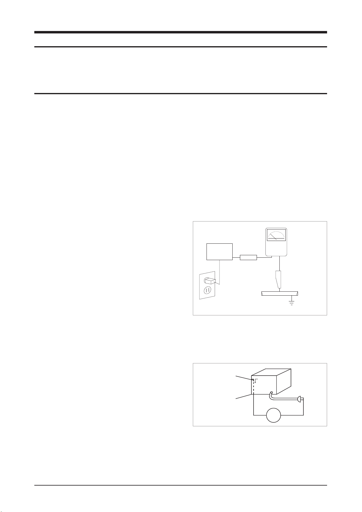
5. Leakage Current Hot Check (Fig. 1-1):
Warning: Do not use an isolation transformer during this
test. Use a leakage-current tester or a metering system
that complies with American National Standards Institute
(ANSI C101.1, Leakage Current for Appliances), and
Underwriters Laboratories (UL Publication UL1410,
59.7).
With the unit completely reassembled, plug the AC line
cord directly into a 120V AC outlet. With the unit’s AC
switch first in the ON position and then OFF, measure
the current between a known earth ground (metal water
DEVICE
UNDER
TEST
TEST ALL
EXPOSED METAL
SURFACES
2-WIRE CORD
ALSO TEST WITH
PLUG REVERSED
(USING AC
ADAPTER PLUG
AS REQUIRED)
<Fig. 1-1 AC Leakage Test>
LEAKAGE
CURRENT
TESTER
(READING
SHOULD NOT BE
ABOVE 0.5mA)
EARTH
GROUND
pipe, etc.) and all exposed metal parts. Examples:
Handle brackets, metal cabinets, screwheads and control shafts. The current measured should not exceed 0.5
milliamp. Reverse the powerplug prongs in the AC outlet and repeat.
6. Insulation Resistance Cold Check:
(1) With the unit’s AC plug disconnected from the AC
source, connect an electrical jumper across the two AC
Antenna
Terminal
prongs. (2) Set the power switch to ON. (3) Measure
the resistance between the shorted AC plug and any
exposed metallic parts.
Example: Screwheads, antenna, control shafts or handle
brackets.
Exposed
Metal Part
ohm
Ohmmeter
<Fig. 1-2 Insulation Resistance Test>
If any of the exposed metallic parts has a return path
to the chassis, the measured resistance should be between 1 and 5.2 megohms. If there is no return path, the
measured resistance should be “infinite.” If the resistance is outside these limits, a shock hazard might exist.
See Fig. 1-2.
Samsung Electronics 1-1
Page 6

1-2 Samsung Electronics
Precaution
7. Components, parts and wiring that appear to have overheated or that are otherwise damaged should be
replaced with parts that meet the original specifications. Always determine the cause of damage or overheating,
and correct any potential hazards.
8. Observe the original lead dress, especially near the following areas: Antenna wiring, sharp edges, and
especially the AC and high voltage power supplies. Always inspect for pinched, out-of-place, or frayed wiring.
Do not change the spacing between components and the printed circuit board. Check the AC power cord for
damage. Make sure that no wires or components touch thermally hot parts.
9. Product Safety Notice:
Some electrical and mechanical parts have special safety-related characteristics which might not be obvious
from visual inspection. These safety features and the protection they give might be lost if the replacement
component differs from the original--even if the replacement is rated for higher voltage, wattage, etc.
10. Components that are critical for safety are indicated in the circuit diagram by shading,
or . Use
replacement components that have the same ratings, especially for flame resistance and dielectric strength
specifications. A replacement part that does not have the same safety characteristics as the original might
create shock, fire or other hazards.
Page 7
Precaution
1-2 Servicing Precautions
1. Servicing precautions are printed on the cabinet. Follow them.
2. Always unplug the unit’s AC power cord from the AC power source before attempting to: (a) Remove or reinstall
any component or assembly, (b) Disconnect an electrical plug or connector, (c) Connect a test component in
parallel with an electrolytic capacitor.
3. Some components are raised above the printed circuit board for safety. An insulation tube or tape is sometimes
used. The internal wiring may be clamped to prevent contact with thermally hot components. Reinstall all such
elements to their original position.
4. After servicing, always check that the screws, components and wiring have been correctly reinstalled.
Make sure that the portion around the serviced part has not been damaged.
5. Check the insulation between the blades of the AC plug and accessible conductive parts (examples: metal
panels, input terminals and earphone jacks).
6. Insulation Checking Procedure: Disconnect the power cord from the AC source and turn the power switch ON.
Connect an insulation resistance meter (500V) to the blades of the AC plug.
The insulation resistance between each blade of the AC plug and accessible conductive parts (see above)
should be greater than 1 megohm.
7. Never defeat any of the B+ voltage interlocks. Do not apply AC power to the unit (or any of its assemblies)
unless all solid-state heat sinks are correctly installed.
8. Always connect a test instrument’s ground lead to the instrument chassis ground before connecting the positive
lead; always remove the instrument’s ground lead last.
First read the “Safety Precautions” section of this manual. If some unforeseen circumstance
creates a conflict between the servicing and safety precautions, always follow the safety
precautions.
Samsung Electronics 1-3
Page 8

Precaution
1-3 Precautions for Electrostatically Sensitive Devices (ESDs)
1. Some semiconductor (“solid state”) devices are easily damaged by static electricity.
Such components are called Electrostatically Sensitive Devices (ESDs). Examples include integrated circuits
and some field-effect transistors. The following techniques will reduce the occurrence of component damage
caused by static electricity.
2. Immediately before handling any semiconductor components or assemblies, drain the electrostatic charge from
your body by touching a known earth ground. Alternatively, wear a discharging wrist-strap device. (Be sure to
remove it prior to applying power--this is an electric shock precaution.)
3. After removing an ESD-equipped assembly, place it on a conductive surface such as aluminum foil to prevent
accumulation of electrostatic charge.
4. Do not use freon-propelled chemicals. These can generate electrical charges that damage ESDs.
5. Use only a grounded-tip soldering iron when soldering or unsoldering ESDs.
6. Use only an anti-static solder removal device. Many solder removal devices are not rated as “anti-static” (these
can accumulate sufficient electrical charge to damage ESDs).
7. Do not remove a replacement ESD from its protective package until you are ready to install it.
Most replacement ESDs are packaged with leads that are electrically shorted together by conductive foam,
aluminum foil or other conductive materials.
8. Immediately before removing the protective material from the leads of a replacement ESD, touch the protective
material to the chassis or circuit assembly into which the device will be installed.
9. Minimize body motions when handing unpackaged replacement ESDs. Motions such as brushing clothes
together, or lifting a foot from a carpeted floor can generate enough static electricity to damage an ESD.
1-4 Samsung Electronics
Page 9

2. Product Specification
2-1 Product Feature
2-1-1 MAX-DG56 Product Feature
Power
• 2.1ch: 280W Total RMS / 3,100W PMPO (Front: 90W/ch, S/W: 100W)
• EQ: 6 Mode
Special Functions
• CD Ripping (1x, 192 Kbps)
• Party Mode: Superb Sound + Flash LED Light
Connectivity
• USB Host (Divx, MP3, JPEG)
• Portable Audio In (3.5 phi Stereo Jack)
Product Specification
Disc
• Type: 3 Roulette
• Compatible: DVD, Divx, MP3, CD/CD-R/CD-RW, WMA, VCD (Regional Option)
In/Out: Component, Composite, Audio L-R
2-1-2 MAX-G56 Product Feature
Power
• 2.1ch: 280W Total RMS / 3,100W PMPO (Front: 90W/ch, S/W: 100W)
• EQ: 6 Mode
Special Functions
• CD Ripping (1x, 192 Kbps)
• Party Mode: Superb Sound + Flash LED Light
Connectivity
• USB Host (MP3)
• Portable Audio In (3.5 phi Stereo Jack)
Disc
• Type: 3 Roulette
• Compatible: MP3, CD-R/CD-RW, WMA
Samsung Electronics 2-1
Page 10

Product Specification
2-1-3 MAX-G55 Product Feature
Power
• 2ch: 180W Total RMS / 2,000W PMPO (Front: 90W/ch)
• EQ: 6 Mode
Special Functions
• CD Ripping (1x, 192 Kbps)
• Party Mode: Superb Sound + Flash LED Light
Connectivity
• USB Host (MP3)
• Portable Audio In (3.5 phi Stereo Jack)
Disc
• Type: 3 Roulette
• Compatible: CD-R/CD-RW, WMA
2-1-4 MAX-DG54 Product Feature
Power
• 2.1ch: 280W Total RMS / 3,100W PMPO (Front: 90W/ch, S/W: 100W)
• EQ: 6 Mode
Special Functions
• CD Ripping (1x, 192 Kbps)
• Party Mode: Superb Sound + Flash LED Light
Connectivity
• USB Host (Divx, MP3, JPEG)
• Portable Audio In (3.5 phi Stereo Jack)
Disc
• Type: 3 Roulette
• Compatible: DVD, Divx, MP3, CD/CD-R/CD-RW, WMA, VCD (Regional Option)
In/Out: Component, Composite, Audio L-R
2 Tape Deck
2-2 Samsung Electronics
Page 11

2-1-5 MAX-DG53 Product Feature
Power
• 2ch: 180W Total RMS / 2,000W PMPO (Front: 90W/ch)
• EQ: 6 Mode
Special Functions
• CD Ripping (1x, 192 Kbps)
• Party Mode: Superb Sound + Flash LED Light
Connectivity
• USB Host (Divx, MP3, JPEG)
• Portable Audio In (3.5 phi Stereo Jack)
Disc
• Type: 3 Roulette
• Compatible: CD-R/CD-RW, WMA
Product Specification
Disc
• Type: 3 Roulette
• Compatible: DVD, Divx, MP3, CD/CD-R/CD-RW, WMA, VCD (Regional Option)
In/Out: Component, Composite, Audio L-R
2 Tape Deck
Samsung Electronics 2-3
Page 12
Product Specification
2-2 Specifications
2-2-1
MAX-DG56 Specications
Basic Specification
Signal/noise ratio
RADIO FM
COMPACT
DISC
PLAYER
AMPLIFIER
Output Power
Usable sensitivity
Total harmonic
distortion
Capacity 3 discs
Frequency range
Signal/noise ratio
Distortion 0.05 % (at 1 KHz)
Channel separation
Disc sizes
Front Speaker (6Ω) 90 Watts/CH RMS, IEC (total harmonic distortion: 10 %)
Subwoofer Speaker (6Ω) 100 Watts/CH RMS, IEC (total harmonic distortion: 10 %)
Channel separation
62 dB
10 dB
0.3 %
20 Hz - 20 KHz (± 3 dB)
90 dB (at 1 KHz) with filter
75 dB
Diameter: 120 or 80 mm. Thickness: 1.2 mm
40 dB
GENERAL
Signal/noise ratio
Power Consumption
Dimensions 377 (W) x 227 (H) x 270 (D) mm
75 dB
40W
2-4 Samsung Electronics
Page 13
Product Specification
2-2-2
MAX-G56 / MAX-G55 Specications
Basic Specification
Signal/noise ratio
RADIO FM
COMPACT
DISC
PLAYER
AMPLIFIER
Output Power
Usable sensitivity
Total harmonic
distortion
Capacity 3 discs
Frequency range
Signal/noise ratio
Distortion 0.05 % (at 1 KHz)
Channel separation
Disc sizes
Front Speaker (6Ω) 90 Watts/CH RMS, IEC (total harmonic distortion: 10 %)
Subwoofer Speaker (6Ω) 100 Watts/CH RMS, IEC (total harmonic distortion: 10 %)
Channel separation
62 dB
10 dB
0.3 %
20 Hz - 20 KHz (± 1 dB)
90 dB (at 1 KHz) with filter
75 dB
Diameter: 120 or 80 mm. Thickness: 1.2 mm
45 dB
GENERAL
Signal/noise ratio
Power Consumption
Dimensions 270 (W) x 227 (H) x 377 (D) mm
75 dB
50W
Samsung Electronics 2-5
Page 14
Product Specification
2-2-3
MAX-DG54 / MAX-DG53 Specications
Basic Specification
Signal/noise ratio
RADIO FM
COMPACT
DISC
PLAYER
AMPLIFIER
Output Power
Usable sensitivity
Total harmonic
distortion
Capacity 3 discs
Frequency range
Signal/noise ratio
Distortion 0.1 % (at 1 KHz)
Channel separation
Disc sizes
Front Speaker (6Ω)
Subwoofer Speaker (6Ω)
62 dB
10 dB
0.4 %
20 Hz - 20 KHz (± 3 dB)
90 dB (at 1 KHz) with filter
75 dB
Diameter: 120 or 80 mm. Thickness: 1.2 mm
90 Watts/CH RMS, IEC (total harmonic distortion: 10 %)
(MAX-DG54/DG53)
100 Watts/CH RMS, IEC (total harmonic distortion: 10 %)
(MAX-DG54)
GENERAL
Channel separation
Signal/noise ratio
Power Consumption
Dimensions 377 (D) x 227 (H) x 270 (W) mm
60 dB
70 dB
50 W
2-6 Samsung Electronics
Page 15
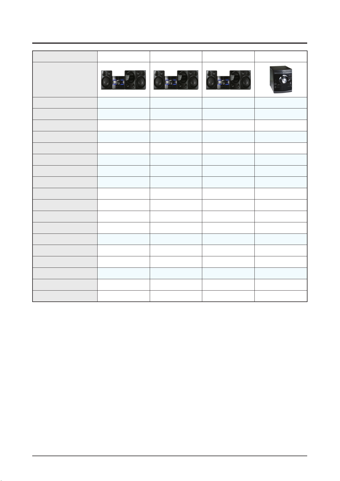
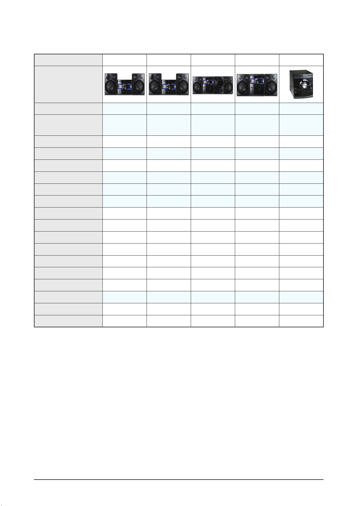
2-3 Specifications Analysis
Product Specification
Model Name MAX-KG56 MAX-DG56 MAX-G56
Photo
RMS 280W 280W 280W
Output Power
Front Display
Party Mode
DIMMER
CD/DVD DVD DVD CD
TAPE X X X
USB HOST
CD RIPPING
EQ/DSP 8 8 8
Audio In
90W x 2 + 100W 90W x 2 + 100W 90W x 2 + 100W
VFD VFD VFD
VIDEO/AUDIO VIDEO/AUDIO AUDIO
MAX-DA55
180W
90W x 2
VFD
X
DVD
AUDIO
8
HEADPHONE/MIC
Karaoke
FM
Tuner Memory
Remote Key
Dual Voltage
SPK Impedance
20 20 20
60 Key 60 Key 40 Key
4Ω 4Ω 4Ω
X X
: application, X: non-application
X
20
57 Key
4Ω
Samsung Electronics 2-7
Page 16
Product Specification
Model Name MAX-DG55 MAX-G55 MAX-DG54 MAX-DG53
Photo
RMS 180W 180W 280W 180W
Output Power
Front Display
Party Mode
DIMMER
90W x 2 90W x 2
VFD VFD VFD VFD
90W x 2 +
100W
90W x 2
CD/DVD DVD CD DVD DVD
TAPE X X
USB HOST
CD RIPPING
VIDEO/AUDIO AUDIO VIDEO/AUDIO VIDEO/AUDIO
EQ/DSP 8 8 8 8
MAX-DA55
180W
90W x 2
VFD
X
DVD
AUDIO
8
Audio In
HEADPHONE/MIC
Karaoke X X X X
FM
Tuner Memory
Remote Key
Dual Voltage
SPK Impedance
20 20 20 20
40 Key 40 Key 40 Key 40 Key
4Ω 4Ω 4Ω 4Ω
X
20
57 Key
4Ω
: application, X: non-application
2-8 Samsung Electronics
Page 17
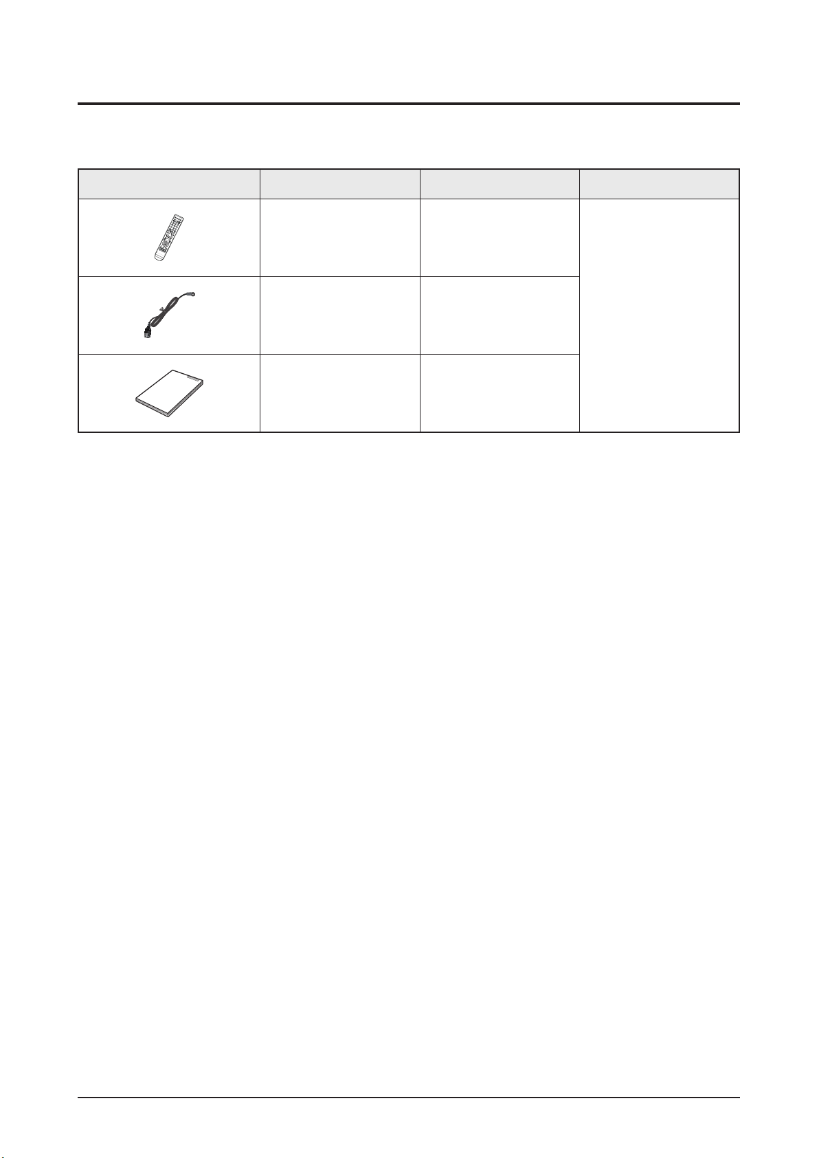
2-4 Accessories
2-4-1 Supplied Accessories
Accessories Item Item code Remark
Product Specification
Remote Control
FM Antenna
User's Manual
AH59-02147A
AH42-00021A
AH68-02162F
AH68-02162G
AH68-02162H
Samsung Service
Center
Samsung Electronics 2-9
Page 18

MEMO
2-10 Samsung Electronics
Page 19
Disassembly & Reassembly
3. Disassembly & Reassembly
3-1 Overall Disassembly & Reassembly
- Be careful to follow the disassembly sequence described in the manual. Otherwise, the product
may be damaged.
- Be sure to carefully read and understand the safety instructions before performing any work as
the IC chips on the PCB are vulnerable to static electricity.
- Assemble in the reverse order of disassembly.
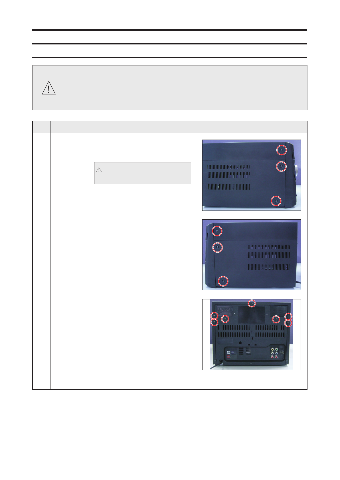
No. Part Name Description Description Photo
1 COVER-
SIDE-L
/
COVER-
SIDE-R
/
CABINET-
REAR
1) Unfasten 15 screws.
: BH,3*10,BLACK
Be careful not to make any
scratches as you remove it.
<MAX-DG56 CABINET-REAR>
Samsung Electronics 3-1
Page 20
Disassembly & Reassembly
No. Part Name Description Description Photo
1 COVER-
SIDE-L
/
COVER-
SIDE-R
/
CABINET-
REAR
<MAX-G55 CABINET-REAR>
<MAX-G56/DG55 CABINET-REAR>
<MAX-DG54/DG53 CABINET-REAR>
3-2 Samsung Electronics
Page 21

Disassembly & Reassembly
No. Part Name Description Description Photo
2 CABINET-
TOP
1) Pull up and remove the CABINET-
TOP.
/
DOOR-CD
2) Power on and open the disk,
separate DOOR-CD.
3 CD-DECK 1) Pull up and remove the CD-DECK.
4 MPEG PCB
(MAX-DG5x
Only)
1) Unfasten the 3 screws and remove
MPEG PCB.
: BH 2.6*8 WHITE
Samsung Electronics 3-3
Page 22

Disassembly & Reassembly
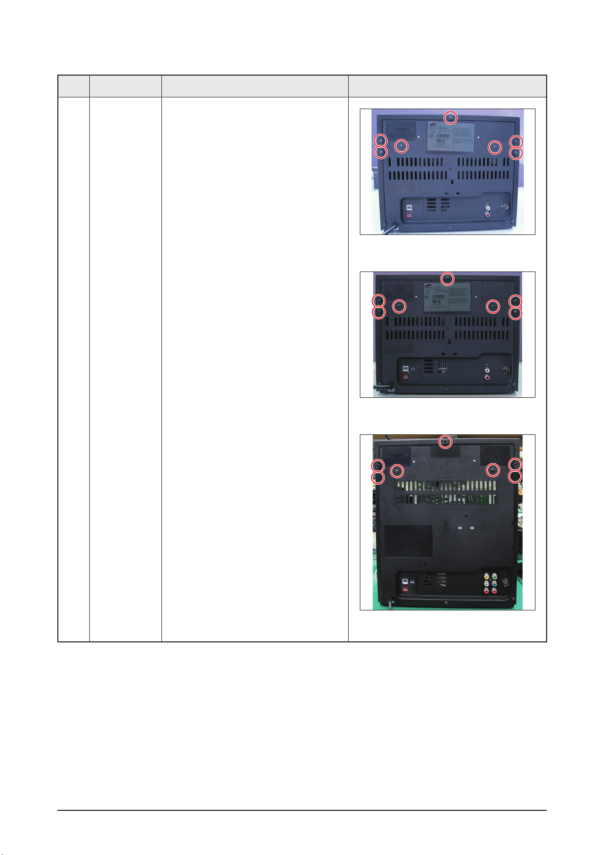
No. Part Name Description Description Photo
5 CABINET-
REAR
1) Unfasten the 6 screws and remove
CABINET-REAR.
: BH,3*10,BLACK
<MAX-DG56 CABINET-REAR>
<MAX-G55 CABINET-REAR>
<MAX--G56/DG55 CABINET-REAR>
<MAX-DG54/DG53 CABINET-REAR>
3-4 Samsung Electronics
Page 23

Disassembly & Reassembly
No. Part Name Description Description Photo
6 MAIN PCB 1) Unfasten 8 screws on the MAIN-PCB.
: BH,3*10,WHITE
7 CABINET
BOTTOM
1) Unfasten the 2 screws.
: BH,3*10,black
Samsung Electronics 3-5
Page 24

Disassembly & Reassembly
No. Part Name Description Description Photo
8 ASSY-
FRONT
/
TAPE DECK
1) Pull the hook at
separate ASSY-FRONT.
2) (MAX-DG54/DG53 Only)
4 screws to disasemble tape deck.
: BH 3*10 BLACK
1 and 2 of and
1
2
<MAX-DG54/DG53 TAPE-DECK>
3) Unfasten 11 screws.
: BH 3*10 BLACK
<MAX-DG56/G56/DG55/G55 ASSY FRONT>
<MAX-DG54/DG53 ASSY FRONT>
3-6 Samsung Electronics
Page 25

Troubleshooting
4. Troubleshooting
4-1 Checkpoints by Error Mode ................................................................4-2
4-2 MICOM, MPEG Initialization & Update ................................................
4-11
Samsung Electronics 4-1
Page 26

Troubleshooting
4-1 Checkpoints by Error Mode
4-1-1 No Power
No Power
Refer to wave pattern
image of Fig. 4-1.
1
Check MAIN PCB UIC1
Pin 14, 40, 55 and
89: 5V
Yes
Check MAIN PCB
UIC1 Pin 3: 5V (High)
Yes
Check VFD Voltage
in MAIN PCB FCN1
Pin 26, 27, 28.
No
No
No
Check MAIN PCB
IC1P102 Pin 3: 5.6V
Yes
Check MAIN PCB
Q1P110 Pin 3: High
Check or replace
PT02 (VFD+: Pin 6,
VFD-: Pin 7, -VP: Pin 10)
No
Replace IC1P101
(1203-004520)
No
Check POWER_ON
Signal Line
Yes
2
Check reset circuit in
MAIN PCB X-TAL1, UQ1
part ok?
Yes
Refer to wave pattern
image of Fig. 4-2.
Replace MICOM IC
No
Replace X-TAL1, UQ1 parts
4-2 Samsung Electronics
Page 27

UIC1
1
Troubleshooting
1
1
1
1
MAIN, page 7-4
1
1
1
1
MAIN PCB Bottom, page 6-8
<Fig. 4-1>
Samsung Electronics 4-3
Page 28

Troubleshooting
FIC1
DCN1
UIC1
2
MAIN, page 7-4
2
2
MAIN PCB Bottom, page 6-8
<Fig. 4-2>
4-4 Samsung Electronics
Page 29

4-1-2 No Output
Troubleshooting
No Output
Check all function
(CD/DVD, Tuner, AUX).
Yes
All function fail
Check MAIN PCB
FIC1 R2S15904 input and
output signal
Yes
Input fine but output fail
1 / 2
Check MAIN PCB
AAIC1 Pin 23: Low Mute; High Normal
FIC1 Pin 24: 9V
Yes
Refer to wave pattern
image of Fig. 4-3-1
and Fig. 4-3-2.
No
Only CD/DVD/USB
No
Input signal fail
No
Check MPEG PCB
Check AUX signal input and signal
pattern
Check MICOM IC "UIC1"
Pin 44: Low Normal, High Mute
Check MAIN PCB
PT01 Pin 9: -24V and
Pin 11: +24V
Yes
Replace AAIC1 (L/R),
AAIC2 (Subwoofer)
No
Check SMPS stage
(All power source check)
Samsung Electronics 4-5
Page 30

Troubleshooting
AAIC1
AAIC2
1
1
AMP, page 7-5
1
MAIN PCB Top, page 6-6
<Fig. 4-3-1>
4-6 Samsung Electronics
Page 31

FIC1
2
Troubleshooting
MAIN, page 7-4
2
2
MAIN PCB Bottom, page 6-8
<Fig. 4-3-2>
Samsung Electronics 4-7
Page 32

Troubleshooting
4-1-3 CD/DVD PACK
Disc can not play
1
Check 27MHz
crystal of MX1
Refer to wave pattern
Yes
Check voltage DCN2
in MAIN PCB
(3.3V, 8V, 5V)
NoNo
image of Fig. 4-4.
TV display LOGO ok?
Yes
Press “Eject” button,
if Disc can Eject?
Yes
“NO DISC” after
Loading a long time?
No
No
No
Check reset voltage
at Pin 52 of MIC1
Yes
Check DCN1 Pin 18
(MRST)
Check MECHA 9P
Flat Cable
Check Pick up Lens
and Pick up Flat Cable
No
Yes
Check MIC1 ZR36966
Check Servo Parts
2
Check DCN1 Pin 19,
20, 21 and 22
Refer to wave pattern
image of Fig. 4-5.
4-8 Samsung Electronics
Page 33

Troubleshooting
RFCON1
MACON1
DIC2
ACCON1
DAIC1
OPIC1
PIC1
MIC2
DIC1
MIC1
MIC3C
MIC3D
BIC1
IOCON
1
1
1
MPEG, page 7-7
MPEG PCB Top, page 6-10
<Fig. 4-4>
Samsung Electronics 4-9
Page 34

Troubleshooting
DCN1
2
MAIN, page 7-4
2
2
MAIN PCB Top, page 6-6
<Fig. 4-5>
4-10 Samsung Electronics
Page 35

4-2 MICOM, MPEG Initialization & Update
MICOM Initial
In STANDBY condition, press “STOP” button of Main Unit 5 seconds more, time display as ‘--:--’.
Then Initialization complete.
MICOM Update
MICOM update is enabled via USB and CD/DVD.
1. Copy MICOM update file to CD/DVD/USB.
2. File name is “micom.ssp”, “update.ver”.
Troubleshooting
3. DVD Model: Osd shows update screen. You have to make sure your update file is most recently version.
Then press “ENTER” to proceed.
CD Model: VFD shows “reading”. And “update” shows up and blinking. Wait until MAIN set automatically power
off.
MPEG Update
1. Copy MPEG update file to CD/DVD/USB.
2. File name is “DCMCXXXW.bin”
3. DVD Model: Osd shows update screen. You have to make sure your update file is most recently version.
Then press “ENTER” to proceed.
CD Model: VFD shows “reading”. And “update” shows up and blinking. Wait until MAIN set automatically power
off.
Samsung Electronics 4-11
Page 36

MEMO
4-12 Samsung Electronics
Page 37

Exploded View & Part List
5. Exploded View & Part List
5-1 Exploded View ......................................................................................5-2
5-2 Speaker System....................................................................................5-4
5-3 Electrical Part List ................................................................................5-5
Samsung Electronics 5-1
This Document can not be used without Samsung’s authorization.
Page 38

5-2 Samsung Electronics
Exploded View & Part List
This Document can not be used without Samsung’s authorization.
AK111
AD150
T0023
T0003
M0007
T0245
T0002
C015
C942
AC510
AC510
AA302
AA304
C982
AD501
AL501
AC503
WA003
C001
APDC1
P005
M0014
T0268
W384
W384
W004
W391
W391
AC510
W391
LD61A
W391
W391
AC502
W391
W391
W391
5-1 Exploded View
S.N.A: Service Not Available
Page 39

Exploded View & Part List
Part List
Loc. No. Part No. Description;Specification Q’ty SNA Remark
AA302 AH97-03190A ASSY DOOR-CD;MAX-G55,MAX-G55,EXP,- 1 SNA
AA304 AH97-03038A ASSY KNOB-VOL;MAX-G55,MAX-G55,EXP,- 1 SNA
AC502 AH63-01818A COVER-SIDE-L;MAX-G55,HIPS,20,243 1 SNA
AC503 AH63-01819A COVER-SIDE-R;MAX-G55,HIPS,20,243 1 SNA
AC510 3708-000411 CONNECTOR-FPC/FFC/PIC;12P,1.25mm,STRAIGH 1 SA
AC510 3708-001761 CONNECTOR-FPC/FFC/PIC;28P,1mm,STRAIGHT,S 1 SNA
AC510 3708-001577 CONNECTOR-FPC/FFC/PIC;30P,1.25mm,STRAIGH 1 SA
AD150 AH64-04850D DECORATION-FRONT;MAX-G55,ABS+PMMA,54.4,2 1 SNA
AD501 AH64-04848A DECORATION-DISPLAY;MAX-G55,PMMA SMOKE,93 1 SNA
AK111 AH64-04846A KNOB-DISK;MAX-G55,ABS,11,56 1 SNA
AL501 AH67-00533A LENS-REFLECTOR_UPPER;MAX-G55,PMMA,L242*W 2 SNA
APDC1 AH92-02965B ASSY PCB DECK-CD;AH,G55,CD,MPEG PCB ASSY 1 SNA
C001 AH97-03036A ASSY CABINET-FRONT;MAX-G55,MAX-G55,EXP,- 1 SNA
C015 AH64-05139A CABINET-TOP;MAX-G55,HIPS,270,330,BLACK,E 1 SNA
C942 AH64-04874A CABINET-REAR;MAX-G55,HIPS,220,265 1 SNA
C982 AH64-04864A KNOB-MIC-VOL;MAX-G55,ABS,13,17 1 SNA
LD61A AH61-02804A HOLDER-LED;MAX-G55,HIPS,240,85,EXP 1 SNA
M0007 AH64-04845A KNOB-FUNCTION;MAX-G55,ABS,42,177 1 SNA
M0014 AH92-03023G ASSY PCB MAIN;MAIN PCB ASSY,MAX-G55,EUR, 1 SA
P005 AH94-02245C ASSY PCB FRONT;FRONT PCB ASSY,MAX-G56R/E 1 SNA
T0002 AH64-04873A CABINET-BOTTOM;MAX-G55,SECC 0.8,262,298 1 SNA
T0003 AH64-04844A CABINET-FRONT;MAX-G55,HIPS,264,226 1 SNA
T0023 AH64-04847A KNOB-POWER;MAX-G55,ABS,28,28 1 SNA
T0245 AH61-02903A HOLDER-PCB;MAX-G55,ABS,25,40,BLK 1 SNA
T0268 AC39-10019A CBF-POWER CORD;KKP-419C,H03VVH2-F,VDE/KE 1 SA
W004 6003-000283 SCREW-TAPTYPE;BH,+,-,B,M3,L8,ZPC(WHT),SW 10 SA
W384 6002-000126 SCREW-TAPPING;FH,+,-,2S,M3,L10,ZPC(BLK), 2 SA
W391 6003-000275 SCREW-TAPTYPE;BH,+,B,M3,L10,ZPC(BLK),SWR 40 SA
WA003 AH66-00303A WIRE-CLAMP;MAX-G55,NYLON,L24,BLK 1 SNA
Samsung Electronics 5-3
This Document can not be used without Samsung’s authorization.
Page 40

5-4 Samsung Electronics
Exploded View & Part List
This Document can not be used without Samsung’s authorization.
L
R
FRONT
FRONT
R
L
SPEAKERS OUT
IMPEDANCE 4Ω
5-2 Speaker System
Speaker (L)
Front
Front
Speaker (R)
Part List
Loc. No. Code No. Description;Specification Q’ty SNA Remark
Front Speaker (L) AH81-04703A SPEAKER; PS-G55,SPEAKER SYSTEM _L-,-,-,-,- 1 SA
Front Speaker (R) AH81-04702A SPEAKER; PS-G55,SPEAKER SYSTEM _R,-,-,-,-,- 1 SA
Page 41

Exploded View & Part List
5-3 Electrical Part List
Loc. No. Part No. Description;Specification Q’ty SNA Remark Loc. No. Part No. Description;Specification Q’ty SNA Remark
APDC1 AH92-02965B ASSY PCB DECK-CD;AH,G55,CD,MPEG PCB 1 SNA
AAC14 2203-000888 C-CER,CHIP;4.7nF,10%,50V,X7R,TP,160 2 SNA
AC109 2203-000783 C-CER,CHIP;0.33nF,5%,50V,C0G,1608 2 SNA
AC14 2402-000136 C-AL,SMD;22uF,20%,16V,GP,TP,5.3x5.3 2 SNA
AC510 3708-000411 CONNECTOR-FPC/FFC/PIC;12P,1.25mm,ST 1 SA
AC510 3708-001761 CONNECTOR-FPC/FFC/PIC;28P,1mm,STRAI 1 SNA
AC510 3708-002272 CONNECTOR-FPC/FFC/PIC;4P,1mm,ANGLE, 1 SNA
AC6 2402-001049 C-AL,SMD;10uF,20%,16V,GP,TP,3.3x3.3 4 SA
AD1 0407-000116 DIODE-SWITCHING;KDS181,DAP202K,SDS2 1 SNA
AIC1 1002-001294 IC-D/A CONVERTER;PCM1742KE,24BIT,TS 1 SNA
AL1 2703-000275 INDUCTOR-SMD;33UH,10%,2012 1 SA
AR02 2007-000125 R-CHIP;3.9Kohm,5%,1/10W,TP,1608 2 SNA
AR108 2007-000097 R-CHIP;47Kohm,5%,1/10W,TP,1608 4 SNA
AR150 2007-000078 R-CHIP;1Kohm,5%,1/10W,TP,1608 8 SNA
AR30 2007-000074 R-CHIP;100ohm,5%,1/10W,TP,1608 22 SNA
C0104 3809-000169 CABLE-FLAT;30V,80C,150mm,12P,1.25mm 1 SA
C0104 3809-002254 CABLE-FLAT;30V,80C,190mm,28P,1.0mm, 1 SNA
C125 2203-006361 C-CER,CHIP;10000nF,10%,10V,X5R,TP,2 20 SNA
C134 2203-000257 C-CER,CHIP;10nF,10%,50V,X7R,TP,1608 2 SNA
C212 2203-000440 C-CER,CHIP;1nF,10%,50V,X7R,1608 4 SNA
CER04 2007-000084 R-CHIP;4.7Kohm,5%,1/10W,TP,1608 11 SNA
CN1 3708-000491 CONNECTOR-FPC/FFC/PIC;23P,1mm,STRAI 1 SNA
CON-FF 3708-001955 CONNECTOR-FPC/FFC/PIC;8P,1mm,ANGLE, 1 SA
DR1 2007-000023 R-CHIP;120ohm,5%,1/8W,TP,2012 1 SNA
DR1 2007-000043 R-CHIP;1Kohm,1%,1/10W,TP,1608 2 SNA
DR10 2007-000113 R-CHIP;33ohm,5%,1/10W,TP,1608 5 SNA
FMR4 2007-000080 R-CHIP;2Kohm,5%,1/10W,TP,1608 2 SNA
IC104 0801-002683 IC-CMOS LOGIC;74HCT245,TRANSCEIVER, 1 SA
J914 2007-000029 R-CHIP;0ohm,5%,1/8W,TP,2012 3 SNA
KAR13 2007-000060 R-CHIP;100Kohm,1%,1/10W,TP,1608 5 SNA
KAR21 2007-000070 R-CHIP;0ohm,5%,1/10W,TP,1608 1 SNA
KOP1 1201-000163 IC-OP AMP;4560,SOP,8P,173MIL,DUAL,1 1 SA
KQ1 0501-000279 TR-SMALL SIGNAL;KSA1182-Y,PNP,150mW 2 SA
MIC1 1003-001978 IC-MOTOR DRIVER;AM5766,HSOP28H,28P, 1 SA
MIC3 1107-001600 IC-NOR FLASH;MX25L1605A,16Mbit,2Mx8 1 SNA
MR1 2007-000805 R-CHIP;36Kohm,5%,1/10W,TP,1608 2 SNA
MR13 2007-000092 R-CHIP;15Kohm,5%,1/10W,TP,1608 2 SNA
MR2 2007-000130 R-CHIP;39Kohm,5%,1/10W,TP,1608 1 SNA
MR8 2007-000503 R-CHIP;2.2ohm,5%,1/10W,TP,1608 2 SA
MROP1 2007-000090 R-CHIP;10Kohm,5%,1/10W,TP,1608 2 SNA
MX1 2801-004284 CRYSTAL-SMD;27MHZ,10PPM,28-AAN,20PF 1 SA
MZD1 0403-001411 DIODE-ZENER;5.49-5.73V,200mW,SOD-32 1 SA
ND53F1 1105-001261 IC-DRAM;12L1616A,16,TSOP,50P,400MIL 1 SNA
PIC2 1203-002779 IC-POSI.FIXED REG.;G952T63U,SOT-223 1 SA
PPC2 2203-005148 C-CER,CHIP;100nF,10%,16V,X7R,TP,160 58 SNA
R1 2007-002425 R-CHIP;1ohm,5%,1/10W,TP,1608 2 SNA
R15 2007-000134 R-CHIP;33Kohm,5%,1/10W,TP,1608 1 SNA
R227 2007-000086 R-CHIP;5.6Kohm,5%,1/10W,TP,1608 2 SNA
R329 2007-000081 R-CHIP;2.7Kohm,5%,1/10W,TP,1608 3 SNA
RC34 2203-000280 C-CER,CHIP;0.01nF,0.5pF,50V,C0G,160 2 SNA
RE6 2402-001042 C-AL,SMD;100uF,20%,16V,GP,TP,6.6x6. 3 SNA
REG1 1203-001255 IC-POSI.FIXED REG.;7805,D-PAK,3P,PL 1 SA
RIC3 1003-001508 IC-MOTOR DRIVER;FAN8082DTF,SOP,8P,2 1 SA
RR17 2007-001146 R-CHIP;7.5ohm,5%,1/8W,TP,2012 2 SNA
RR2 2007-000075 R-CHIP;220ohm,5%,1/10W,TP,1608 2 SNA
SD3 0407-000114 DIODE-SWITCHING;KDS184,80V,100mA,SO 1 SA
UR16 2007-000552 R-CHIP;20ohm,5%,1/10W,TP,1608 2 SNA
ZC14 2203-000626 C-CER,CHIP;0.022nF,5%,50V,C0G,1608 1 SNA
ZC165 2203-000815 C-CER,CHIP;0.033nF,5%,50V,C0G,1608 1 SNA
ZC35 2203-000681 C-CER,CHIP;0.027nF,5%,50V,C0G,1608 2 SNA
ZC4 2203-000332 C-CER,CHIP;0.012nF,5%,50V,C0G,1608 2 SNA
ZC52 2203-000669 C-CER,CHIP;27nF,10%,25V,X7R,1608 2 SA
ZR10 2007-001164 R-CHIP;75ohm,1%,1/10W,TP,1608 1 SA
ZR24 2007-000109 R-CHIP;1Mohm,5%,1/10W,TP,1608 1 SNA
ZR37 2007-008567 R-CHIP;15.4Kohm,1%,1/10W,TP,1608 1 SA
ZR45 2007-000329 R-CHIP;11Kohm,5%,1/10W,TP,1608 2 SA
ZR47 2007-007277 R-CHIP;392ohm,1%,1/10W,TP,1608 1 SA
ZRN10 2011-001261 R-NETWORK;33ohm,5%,1/16W,L,CHIP,8P, 1 SA
ZVL3 3301-001495 BEAD-SMD;120ohm,2012,2500mA,TP,115o 10 SA
1204-002955 IC-DECODER;ZR36966PQCG-XE2,TR,128P, 1 SA
2011-001397 R-NETWORK;47Kohm,5%,1/16W,L,CHIP,8P 1 SA
AH41-01184A PCB-DECK;MAX-DG55/G55,FR-4,2.0,0,T1 1 SNA
AH62-00062J HEAT SINK-MPEG;AL,T2.0 1 SNA
AH99-00150A ASSY AUTO INSERT-CD;G55,G55,mpeg,cd 1 SNA
AH97-03070A ASSY-EMPTY MECHA;MAX-DG50,SDM-R32,T 1 SNA
AP090 AH66-00239A PULLEY-BELT;SDM-R31,CR 1.5,75,78,mm 1 SA
AT200 AJ64-00006A LOCKER-TRAY;SDM-R32,POM,WHITE 1 SNA
C539 AH39-00735A WIRE HARNESS;SDM-R31,3P,51MM,3,whit 1 SA
C777 AH63-00360C COVER-BOTTOM;SDM-R31,PS,NTR,CMS-S71 1 SA
CD000 AH61-01509B BASE-MAIN;SDM-R31,ABS,1.5,262,304,N 1 SA
CD220 AH66-00232A GEAR CAM;SDM-R31,POM (20-03),0.8,82 1 SA
CD340 AJ66-00058A LEVER-LIFT;SDM-R32,ABS,BLACK,DVD 1 SNA
CD420 AH73-00025B RUBBER-CD;CMS-D100,BUTYL 5 2 SA
CD520 3409-001171 SWITCH-DETECTOR;5.0,0.1mA ~ 100mA,5 1 SA
CD520 3409-001173 SWITCH-DETECTOR;5.0,0.1~100mA,20gf, 1 SA
FL008 3809-001829 CABLE-FLAT;5.1V,70C,373mm,8P,1mm,UL 1 SNA
H103 AH66-00235A GEAR-PULLEY;SDM-R31,POM (F20-03),0. 1 SA
H108 AH63-00668B TRAY-DISC;SDM-R31,ABS HEAT,1.5,246, 1 SA
H212 AH61-01512B HOLDER-CHUCK;SDM-R31,PC+ABS,1.5,NO 1 SNA
H505 AH63-00669A TRAY-ROULETTE;SDM-R31,ABS 1 SA
MOTOR- 3101-001377 MOTOR-DC;2540RPM,12.6G.CM,5V,120MA 1 SA
SW100 3409-001172 SWITCH-LEVER;5.0,0.1MA ~ 100MA,36de 1 SA
W004 6003-000283 SCREW-TAPTYPE;BH,+,-,B,M3,L8,ZPC(WH 10 SA
W387 6003-001210 SCREW-TAPTYPE;PWH,+,B,M2.6,L6,ZPC(B 8 SA
AH41-00675A PCB-SWITCH;SDM-R31,FR-1,1.6,32.5x37 1 SNA
AH41-00676A PCB-MOTOR;SDM-R31,FR-1,1.6 1 SNA
AH41-01229A FFC-SERVO;SDM-R32,Type=A,PET,4,T0.1 1 SNA
AH41-01230A FFC-P/U;SDM-R32,Type=A,PET,23,T0.12 1 SNA
AH61-02174A HOLDER SPRING-CHUCK;SDM-D1F,SUS 1 SNA
AH61-02179A BODY CLAMPER;SDM-D1F,POM,WHITE 1 SA
AH61-02649A POST-GEAR;SDM-R31,SWRCH18A,9.7,L22. 1 SNA
AH63-01735A SHEET-WASHER;SDM-R31,LUMIPROR,T0.5, 1 SNA
AH66-00230A CAM-SIDE-L;SDM-R31,ABS(HF 380),NTR 1 SA
AH66-00231A CAM-SIDE-R;SDM-R31,ABS (HF-0660I),N 1 SA
AH66-00233A GEAR CAM-MIDDLE;SDM-R31,POM (F20-03 1 SA
AH66-00234A GEAR-PLANET;SDM-R31,POM (F20-03),14 2 SA
AH66-00236A GEAR-SIDE;SDM-R31,POM (F20-03) 2 SA
AH66-00237A LEVER-SIDE;SDM-R31,POM (F20-03) 1 SA
AH66-00238A CAM-SLIDER;SDM-R31,POM (F20-03) 1 SA
AH66-10008A PULLEY-MOTOR;POM,BLK,CMS-CR3 1 SA
AH97-02666A ASSY-TRAVERSE;CMS-S78RB,DVD DECK,FI 1 SNA
Samsung Electronics 5-5
This Document can not be used without Samsung’s authorization.
Page 42

5-6 Samsung Electronics
Exploded View & Part List
Loc. No. Part No. Description;Specification Q’ty SNA Remark Loc. No. Part No. Description;Specification Q’ty SNA Remark
This Document can not be used without Samsung’s authorization.
C 2401-001067 C-AL;3300uF,20%,42V,GP,18x35.5mm,7. 2 SA
C 2401-000480 C-AL;10uF,20%,50V,GP,TP,5x11,5 12 SNA
M0238 AH59-02134D SPEAKER SYSTEM;PS-G55,XAH 1 SNA
T0082 AH81-04702A SPEAKER;PS-G55,SPEAKER SYSTEM _R,-, 1 SNA
T0082 AH81-04705A SPEAKER;PS-G55,CUSHION,-,-,-,-,- 1 SNA
T0082 AH81-04706A SPEAKER;PS-G55,T/W UNIT,-,-,-,-,- 1 SNA
T0082 AH81-04707A SPEAKER;PS-G55,DUCT PAPER,-,-,-,-,- 1 SNA
T0082 AH81-04708A SPEAKER;PS-G55,CABINET,-,-,-,-,- 1 SNA
T0082 AH81-04710A SPEAKER;PS-G55,WOOFER UINT,-,-,-,-, 1 SNA
T0082 AH81-04711A SPEAKER;PS-G55,GRILL WOOFER,-,-,-,- 1 SNA
T0082 AH81-04712A SPEAKER;PS-G55,FRONT PANEL _R,-,-,- 1 SNA
T0082 AH81-04703A SPEAKER;PS-G55,SPEAKER SYSTEM _L,-, 1 SNA
T0082 AH81-04704A SPEAKER;PS-G55,FRONT_PANEL-L,-,-,-, 1 SNA
T0082 AH81-04705A SPEAKER;PS-G55,CUSHION,-,-,-,-,- 1 SNA
T0082 AH81-04706A SPEAKER;PS-G55,T/W UNIT,-,-,-,-,- 1 SNA
T0082 AH81-04707A SPEAKER;PS-G55,DUCT PAPER,-,-,-,-,- 1 SNA
T0082 AH81-04708A SPEAKER;PS-G55,CABINET,-,-,-,-,- 1 SNA
T0082 AH81-04710A SPEAKER;PS-G55,WOOFER UINT,-,-,-,-, 1 SNA
T0082 AH81-04711A SPEAKER;PS-G55,GRILL WOOFER,-,-,-,- 1 SNA
T0082 AH81-04709A SPEAKER;PS-G55,BOX,-,-,-,-,- 1 SNA
M0014 AH92-03023G ASSY PCB MAIN;MAIN PCB ASSY,MAX-G55 1 SA
AAC1 2203-005249 C-CER,CHIP;100nF,10%,50V,X7R,TP,160 9 SNA
AAC14 2203-000888 C-CER,CHIP;4.7nF,10%,50V,X7R,TP,160 2 SNA
AAC17 2203-000595 C-CER,CHIP;0.22nF,5%,50V,C0G,2012 1 SA
AAC22A 2203-002392 C-CER,CHIP;220nF,+80-20%,50V,Y5V,20 7 SA
AAC26A 2203-005218 C-CER,CHIP;470nF,10%,50V,X7R,3216 1 SA
AAC3 2401-001415 C-AL;470uF,20%,35V,GP,TP,10x20,5 2 SA
AAC49 2301-000216 C-FILM,LEAD-PEF;220nF,5%,50V,TP,8.0 2 SA
AAQ3 0504-000117 TR-DIGITAL;FJN3302RTA,NPN,300MW,10K 4 SNA
AAR11 2007-000312 R-CHIP;10ohm,5%,1/4W,TP,3216 5 SNA
AAR35 2001-000241 R-CARBON;1.5Kohm,5%,1/8W,AA,TP,1.8x 1 SNA
AC14 2203-000189 C-CER,CHIP;100nF,+80-20%,25V,Y5V,16 1 SNA
AC28 2203-001607 C-CER,CHIP;0.22nF,5%,50V,NP0,1608 9 SNA
AC510 3708-000411 CONNECTOR-FPC/FFC/PIC;12P,1.25mm,ST 1 SA
AC510 3708-001577 CONNECTOR-FPC/FFC/PIC;30P,1.25mm,ST 1 SA
AC510 3708-001761 CONNECTOR-FPC/FFC/PIC;28P,1mm,STRAI 1 SNA
AC611 2203-005194 C-CER,CHIP;0.22nF,10%,50V,X7R,1608 2 SNA
AD480 2203-000979 C-CER,CHIP;47nF,10%,50V,X7R,TP,2012 8 SA
AD480 2203-001063 C-CER,CHIP;56nF,10%,16V,X7R,TP,1608 3 SNA
AD480 2203-001128 C-CER,CHIP;0.68nF,10%,50V,X7R,TP,20 2 SNA
AD480 2203-001386 C-CER,CHIP;100nF,10%,100V,X7R,TP,32 4 SNA
AD480 2203-001537 C-CER,CHIP;1nF,10%,50V,X7R,TP,2012 4 SA
AD480 2203-002494 C-CER,CHIP;470nF,10%,16V,X7R,2012 5 SNA
AH020 AH62-00194B HEAT SINK;MAX-G55,AL,3,35,15,EXP,10 4 SNA
AH020 AH62-30122F HEAT SINK;MAX-G55,AL,3,35,24,EXP,14 1 SNA
AH060 AH62-00197A HEAT SINK-MAIN;AL,MAX-G55,26,51 1 SNA
AP1 1203-001697 IC-POSI.FIXED REG.;78R08,TO-220,4P, 1 SNA
AR02 2007-000125 R-CHIP;3.9Kohm,5%,1/10W,TP,1608 1 SNA
AR108 2007-000097 R-CHIP;47Kohm,5%,1/10W,TP,1608 12 SNA
AR150 2007-000078 R-CHIP;1Kohm,5%,1/10W,TP,1608 7 SNA
AR161 2007-001167 R-CHIP;75ohm,5%,1/10W,TP,1608 1 SNA
AR164 2007-000076 R-CHIP;330ohm,5%,1/10W,TP,1608 2 SNA
AR174 2007-000129 R-CHIP;27Kohm,5%,1/10W,TP,1608 3 SNA
AR28 2007-000683 R-CHIP;3.3Kohm,1%,1/10W,TP,1608 2 SA
AR30 2007-000074 R-CHIP;100ohm,5%,1/10W,TP,1608 13 SNA
AR61 2007-000869 R-CHIP;4.7Kohm,1%,1/10W,TP,1608 2 SA
ARR2 2007-000102 R-CHIP;100Kohm,5%,1/10W,TP,1608 12 SNA
BD707 3301-000297 BEAD-AXIAL;25ohm,3.6x1.2x5.7mm,-,TP 11 SNA
C 2401-000598 C-AL;1uF,20%,50V,GP,TP,4x7,5 1 SA
C 2401-000970 C-AL;22uF,20%,50V,WT,TP,5x11,5 1 SNA
C 2401-002300 C-AL;47#F,20%,50V,GP,TP,6.3x11,5mm 1 SA
C 2401-003069 C-AL;470uF,20%,50V,WT,TP,10x20mm,5 3 SA
C 2401-003030 C-AL;220uF,20%,450V,GP,BK,30x35,10 1 SA
C004 AH61-10513A BRACKET-PCB;DAT7000,SUN,T2.0,W85,L1 1 SNA
C100 2203-005065 C-CER,CHIP;1000nF,+80-20%,10V,Y5V,1 1 SNA
C125 2203-006361 C-CER,CHIP;10000nF,10%,10V,X5R,TP,2 1 SNA
C134 2203-000257 C-CER,CHIP;10nF,10%,50V,X7R,TP,1608 2 SNA
C178 2203-002793 C-CER,CHIP;1000nF,+80-20%,25V,Y5V,2 3 SNA
C212 2203-000440 C-CER,CHIP;1nF,10%,50V,X7R,1608 13 SNA
C23 2203-006890 C-CER,CHIP;10000nF,20%,6.3V,X5R,160 1 SNA
C231 2203-005221 C-CER,CHIP;15nF,10%,50V,X7R,1608 4 SNA
C258 2203-000236 C-CER,CHIP;0.1nF,5%,50V,C0G,1608 1 SNA
C338 2203-000609 C-CER,CHIP;22nF,10%,50V,X7R,TP,2012 1 SNA
C3507 2203-000206 C-CER,CHIP;100nF,10%,50V,X7R,TP,201 5 SNA
C395 2203-000260 C-CER,CHIP;10nF,10%,50V,X7R,2012 1 SNA
C3S09 2401-001324 C-AL;0.47UF,20%,50V,GP,BK,3X5,2.5 1 SA
C5 2201-000146 C-CERAMIC,DISC;0.1NF,5%,50V,SL,TP,5 1 SA
C608 2401-000118 C-AL;1000uF,20%,10V,GP,TP,10x12.5,5 2 SA
C610 2202-002037 C-CERAMIC,MLC-AXIAL;100nF,+80-20%,5 1 SNA
CER04 2007-000084 R-CHIP;4.7Kohm,5%,1/10W,TP,1608 11 SNA
CIS3 AH40-00159A TUNER;TAF-7F05,MAX-DG35,FM, RDS,75 1 SNA
CQ3 0501-002184 TR-SMALL SIGNAL;KTD1304,NPN,200mW,S 2 SA
CX2 2301-001511 C-FILM,LEAD-PEF;330NF,10%,275V,BK,1 2 SNA
CY5 2305-001016 C-FILM,LEAD-PEF;10nF,10%,630V,TP,12 2 SNA
D1 0401-001099 DIODE-SWITCHING;1N4148WS,75V,150mA, 1 SA
D3503 0402-000268 DIODE-RECTIFIER;SB360,60V,3A,DO-201 1 SA
DL3 2701-000298 INDUCTOR-AXIAL;470uH,10%,4298 1 SA
DL3 2701-000298 INDUCTOR-AXIAL;470uH,10%,4298 1 SA
DQ9 0501-000010 TR-SMALL SIGNAL;2SC1008,NPN,800mW,T 2 SNA
DR17 2001-000027 R-CARBON;100ohm,5%,1/4W,AA,TP,2.4x6 1 SA
DX55PD 0402-000151 DIODE-RECTIFIER;1N5392,100V,1.5A,DO 3 SA
FAC11 2401-000651 C-AL;2.2uF,20%,50V,GP,TP,4x7,5 15 SA
FAQ2 0501-000422 TR-SMALL SIGNAL;KTA1273,PNP,-30V,-3 2 SA
FAR22 2007-000082 R-CHIP;3.3Kohm,5%,1/10W,TP,1608 1 SNA
FC10 2301-000407 C-FILM,LEAD-PEF;2.7nF,10%,50V,TP,6x 2 SA
FC12 2301-000449 C-FILM,LEAD-PEF;47nF,10%,50V,TP,9.5 1 SA
FC15 2301-000469 C-FILM,LEAD-PEF;68nF,10%,50V,TP,10x 4 SA
FIC1 1204-002518 IC-VOLUME/TONE CONT.;R2S15904SP,SOP 1 SA
FR7 2001-000117 R-CARBON(S);68ohm,5%,1/2W,AA,TP,2.4 1 SNA
HC1 2401-000048 C-AL;47uF,20%,25V,GP,TP,5x11,5 7 SA
HIC1 1201-001285 IC-OP AMP;4556,SOP,8P,150MIL,+/-18V 1 SA
HQ1 0501-002375 TR-SMALL SIGNAL;KTC8050,NPN,625MW,T 2 SA
IC_SHI AH73-00131A RUBBER-SILICON;MAX-DA55,GAP PAD 150 1 SNA
IC1 1203-004788 IC-PWM CONTROLLER;ICE2QS01,DIP,8P,9 1 SA
IC501 1203-001589 IC-POSI.FIXED REG.;278R05,TO-220F,4 1 SA
IC520 0903-001565 IC-MICROCONTROLLER;LC87F5NC8AVU,QFP 1 SNA
IC-HOL AH61-02547A BRACKET-IC;MAX-DA50,SECC,T0.6,W12.6 1 SNA
J914 2007-000029 R-CHIP;0ohm,5%,1/8W,TP,2012 7 SNA
JA333 3722-002622 JACK-PIN;2P,NI,WHT/RED,ANGLE 1 SNA
JP19 2007-000033 R-CHIP;0ohm,5%,1/4W,TP,3216 5 SNA
JP21 3811-001868 WIRE-NO SHEATH CU;SnCuFe,52mm,GRY 189 SNA
KAC5 2203-001126 C-CER,CHIP;0.68nF,10%,50V,X7R,1608 4 SNA
KAR11 2007-000124 R-CHIP;2.2Kohm,5%,1/10W,TP,1608 14 SNA
KAR21 2007-000070 R-CHIP;0ohm,5%,1/10W,TP,1608 7 SNA
Page 43

Exploded View & Part List
Loc. No. Part No. Description;Specification Q’ty SNA Remark Loc. No. Part No. Description;Specification Q’ty SNA Remark
KAR9 2007-000093 R-CHIP;20Kohm,5%,1/10W,TP,1608 1 SNA
KD2 0401-000005 DIODE-SWITCHING;1N4148,75V,150mA,DO 17 SA
KQ6 0501-000341 TR-SMALL SIGNAL;KSC1623-L,NPN,200mW 2 SA
KR24 2007-000067 R-CHIP;15Kohm,1%,1/10W,TP,1608 1 SNA
L301 2701-000002 INDUCTOR-AXIAL;100UH,10%,4298 1 SNA
LC02 2401-000240 C-AL;100uF,20%,10V,GP,TP,5x11,5 3 SA
M0081 6003-001375 SCREW-TAPTYPE;BH,+,-,B,M3,L8,ZPC(WH 8 SA
MC1 2401-001102 C-AL;330uF,20%,16V,GP,TP,8x11.5mm,5 2 SA
MC22R 2203-001596 C-CER,CHIP;2200nF,+80-20%,50V,Y5V,2 4 SNA
MJ1 3722-000363 JACK-PHONE;9P,AU,BLK,ANGLE 1 SA
MPQ3 0504-001128 TR-DIGITAL;KRA103M,PNP,400MW,22K/22 1 SA
MR112 2007-000309 R-CHIP;10ohm,5%,1/10W,TP,1608 2 SNA
MR122 2007-000094 R-CHIP;22Kohm,5%,1/10W,TP,1608 3 SNA
MR13 2007-000092 R-CHIP;15Kohm,5%,1/10W,TP,1608 2 SNA
MR16 2007-000098 R-CHIP;56Kohm,5%,1/10W,TP,1608 4 SNA
MR19 2007-000087 R-CHIP;6.8Kohm,5%,1/10W,TP,1608 2 SNA
MR2 2007-000130 R-CHIP;39Kohm,5%,1/10W,TP,1608 1 SNA
MR33 2007-000133 R-CHIP;330Kohm,5%,1/10W,TP,1608 2 SA
MR9 2007-000455 R-CHIP;18Kohm,1%,1/10W,TP,1608 1 SNA
MROP1 2007-000090 R-CHIP;10Kohm,5%,1/10W,TP,1608 11 SNA
MVR1 2101-001068 VR-ROTARY;10KB,1/20W,SIDE 1 SA
OC2 0604-000117 PHOTO-COUPLER;TR,130-260%,200mW,DIP 1 SA
PBS01 AC27-92001M COIL-INDUCTOR;RH3.5x6.5RS,BEAD(RADI 2 SA
PC26 2401-001923 C-AL;2200uF,20%,16V,GP,BK,12.5x16,5 1 SA
PC55 2401-000230 C-AL;100uF,20%,100V,GP,TP,12.5x20mm 1 SC
PC58 2401-001625 C-AL;6.8uF,20%,50V,GP,TP,5x11,5 1 SA
PC9 2401-001355 C-AL;470uF,20%,10V,GP,TP,8x11.5mm,5 2 SA
PCD02 2201-000963 C-CERAMIC,DISC;1NF,20%,400V,Y5U,TP, 3 SNA
PCNS2 3711-000203 HEADER-BOARD TO CABLE;1WALL,2P/3P,1 1 SA
PD13 1203-000187 IC-POSI.ADJUST REG.;431,TO-92,3P,-, 1 SA
PDS11 0402-000012 DIODE-RECTIFIER;UF4007,1000V,1A,DO- 2 SA
PIC2 1203-005188 IC-DC/DC CONVERTER;AOZ1021AIL,SOP,8 1 SA
PL1 AH27-10001F COIL-CHOKE;K,Q30,0.65,DR(6.5*7.5),2 3 SA
PPC2 2203-005148 C-CER,CHIP;100nF,10%,16V,X7R,TP,160 14 SNA
PPD1 0402-000309 DIODE-RECTIFIER;1SR154-400,400V,1A, 2 SA
PPR2 2008-000003 R-FUSIBLE;0.22ohm,5%,1/2W,AA,TP,3.5 2 SA
PQ44 0501-002409 TR-SMALL SIGNAL;KTC945B,NPN,625mW,T 6 SA
PR15 2001-001107 R-CARBON(S);220ohm,5%,1/2W,AA,TP,2. 1 SA
PR2 2007-000651 R-CHIP;27Kohm,1%,1/10W,TP,1608 1 SNA
PR4 2007-000052 R-CHIP;10Kohm,1%,1/10W,TP,1608 1 SNA
PRS13 2003-000994 R-METAL OXIDE(S);33Kohm,5%,2W,AF,TP 2 SA
PSCZ2 2201-000129 C-CERAMIC,DISC;0.1nF,10%,1000V,Y5P, 3 SNA
PVA1 1405-000186 VARISTOR;470V,2500A,17.5x7.5mm,TP 1 SNA
PZD21 0403-000752 DIODE-ZENER;MTZJ22C,21.08-22.17V,50 1 SA
PZD22 0403-000720 DIODE-ZENER;MTZJ9.1B,8.57/9.01V,500 3 SNA
Q409 0505-001981 FET-SILICON;SPA11N80C3,N,800V,11A,0 1 SNA
Q6P02 0501-000303 TR-SMALL SIGNAL;KSA733,PNP,250mW,TO 1 SNA
Q806 0504-000152 TR-DIGITAL;KSR2101,PNP,200mW,4.7K/4 5 SA
R1 2002-001115 R-COMPOSITION;1.5Mohm,5%,1/2W,AA,TP 1 SA
R124 2007-000468 R-CHIP;1Kohm,5%,1/8W,TP,2012 1 SA
R15 2007-000134 R-CHIP;33Kohm,5%,1/10W,TP,1608 2 SNA
R17 2001-000591 R-CARBON;3.3Kohm,5%,1/8W,AA,TP,1.8x 1 SNA
R1P10B 2001-000290 R-CARBON;10Kohm,5%,1/8W,AA,TP,1.8x3 6 SA
R1S34 2001-001138 R-CARBON(S);390ohm,5%,1/2W,AA,TP,2. 2 SA
R1S36 2007-000491 R-CHIP;2.2Kohm,1%,1/10W,TP,1608 1 SNA
R1SS35 2004-000459 R-METAL;2.2Kohm,1%,1/8W,AA,TP,1.8x3 1 SNA
R227 2007-000086 R-CHIP;5.6Kohm,5%,1/10W,TP,1608 9 SNA
R2D8 2001-000613 R-CARBON;3.9Kohm,5%,1/8W,AA,TP,1.8x 1 SNA
R320 2007-000458 R-CHIP;18Kohm,5%,1/10W,TP,1608 2 SNA
R348 2007-000502 R-CHIP;2.2ohm,5%,1/8W,TP,2012 2 SC
R3508 2007-000103 R-CHIP;120Kohm,5%,1/10W,TP,1608 1 SNA
R3A08 2007-000091 R-CHIP;12Kohm,5%,1/10W,TP,1608 5 SNA
R4N03 2001-000281 R-CARBON;100ohm,5%,1/8W,AA,TP,1.8x3 11 SNA
R509 2007-001179 R-CHIP;8.2Kohm,5%,1/10W,TP,1608 2 SNA
R604 2001-000034 R-CARBON;220ohm,5%,1/4W,AA,TP,2.4x6 1 SA
R660 2001-000786 R-CARBON;47Kohm,5%,1/8W,AA,TP,1.8x3 6 SA
R668 2001-000780 R-CARBON;470ohm,5%,1/8W,AA,TP,1.8x3 1 SNA
R671 2001-000734 R-CARBON;4.7Kohm,5%,1/8W,AA,TP,1.8x 2 SNA
R741 2007-000799 R-CHIP;360ohm,5%,1/10W,TP,1608 1 SNA
RC34 2203-000280 C-CER,CHIP;0.01nF,0.5pF,50V,C0G,160 1 SNA
RC9 2203-000374 C-CER,CHIP;15nF,10%,50V,X7R,2012 1 SNA
RR2 2007-000075 R-CHIP;220ohm,5%,1/10W,TP,1608 2 SNA
S1G1033 2007-000132 R-CHIP;180Kohm,5%,1/10W,TP,1608 2 SNA
SBD5 0402-001258 DIODE-BRIDGE;GBU606,600V,6A,SIP-4,B 1 SA
SCR3 2001-000429 R-CARBON;1Kohm,5%,1/8W,AA,TP,1.8x3. 6 SNA
T0010 AH27-00055A COIL CHOKE;DBF-1310A,HT-DS600,10uH, 1 SA
T0077 AH41-01216B PCB MAIN;MAX-DG56,KH,1,0,T1.6,247*3 1 SNA
T0085 1201-002858 IC-AUDIO AMP;TDA8920CJ,SOT411-1,23P 1 SNA
T0087 1203-000276 IC-POSI.FIXED REG.;7805,TO-220,3P,P 1 SA
T0415 3716-001311 TERMINAL-BLOCK;TERMINAL JOINT,2P,4. 1 SNA
T0900 1404-001195 THERMISTOR-NTC;5.1ohm,3.84A,3000K,2 1 SA
TQ11A 0501-002176 TR-SMALL SIGNAL;KTD863,NPN,1W,TO-92 2 SA
TR100B 2007-000598 R-CHIP;22ohm,5%,1/4W,TP,3216 2 SNA
TZD001 0403-000509 DIODE-ZENER;MTZJ5.6B,5.45/5.73V,500 2 SA
UC11 2409-000123 C-EDL;47000uF,4uA,5.5V,-,BK,-,5mm 1 SA
UC24 2401-001364 C-AL;470uF,20%,16V,GP,TP,10x12.5,5 1 SA
UC2C 2203-000062 C-CER,CHIP;47nF,+80-20%,50V,Y5V,160 6 SNA
UC9 2401-000759 C-AL;220nF,20%,50V,GP,TP,5x11mm,5mm 1 SA
UC9 2401-001931 C-AL;0.22uF,20%,50V,TP,4x7mm,5mm 1 SA
UR185 2001-000522 R-CARBON;22Kohm,5%,1/8W,AA,TP,1.8x3 1 SNA
UR28 2007-001026 R-CHIP;560Kohm,5%,1/10W,TP,1608 2 SNA
UR53 2007-000305 R-CHIP;10Mohm,5%,1/10W,TP,1608 1 SNA
URR19 2001-000411 R-CARBON;18Kohm,5%,1/8W,AA,TP,1.8x3 2 SNA
USBJK1 3722-001051 JACK-USB;4P/1C,AU,BLK,ANGLE,A TYPE 1 SA
UX2 2802-001174 RESONATOR-CERAMIC;10MHZ,0.5%,BK,8X3 1 SA
WC31 2305-000407 C-FILM,LEAD-PEF;470nF,5%,100V,TP,10 3 SA
WE08 2401-003850 C-AL;1000UF,20%,50V,WT,TP,12.5 X 25 2 SNA
WL06 AH27-00062A COIL FILTER;HXD77,22.8uH,55mOHM,19. 1 SA
X-TAL1 2801-001394 CRYSTAL-UNIT;32.768KHz,20ppm,28-AAY 1 SA
ZC14 2203-000626 C-CER,CHIP;0.022nF,5%,50V,C0G,1608 2 SNA
ZD1S14 0403-001158 DIODE-ZENER;MTZJ18C,17.42-18.33V,50 1 SA
ZD1SF1 0403-001318 DIODE-ZENER;MTZJ4.3B,4.17-4.43V,500 1 SA
ZD401 0403-000390 DIODE-ZENER;UZP33B,1N4752A,31.4-34. 1 SNA
ZE1 2401-003036 C-AL;100uF,20%,16V,GP,TP,5X11mm,5mm 9 SA
ZE6 2401-000804 C-AL;220uF,20%,16V,GP,TP,8x9mm,5 1 SNA
ZPD2 0401-001090 DIODE-SWITCHING;1SS355,80V,100mA,SO 3 SC
ZPE1 2401-001952 C-AL;4.7uF,20%,50V,GP,TP,5x7mm,5mm 1 SA
ZR24 2007-000109 R-CHIP;1Mohm,5%,1/10W,TP,1608 2 SNA
ZVD1 0403-000355 DIODE-ZENER;UZ5.1BSB,5-5.2V,500MW,D 1 SA
ZVL3 3301-001495 BEAD-SMD;120ohm,2012,2500mA,TP,115o 4 SA
ZVR7 2003-000587 R-METAL OXIDE(S);22ohm,5%,1W,AA,TP, 2 SA
0402-000274 DIODE-RECTIFIER;UF4004,400V,1A,DO-4 3 SNA
0402-001889 DIODE-RECTIFIER;SFAF804G,200V,8A,IT 2 SNA
0403-000149 DIODE-ZENER;1N4742A,5%,1000MW,DO-41 1 SA
0403-001062 DIODE-ZENER;UDZSNP4.7B,4.55/4.75V,2 1 SA
0406-001128 DIODE-TVS;MLVS-0603-E08,50V 3 SA
1203-004564 IC-DC/DC CONVERTER;AP1501A,TO-220(R 1 SNA
Samsung Electronics 5-7
This Document can not be used without Samsung’s authorization.
Page 44

Exploded View & Part List
Loc. No. Part No. Description;Specification Q’ty SNA Remark Loc. No. Part No. Description;Specification Q’ty SNA Remark
1204-003018 IC-VOLUME/TONE CONT.;LC75106V,SSOP, 1 SNA
2001-001088 R-CARBON(S);1Kohm,5%,1/2W,AA,TP,2.4 3 SNA
2003-000468 R-METAL OXIDE(S);10ohm,5%,1W,AA,TP, 1 SNA
2007-000940 R-CHIP;47Kohm,1%,1/4W,TP,3216 1 SNA
2201-000128 C-CERAMIC,DISC;0.1NF,10%,1KV,Y5P,BK 1 SNA
2201-000879 C-CERAMIC,DISC;2.2NF,10%,1KV,Y5P,BK 1 SNA
2201-002213 C-CERAMIC,DISC;0.47nF,10%,400V,Y5P, 1 SNA
3601-001496 FUSE-RADIAL LEAD;250V,5A,TIME DELAY 1 SNA
AH26-00357A TRANS SWITCHING;E1312,HT-Z320,12V,P 1 SA
AH26-00362A TRANS SWITCHING;EER-3541,MAX-DG56,1 1 SNA
AH27-00069A COIL FILTER;8019P-02-220L,22uH,0.1o 2 SA
AH29-00012A FILTER LINE NOISE;HXD7JUA,0.2,6.0mH 1 SNA
AH29-00016B FILTER LINE;HT-Z320,TR16 4.0mH,0.08 1 SA
AH61-02945A HOLDER-SCREW;MAX-G55,ABS,7,4,BLACK, 1 SNA
AH63-01844A EARTH;HT-Z320,C2680R-1/2H,0.5,NO 1 SNA
AH99-00446A ASSY AUTO INSERT;MAIN PCB ASSY,MAX- 1 SNA
M0045 AH98-00185F ASSY ACCESSORY;MAX-G55/G56,XAP,-,- 1 SNA
6801-001763 CARD-REGISTRATION;Europe Registrati 1 SNA
PE I/B 6902-000385 BAG PE;LDPE,T0.03,W250,L350,TRP,8,1 1 SNA
M0025 AH42-00021A ANT FM T;T18011F-1,75 ohm,1800mm 1 SA
AH68-00650L MARK RECYCLE-CARD-WARRANTY;YP-P2,EL 1 SNA
T0511 AH68-02162F MANUAL USERS;MAX-G55/G56,EDC,ENG/FR 1 SNA
T0511 AH68-02162G MANUAL USERS;MAX-G55/G56,EDC,POL/HU 1 SNA
T0511 AH68-02162H MANUAL USERS;MAX-G55/G56,EDC,GRE/RU 1 SNA
AH68-50254B LABEL-SERIAL;T0.1,L10,W45,SME/SEHZ 2 SNA
T0685 4301-000116 BATTERY-ALKALINE;1.5V,R03,10.5x44.5 2 SA
AH98-00188J ASSY LABEL;MAX-G55,-,-,- 1 SNA
C0104 3809-001221 CABLE-FLAT;30V,80C,210mm,30P,1.25mm 1 SA
PE-BAG 6902-000068 BAG PE;HDPE/NITRON/HDPE,T0.02/0.5/0 1 SNA
CW001 AH65-30010A CLAMP-WIRE;-,-,-,-,-,- 1 SNA
L-BARC AH68-00371A LABEL-BAR CODE;DVD-611/XAA,MOJO2000 2 SNA
CCM1 AH68-01929H LABEL RATING;HT-A100,ELS,SLIVER PET 2 SNA
AH68-02192C LABEL-POP;MAX-G55,EUR,RAINBOW,0.18, 1 SNA
AH69-02436A CUSHION-L;MAX-G55,EPS,-,85,442,264, 1 SNA
AH69-02438A CUSHION-R;MAX-G55,EPS,-,85,442,264, 1 SNA
AH68-02229E LABEL-POP;MAX-G56,ALL,ART PAPER,0.1 1 SNA
FU1 1003-002129 IC-VFD;PT6315A,LQFP,44P,10x10mm,-40 1 SA
HJ1 3722-001588 JACK-PHONE;7P,AG,BLK,STRAIGHT 2 SA
J914 2007-000029 R-CHIP;0ohm,5%,1/8W,TP,2012 1 SNA
JP19 2007-000033 R-CHIP;0ohm,5%,1/4W,TP,3216 1 SNA
JP21 3811-001868 WIRE-NO SHEATH CU;SnCuFe,52mm,GRY 27 SNA
KAR21 2007-000070 R-CHIP;0ohm,5%,1/10W,TP,1608 2 SNA
KD2 0401-000005 DIODE-SWITCHING;1N4148,75V,150mA,DO 8 SA
KR7 2007-000402 R-CHIP;150ohm,5%,1/10W,TP,1608 8 SNA
KSW5 3404-000165 SWITCH-TACT;12V,50mA,160gf,6x6x5,SP 14 SNA
L0405 0601-001754 LED;SMD,BLUE,1.6X0.8X0.4MM,468NM,1. 16 SNA
L0405 0601-002762 LED;SMD(TOP VIEW),RED,1.6x0.8mm,632 16 SNA
MR312 2007-000450 R-CHIP;180ohm,5%,1/10W,TP,1608 16 SNA
PQ44 0501-002409 TR-SMALL SIGNAL;KTC945B,NPN,625mW,T 4 SA
PZD05 0403-001321 DIODE-ZENER;MTZJ6.8C,6.7-6.97V,500m 1 SA
PZD22 0403-000720 DIODE-ZENER;MTZJ9.1B,8.57/9.01V,500 1 SNA
R109 2007-000293 R-CHIP;100ohm,5%,1/4W,TP,3216 4 SNA
R17 2001-000591 R-CARBON;3.3Kohm,5%,1/8W,AA,TP,1.8x 1 SNA
R1P10B 2001-000290 R-CARBON;10Kohm,5%,1/8W,AA,TP,1.8x3 8 SA
R1P110 2001-000449 R-CARBON;2.2Kohm,5%,1/8W,AA,TP,1.8x 5 SNA
R1P124 2001-000660 R-CARBON;33Kohm,5%,1/8W,AA,TP,1.8x3 1 SNA
R3A04 2001-000221 R-CARBON;1.2Kohm,5%,1/8W,AA,TP,1.8x 2 SNA
R40 2001-001000 R-CARBON;82Kohm,5%,1/8W,AA,TP,1.8x3 1 SNA
R4N03 2001-000281 R-CARBON;100ohm,5%,1/8W,AA,TP,1.8x3 4 SNA
R660 2001-000786 R-CARBON;47Kohm,5%,1/8W,AA,TP,1.8x3 4 SA
R668 2001-000780 R-CARBON;470ohm,5%,1/8W,AA,TP,1.8x3 1 SNA
SCR2 2001-000995 R-CARBON;820ohm,5%,1/8W,AA,TP,1.8x3 2 SA
SCR3 2001-000429 R-CARBON;1Kohm,5%,1/8W,AA,TP,1.8x3. 4 SNA
T0076 AH39-01045A WIRE HARNESS;MAX-DG56,2pin,#1 Black 1 SNA
UC2C 2203-000062 C-CER,CHIP;47nF,+80-20%,50V,Y5V,160 2 SNA
UVR1 3406-001047 SWITCH-ROTARY;5V DC,0.5mA,12mm 1 SA
VL9 3301-001419 BEAD-SMD;220ohm,1608,TP,133ohm/70MH 2 SA
ZPE1 2401-001952 C-AL;4.7uF,20%,50V,GP,TP,5x7mm,5mm 1 SA
0403-000344 DIODE-ZENER;UZ3.9B,3.7-4.1V,500MW,D 1 SA
2003-000554 R-METAL OXIDE(S);2.2ohm,5%,1W,AA,TP 1 SA
AH41-01215A PCB-FRONT;MAX-DG55,KH,1,0,T1.6,168* 1 SNA
AH97-03572A ASSY AUTO-FRONT;MAX-G56R/EUR,AH94-0 1 SNA
AH97-03574A ASSY MANUAL INSERT;FRONT PCB ASSY,A 1 SNA
P005 AH94-02245C ASSY PCB FRONT;FRONT PCB ASSY,MAX-G 1 SNA
A0701 AH07-00249A VF DISPLAY;HNV-10MS31T,MAX-DG55,80. 1 SA
AAC1 2203-005249 C-CER,CHIP;100nF,10%,50V,X7R,TP,160 2 SNA
AAR35 2001-000241 R-CARBON;1.5Kohm,5%,1/8W,AA,TP,1.8x 2 SNA
AC510 3708-001577 CONNECTOR-FPC/FFC/PIC;30P,1.25mm,ST 1 SA
AC611 2203-005194 C-CER,CHIP;0.22nF,10%,50V,X7R,1608 6 SNA
AH410 AH61-02727A HOLDER-VFD;HIPS,MAX-G55,41,82 1 SNA
AHR54 2001-000258 R-CARBON;1.8Kohm,5%,1/8W,AA,TP,1.8x 2 SA
AL1 2703-000275 INDUCTOR-SMD;33UH,10%,2012 2 SA
AS170 AH63-01861B SHEET-VFD;MAX-G55,PC,0.5,32.5,79,ma 1 SNA
C 2401-000042 C-AL;100uF,20%,16V,GP,TP,6.3x7,5 2 SA
C 2401-000970 C-AL;22uF,20%,50V,WT,TP,5x11,5 1 SNA
C212 2203-000440 C-CER,CHIP;1nF,10%,50V,X7R,1608 4 SNA
C610 2202-002037 C-CERAMIC,MLC-AXIAL;100nF,+80-20%,5 4 SNA
C661 2202-002055 C-CERAMIC,MLC-AXIAL;47nF,+80-20%,50 1 SNA
CER04 2007-000084 R-CHIP;4.7Kohm,5%,1/10W,TP,1608 1 SNA
D0254 0609-001352 MODULE REMOCON;HORIZONTAL,20mm,TR 1 SNA
EMC10 2401-000487 C-AL;10uF,20%,50V,GP,TP,6.3x5mm,5 4 SNA
FAC11 2401-000651 C-AL;2.2uF,20%,50V,GP,TP,4x7,5 2 SA
FAN1 3711-000820 HEADER-BOARD TO CABLE;BOX,2P,1R,2.5 1 SA
5-8 Samsung Electronics
This Document can not be used without Samsung’s authorization.
T0268 AC39-10019A CBF-POWER CORD;KKP-419C,H03VVH2-F,V 1 SA
AH69-02454B MASTER CARTON;MAX-G55,PAPER,7,W683, 2 SNA
A001 AH59-02147A REMOCON-ASSY;MAX-G55-EUR,SAMSUNG,17 1 SNA
Page 45

6. PCB Diagram
6-1 Wiring Diagram................................................................................................. 6-2
PCB Diagram
6-2 FRONT PCB Top ...............................................................................................
6-3 FRONT PCB Bottom ........................................................................................
6-4 MAIN PCB Top ..................................................................................................
6-5 MAIN PCB Bottom ............................................................................................
6-6 MPEG PCB Top .................................................................................................
6-7 MPEG PCB Bottom ..........................................................................................
6-3
6-5
6-6
6-8
6-10
6-13
Samsung Electronics 6-1
Page 46

PCB Diagram
TAPE DECK
TAPE DECK
TAPE EQ
MAIN PCB
SMPS BLOCK
AMPLIFIER
FUNCTION/EQ
SPK JACK
TUNER PACK
MICOM
FRONT PCB
VFD DISPLAY
KEY
LED
REMOTE EYE
VFD DRIVER
30P (KEY, VFD)
17P (CTRL+EQ) 12P (power_supply)
23P
(PICK UP)
4P
(sled)
8P
(DISC Change
op/cl)
28P (AUDIO SIGNAL, MPEG CTRL)
MPEG PCB
COMPONENT/VIDEO/AUDIO JACK
DVD DECODER
USB DECODER
H/P JACK
AUX JACK
MIC JACK/PRE-AMP/ECHO
USB JACK
DVD DECK
DVD PICK UP
MOTOR
6-1 Wiring Diagram
6-2 Samsung Electronics
Page 47

6-2 FRONT PCB Top
UCW1
UCW5
UCW4
PCB Diagram
1
Samsung Electronics 6-3
Page 48

PCB Diagram
6-2-1 Pin Connection
1 UCW1
Front PCB (Control VFD, KEY)
Pin No. Signal
1 VFDGND
2 VFDGND
3 -VP
4 VFD+
5 VFD-
6 GND
7 5.6V
8 REMOCON
9 CD-KEY
10 VOL-DOWN
11 VOL-UP
12 KEY2
13 LED8
14 LED7
15 LED6
16 LED5
17 VFD_DO
18 VFD_DI
19 VFD_CL
20 VFD_CE
21 ECO
22 AUX_SENSE
23 AUX_R
24 GND
25 AUX_L
26 GND
27 H_R
28 GND
29 H_L
30 HP_SENSE
6-4 Samsung Electronics
Page 49

6-3 FRONT PCB Bottom
UCW1
IC1
UCW5
UCW4
PCB Diagram
Samsung Electronics 6-5
Page 50

PCB Diagram
AAIC1
1SIC01
AAIC2
DCN1
FCN1
TCN1
DCN2
6-4 MAIN PCB Top
1
2
3
TP5
TP3
6-6 Samsung Electronics
Page 51

PCB Diagram
6-4-1 Pin Connection
1 TCN1
TAPE CONTROL
Pin No. Signal
1 SOL
2 TAPE_MUTE
3 REC
4 REC/M
5 MOTOR
6 HALL
7 A/D3
8 A/D4
9 MB+
10 GND
2 FCN1
Front PCB (Control VFD, KEY)
Pin No. Signal
1 VFDGND
2 VFDGND
3 -VP
4 VFD+
5 VFD-
6 GND
7 5.6V
8 REMOCON
9 CD-KEY
10 VOL-DOWN
3 DCN1
MPEG DATA
Pin No. Signal
1 12V/CTL
2 AGND
3 A_L
4 AGND
5 A_R
6 VGND
7 Y
8 PB
9 PR
10 VGND
6-4-2 Test Point Wave Form
TP3
TP5
11 +12V
12 GND
13 REC-R
14 REC-L
15 OUT-R
16 GND
17 OUT-L
11 VOL-UP
12 KEY2
13 LED8
14 LED7
15 LED6
16 LED5
17 VFD_DO
18 VFD_DI
19 VFD_CL
20 VFD_CE
21 ECO
22 AUX_SENSE
23 AUX_R
24 GND
25 AUX_L
11 CVBS
12 DGND
13 P_CHECK
14 MIC_SCORE
15 I2CDATA
16 I2CCLK
17 DAC CS
18 MRST
19 DVD_TXD
20 DVD_ACK
21 DVD_RXD
22 DVD_STB
23 MODE_SW
24 IN SW
25 OUT SW
26 GND
27 H_R
28 GND
29 H_L
30 HP_SENSE
Samsung Electronics 6-7
26 T-SENS
27 OPEN_MOTOR
28 CLOSE_MOTOR
Page 52

PCB Diagram
EIC1
IC1P103
FIC1
BIC1
HIC1
DCN1
FCN1
TCN1
DCN2
UIC1
6-5 MAIN PCB Bottom
TP1
TP3
TP2
6-8 Samsung Electronics
Page 53

6-5-1 Test Point Wave Form
TP1
TP2
PCB Diagram
TP3
Samsung Electronics 6-9
Page 54

PCB Diagram
RFCON1
MACON1
DIC2
PCON1
ACCON1
DAIC1
OPIC1
PIC1
MIC2
DIC1
MIC1
MIC3C
MIC3D
BIC1
IOCON
6-6 MPEG PCB Top
5
1
TP4
2
4
3
6-10 Samsung Electronics
Page 55

6-6-1 Pin Connection
PCB Diagram
1 IOCON
MPEG DATA
Pin No. Signal
1 12V/CTL
2 AGND
3 A_L
4 AGND
5 A_R
6 VGND
7 Y
8 PB
9 PR
10 VGND
11 CVBS
12 DGND
13 P_CHECK
14 MIC_SCORE
15 I2CDATA
16 I2CCLK
17 DAC CS
18 MRST
19 DVD_TXD
20 DVD_ACK
21 DVD_RXD
2 MACON1
DISC CHANGE, OPEN/CLOSE
Pin No. Signal
1 +MTR
2 -MTR
3 TRAY_SEN
4 OP_SEN
5 CL_SEN
6 MODE_SEN
7 8V
8 MGND
3 RFCON1
DECK DATA
Pin No. Signal
1 CD-VR
2 MPD
3 CD-LD
4 LD-GND
5 SW
6 F-
7 T+
8 T-
9 F+
10 B
11 C
12 D
13 A
14 E
15 F
16 Vcc
17 Vref
18 GND
19 DVD-VR
20 PD
21 DVD-LD
4 ACCON1
SERVO CONTROL
Pin No. Signal
1 SLED+
2 SLED-
3 DCMO+
4 DCMO-
5 PCON1
MPEG Power
Pin No. Signal
1 M8V
2 M8V
3 MGND
4 MGND
5 D5V
6 DGND
7 3.3V
8 3.3V
9 DGND
10 D+
11 D-
12 DGND
22 DVD_STB
23 MODE_SW
24 IN SW
25 OUT SW
26 T-SENS
27 OPEN_MOTOR
28 CLOSE_MOTOR
Samsung Electronics 6-11
22 RFCON1
23 H-Vcc
Page 56

PCB Diagram
6-6-2 Test Point Wave Form
TP4
6-12 Samsung Electronics
Page 57

6-7 MPEG PCB Bottom
RFCON1
MACON1
PCON1
MIC4
IOCON
ACCON1
PCB Diagram
Samsung Electronics 6-13
Page 58

MEMO
6-14 Samsung Electronics
Page 59

7. Schematic Diagram
7-1 Overall Block Diagram ..................................................................................... 7-2
7-2 FRONT ............................................................................................................... 7-3
7-3 MAIN .................................................................................................................. 7-4
7-4 AMP ................................................................................................................... 7-5
Schematic Diagram
7-5 USB/MIC, MPEG Power ...................................................................................
7-6
7-6 MPEG ................................................................................................................ 7-7
Samsung Electronics 7-1
This Document can not be used without Samsung’s authorization.
Page 60

Schematic Diagram
SMPS
BLOCK
VFD
DISPLAY
VFD1
LED
DISPLAY
FUNCTION
FIC1
R2S15904S
MICOM
UIC1
LC87F5NXXX
MPEG IC
MIC1
ZR36966PQCG
DAC
DAIC1
PCM1742KE
BUFFER
DAIC2
4560
MIC_MIX
FIC1
LC75106
4560
HIC2
H/P OUT
SCART JACK
EEPROM
MIC4
24C02
BUFFER
BIC1
74VHCT245
MEMORY
MIC3C 12L1616A
MIC2 AT26DF161A
MIC3D K4S641632F
SERVER
RIC1 AM5766
DIC3 TL3472CD
VIDEO OUT
H/P OUT
PWM POWER
STAGE
AIC1
TDA8920
USB JACK
DVD/CD PACK
PICK UP
AUX
JACK
MIC
JACK
TAPE
DECK
HA12237F
TAPE EQ
TUNER
PACK
VFD DRIVER
IC1
PT6315A
DVD/CD POWER AMP POWER
AUX SINGNAL
DAC_CE
DAC_CLK
DAC_DATA
P-MAST
U-ACK
U-TXD
U-RXD
U-STB
MCLK
BCLK
TSDO
LRCK
CD/DVD SIGNAL
CL
11
9
10
DI
TUNER SINGNAL
TAPE SINGNAL
REC-IN
MIC OUT
OPTION
MAIN POWER
5V (DVD)
3.3V (DVD)
12V (ALL)
5V (DC-DC)
5.6V (MICOM)
+VFD/--VFD
VFD-VP
DO1
CLK1
MIC_CLK
MIC_DATA
-30V_AMP
+30V_AMP
7-1 Overall Block Diagram
Main System MICOM control Function IC (R2S15904), Turner pack, Tape deck IC (DIC1HA12237F), CD/DVD deck.
It gets all information from R2S15904. They have a communication among the with HOST ↔ SLAVE interface.
And Main System MICOM gets the information from User’s remote control. So whenever it gets the information, it
displays it on the VFD.
The DVD/CD Deck and Tape Deck transfer the audio data to R2S15904.
AUX Jack and Tuner pack are each connected to R2S15904. Data from AUX and tuner transfer to R2S15904.
Then, after processing, the data will send the date to AMP IC.
7-2 Samsung Electronics
This Document can not be used without Samsung’s authorization.
Page 61

7-2 FRONT
POWER
AUDIO
Schematic Diagram
Samsung Electronics 7-3
This Document can not be used without Samsung’s authorization.
Page 62

Schematic Diagram
7-3 MAIN
POWER
AUDIO
VIDEO
TP1
TP2
TP3
TP3
TP5
TP5
TP1
TP2
7-4 Samsung Electronics
This Document can not be used without Samsung’s authorization.
Page 63

7-4 AMP
Schematic Diagram
POWER
AUDIO
TP3
TP3
Samsung Electronics 7-5
This Document can not be used without Samsung’s authorization.
Page 64

Schematic Diagram
7-5 USB/MIC, MPEG Power
POWER
AUDIO
7-6 Samsung Electronics
This Document can not be used without Samsung’s authorization.
Page 65

7-6 MPEG
Schematic Diagram
POWER
AUDIO
TP4
TP4
Samsung Electronics 7-7
This Document can not be used without Samsung’s authorization.
Page 66

MEMO
7-8 Samsung Electronics
 Loading...