SAMSUNG max870, max878 Special Circuit Descriptions

Samsung Electronics 5-1
5. Special Circuit Descriptions
5-1 RF Amp Block
5-1-1 RF Amplifier
5-1-2 Focus Error Amp
PD1
PD2
VC
RF-
RFO
RF SUMMINGAMP
VC
VC
VB
10K
58K
IV AMP
VA
10K
58K
IV AMP
+
-
+
-
+
-
65
66
73
74
32K
160K
4K
32K
164K
3K
+
-
+
-
+
-
63
59
FE1
VB>
VA>
SW1
FEBIAS
FEBIAS
sev-stopb
VC
fe-stopb
fcmpo
sev-stop
X1 X2 X4 X8 X16
<5 Bit Counter>
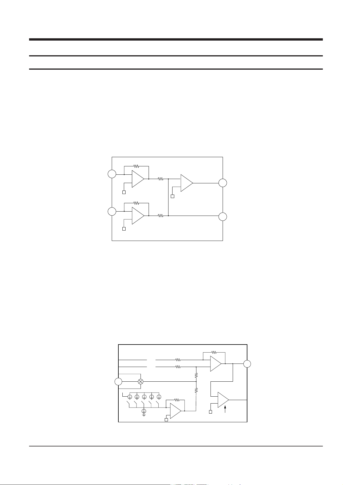
The two currents from input pins PD1 (A+C) and PD2 (B+D) are converted into voltages through I/V Amp,
and they are added to RF summing Amp. The photo diode (A+B+C+D) signal which is I-V changed is
outputted by RFO (pin74). At this pin, the eye pattern can be checked.
The output of the focus error amp is the difference between RF I-V AMP(1) output Va and RF I-V AMP(2)
output Vb,just is the Photo Diode ((A+C) - (B+D)) signal which is I-V changed.
The focus error bias voltage applied to the (+) of focus error amp can be changed by D/A converter as shown in
diagram, so that the offset of focus error amp can be adjust automatical.
Focus error bias can be adjusted from the range of +100mV ~ -100mV by connectiong the resistor with pin 63
(FEBIAS).

Special Circuit Descriptions
5-2 Samsung Electronics
5-1-3 Tracking Error Amp
5-1-4 Focus OK Circuit
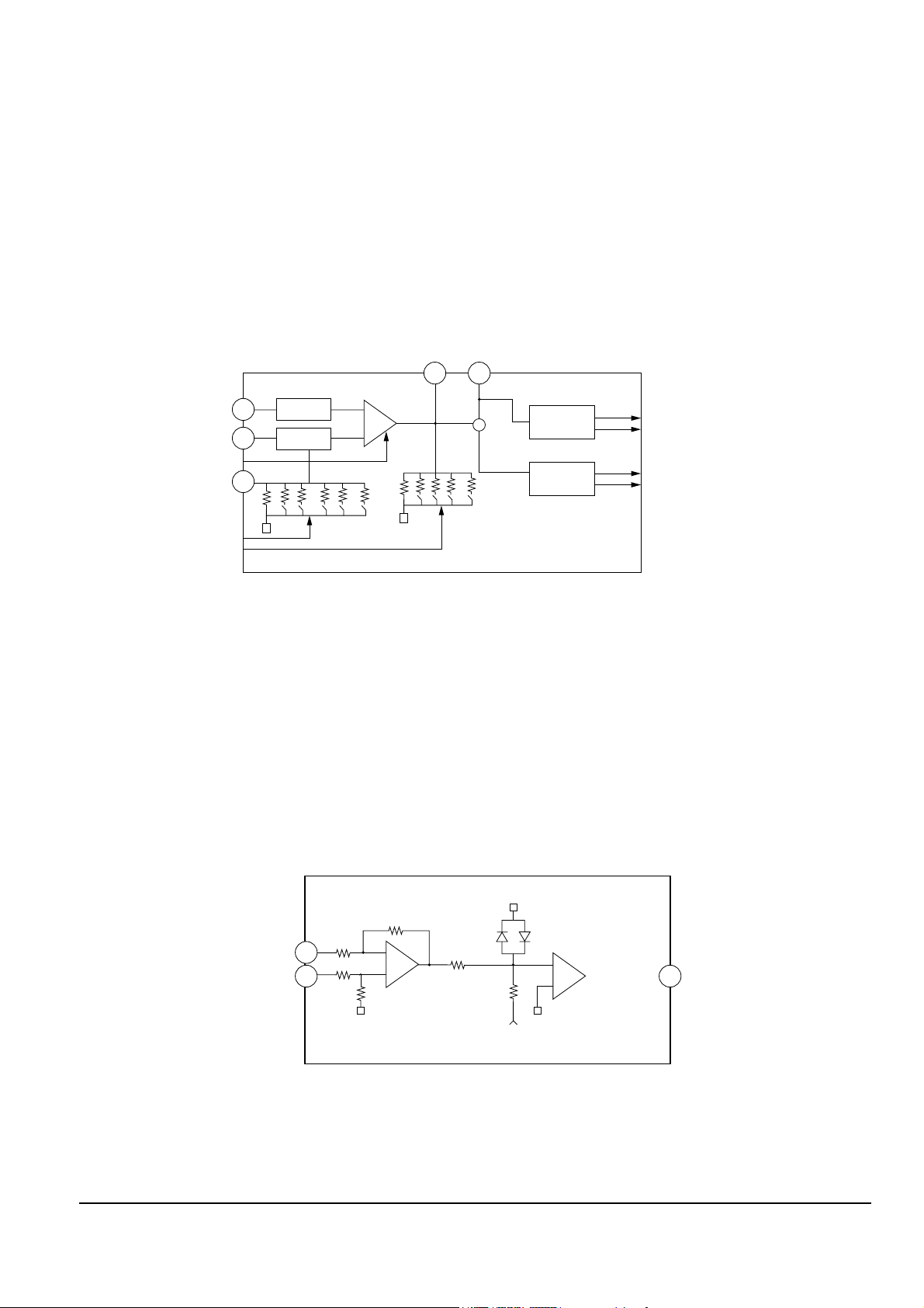
The current signals from the side spot photo diode (E and F) are input to the E and F pin and converted into
voltage signals by E I-V and F I-V AMP. The output of tracking error amp is due to the difference between
E I-V AMP voltage output.
The E-F balance can be adjusted by modifying the gain of E I-V AMP, and the tracking gain(Pin TE1) can be
adjusted automatically by micom program.
Extracting the DC part of RFI and RFO and comparing with the basic DC level, if RF Level is more than basic
level, the FOK is output. The focus OK circuit generates a timing window of focus on to monitor the focus
search status of focus serve.
+
-
79
68
67
F
E
EI
TGFI
BAL< 4 0 >
GAIN< 3 : 0 >
from Digital
TGL
TGH
TE1
LPFT
BALL
To ISTAT,TRCNT
BALH
GAIN-UP/DOWN
75K
220K
110K
56K
27K
13K
13K
16K
7.5K
3.3K
1.5K
IV AMP
IV AMP
WIN COMP
WIN COMP
54 55
-
40K
40K
40K
90K
57K
FOK
VC+0.625V
+
-
74
75 40
+
-

Special Circuit Descriptions
Samsung Electronics 5-3
5-1-5 Mirror Circuit
5-1-6 EFM Comparator
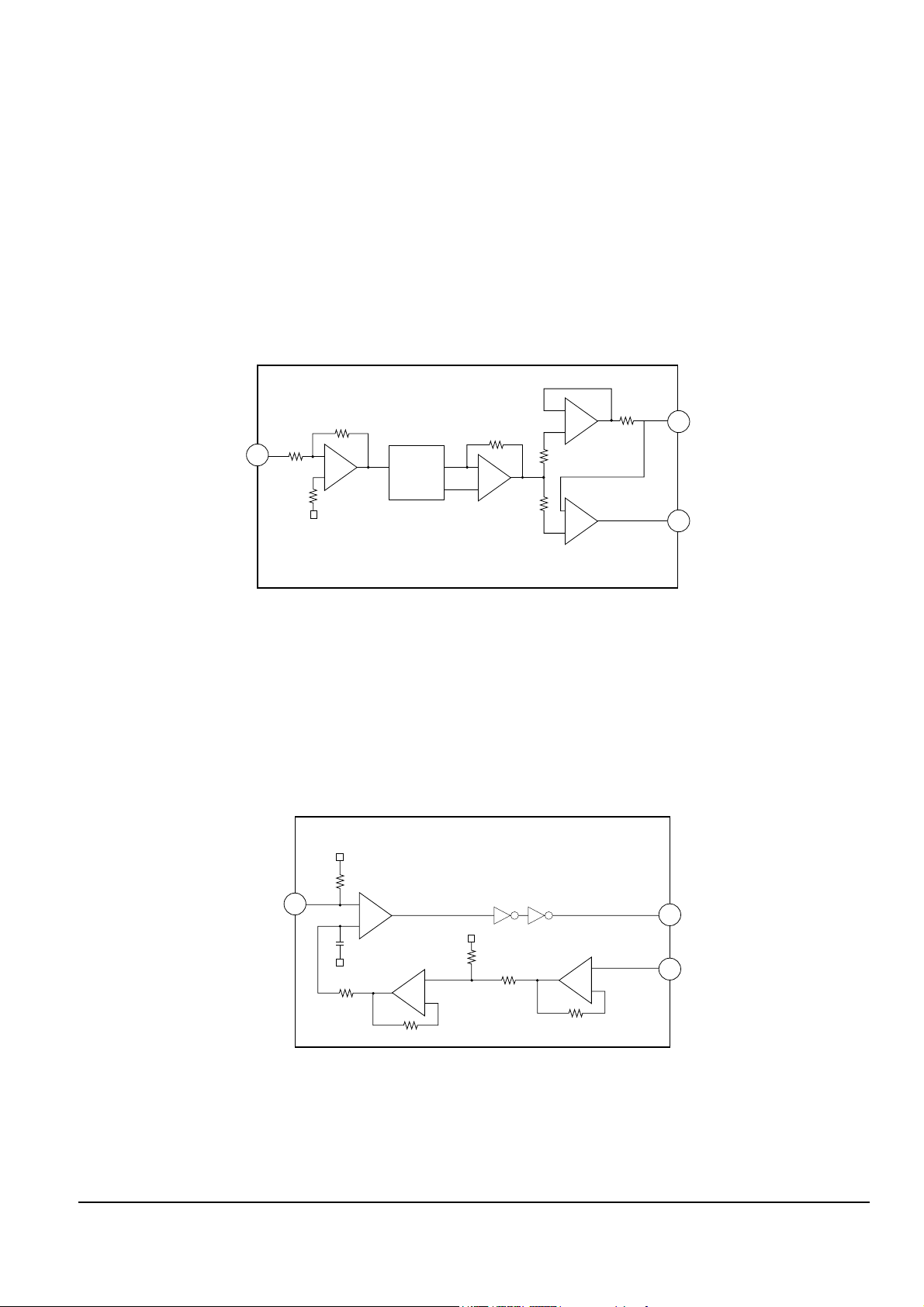
After RFI signal is amplified by mirror amp, mirror signal is held in peak and bottom circuit. The following of
100KHZ traverse is possible in peak hold circuit and the loss of track count due to defect is counted in bottom
hold circuit. Mirror output beyond 2KHz is. ÒLÓ at track on disc, ÒHÓ at interval between track on disc, ÒHÓ
when the defect beyond 1.4ms is detected.
The time constant for the mirror hold must be sufficiently large than of the traverse signal
The EFM comparator converts a RF signal into a binary signal
As the asymmertry due to variations in disc manufacturing can not be eilminated by thr AC coupling alone,
the reference voltage of EFM comparator is controlled utilizing the fact that the generation probability of 1,0
50% each in the binary EFM signals.
+
-
+
-
+
-
+
-
75
1
39
38K
96K
17K
1.5K
2.5K
17K
19K
IRF
MIRROR
MCP
Peak and
Bottom
Hold
+
-
+
-
+
-
77
1
39
40K
100K
100K
20K
85K
19K
RFI
EFM
ASY
 Loading...