

SAMSUNG MAX460V Service Manual
3CD CHANGER MINI COMPONENT
1. Precautions
2. Specifications
3. Disassembly and Reassembly
4. Alignment and Adjustments
5. Special Circuit Descriptions
6. Troubleshooting
7. Exploded Views and Parts List
8. Electrical Parts List
9. Block Diagrams
10. PCB Diagrams
11. Wiring Diagram
12. Schematic Diagrams
SERVICE
Manual
3 CD CHANGER VIDEO CD
MINI MINI COMPONENT
MAX-460V
CONTENTS
©
Samsung Electronics Co., Ltd. Dec. 1996. Code No. AH68-20139A

2. Specifications
Power source
Power consumption
Dimensions (mm)
220V 50Hz(Option)
150W
270(W) x 315(H) x 335(D)
Power output
Total harmonic distortion
Frequency range
Signal to noise ratio
Channel separation
Input sensitivity
Frequency range
Usable sensitivity
Signal to noise ratio
IF rejection ratio
Total harmonic distoration
Separation (Stereo)
Frequency range
Usable sensitivity
Signal to noise ratio
IF rejection ratio
Total harmonic distortion
Frequency range
Usable sensitivity
Signal to noise ratio
Frequecny range
WOW FLUTTER
Erasing effect
Signal to noise ratio
Total harmonic distortion
Frequency response
Signal to noise ratio
Channel separation
Total harmonic distortion
87.5 ~ 108MHz
8µV
55dB
60dB
0.7%
23dB
522 ~ 1611KHz
600µV
40dB
45dB
2%
146 ~ 290KHz
1250µV
35dB
125Hz ~ 8KHz
0.35%
55dB
45dB
2%
20Hz ~ 20KHz(¡ 1dB)
95dB(1kHz 0dB)
75dB(1kHz 0dB)
0.05%(1kHz 0dB)
40W/CH(6Ω)
0.5%
20Hz ~ 20kHz
75dB
50dB
400mV
General
Amplifier
Tuner
Cassette
Compact Disc
FM
LW
MW
(AM)
Samsung Electronics 2-1
* Specifications are subject to change without notice.
(OPTION)
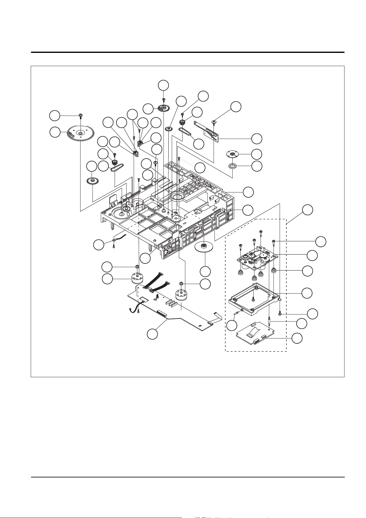
3. Disassembly and Reassembly
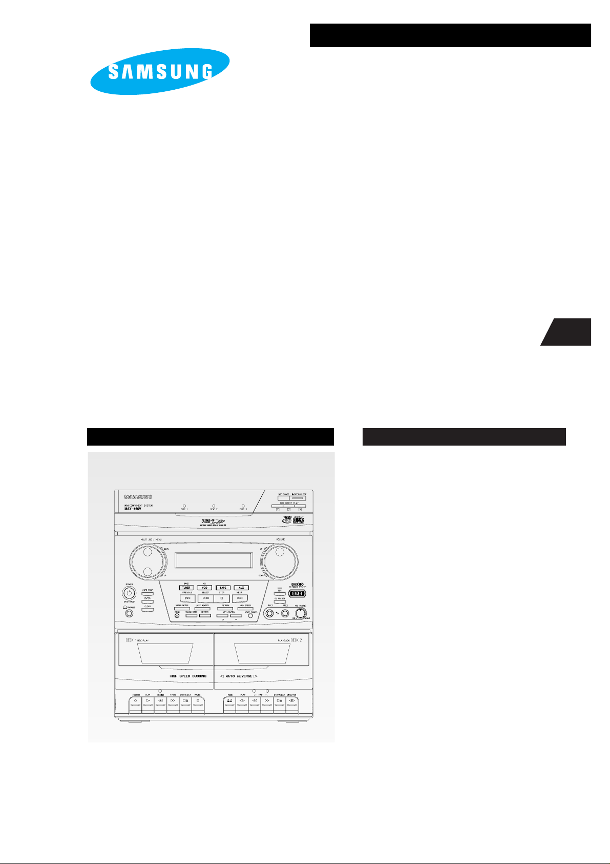
3-1 Cabinet-Top
1. Remove 11 screws holding the cabinet-top.
2. Lift the back of the cabinet-top and slide it to the rear to remove. (See arrow)
Samsung Electronics
3-1
Figure 3-1
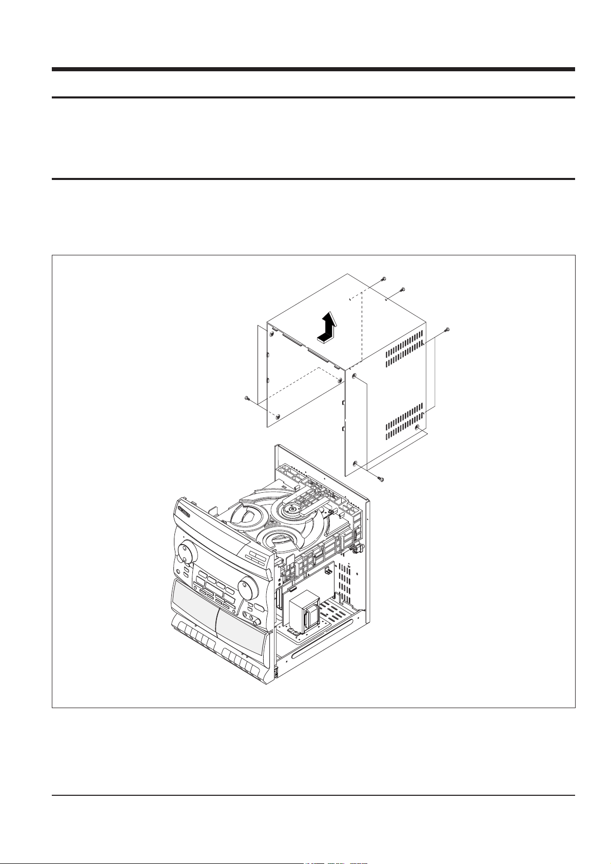
3-2 CD-MECHA, DOOR-CD
1. If power is connected :
- Turn power on
- Open the tray using the open/close key
- Remove the Door in the direction of arrow #.
2. If power is not connected :
- Turn the gear clockwise using a screw driver as shown in Figure 3-2- 1.
- Pull the Tray in the direction of arrow @ and then remove the Door in the direction of arrow # .
3. Remove 2 screws $ and lift the CD-MECHA.
1
2
3
4 4
4 4
3-2
Samsung Electronics
Figure 3-2-1
Figure 3-2
Disassembly and Reassembly
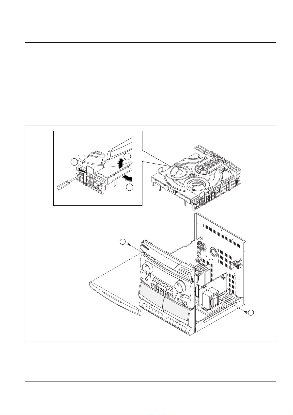
3-3 Cabinet-Rear and Main PCB
3-4 Cabinet-Front and Cabinet-Bottom
1. Remove 14 screws % and then lift the cabinet-rear ^ and slide it to rear to remove (see arrow).
2. Remove the Main-PCB & to rear.
A A
BB
8 8
8 8
1. Remove 5 screws *.
2. Remove the cabinet-rear by pushing the "A" and "B" as shown.
Samsung Electronics 3-3
Figure 3-3
Figure 3-4
7 7
66
55
55
Disassembly and Reassembly
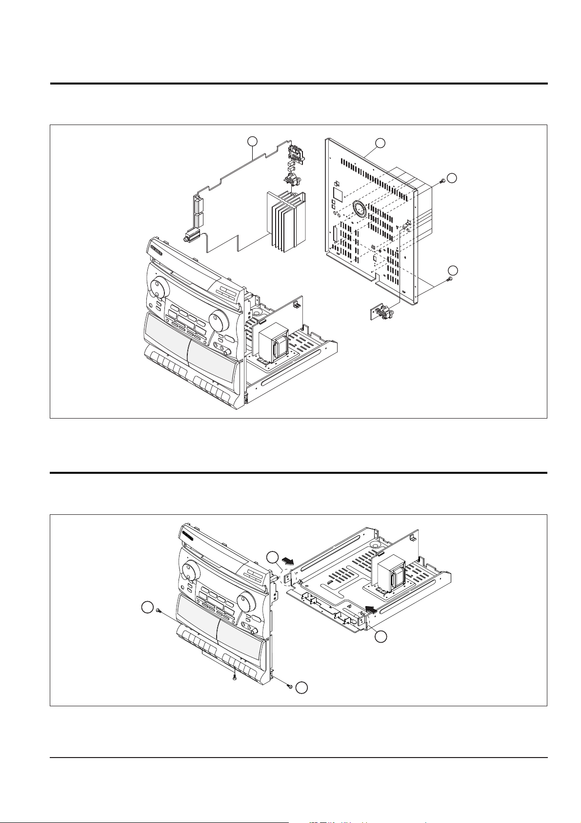
3-5 CD Mecha Main
3-4 Samsung Electronics
Figure 3-5
11
34
30
36
17
33
5
4
9
28
7
8
6
32
10
18
26
25
29
16
16
1
3
22
2
24
21
20
19
35
31
13
15
14
4
6
5
7
1
3
2
8
37
27
12
Disassembly and Reassembly

3-5 CD Mecha Main Continued
3-6 CD-PCB
1. Turn the Bracket-chuck ! counter clockwise to remove.
2. Remove the Table-Chuck union @.
3. Remove the Magnet-Chuck #.
4. Remove the screw $ and then lift the Gear-Tray(2) %.
5. Remove the Belt-disc ^.
6. Remove the screw & and then lift the Gear-Pulley * .
7. Lift the Gear-Tray(1) ( .
8. Remove 2 screws and then remove the Motor-DC 1.
9. Remove the Pulley-Motor 2.
10. Remove 1 screw Y and then remove the PCB-SUB switch 3.
11. Remove the Switch-Micro 4 with using the soldering iron.
12. Remove the Connector-Wafer 5with using the soldering iron.
13. Remove 2 screws 6 and then remove the Gear-Cam 7.
14. Remove the Belt-Disc 8.
15. Remove 1 screw Y and then remove the PCB-SUB switch 9.
16. Remove the Switch-Micro 0 and the Connector-Header “.
17. Remove the Pulley-Motor =.
18. Remove 1 screw Q and then lift the Gear-Pulley q.
19. Remove 1 screw W and then lift the Gear-UD(2) w.
20. Lift the Gear-UD (1) E.
21. Remove 1 screw and then remove the Clamp-Wire D.
1. Remove 2 screws !.
2. Remove the PCB @ with using the soldering iron.
3. Remove the Hook #.
4. Remove four Shaft-CD$ and then remove four Rubber-CD %.
5. Remove the CD-Deck ^ and Lever-Lift & is removed automatically.
6. Remove the Shaft *.
Samsung Electronics 3-5
* Refer to U of Figure 3-5.
Disassembly and Reassembly
3-7 CD Mecha Tray
1. Remove 1 screw ! and then remove the Roulette @ .
2. Remove 6 Cushions + .
3. Remove 2 Washers # .
4. Remove the Gear-Roulette(2) $ and then remove the Gear-Roulette (1) %.
5. Remove 3 screws ^ and then remove three Cushion-Bracket & .
6. Remove 3 Cushion-Motors * .
7. Remove 2 screws ( and then remove the Motor-DC 1 .
8. Remove the Bracket-Motor ) .
9. Remove the Shaft-Motors(1) 1 .
10. Remove the Gear-Worm 2 from the Motor-DC.
11. Remove the PCB-SUB Motor(R) 3 with using the soldering iron.
12. Remove the A/S, C/wire 4 with a soldering iron.
13. Remove 1 screw 5 and then remove the connector-header 6, Sensor-Roulette 7 and the A/S, C/wire(FL)
8 with using a soldering iron.
14. Remove the PCB-SUB sensor(R) 9.
20
4
16
3
23
2
10
22
11
19
13
17
8
14
5
21
1
7
6
12
9
22
18
15
3-6
Samsung Electronics
Figure 3-6
Disassembly and Reassembly
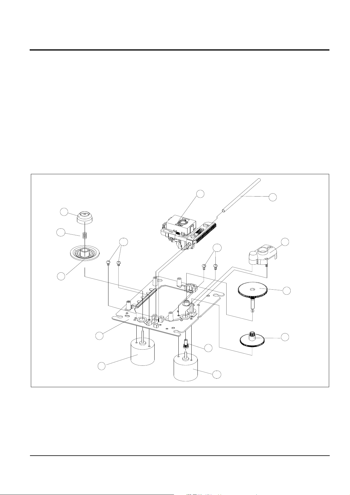
3-8 CD Deck
1. Remove the Shaft ! .
2. Lift the P/U @ .
Note : Take extreme care not to touch the surface of lens.
3. Lift the Center-ring # .
4. Remove the Spring-T/Table $ .
5. Remove the Turn-Table (M) % .
6. Remove 2 screw ^ and then remove the Spindle-Motor & .
7. Remove the Cover-Gear * by pushing the hook.
8. Remove the Gear(c) ( by pushing the hook.
9. Lift the Gear(b) ) .
10. Remove the Gear(a) 1 .
11. Remove 2 screws 2 and then remove the Feed-Motor 3 .
12. Remove the Chassis-Deck(M) 4.
3
4
5
6
12
2
1
8
9
10
11
13
14
7
Samsung Electronics 3-7
Figure 3-7
Disassembly and Reassembly
4. Alignment and Adjustments
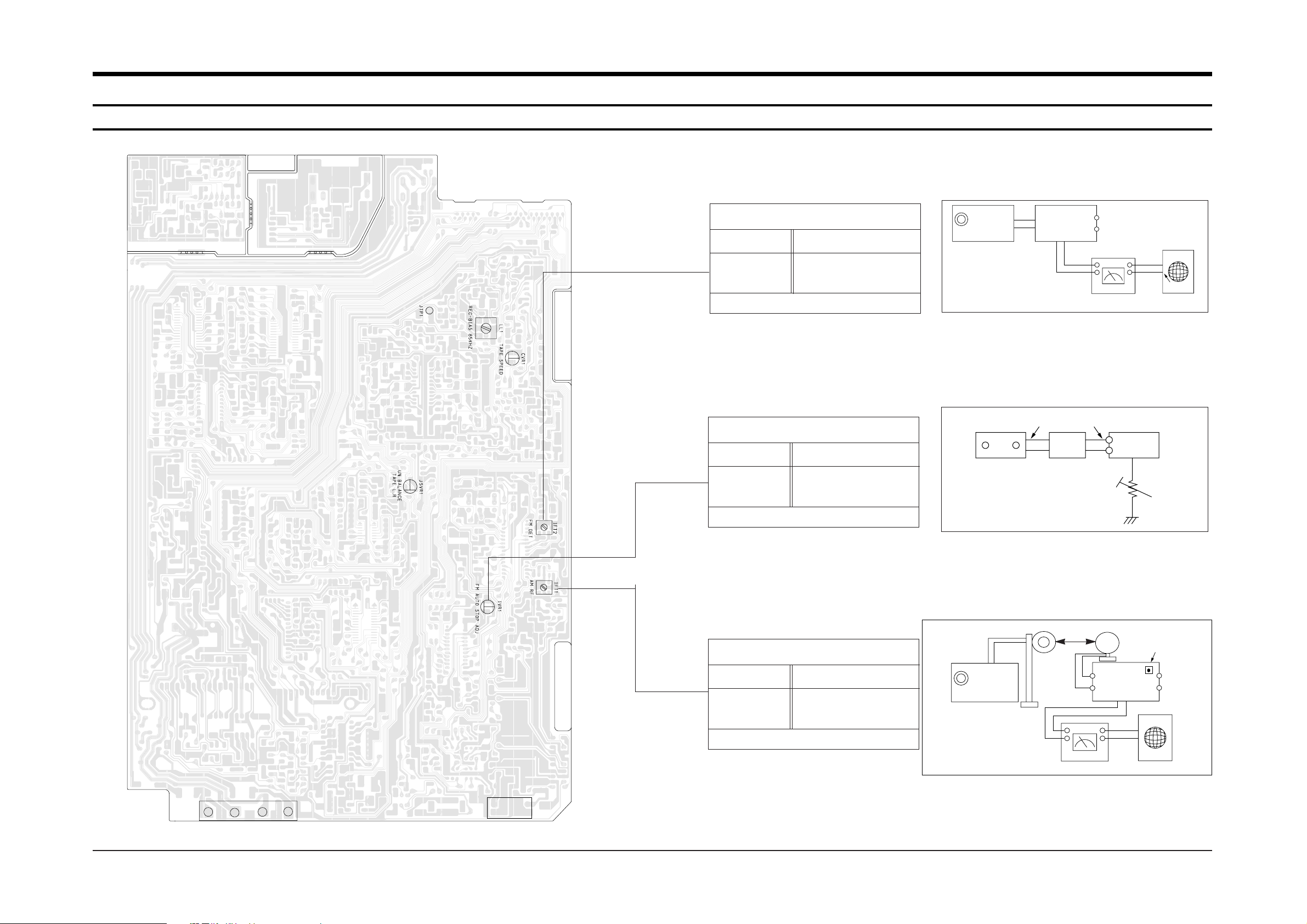
4-1 Tuner
FM T.H.D Adjustment
SSG FREQ. 98MHz
Adjustment
point FM DETECTOR COIL
(IFT2)
Minumum Distortion(Figure 4-1)
FM Search Level Adjustment
SSG FREQ. 98MHz
Adjustment
point SEMI-VR(5KB)
(IVR1)
"TUNED" is shown on FLT(Figure 4-2)
FM
Antenna
Terminal
Speaker
Terminal
Input
Input
Figure 4-1 IF CENTER and T.H.D Adjustment
Figure 4-2 FM Auto Search Level Adjustment
Output
Distortion Meter
Oscilloscope
Oscilloscope
FM SSG
FM SSG
GND
26dB
75Ω
Dummy
FM IN
FM Antenna
SET
5 kB
SET
Output
GND
AM(MW) I.F Adjustment
SSG FREQ. 450KHz
Adjustment
point AM I.F COIL
(IFT1)
Maximum output(Figure 4-3)
Figure 4-3 AM I.F Adjustment
AM ANT
60cm
IFT1
IN
AM SSG
450KHZ
Speaker Terminal
INPUT
OUTPUT
OUTPUT
VTVM
4-1Samsung Electronics
SPEAKER JACK
L
R
FM
AM
ANT JACK
Figure 4-4
Figure 4-6
4-2 Cassette Deck
4-2-1 Test Equipment
1. Oscilloscope
2. VTVM
4-2-1(a) TAPE
1. MTT-111 (or equivalent) : Test tape on which 3KHz signal is recorded (Tape speed adjustmant)
2. MTT-5512 (or equivalent)
3. MTT-113CN (or equivalent) : Test tape on which 8KHz signal is recorded (Azimuth)
4. MTT-112B (or equivalent) : Test tape on which 1KHz signal is recorded (L.R. channel unbalance)
AZIMUTH Adjustment
Screw
REC PB Head
INSET
Frequency
Counter
Speaker
Terminal
SET
(GND)
VTVM
V H
Figure 4-5
Oscilloscope
IN
OUT
OUTPUT
Item
Connection
Preparation
Tape speed
(normal speed)
adjustment
Figure 4-4
Figure 4-4
3 KHz
5200Hz ~ 6600Hz
CVR1
JPT1
Tape speed
(high speed)
1) Insert MTT-111 to
Deck 2.
2)Press PLAY button.
1) Insert MTT-111 to
Deck 2.
2) Insert MTT-5512
to Deck1.
3) Press Hi-SPEED
button.
4) Press RECORD
button.
Remark
Adjustment Point
Samsung Electronics4-2
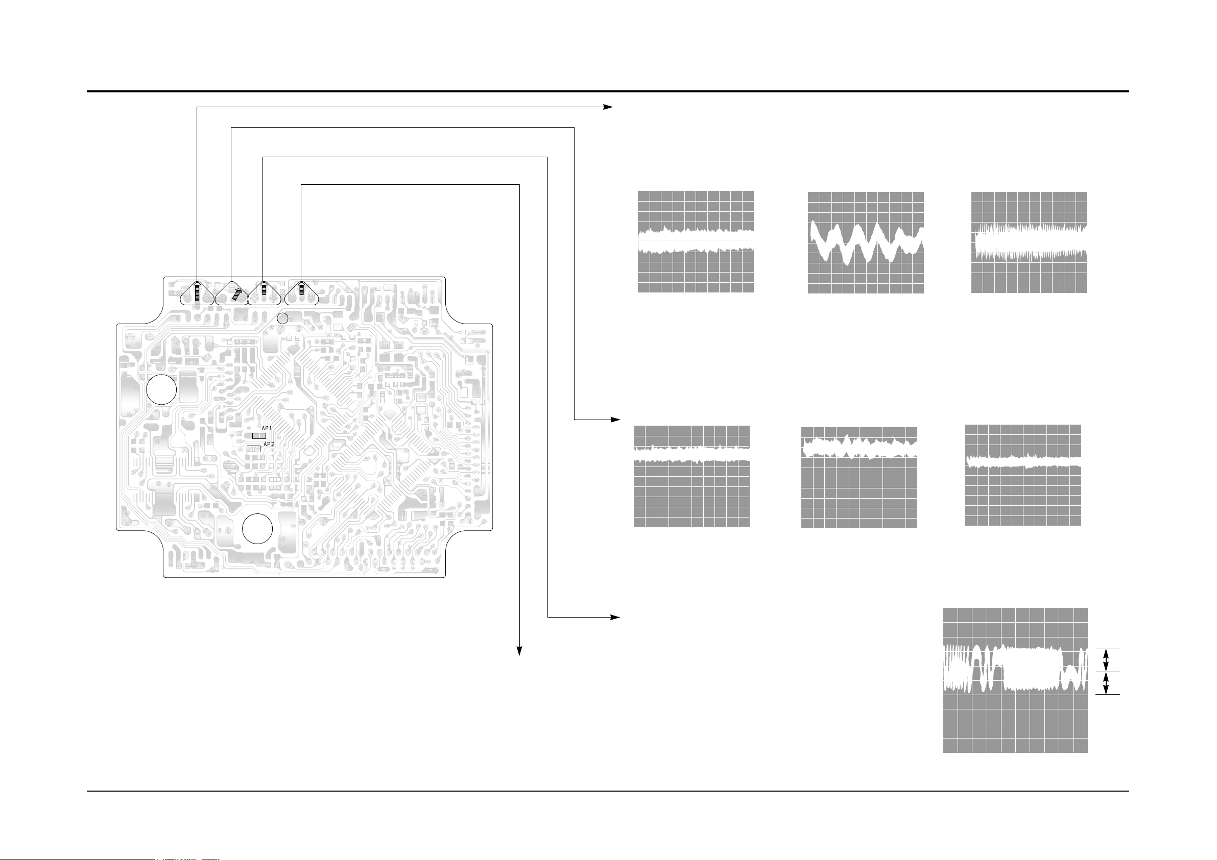
4-2-2 Location of Adjustment Points (Refer to page 4-1)
4-2-3 Adjustment Procedure
4-2-3(a) TAPE SPEED
4-2-3(b) AZIMUTH
1. DECK 1
2. DECK 2
Maximum output and
identical phase of L,R
channel.
Set the screw after
adjustment.
Maximum output and
identical phase of L,R
channel.
Set the screw after
adjustment.
Item
Connection
Preparation
AZIMUTH
Figure 4-5
L-CH R-CH
0.5dB
Figure 4-6
JSVR15L
L,R unbalance
Play MTT113N
in the DECK1.
Play MTT112B
in the DECK1.
Remark
Adjustment Point
Item
Connection
Preparation
AZIMUTH
Figure 4-5
Figure 4-6
Play MTT113N
in the DECK2.
Remark
Adjustment Point
3. Recording Frequency
85KHz
Item
Connection
Preparation
Bias oscillation
frequency
LL1
Record
MTT5512
in the DECK1.
Remark
Adjustment Point
Alignment and Adjustments
4-3Samsung Electronics
4-3 CD
WVR1
T.G
WVR2
F.G
WVR3
E/F. B
WVR4
F.B
Vref
0V
A
B
A=B
---100mV
---0V
---250mV
---0 V
---100mV
---0 V
---0 V
---0 V
---0 V
4-3-1 To Adjust FOCUS BIAS(STOP mode)
4-3-3 To Adjust Focus Gain (PLAY mode)
4-3-2 To Adjust Tracking Gain (PLAY mode)
4-3-4 To Adjust E/F Balance (PLAY mode)
1. Set Volt/Div of the oscilloscope to DC 100mV.
2. Ground the scope input and set the waveform to 0V, DC range.
3. Connect the GND terminal of the oscilloscope to
Vref, and (+) terminal to center of AP1.
4. Set WVR4 to 0mV.
1. Connect the GND terminal of the oscilloscope to Vref and (+) terminal to AP2.
2. Load and play the disc
3. While the disc is running adjust the gain with WVR1 as shown below.
1. Connect the GND terminal of the oscilloscope to Vref and (+) terminal to AP1.
2. Load and play the disc
3. While the disc is running adjust the gain with WVR2 as shown in the following figure.
VOLT/DIV : 0.2V
TIME/DIV : 2mS
Normal frequency
Normal frequency
Low frequency
High frequency
Low frequency
High frequency
VOLT/DIV : 0.1V
TIME/DIV : 2mS
VOLT/DIV : 0.1V
TIME/DIV : 2mS
VOLT/DIV : 0.1V
TIME/DIV : 2mS
VOLT/DIV : 0.2V
TIME/DIV : 2mS
VOLT/DIV : 0.2V
TIME/DIV : 2mS
1. Set TIME/DIV of the oscilloscope to 2mS.
2. Set Volt/DIV of the oscilloscope to 0.5V.
3. Ground the scope input and set to DC
and then set the DC range.
4. Connect the GND terminal of the oscilloscope to Vref
and (+) terminal to center to AP2.
5. Load and play the disc.
6. Turn WVR1 counterclockwise to the minimum value.
7. Raise WVR3 and adjust the waveform so that its middle
comes to GND of the oscilloscope (or until the upper half
of waveform becomes symmetrical to the bottom half, A=B)
8. Adjust WVR1 (arrow) for normal sound.
Alignment and Adjustments
RF I-V Amp(1) and RF I-V Amp(2) currents are converted to voltage via
internal resistance of 58k½ from the current of PD1(A+C) and PD2(B+D):
These voltage are added by the RF summing amplifier.
The signal (A+B+C+D) is applied to RFO (No. 2 terminal).
RF output voltage is calculated as follows :
VFE = (R2/R1) x (V2-V1) = 5.4(V2-V1)
This FOCUS ERROR voltage is sent to FOCUS SERVO .
VRF = -R3 x (iPD1 + iPD2)
VRF = -R3 x (V1/R1 + V2/R2)
VRF = -R3 x ( + )
VRF = - x (V1 + V2)
10K 10K
V 1 V 2
10K
R3
74
Photo Detector
B
CA
D
PD1
PD2
58K
RF I-V AMP(1)
58K
10K
R2
RF I-V AMP(2)
V2
R1
10K
RF SUMMING
V1 AMP
RFO
RF
66
67
R3
75
5-1-1 RF Amp (KA9220) : NIC9220
5-1-2 FOCUS ERROR Amp(KA9220) : NIC9220
57
63
R2
174K
C1 25P
FE
FOCUS
ERROR
AMP
164K
FE Bias
GNDVcc
20K
32K
C2 25P
-(A+C)
-(B+D)
R1
V1 32K
5-1-3 FOCUS SERVO SYSTEM (KA9220) : NIC9220
When FS3 is ON, high frequency gain decreases (time constant set by pin17, pin19 ; capacitor is connected
to internal resistance).
The capacitor between pin 18 and GND sets the time constant to pass the low frequencies in PLAY mode.
The maximum frequency of the focus phase compensation is inversely proportional to the resistance connected to
pin 7. Focus search peak is about 1.1 Vp-p, and is inversely proportional to the resistance connected to pins 22,23
(if this resistance changes, the peak of track jump and sled kick change).
The inverted input of FZC comparator is set to 5.7% of the difference between Vcc and VC(pin69) {{5.7% x (Vcc-Vc)}.
Note : If the resistance connected to pin7 changes, the phase compensation peak of the focus tracking sled
servos change. (The 'op-amp' dynamic range and offset voltage also change.)
3.6K
20
21
47
48
60K
FZC
0.0022
20K
0.1UF
0.1UF
FDFCT
HFGD
EFR
FE2
470K
DFCT
FS4
20K 48K
58
60
62
46K
580K FS3
FSW
470K
130K
0.1UF
27
40K
6
PFSET
FS2
PHASE
COMPENSATION
92K
40K
10K
3
4.7UF
FSCH
FS1
50K
5.5U 11U
VREG
180K
ISET
FCE
120K
FOCUS
COIL
FSEO
FE1
61
Samsung Electronics
5-1
5-1 CD
FOCUS ERROR Amp amplifies the difference
between RF I-V Amp(1) output (A+C) and RF I-V Amp(2)
output(B+D).
These two signals are supplied to (-) and (+) input terminals of
FOCUS ERROR Amp. The FOCUS ERROR output is applied to
FE (Terminal No.57).
The FE output voltage of this low frequency component varies
according to {(A+C) - (B+D)}.
VFE is calculated as follows :
5. Special Circuit Descriptions
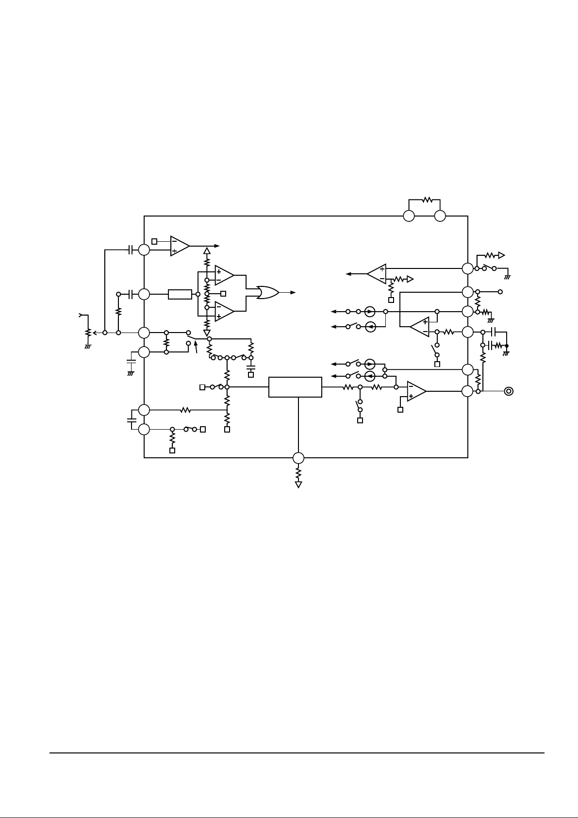
5-1-4 TRACKING SLED SERVO SYSTEM (KA9220) : NIC9220
The capacitor between pin 15 and 16 attenuates high frequencies when TG2 is off. The maximum frequency of
tracking phase compensation is inversely proportional to the resistance connected to pin 7 (about 1.2kHz at 470k).
The tracking jump (FWD and REV) is determined when TM3 and TM4 are ON, and the peak voltage induced from
the tracking coil is determined by both TM3 and TM4 currents and the feed back resistance of pin 47.
Track jump max voltage = TM3 (TM4) current x feedback resistance.
FWD or REV sled kick occurs when TM5 or TM6 is ON, and the peak voltage added to sled motor
(determined by TM5 or TM6 current and the feedback resistance of pin 41.)
Sled jump max. voltage = TM5(TM6) current x feedback resistance
Each SW current is determined by the resistance connected to pin 22 and 23.
When the resistance is about 150½,
TM3 or TM4 = 11µA,
TM5 or TM6 = 22µA,
This current is inversely proportional to the resistor, variable within a range of t 5 to 40 µA for TM3.
STOP is the ON/OFF detection signal for the limit SW (or the sled motor's innermost cirumference).
22 23
40
41
39
47
48
7
15
16
54
52
50
51
0.022UF
TZC
0.047UF
150K
BPF
1K
1K
TZC
100K
ATC
20K
TE 1
TE2
470K
100K
ATS
TDFC1
0.1UF
680K
66PF
10K
DFCT
0.1UF
RTG
20K
TGSW
470K
TG2
82K
110K
PHASE
COMPENSATION
S STOP
1K
100K
S STOP
SLED
SLEI
SLEN
10K
56K
100K
ISET VREG
180K
SLED
DRIVER
120K
100K
TKEO
TKEI
TM2
TM6
TM5
TM4
5.5U
TM3
5.5U
10K
90K
TM7
PFSET
470K
8
TRACKING
COIL
5-2 Samsung Electronics
Special Circuit Descriptions
Samsung Electronics 6-1
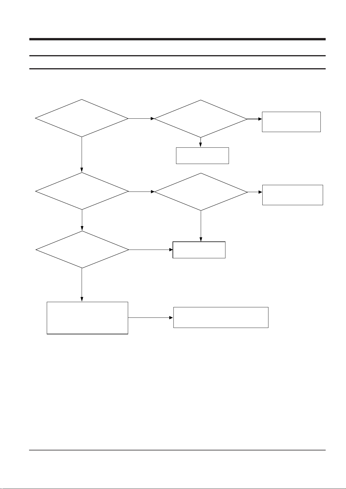
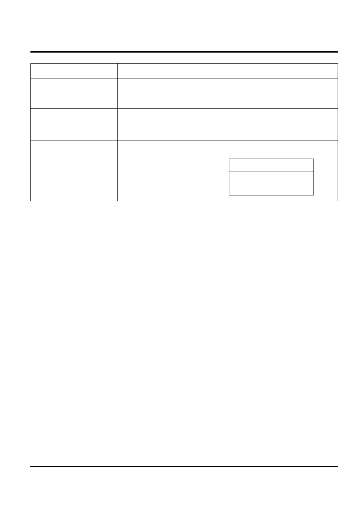
6. Troubleshooting
6-1 Amplifier
6-1-1 Power Malfunction
Front PCB µ-com VDD(5V)
normal?
UIC1 pin no. 18,47,90
Replace RIC1
Main PCB RIC1(BA3950) IN: 23V
Input voltage normal?
Yes
Check the Power PCB;
RD7,8,13(1N5392)
Yes
Front PCB
Does UX1(12MHz)
oscillate ?
FRONT PCB PWR-SENS
voltage normal ?
(pin no. 27 ; 5V)
Check the Main PCB
RD16,RR10,11,12,RC12
RD9
Yes
Front PCB
When the power is
ON 'H' displays
at pin no. 5 ?(5V)
Yes
Connect Front PCB and Main PCB.
Check the connector Main PCB.
Wafer MCW2
No
Replace µ-com.
Yes
No
No
No
No
Check the Power PCB : P/T, FUSE
No
6-2 Samsung Electronics
Yes
AQ103L,R Base B+ ?
Is Mute selected ?
Headphone Jack short ?
Remove it with Remocon.
Replace Headphone jack
soldering condition.
Main PCB AIC101
(STK4121,4141,4181-Option)
pin no. 9,11,12,14
B+,B- circuits
Check the B+ power
source part in RD1(PBL403),
RC2,3 and RIC1.
Yes
Confirm for TR short
replace it.
Check if the output line is
short.
No
No
No
No
Yes
Yes
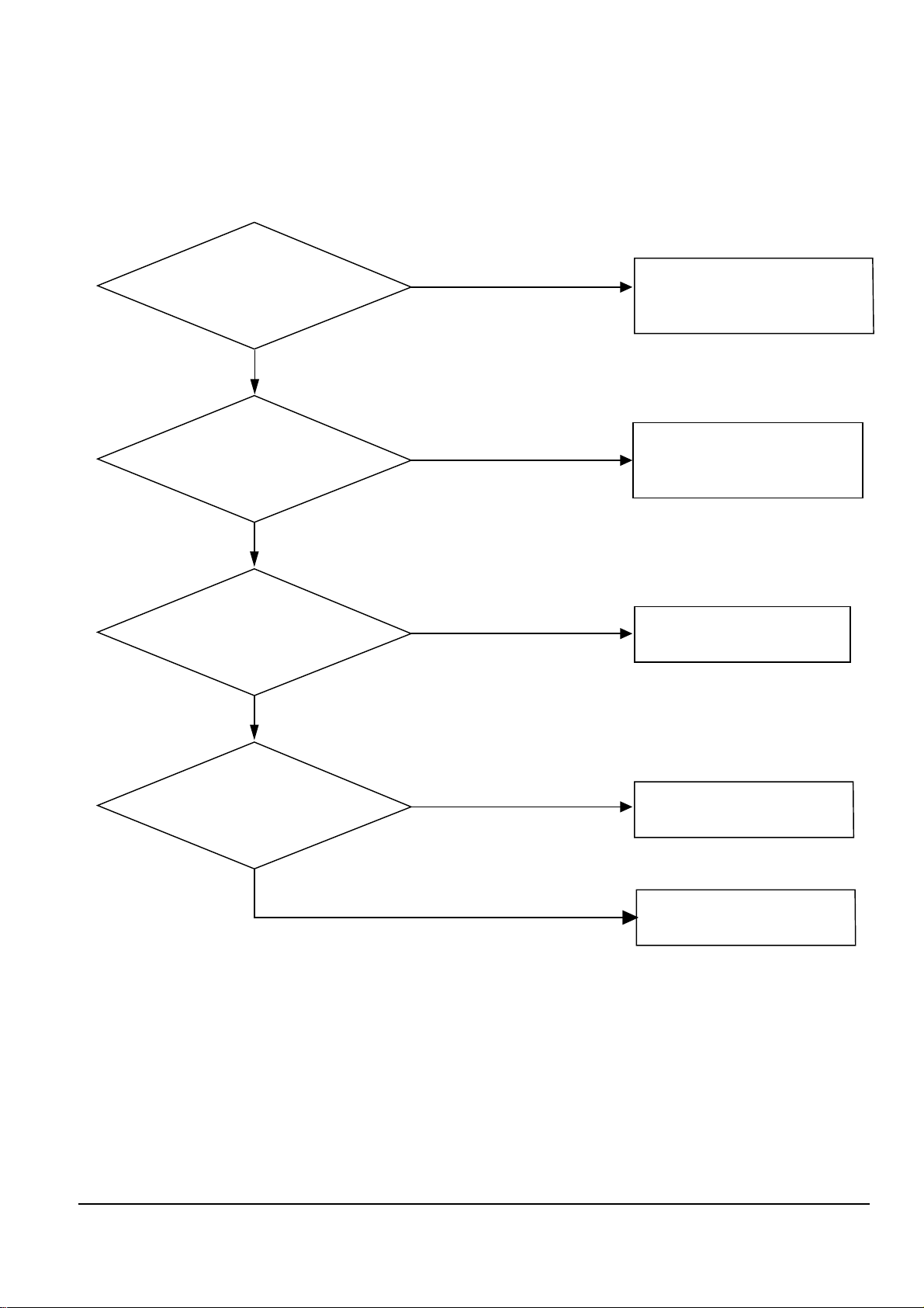
Troubleshooting
6-1-2 No Output
Samsung Electronics 6-3
IZD1(8.2V) Voltage ok ?
Yes
Check TUNER IC(LA1836)
pin no.10 ; 8.2V
pin no.14 ; 7.2V
AM ; 0V ?
Yes
LC72131
CONTROL ok?
Yes
FM VT
LC72131 pin no.20
1.7V 7.5V ?
Yes
AM VT
LC72131 pin 20
Check the LC72131
CONTROL ok?
Yes
Yes
Check HIC1
pin 20 ?
LPF1,2
output ok?
Check TDA7318 function ok?
Check FEP interior
pattern, and any line
disconnections.
1) Power impaired
so repair defects.
2) LC72131 Oscillator
(HX1 : 7.2MHz) ok ?
3) System line ok?
No
Yes
Check for µ-com IC
Replace LC72131
No
HZD1 (5.6V) Voltage ok?
HIC1 (LC72131) FM/AM BAND
Switching ok?
No
No
No
No
No
No
No
0.9V 7V
?
Power section defective
RIC1(BA3950) Voltage ok?
PIN NO.8 : 12V
Check the voltage ok ?
No
No
Troubleshooting
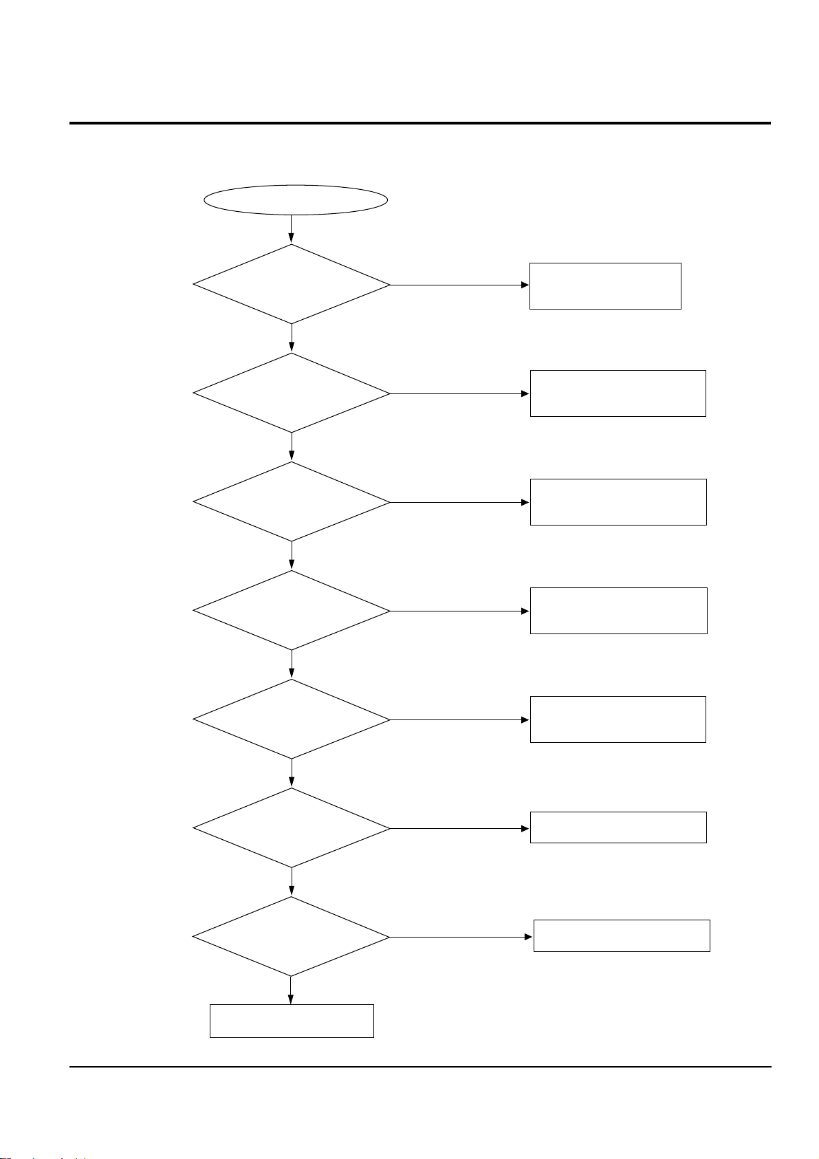
6-1-3 Tuner Malfunction (FM/AM)
6-4 Samsung Electronics
Yes
Connector inserted
correctly?
No
Yes
Check voltage : AC 4.8V
at FRONT-PCB FLT?
No
Check Main-PCB Front PCB
connection and the voltage of
MCW2, pins1,2(AC4.8V)
Yes
Check voltage at UIC1
pin no. 48(-30V)
No
Check the voltage of RD3(-30V)
Reinsert the connector.
Replace UIC1
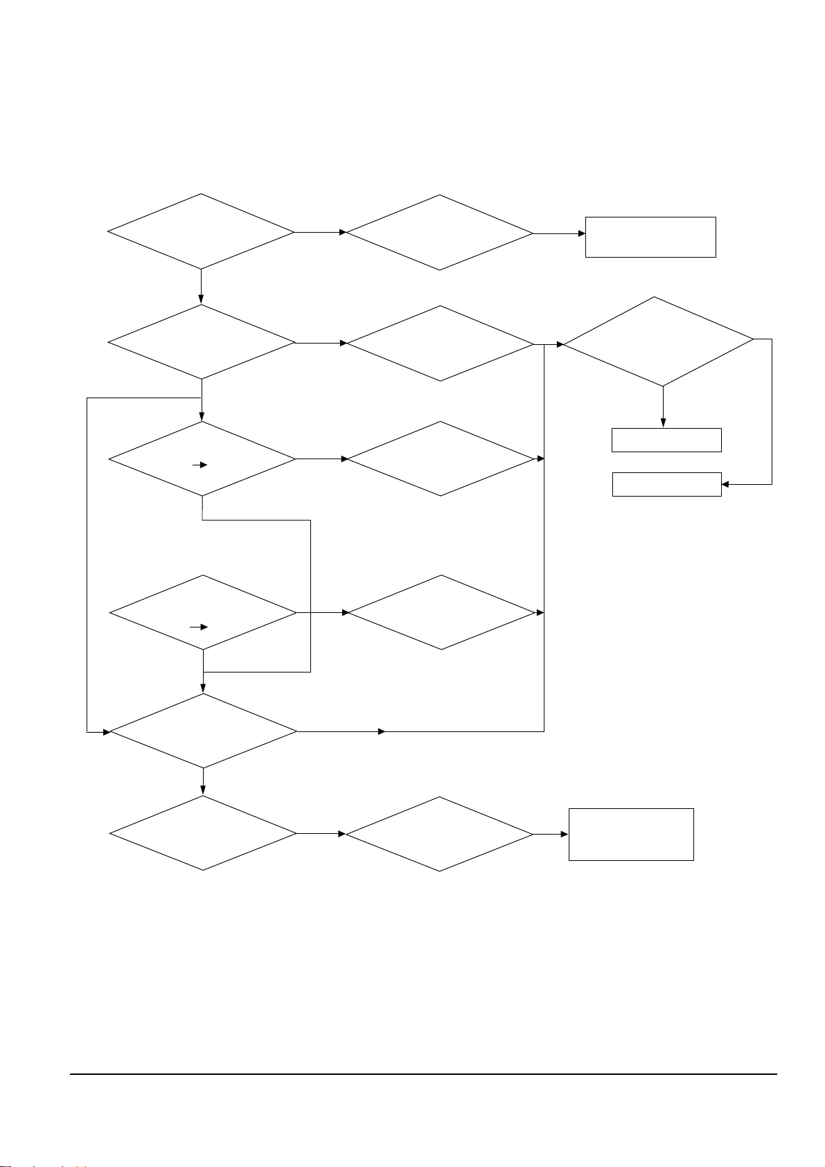
6-1-4 V.F.D Malfunction
Troubleshooting
Samsung Electronics 6-5
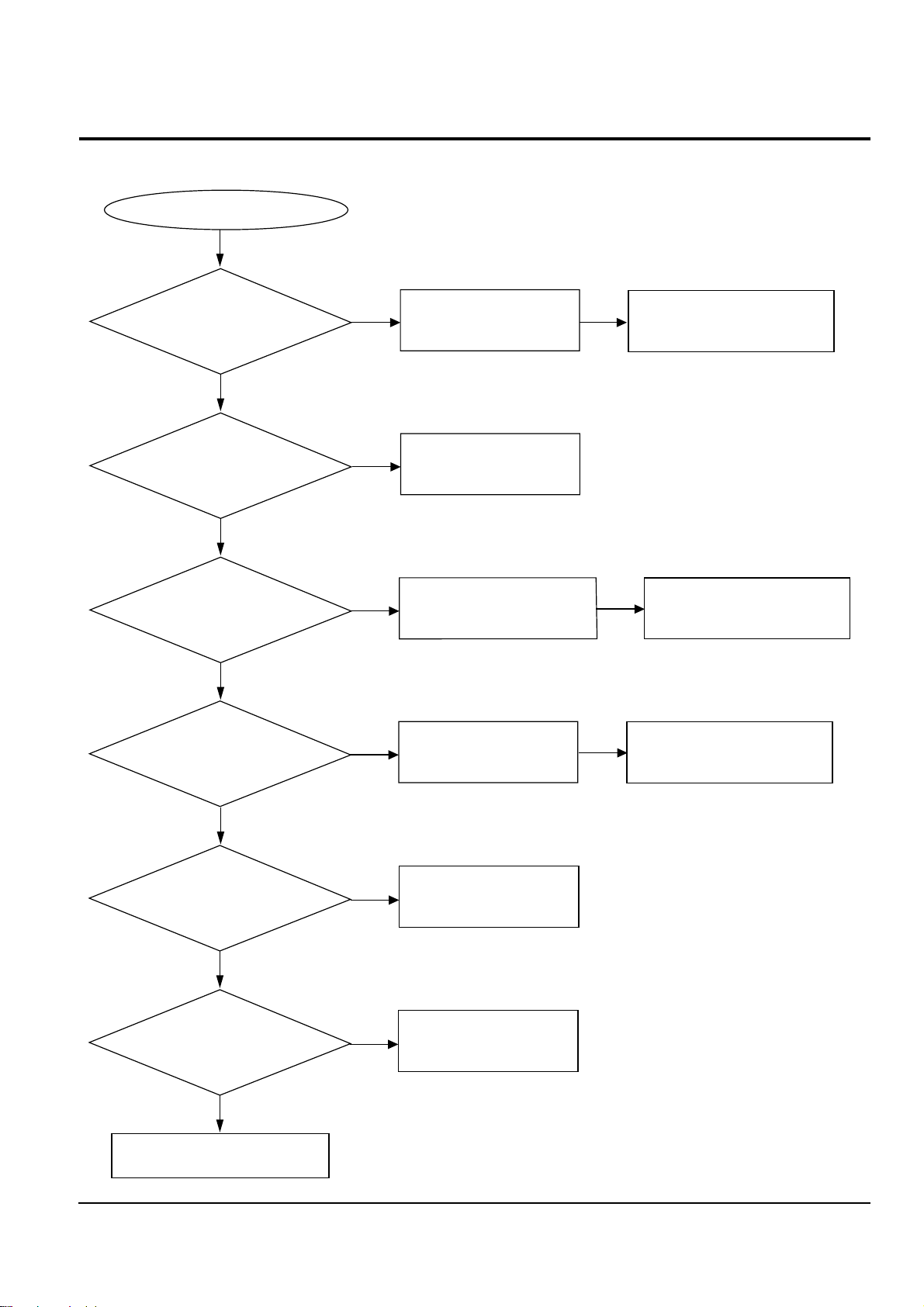
6-2 Cassette Deck
Troubleshooting
Block Main Function Check Point
TAPE IC JIC1
(KA22291)
Convert of P/B & R/P Signal
Check for voltage at pin5
1 P/B Deck : H
2 R/P Deck : L
Check for voltage at LC2
Osc Frequency : 85kHz
When inoperative : LQ4, LQ3 check
Convert of PLAY/RECORD
R/P Switching
Oscillate RECORD BIAS (85KHZ)
Check for voltage at pin no.16,8
BIAS OSC
Mode
Rec.
PLAY
9V
0V
Pin no.16,8
6-6 Samsung Electronics
Check UP/DOWN MOTOR
POWER ON
Check Deck down
Check CLOSE S/W voltage
Does Roulette revolve?
Check CLOSE MOTOR
and CLOSE S/W
Yes
No
Yes
Yes
Yes
No
No
Check Roulette Motor
Is Roulette Control ok?
Check Roulette Control Sensor
No
No
Yes
Yes
Is Focus Search ok?
Check oscillation of XX1
Yes
Yes
No
No
Does Laser function during
Focus Search?
Check WIC02 pin3 voltage
during Focus Search
:5V
Replace PICK UP
Replace CXD2500Q
Replace WIC01 or WIC03
(16.9344MHz)
CLOSE condition : 0V
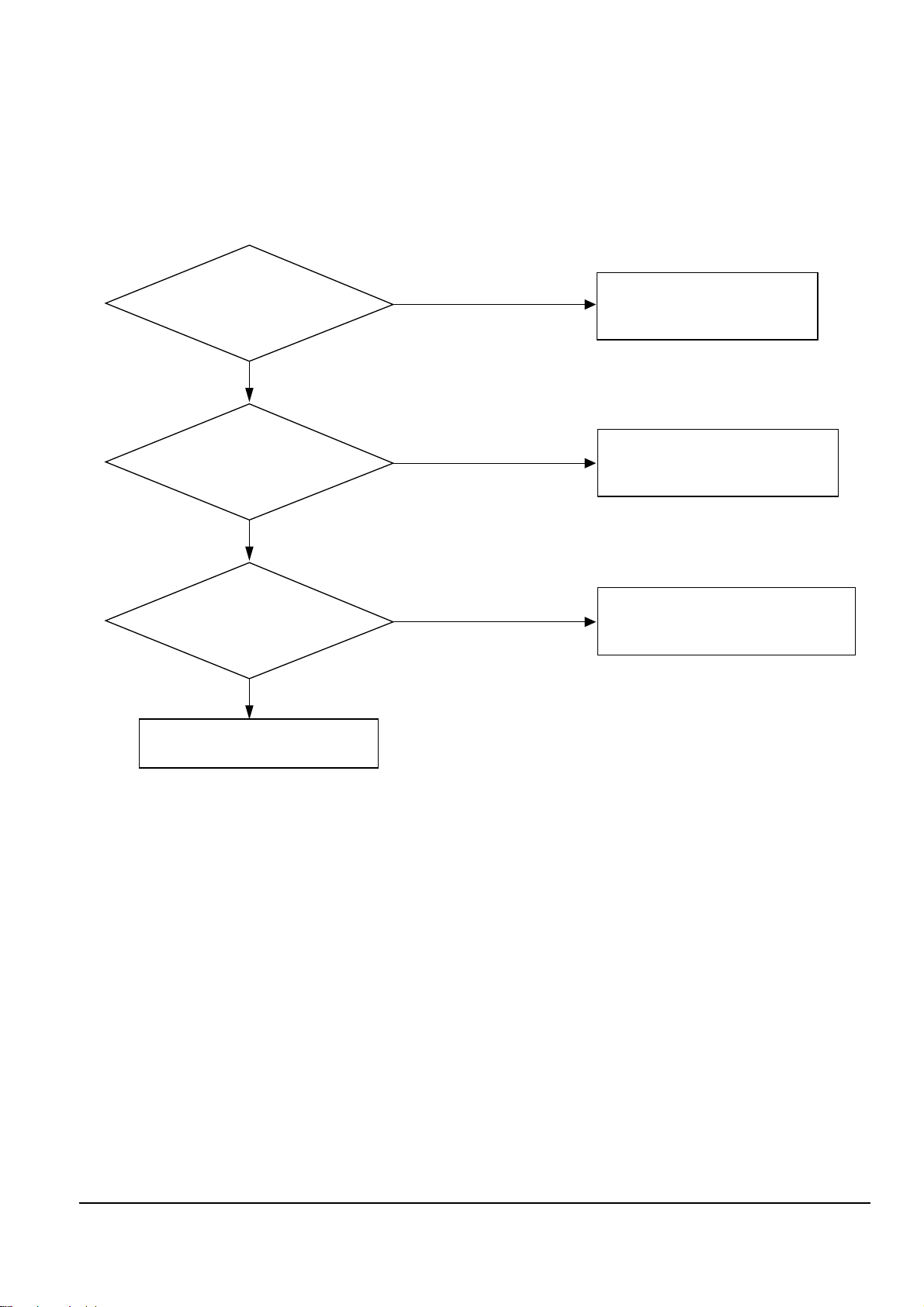
6-3 CD
6-3-1 Disc Revolution Malfunction
Troubleshooting
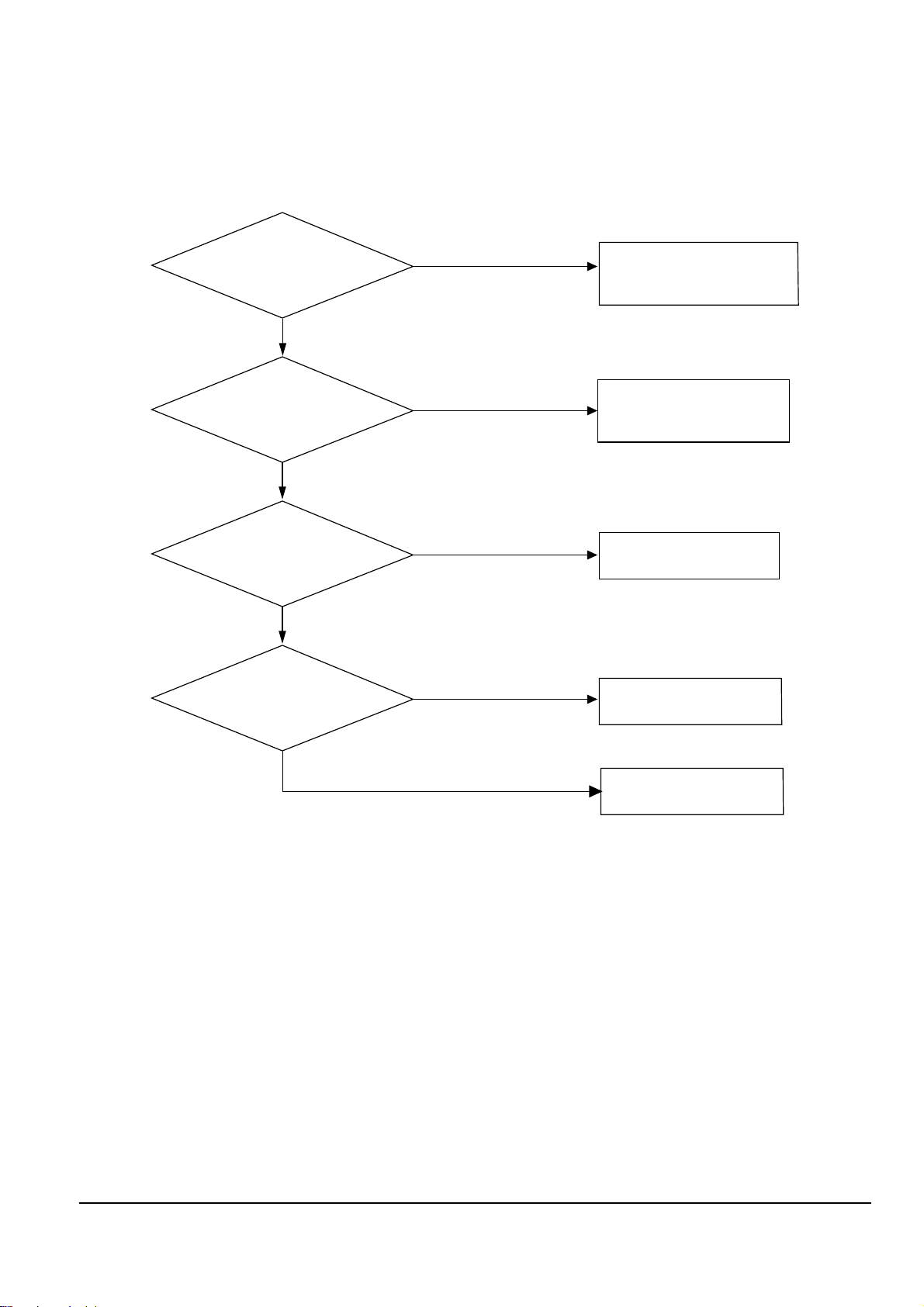
Samsung Electronics 6-7
Troubleshooting
6-3-2 Audio Output Malfunction
Yes
AQ103L,R Base B+ ?
Is Mute selected ?
Headphone Jack short ?
Remove it with Remocon.
Replace Headphone jack
soldering condition.
Main PCB AIC101
(STK4121,4141,4181-Option)
pin no. 9,11,12,14
B+,B- circuits
Check the B+ power
source part in RD1(PBL403),
RC2,3 and RIC1.
Yes
Confirm for TR short
replace it.
Check if the output line is
short.
No
No
No
No
Yes
Yes
6-8 Samsung Electronics
Troubleshooting
O
Check voltage of PI1, CQ1 ?
O
Check oscillation of MX1, CX1 ?
O
O
There is no Video CD read in
X
Check connection of short
Check 8V output of Main PCB
X
X
Check oscillation
connection condition
& short
Check reset of MI1 pin50,
CI1 pin101?
Check µ-com of Main PCB
X
X
Check connection condition
& short
O
Check communication of
MI1,CI1 ?
O
Check commucation of
CI1,RI1,RI2,RI3 ?
Lead In Mode : check data input
of CI1 pin104,105,106
X
Check MI1,CI1 connection
X
Check CI1,RI1,RI2,RI3
connection & short
Check communication of MI1
pin3,33,34,42,43 ?
Check µ-com of Main PCB
X
X
Check connection of short
O
& short
6-4 Video CD
6-4-1 Load In Malfunction
 Loading...