


Preliminary
TO
DATE
SAMSUNG TFT-LCD
SAMSUNG TFT-LCD
MODEL NO. : LTN170CT10-***
MODEL NO. : LTN170CT10-***
NOTE :
NOTE : Surface type [ Glare ]
www.jxlcd.com
:
: June. 29, 2009.
www.jxlcd.com
Any Modification of Spec is not allowed without SEC’ permission
SAMSUNG ELECTRONICS CO., LTD.
Samsung Secret
Doc.No. Rev.No
LTN170CT10-
04-P00-G-090629
Page
/ 28
1
CONTENTS
Preliminary
Revision History
General Description
1. Absolute Maximum Ratings
1.1 Absolute Ratings of environment
1.2 Electrical Absolute Ratings
2. Optical Characteristics
3. Electrical Characteristics
3.1 TFT LCD Module
3.2 Backlight Unit
4. Block Diagram
4.1 TFT LCD Module
4.2 Backlight Unit
5. Input Terminal Pin Assignment
5.1 Input Signal & Power
5.2 LVDS Interface
5.3 Backlight Unit
5.4 Timing Diagrams of LVDS For Transmitting
www.jxlcd.com
www.jxlcd.com
5.5 Input Signals, Basic Display Colors and Gray Scale of Each Color.
5.6 Pixel format
- - - - - - - - - - - - - - - - - - - ( 3 )
- - - - - - - - - - - - - - - - - - - ( 4 )
- - - - - - - - - - - - - - - - - - - ( 5 )
- - - - - - - - - - - - - - - - - - - ( 7 )
- - - - - - - - - - - - - - - - - - - ( 10 )
- - - - - - - - - - - - - - - - - - - ( 13 )
- - - - - - - - - - - - - - - - - - - ( 14 )
6. Interface Timing
6.1 Timing Parameters
6.2 Timing Diagrams of interface Signal
6.3 Power ON/OFF Sequence
7. Mechanical outline dimension
8. General Precaution
Samsung Secret
Doc.No. Rev.No
LTN170CT10-
- - - - - - - - - - - - - - - - - - - ( 20 )
- - - - - - - - - - - - - - - - - - - ( 23 )
-- - - - - - - - - - - - - - - - - - ( 28 )
04-P00-G-090629
Page
/ 28
2
REVISION HISTORY
REVISION HISTORY
LTN170CT10-G01 Model spec was issued first.AllP00June. 29. 2009
Preliminary
SummaryPageRevision No.Date
www.jxlcd.com
www.jxlcd.com
Samsung Secret
Doc.No. Rev.No
LTN170CT10-
04-P00-G-090629
Page
/ 28
3
Preliminary
GENERAL DESCRIPTION
DESCRIPTION
LTN170CT10-G01 is a color active matrix TFT (Thin Film Transistor) liquid crystal display
(LCD) that uses amorphous silicon TFT as a switching devices. This model is composed of
a TFT LCD panel, a driver circuit and a backlight system. The resolution of a 17.0" contains
1920 x 1200 pixels and can display up to 262,144 colors. 6 O'clock direction is the optimum
viewing angle.
FEATURES
• High contrast ratio
• Wide UXGA (1920x1200 pixels) resolution
• Low power consumption
• DE (Data enable) only mode.
• 3.3V LVDS Interface
• On board EDID chip
• LED BLU Structure
• Pb free / Halogen free / As free
APPLICATIONS
• Notebook PC
• If the usage of this product is not for PC application, but for others, please contact SEC
www.jxlcd.com
GENERAL INFORMATION
Pixel pitch
www.jxlcd.com
367.2(H) x 229.5(V) (17.0”diagonal)Display area
a-si TFT active matrixDriver element
262,144Display colors
1920 x 1200 (Wide UXGA )Number of pixel
RGB vertical stripePixel arrangement
0.19125(H) x 0.19125(V)
mm
pixel
mm
NoteUnitSpecificationItem
Normally WhiteDisplay Mode
Haze 0, HARD-COATING 3HSurface treatment
Samsung Secret
Doc.No. Rev.No
LTN170CT10-
04-P00-G-090629
Page
ARC7
/ 28
4
Mechanical Information
Preliminary
Module
size
Note (1) Measurement condition of outline dimension
. Equipment : Vernier Calipers
. Push Force : 500g ⋅f (minimum)
1. ABSOLUTE MAXIMUM RATINGS
1.1 ENVIRONMENTAL ABSOLUTE RATINGS
Storage temperate
Operating temperate
(Temperature of glass surface)
STG
OPR
Max.
379.6
244.9
4.2
565
NoteUnitTyp.Min.Item
mm379.3379.0Horizontal (H)
mm244.6244.3Vertical (V)
(1)mm3.9-Depth (D)
g560-Weight
NoteUnitMax.Min.SymbolItem
(1)°C60-20 T
(1)°C500T
(2),(4)G240-SnopShock ( non-operating )
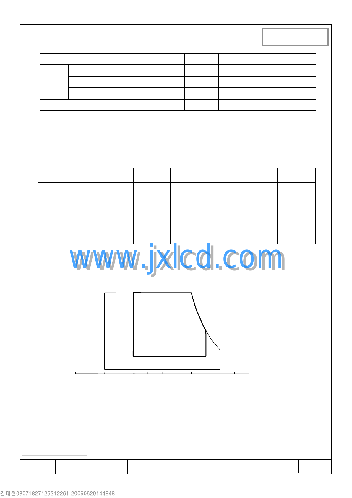
Note (1) Temperature and relative humidity range are shown in the figure below.
95 % RH Max. (40 °C ≥ Ta)
www.jxlcd.com
www.jxlcd.com
Maximum wet - bulb temperature at 39 OC or less. (Ta > 40 °C ) No condensation
100
-40 -20 0 20 40 60 80
Relative Humidity ( %RH)
90
80
60
40
20
Operating Range
Storage Range
5
0
( 40,90 )
( 50,50.4 )
( 60,27.7 )
Temperature (OC)
(2) 2ms, half sine wave, one time for ±X, ±Y, ± Z.
(3) 5 - 500 Hz, random vibration, 30min for X, Y, Z.
(4) At testing Vibration and Shock, the fixture in holding the Module to be tested have to be
hard and rigid enough so that the Module would not be twisted or bent by the fixture.
(5) If product is used for extended time excessively or exposed to high temperatures for extended time,
there is a possibility of wide viewing angle film damage which could affect visual characteristics
(3),(4)G2.41-VnopVibration (non-operating)
.
Samsung Secret
Doc.No. Rev.No
LTN170CT10-
04-P00-G-090629
Page
/ 28
5
1.2 ELECTRICAL ABSOLUTE RATINGS
(1) TFT LCD MODULE
Preliminary
VDD=3.3V, V
Power Supply Voltage
Logic Input Voltage
Note (1) Within Ta (25 ± 2 °C )
(2) BACK-LIGHT UNIT
LED Current
LED Voltage
Note 1) Permanent damage to the device may occur if maximum values are exceeded
Functional operation should be restricted to the conditions described under normal operating conditions.
L
L
DD
IN
SS
= GND = 0V
NoteUnitMax.Min.SymbolItem
(1)VVDD+ 0.3VDD- 0.3V
(1)VVDD+ 0.3VDD- 0.3V
Ta = 25 ± 2 °C
NoteUnitMax.Min.SymbolItem
(1)mA22.5-I
(1)V3.62.8V
www.jxlcd.com
www.jxlcd.com
Samsung Secret
Doc.No. Rev.No
LTN170CT10-
04-P00-G-090629
Page
/ 28
6
Preliminary
2. OPTICAL CHARACTERISTICS
The following items are measured under stable conditions. The optical characteristics
should be measured in a dark room or equivalent state with the methods shown in Note (5).
Measuring equipment : TOPCON SR-3
Contrast Ratio
(center)
Response Time at Ta
( Rising + Falling )
Average Luminance
of White (160 Points)
Red
Color
Chromaticity
( CIE )
Green
Blue
www.jxlcd.com
www.jxlcd.com
White
* Ta = 25 ± 2 °C, VDD=3.3V, fv= 60Hz, f
RT
AVE
R
X
R
Y
G
X
G
Y
B
X
B
Y
X
Y
Normal
Viewing
Angle
φ = 0
θ = 0
DCLK
= 78.97MHz, IL= 22.5mA
Unit
-
2016T
2
-250230YL,
0.6600.6400.620
0.3570.3370.310
0.3300.3100.290
0.6350.6150.595
0.1700.1500.130
0.0800.0600.040
0.3290.3130.297W
0.3450.3290.313W
cd/m
-
NoteMaxTyp.Min.ConditionSymbolItem
(1), (2), (5)-600400CR
(1), (3)
IL=22.5mA
(1), (4)
(1), (5)
SR-3
θ
L
Hor.
Viewing
Angle
160 Points
White Variation
Samsung Secret
Doc.No. Rev.No
LTN170CT10-
Ver.
H
CR ≥ 10
H
L
L
7065
7065θ
6050φ
6050φ
04-P00-G-090629
Degrees
%
Page
(1), (5)
SR-3
(6)-TBDδ
7
/ 28

Note 1) Definition of Viewing Angle : Viewing angle range(10
Normal Line
o
φ = 0
,
θ = 0
θ
L
φ
H
θL =90
φ
o
x
L
≤≤≤≤
o
C/R)
θ
R
Preliminary
12 O’clock
y
direction
φH= 90
o
6 O’clock
direction
φL= 90
Note 2) Definition of Contrast Ratio (CR) : Ratio of gray max (Gmax) ,gray min (Gmin)
Note 3) Definition of Response time :
Display data
Optical
Response
o
at center points (7)
CR = Luminance at Gmax / Luminance at Gmin
White(TFT OFF) White(TFT OFF)
www.jxlcd.com
www.jxlcd.com
100%
90%
10%
0%
T
R
Black(TFT ON)
x'y'
θR=90
T
F
o
Note 4) Definition of Average Luminance of White
Y
= SUM(L1:L160) / 160
L,AVE
where L1 to L160 are the luminance values measured at point #1 to #160.
Samsung Secret
Doc.No. Rev.No
LTN170CT10-
04-P00-G-090629
Page
Time
/ 28
8
Preliminary
Note 5) After stabilizing and leaving the panel alone at a given temperature for 30 min , the measurement
should be executed. Measurement should be executed in a stable, windless,and dark room.
30 min after lighting the backlight. This should be measured in the center of screen.
Lamp current : 6.0mA ( Inverter : SIC-130T )
Environment condition : Ta = 25 ± 2 °C
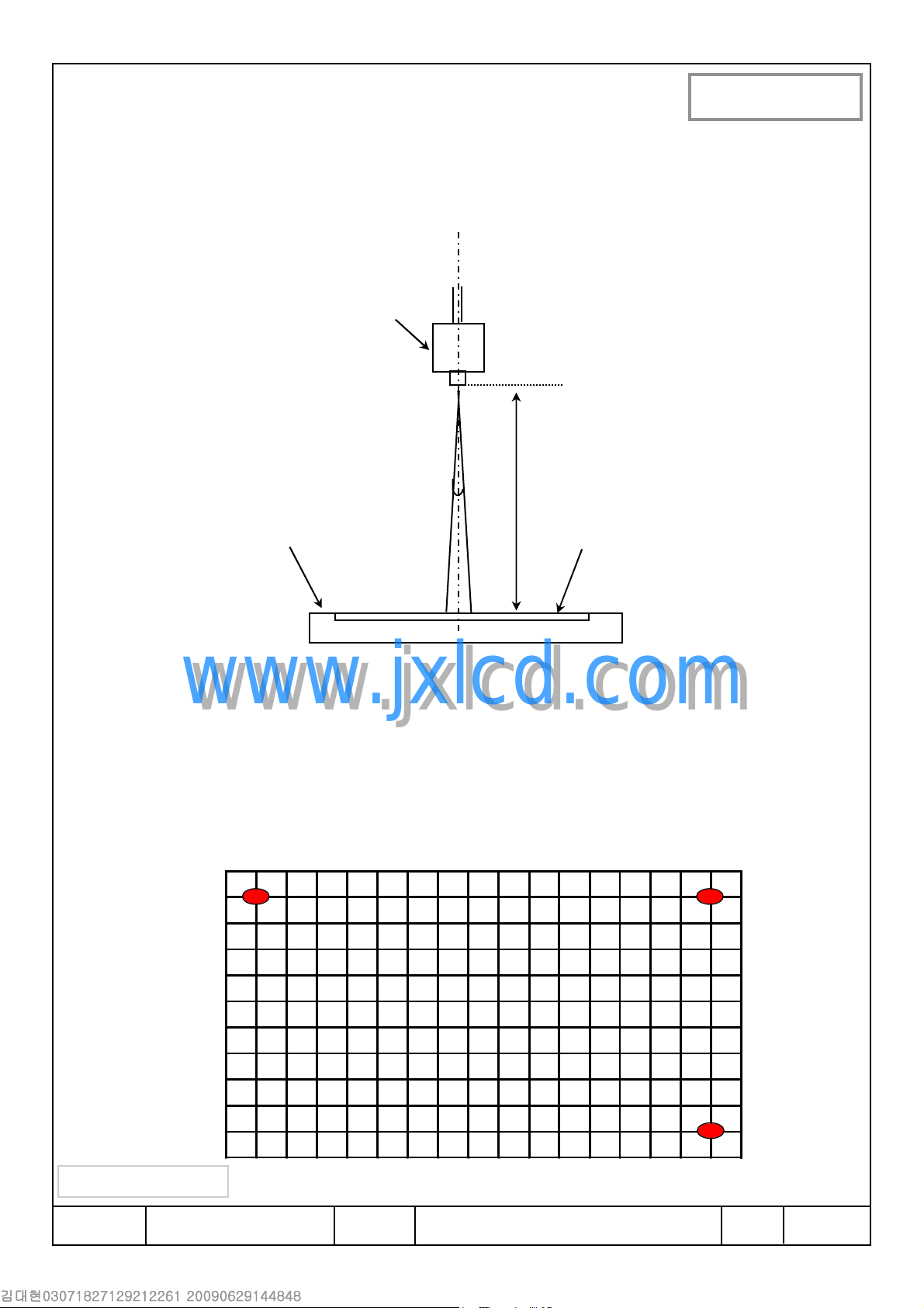
Photo-detector
( TOPCON SR-3 )
Field
= 2°
50 cm
TFT-LCD module
Center of the screen
www.jxlcd.com
www.jxlcd.com
Note 6) Definition of 160 points white variation (δ L )
δ L = 100% - (Lmax-Lmin)/Lmax
where, Lmax = max {Luminance values at 160 points},
Lmin = min {Luminance values at 160 points}
0 1/17L 16/17L L
0
1/11W
1
[ Optical characteristics measurement setup ]
LCD panel
16
10W/11
W
Samsung Secret
Doc.No. Rev.No
LTN170CT10-
04-P00-G-090629
160
Page
/ 28
9
3. ELECTRICAL CHARACTERISTICS
3.1 TFT LCD MODULE
Preliminary
Ta= 25 ± 2°C
NoteUnitMax.Typ.Min.SymbolItem
Voltage of Power Supply
Differential Input
Voltage for LVDS
Receiver Threshold
Hsync Frequency
Main Frequency
Rush Current
Current of Power
Supply
Note (1) Display data pins and timing signal pins should be connected. (GND = 0V )
www.jxlcd.com
www.jxlcd.com
(2) fV= 60Hz, f
(3) Power dissipation pattern
High
Low
White
DCLK
= 80.81MHZ, VDD= 3.3V , DC Current.
DD
IH
IL
H
DCLK
RUSH
I
DD
V3.63.33.0V
V
CM
= +1.2VmV+100--V
mV---100V
Hz-60-fvVsync Frequency
KHz-75-f
MHz-78.97-f
(4)A1.5--I
(2),(3)*amA430390350
(2),(3)*bmA550500450Mosaic
mA690630570Black
(2),(3)*cmA7206555901 dot inv.
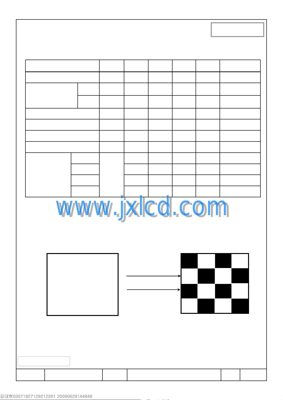
*a) White Pattern *b) Mosaic Pattern
VIEW AREA
Samsung Secret
Doc.No. Rev.No
LTN170CT10-
Display Brightest Gray Level
Display Darkest Gray Level
04-P00-G-090629
Page
10
/ 28