

Samsung LTN-140KT09-8 Datasheet
Approval
TO
DATE
SAMSUNG TFT-LCD
: IT Solution
: Sep. 19, 2011.
MODEL NO. : LTN140KT09-8
NOTE : Extension code [ -8** ]
www.jxlcd.com
www.jxlcd.com
→ LTN140KT09-8**
Surface type [ Anti-Glare ]
The information described in this SPEC is preliminary and can be changed without prior notice.
APPROVED BY :
Khan Kim
PREPARED BY :
Application Engineer Group
SAMSUNG ELECTRONICS CO., LTD.
Samsung Secret
Doc.No. Rev.No
00-A00-G-110919
Page
/ 37LTN140KT09-8
1
CONTENTS
Approval
Revision History
General Description
1. Absolute Maximum Ratings
1.1 Absolute Ratings of environment
1.2 Electrical Absolute Ratings
2. Optical Characteristics
3. Electrical Characteristics
3.1 TFT LCD Module
3.2 Backlight Unit
3.3 LED Driver
4. Block Diagram
4.1 TFT LCD Module
5. Input Terminal Pin Assignment
5.1 Input Signal & Power & Pin assignment
5.2 LVDS Interface
5.3 Timing Diagrams of LVDS For Transmitting
5.4 Input Signals, Basic Display Colors and Gray Scale of Each Color.
5.5 Pixel format
- - - - - - - - - - - - - - - - - - - ( 3 )
- - - - - - - - - - - - - - - - - - - ( 4 )
- - - - - - - - - - - - - - - - - - - ( 5 )
- - - - - - - - - - - - - - - - - - - ( 7 )
- - - - - - - - - - - - - - - - - - - ( 10 )
- - - - - - - - - - - - - - - - - - - ( 13 )
- - - - - - - - - - - - - - - - - - - ( 14 )
6. Interface Timing
6.1 Timing Parameters
6.2 Timing Diagrams of interface Signal
6.3 Power ON/OFF Sequence
7. Outline Dimension
8. Packing
9. Marking & Others
10. General Precaution
11. Appendix
Appendix A. EDID
Appendix B. MTBF Data
Appendix C. Safety Approval
Appendix D. Pogo Test Result
Appendix E. Key Part List
Appendix F. Impedance Test Result
www.jxlcd.com
www.jxlcd.com
- - - - - - - - - - - - - - - - - - - ( 21 )
- - - - - - - - - - - - - - - - - - - ( 23 )
-- - - - - - - - - - - - - - - - - -- ( 24 )
-- - - - - - - - - - - - - - - - - -- ( 25 )
-- - - - - - - - - - - - - - - - - - -( 27 )
-- - - - - - - - - - - - - - - - - - -( 30 )
Samsung Secret
Doc.No. Rev.No
00-A00-G-110919
Page
/ 37LTN140KT09-8
2
SPEC REVISION HISTORY
Approval
Date Revision No. Page
July. 04, 2011 P00 All The preliminary specification of LTN140KT09-8 was issued first.
Aug. 19, 2011 A00 All The approval specification was issued first.
Summary
www.jxlcd.com
www.jxlcd.com
CODE REVISION HISTORY
Date Model. Revision No. Summary MP or EOL
July. 04, 2011
LTN140KT09
801 Basic model From August. 2011 ~
Samsung Secret
Doc.No. Rev.No
00-A00-G-110919
Page
/ 37LTN140KT09-8
3
Approval
GENERAL DESCRIPTION
DESCRIPTION
LTN140KT09 is a color active matrix TFT (Thin Film Transistor) liquid crystal display
(LCD) that uses amorphous silicon TFT as switching devices. This model is composed of a
TFT LCD panel, a driver circuit and a backlight unit. The resolution of a 14.0" contains
1600X900pixels and can display up to 16.2M colors. 6 O'clock direction is the optimum
viewing angle.
FEATURES
• High contrast ratio
• HD+ (1600 x 900 pixels ) resolution
• Fast Response
• LED Back Light with embedded LED Driver
• DE (Data enable) only mode
• 3.3V LVDS Interface
• Onboard EEDID chip
• Green product (RoHS compliant)
• APS function
• 6bit-FRC
APPLICATIONS
• Notebook PC
• If the usage of this product is not for PC application, but for others, please contact SEC
www.jxlcd.com
GENERAL INFORMATION
Display area
Driver element
Display colors
Number of pixel
Pixel arrangement
Pixel pitch
www.jxlcd.com
Item Specification Unit Note
309.6H) x 174.15(V) ( 14.0” diagonal ) mm
a-Si TFT active matrix
16.2M
1600 x 900 pixel
RGB vertical stripe
0.1935(H) x 0.1935(V) (TYP.) mm
Display Mode
Surface treatment
Samsung Secret
Doc.No. Rev.No
Normally white
Haze 25%, Hard-Coating 3H Anti-glare
00-A00-G-110919
Page
/ 37LTN140KT09-8
4
Mechanical Information
Item Min. Typ. Max. Unit Note
Horizontal (H) 323 323.5 324 mm
Approval
Module
size
Note (1) Measurement condition of outline dimension
Vertical (V)
Depth (D) - - 4.0 mm (1) Body area
Weight - - 355 g
. Equipment : Bernier Calipers
. Push Force : 750 ± 250 g f
191.4 191.9 192.4 mm Module ~ Module
204.4 204.9 205.4 mm Outsize with Frange
1. ABSOLUTE MAXIMUM RATINGS
1.1 ENVIRONMENTAL ABSOLUTE RATINGS
Item Symbol Min. Max. Unit Note
Storage temperate TSTG -20 60 C (1)
Operating temperate
(Temperature of glass surface)
Shock ( non-operating ) Snop - 240 G (2),(4)
Vibration (non-operating) Vnop - 2.41 G (3),(4)
TOPR 0 50 C (1)
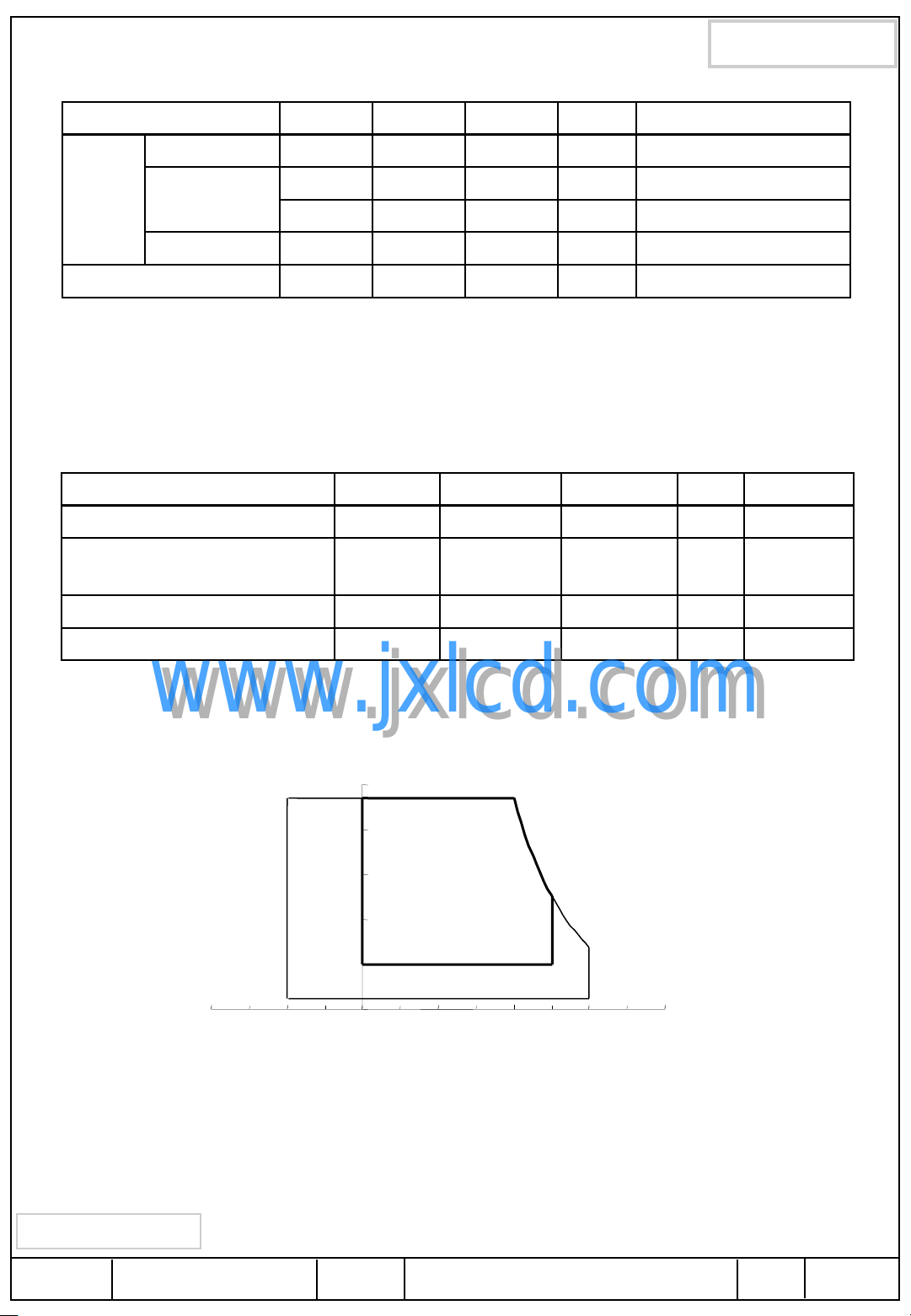
Note (1) Temperature and relative humidity range are shown in the figure below.
95 % RH Max. (40 C Ta)
www.jxlcd.com
www.jxlcd.com
Maximum wet - bulb temperature at 39 OC or less. (Ta 40 C ) No condensation
Relative Humidity ( %RH)
100
90
80
60
Operating Range
40
20
( 40,90 )
( 50,50.4)
( 60,27.7)
Storage Range
5
-40 -20 0 20 40 60 80
0
Temperature (OC)
(2) 2ms, half sine wave, one time for X, Y, Z.
(3) 5 - 500 Hz, random vibration, 30min for X, Y, Z.
(4) At testing Vibration and Shock, the fixture in holding the Module to be tested have to be
hard and rigid enough so that the Module would not be twisted or bent by the fixture.
Samsung Secret
Doc.No. Rev.No
00-A00-G-110919
Page
/ 37LTN140KT09-8
5
1.2 ELECTRICAL ABSOLUTE RATINGS
(1) TFT LCD MODULE
Item Symbol Min. Max. Unit Note
Power Supply Voltage VDD VDD - 0.3 VDD + 0.3 V (1)
Logic Input Voltage VIN VDD - 0.3 VDD + 0.3 V (1)
Note (1) Within Ta (25 2 C )
(2) BACK-LIGHT UNIT
Item Symbol Min. Typ. Max. Unit Note
Approval
VDD =3.3V, VSS = GND = 0V
Ta = 25 2 C , Duty = 100%
LED Current I
LED Voltage F
Note (1) Permanent damage to the device may occur if maximum values are exceeded
Functional operation should be restricted to the conditions described under normal operating conditions.
www.jxlcd.com
www.jxlcd.com
L
L
- 25 - mA (1)
3.0 3.2 3.4 V (1)
Samsung Secret
Doc.No. Rev.No
00-A00-G-110919
Page
/ 37LTN140KT09-8
6
Approval
2. OPTICAL CHARACTERISTICS
The following items are measured under stable conditions. The optical characteristics
should be measured in a dark room or equivalent state with the methods shown in Note (5).
Measuring equipment : TOPCON SR-3
* Ta = 25 2 C, VDD=3.3V, fv= 60Hz, fDCLK = 50.2MHz, IF = 25mA
Item Symbol Condition Min. Typ. Max Unit Note
Contrast Ratio
(5 Points)
Response Time at Ta
( Rising + Falling )
Average Luminance
of White (5 Points)
Red
Green
www.jxlcd.com
Color
Chromaticity
( CIE )
www.jxlcd.com
Blue
CR
TRT - 16 25 msec (1), (3)
YL,AVE 255 300 - cd/m
Normal
RX
RY
GX
GY
BX
BY
Viewing
Angle
= 0
= 0
300 - - - (1), (2), (5)
IF=25mA
(1), (4)
(1), (5)
SR-3
TYP
-0.03
0.575
0.345
0.330
0.558
0.160
0.120
TYP
+0.03
2
-
WX
White
WY
L
Hor.
Viewing
Angle
Ver.
13 Points
White Variation
Color Gamut CG - 45 - %
Samsung Secret
R
H
L
L
CR 10
At center
Doc.No. Rev.No
0.313
0.329
40
40
10
25
- - 2.0 - (6)
00-A00-G-110919
45
45
15
30
-
-
Degrees
-
-
(1), (5)
SR-3
Page
/ 37LTN140KT09-8
7
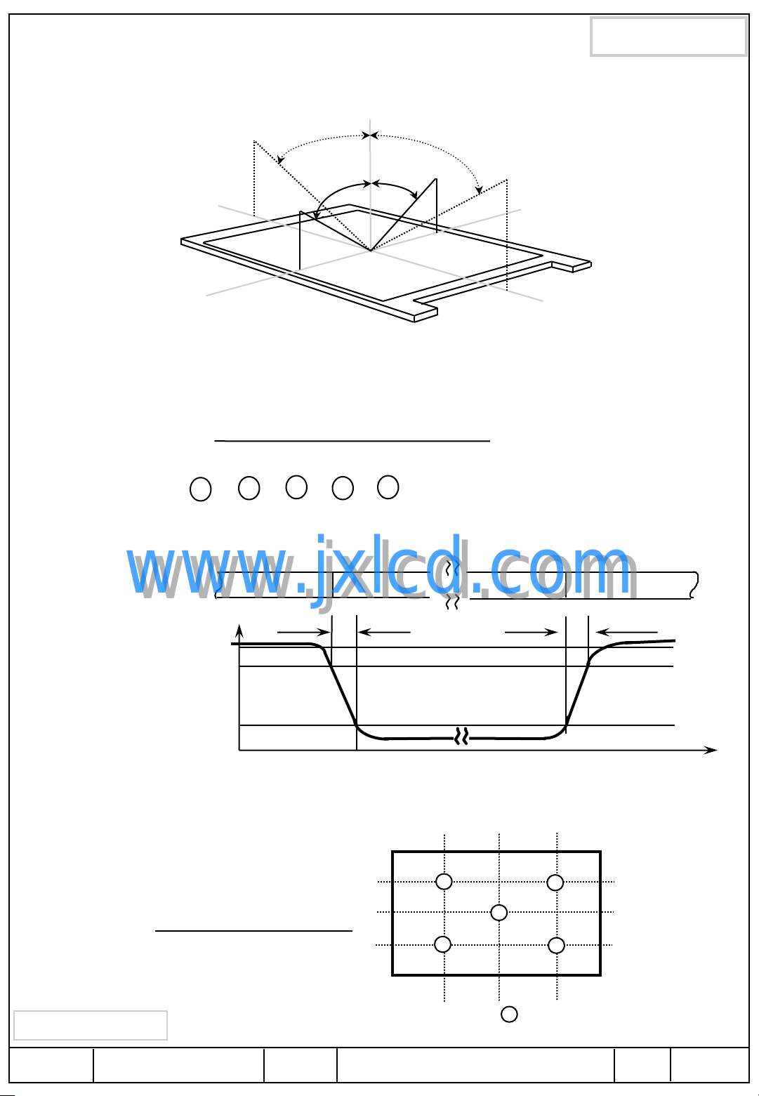
Note 1) Definition of Viewing Angle : Viewing angle range(10 C/R)
Normal Line
o
,
= 0
o
R
= 0
L
L
L
=90
o
x
H
Approval
12 O’clock
y
direction
= 90
H
o
6 O’clock
direction
Note 2) Definition of Contrast Ratio (CR) : Ratio of gray max (Gmax) ,gray min (Gmin)
at 5 points(4, 5, 7, 9, 10)
Note 3) Definition of Response time :
Display data
Optical
Response
o
= 90
L
CR(4) + CR(5) + CR(7) + CR(9) + CR(10)
CR =
Points : , , , , at the figure of Note (6).
www.jxlcd.com
www.jxlcd.com
4 9
100%
90%
10%
0%
5
White(TFT OFF) White(TFT OFF)
7
5
10
Black(TFT ON)
TR
x'y'
=90
R
TF
o
Note 4) Definition of Average Luminance of White : measure the luminance of white at 5 points.
25% 50% 75%
Average Luminance of White ( YL,AVE )
YL4 + YL5 + YL7 + YL9 + YL10
YL,AVE =
5
Samsung Secret
Doc.No. Rev.No
00-A00-G-110919
10
9
7
5
4
: test point
Time
VIEW AREA
25%
50%
75%
(lines)
Page
/ 37LTN140KT09-8
8
Approval
Note 5) After stabilizing and leaving the panel alone at a given temperature for 30 min , the measurement
should be executed. Measurement should be executed in a stable, windless,and dark room.
30 min after lighting the backlight. This should be measured in the center of screen.
IF current : 25 mA
Environment condition : Ta = 25 2 C
Photo-detector
( TOPCON SR-3 )
Field = 2
50 cm
TFT-LCD module
Center of the screen
[ Optical characteristics measurement setup ]
www.jxlcd.com
www.jxlcd.com
Note 6) Definition of 13 points white variation ( L ), CR variation( CVER ) [ ~ ]
Maximum luminance of 13 points
L =
10mm
Minimum luminance of 13 points
10mm
25% 50%
13 12
10
75%
9
LCD panel
1 13
10mm
11
25%
8
5
3
10mm
Samsung Secret
Doc.No. Rev.No
7
4
2
00-A00-G-110919
6
50%
75%
1
: test point
Page
/ 37LTN140KT09-8
9
3. ELECTRICAL CHARACTERISTICS
Approval
3.1 TFT LCD MODULE
Item Symbol Min. Typ. Max. Unit Note
Voltage of Power Supply VDD 3.0 3.3 3.6 V
Differential Input
Voltage for LVDS
Receiver Threshold
Vsync Frequency fv - 60 - Hz
Main Frequency fDCLK - 50.2 - MHz 2CH
Rush Current IRUSH - - 1.5 A (4)
Current of Power
Supply
High VIH - - +100 mV VCM = +1.2V
Low VIL -100 - - mV
White
Mosaic -
IDD
Black -
V.Stripe - 540
-
330 -
330 -
330 -
-
Ta= 25 2C
mA (2),(3)*a
mA
mA (2),(3)*b
mA (2),(3)*c
Note (1) Display data pins and timing signal pins should be connected.( GND = 0V )
(2) fV = 60Hz, fDCLK = 50.2MHZ, VDD = 3.3V , DC Current.
(3) Power dissipation pattern
www.jxlcd.com
*a) White Pattern
www.jxlcd.com
*c) Black
Display Brightest Gray Level
Display Darkest Gray Level
*b) Mosaic Pattern
Samsung Secret
Doc.No. Rev.No
00-A00-G-110919
Page
10
/ 37LTN140KT09-8
d) V.Stripe
4) Rush current measurement condition
Approval
CONTROL SIGNAL
(HIGH to LOW)
3.3V
M1
2SK1059
VDD ( LCD INPUT)
R1
47K
R2
www.jxlcd.com
www.jxlcd.com
12V
C3
1uF
VDD rising time is 470us
1K
R3
47K
M2
2SK1399
C2
10000pF
0.9VDD
FUSE
C1
1uF
3.3V
0.1VDD
GND
Samsung Secret
Doc.No. Rev.No
470us
00-A00-G-110919
Page
11
/ 37LTN140KT09-8
Approval
3.2 BACK-LIGHT UNIT
Item Symbol Min. Typ. Max. Unit Note
LED Forward Current IF - 25 - mA
LED Forward Voltage VF 3.0 3.2 3.4 V
LED Array Voltage VP 27 28.8 30.6 V VF X 9 LEDs
LED Counts - 36 - EA
Operating Life Time Hr 10,000 - - Hour (1)
Note (1) Life time (Hr) of LEDs can be defined as the time in which it continues to operate under the
condition Ta= 25 2 C and IF = 25mA until one of the following event occurs.
1. When the brightness becomes 50% or lower than the original.
3.3 LED Driver
- On board LED Driver (Manufacturer : Richtek)
Ta= 25 2 C
Ta= 25 2 C
Item Symbol Min. Typ. Max. Unit Note
Input Voltage Vin 6 12 24 V
Input Current I - 310 - mA
consumption
EN Control Level
PWM Control Level
External PWM
Dimming Control
Frequency (BLIM)
PWM duty ratio D
www.jxlcd.com
www.jxlcd.com
BL power
Pin
ON 1.5 3.3 5.0 V
OFF 0 0 0.5 V
ON 1.5 3.3 5.0 V
OFF 0 0 0.1 V
FBLIM 0.20 - 10 kHz
- - 0.85 W @ 60nit
- - 3.55 W @ Max
5 - 100 %
10 - 100 %
Vin=7~20V,
BLIM=PWM
0V~3.3V
PWM Freq. :
200Hz~10KHz
PWM Freq. :
1KHz~10KHz
Note - Test Equipment : Fluke 45
Samsung Secret
Doc.No. Rev.No
00-A00-G-110919
Page
12
/ 37LTN140KT09-8
 Loading...