

DATE : July. 14, 2010.
SAMSUNG TFT-LCD
SAMSUNG TFT-LCD
MODEL NO. : LTN097XL01-A01
MODEL NO. : LTN097XL01-A01
Approval
NOTE : Extension code [ -A01 ]
www.jxlcd.com
www.jxlcd.com
Any modification of Spec is not allowed without SEC’s permission
APPROVED BY :
PREPARED BY :
Application Engineer part 1, LCD Business
→ LTN097XL01-A01
Surface type [ Glare ]
Andrew, Cho
SAMSUNG ELECTRONICS CO., LTD.
Samsung Secret
Doc.No. Rev.No
04-A00-G-100714
Page
/ 25LTN097XL01-A01
1
CONTENTS
Approval
Revision History
General Description
1. Absolute Maximum Ratings
1.1 Absolute Ratings of environment
1.2 Electrical Absolute Ratings
2. Optical Characteristics
3. Electrical Characteristics
3.1 TFT LCD Module
3.2 Backlight Unit
4. Block Diagram
4.1 TFT LCD Module
4.2 LED Placement Structure
5. Input Terminal Pin Assignment
5.1 Input Signal & Power
5.2 LVDS Interface
5.3 Timing Diagrams of LVDS For Transmitting
5.4 Input Signals, Basic Display Colors and Gray Scale of Each Color.
www.jxlcd.com
www.jxlcd.com
5.5 Pixel format
- - - - - - - - - - - - - - - - - - - ( 3 )
- - - - - - - - - - - - - - - - - - - ( 4 )
- - - - - - - - - - - - - - - - - - - ( 5 )
- - - - - - - - - - - - - - - - - - - ( 7 )
- - - - - - - - - - - - - - - - - - - ( 10 )
- - - - - - - - - - - - - - - - - - - ( 13 )
- - - - - - - - - - - - - - - - - - - ( 14 )
6. Interface Timing
6.1 Timing Parameters
6.2 Timing Diagrams of interface Signal
6.3 Power ON/OFF Sequence
7. Outline Dimension
8. General Precaution
Samsung Secret
- - - - - - - - - - - - - - - - - - - ( 20 )
- - - - - - - - - - - - - - - - - - - ( 22 )
- - - - - - - - - - - - - - - - - - - ( 24 )
Doc.No. Rev.No
04-A00-G-100714
Page
/ 25LTN097XL01-A01
2
REVISION HISTORY
REVISION HISTORY
The Approval specification of LTN097XL01-A01 was issued first.AllA00Jul.14.2010
Approval
SummaryPageRevision No.Date
www.jxlcd.com
www.jxlcd.com
Samsung Secret
Doc.No. Rev.No
04-A00-G-100714
Page
/ 25LTN097XL01-A01
3
Approval
GENERAL DESCRIPTION
DESCRIPTION
LTN097XL01-A01 is a color active matrix TFT (Thin Film Transistor) liquid crystal display
(LCD) that uses amorphous silicon TFT as switching devices. This model is composed of a
TFT LCD panel, a driver circuit and a backlight system. The resolution of a 9.7" contains
1024 x 768 pixels and can display up to 262,144 colors. 6 O'clock direction is the Optimum
viewing angle.
FEATURES
• High contrast ratio, high aperture structure
• 1024 x 768 pixels resolution
• LED BLU Structure
• DE (Data enable) only mode.
• 3.3V LVDS Interface
• RoHS Compliance
• PB, Halogen Free Product
APPLICATIONS
• Notebook PC
• If the usage of this product is not for PC application, but for others, please contact SEC
GENERAL INFORMATION
www.jxlcd.com
www.jxlcd.com
196.608(H) X 147.456(V) (9.7”diagonal)Display area
a-si TFT active matrixDriver element
262,144Display colors
1024 x 768(XGA)Number of pixel
RGB vertical stripePixel arrangement
0.192(H) x 0.192(V) (TYP.)Pixel pitch
Normally Black, PLS modeDisplay Mode
mm
mm
NoteUnitSpecificationItem
4 : 3pixel
0.3TGlass Thickness
Haze 0, Hard-Coating 3HSurface treatment
Samsung Secret
Doc.No. Rev.No
04-A00-G-100714
Page
/ 25LTN097XL01-A01
4
Mechanical Information
Approval
Module
size
Note (1) Measurement condition of outline dimension
Vertical (V)
. Equipment : Vernier Calipers
. Push Force : 750g ⋅f (minimum)
1. ABSOLUTE MAXIMUM RATINGS
1.1 ENVIRONMENTAL ABSOLUTE RATINGS
Operating temperate
(Temperature of glass surface)
Max.
210.5
166.5
3.40
156
NoteUnitTyp.Min.Item
Outline with BracketMm210.2209.9Horizontal (H)
Module ~ PCBmm166.2165.9
(1)mm3.152.90Depth (D)
g151-Weight
NoteUnitMax.Min.SymbolItem
(1)°C60-20 TSTGStorage temperate
(1)°C500TOPR
(2),(4)G240-SnopShock ( non-operating )
Note (1) Temperature and relative humidity range are shown in the figure below.
95 % RH Max. (40 °C > Ta)
Maximum wet - bulb temperature at 39 OC or less. (Ta ≥ 40 °C ) No condensation
www.jxlcd.com
www.jxlcd.com
100
-40 -20 0 20 40 60 80
Relative Humidity ( %RH)
90
80
60
40
20
Operating Range
Storage Range
5
0
( 40,90 )
( 50,50.4 )
( 60,27.7 )
Temperature (OC)
(2) 2ms, half sine wave, one time for ±X, ±Y, ± Z.
(3) 5 - 500 Hz, random vibration, 30min for X, Y, Z.
(4) At testing Vibration and Shock, the fixture in holding the Module to be tested have to be
hard and rigid enough so that the Module would not be twisted or bent by the fixture.
(3),(4)G2.41-VnopVibration (non-operating)
Samsung Secret
Doc.No. Rev.No
04-A00-G-100714
Page
/ 25LTN097XL01-A01
5
1.2 ELECTRICAL ABSOLUTE RATINGS
(1) TFT LCD MODULE
Approval
Power Supply Voltage
Logic Input Voltage
BLU Operating Voltage
Note (1) Within Ta (25 ± 2 °C )
DD
DD
BLU
DD
DD
VDD=3.3V, V
DD
DD
+ 0.3V
+ 0.3V
– 0.3V
– 0.3V
SS
= GND = 0V
NoteUnitMax.Min.SymbolItem
(1)VV
(1)VV
(1)V19.216.8V
www.jxlcd.com
www.jxlcd.com
Samsung Secret
Doc.No. Rev.No
04-A00-G-100714
Page
/ 25LTN097XL01-A01
6
Approval
2. OPTICAL CHARACTERISTICS
The following items are measured under stable conditions. The optical characteristics
should be measured in a dark room or equivalent state with the methods shown in Note (5).
Measuring equipment : TOPCON BM-5A and PR-650
Contrast Ratio
(5 Points)
Response Time at Ta
( Rising + Falling )
Average Luminance
of White (5 Points)
Red
Color
Chromaticity
( CIE 1931)
Green
www.jxlcd.com
Blue
www.jxlcd.com
* Ta = 25 ± 2 °C, VDD=3.3V, fv= 60Hz, f
CR
RT
AVE
Normal
R
X
Y
X
Y
X
Y
Viewing
Angle
φ = 0
θ = 0
Typ
-0.03
0.605
0.345R
0.325G
0.570G
0.150B
0.125B
DCLK
=100 MHz, IL= 20 mA, 80% duty
Unit
Typ
+0.03
-
Msec
cd/m
-
(1), (2), (5)-900700
2
Measured
by PR-650
NoteMaxTyp.Min.ConditionSymbolItem
(1), (3)3530-T
(1), (4)-390350YL,
(1), (5)
Viewing
Angle
13 Points
White Variation
Samsung Secret
White
Hor.
Ver.
X
Y
θ
L
R
CR ≥ 10
H
L
L
0.313W
0.329W
-89-
-89-θ
-89-φ
-89-φ
Degrees
%-52-CGColor Gamut
-
(1), (5)
BM-5A
(6)1.54--δ
Doc.No. Rev.No
04-A00-G-100714
Page
/ 25LTN097XL01-A01
7
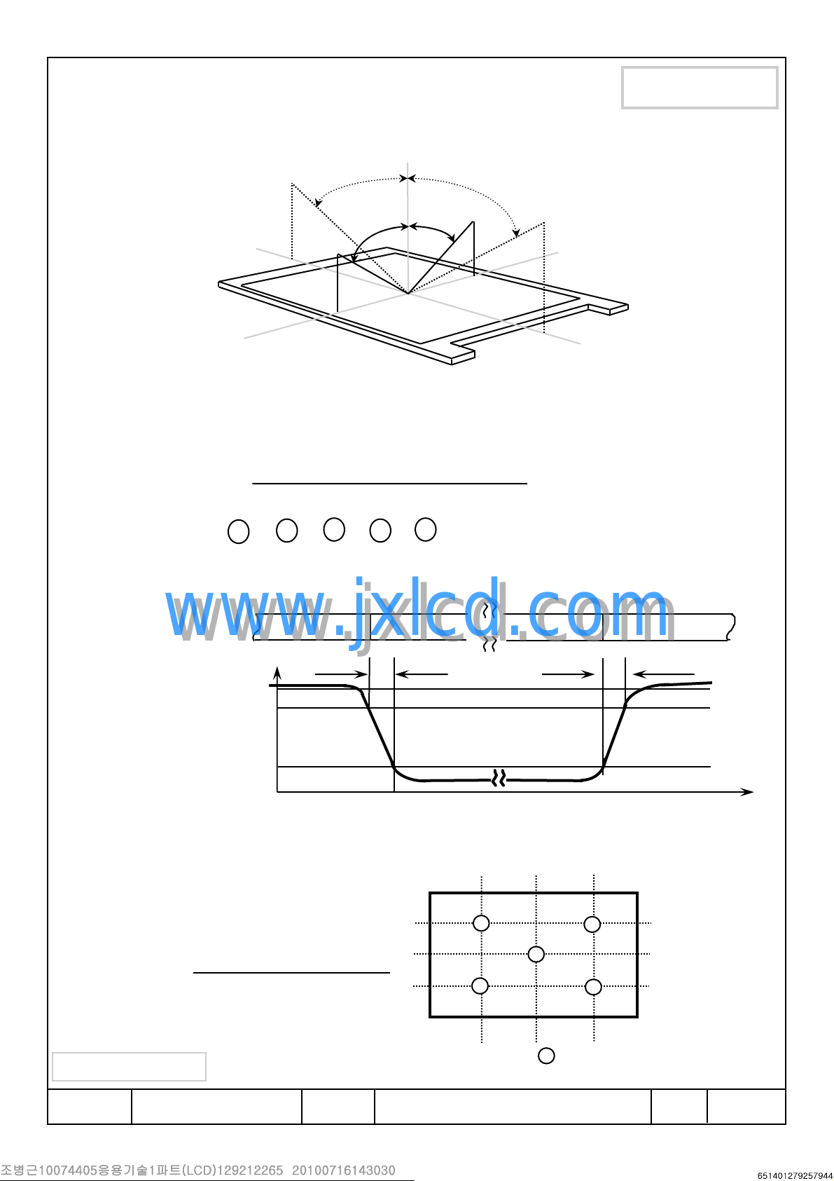
Note 1) Definition of Viewing Angle : Viewing angle range(10
Normal Line
o
φ = 0
,
θ = 0
θ
L
φ
H
θL =90
φ
o
x
L
≤≤≤≤
o
C/R)
θ
R
Approval
12 O’clock
y
direction
φH= 90
o
6 O’clock
direction
φL= 90
Note 2) Definition of Contrast Ratio (CR) : Ratio of gray max (Gmax) ,gray min (Gmin)
at 5 points(4, 5, 7, 9, 10)
Note 3) Definition of Response time :
Display data
Optical
Response
o
CR(4) + CR(5) + CR(7) + CR(9) + CR(10)
CR =
Points : , , , , at the figure of Note (6).
www.jxlcd.com
www.jxlcd.com
4 9
100%
90%
10%
0%
5
White(TFT OFF) White(TFT OFF)
7
5
10
Black(TFT ON)
T
R
x'y'
θR=90
T
F
o
Note 4) Definition of Average Luminance of White : measure the luminance of white at 5 points.
256 512 768
Average Luminance of White ( Y
YL4+ YL5+ YL7+ YL9+ Y
Y
L,AVE
=
Samsung Secret
Doc.No. Rev.No
5
L,AVE
)
L10
10
9
7
5
4
: test point
04-A00-G-100714
Time
VIEW AREA
150
300
450
(lines)
Page
/ 25LTN097XL01-A01
8
 Loading...