

Page 1
For Mujin Only
PRODUCT SPECIFICATION
(√ ) PRODUCT INFORMATION
( ) APPROVAL SPECIFICATION
This Product Information is subject to change after 3 months of issuing date
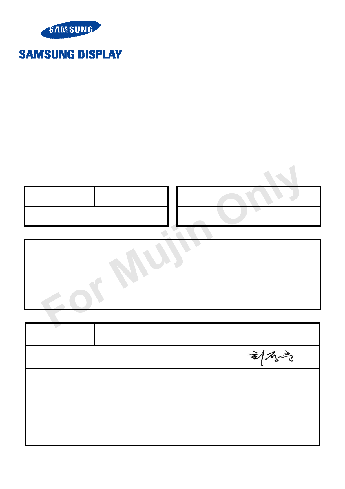
CUSTOMER 0XMLQ02DE//T
PROGRAM EXTENSION CODE &
CUSTOMER APPROVAL & FEEDBACK
ARPPROVED BY
PREPARED BY
05 / June / ’13 Ted Kim
05 / June / ’13 Kyle Choi
M270HL02
Ted Kim
Application Engineering Group
Samsung Display Co., Ltd.
Page 2
For Mujin Only
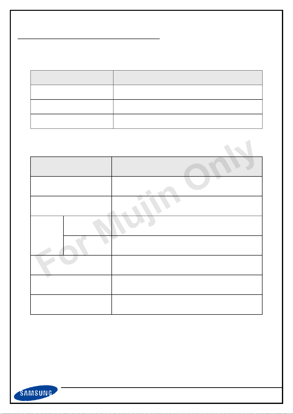
Product Configuration Approval Sheet
Description
Items
SAMSUNG DISPLAY
Content
Customer
Product Name LTM270HL02
Project Name
Customer System Configuration
Items
System Name
Purpose
Scalar
0XMLQ
Content
Standard MNT
-
IC
LED Driver
Input Interface
OS ( AIO)
Graphic Card (AIO)
Notice : Samsung product approval spec guarantee a above customer system.
-
-
-
-
P0.0
LTM270HL02
05. Jun. 2013
2
/35
Page 3
/
SAMSUNG DISPLAY
For Mujin Only
Contents
Revision History ----------------------------------------------------------------------------------- (4)
1. General Description ------------------------------------------------------------------------------ (5)
2. Absolute Maximum Ratings --------------------------------------------------------------------- (6)
3. Optical Characteristics --------------------------------------------------------------------------- (8)
4. Block Diagram ------------------------------------------------------------------------------------ (12)
5. Electrical Characteristics -------------------------------------------------------------------------- (13)
5.1 TFT LCD Module
5.2 Back Light Unit
5.3 LVDS Input Characteristics
5.4 Timing Parameters
5.5 Input Signals, Basic Display Colors and Gray Scale of Each Color
5.6 Power ON/OFF Sequence
5.7 Input Terminal Pin Assignment
6. Outline Dimension ------------------------------------------------------------------------------- (27)
7. Packing ------------------------------------------------------------------------------------------- (28)
8. General Precautions ------------------------------------------------------------------------------ (30)
8.1 Handling Precautions
8.2 Storage Precautions
8.3 Operation Precaution
8.4 Design Guide for System
35
P0.0
LTM270HL02
05. Jun. 2013
3
Page 4
/
For Mujin Only
Revision History
SAMSUNG DISPLAY
Version
P0.0
Date
5.June.,2013 All Product information
Page
Description
35
P0.0
LTM270HL02
05. Jun. 2013
4
Page 5
/
SAMSUNG DISPLAY
For Mujin Only
1. General Description
Overview
LTM270HL02-C is a color active matrix liquid crystal display (LCD) that uses amorphous
silicon TFT (Thin Film Transistor) as switching components. This model is composed of a
TFT LCD panel, a driver circuit and a back light unit. The resolution of a 27.0” is 1920 x
1080 (FHD) and this model can display up to 16.7 million colors.
Features
Application
- Workstation & Desktop monitors
- Display terminals for AV Products
- Monitors for Industrial machine
DE (Data Enable) only mode
LVDS (Low Voltage Differential Signaling) interface (2pixel/clock)
RoHS, Halogen Free
White LED Edge slim Backlight (1-side)
TCO 6.0 compliance
General Information
Items
Pixel Pitch
Active Display Area
Surface Treatment
Display Colors
Number of Pixels
Pixel Arrangement
Display Mode
AG type, Haze 25% , Hard coating (3H)
Specification Unit
0.1038(H) x 0.1038(W) mm
597.9(H) x 336.3(V) mm
16.7M (Hi-FRC) colors
1,920 x 1,080 pixel
RGB vertical stripe -
Normally Black(PLS mode) -
-
Luminance of White 300(Typ.)
Power Consumption
P0.0
Total (17.46W) (Typ.) ( Panel 2.46 W / BLU 15.00 W)
LTM270HL02
05. Jun. 2013
cd/㎡
W
5
35
Page 6
/
For Mujin Only
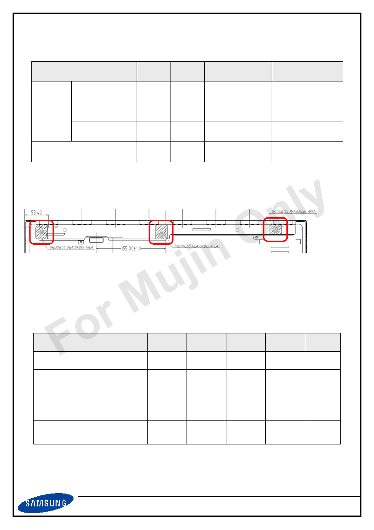
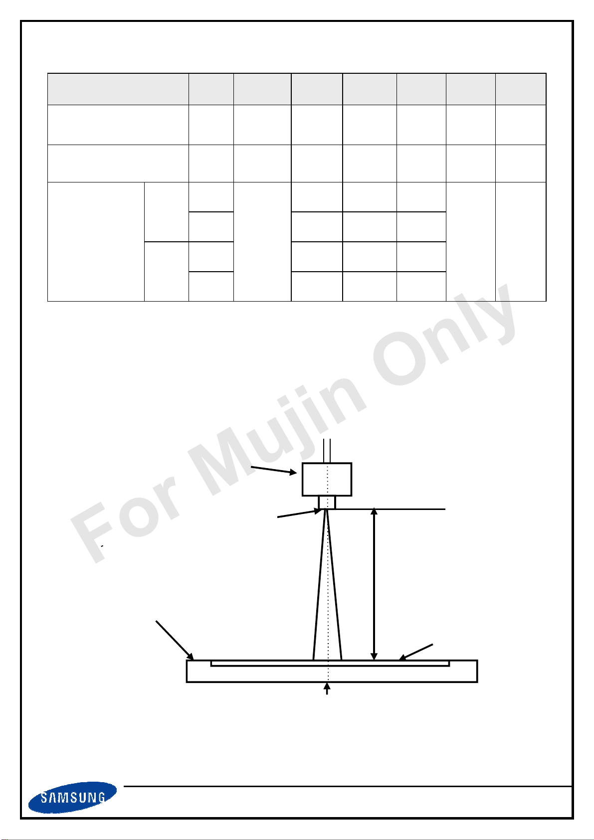
Mechanical Information
Item
Min.
SAMSUNG DISPLAY
Typ.
Max.
Unit
Note
Horizontal (H)
Module
Note (1) Mechanical tolerance is ± 0.5mm unless there is a special comment.
Note (2) The thickness measuring area please refer to below picture.
Measuring point to screw hole edge within 5mm.
size
Weight
Vertical (V)
Depth (D)
629.5 630.0 630.5 mm
367.7 368.2 368.7 mm
12.2
-
-
(3,200) g
mm
LCD module only
-
-
2. Absolute Maximum Ratings
If the condition exceeds maximum ratings, it can cause malfunction or unrecoverable damage
to the device.
Power Supply Voltage
Operating Temperature
Glass surface temperature
Note (1) Ta= 25 ± 2 °C
Item
Storage temperature
(Operation)
Symbol Min. Max. Unit
T
V
T
T
DD
OPR
STG
SUF
GND-0.5 6.5 V
0
-20
0
50
60
65
℃
℃
℃
Note
(1)
(2)
(3)
35
P0.0
LTM270HL02
05. Jun. 2013
6
Page 7
/
SAMSUNG DISPLAY
For Mujin Only
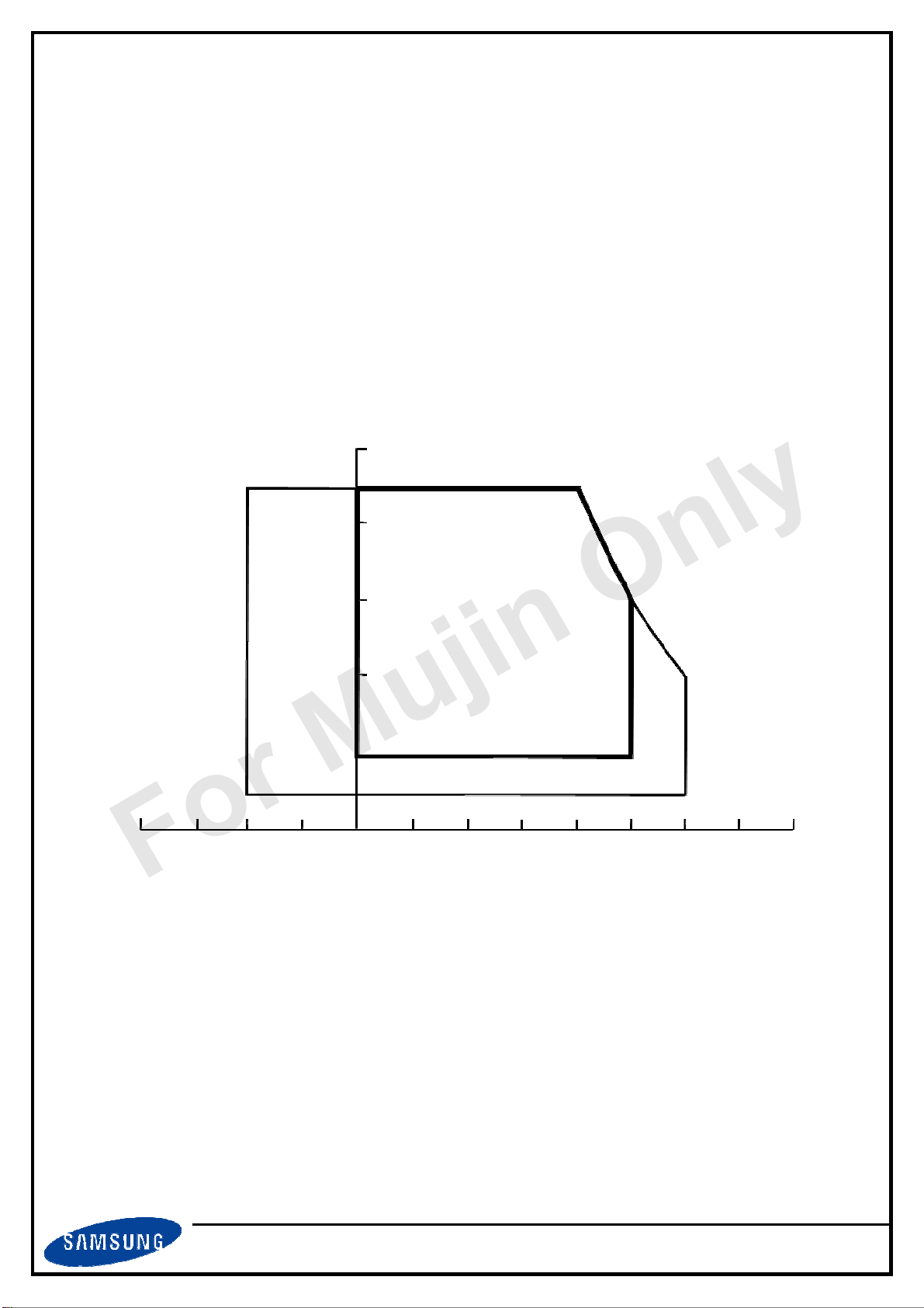
(2) Temperature and relative humidity range are shown in the figure below.
a. 90 % RH Max. (Ta ≤ 39 °C)
b. Maximum wet-bulb temperature at 39 °C or less. (Ta ≤ 39 °C)
c. No condensation.
(3) The maximum operating temperature of LCD module is defined with surface
temperature of active area. Under any condition, the maximum ambient operating
temperature should be keeping the surface of active area not any higher than 65 °C
Relative Humidity (% RH)
100
(39, 90)
90
80
60
Operating Range
40
20
(-20, 10)
-40
-20
10
0
Storage Range
20
40
(50, 50.4)
(60, 27.7)
Temperature (°C )
60
80
Fig. Temperature and Relative Humidity range
35
P0.0
LTM270HL02
05. Jun. 2013
7
Page 8
/
SAMSUNG DISPLAY
For Mujin Only
3. Optical Characteristics
The optical characteristics should be measured in a dark room or equivalent.
Measuring equipment : SR-3, RD-80S (TOPCON), EZ-Contrast (Eldim)
Item
(Ta = 25 ± 2°C, VDD=5V, fv= 60Hz, f
Symbol Condition Min. Typ. Max.
=67.3MHz, If =375mA)
DCLK
Unit
Note
Contrast Ratio
(Center of screen)
Response Time
Luminance of White
(Center of screen)
Brightness Uniformity
(9 Points)
Color
Chromaticity
(CIE 1931)
Red
Green
Blue
White
Red
C/R
G to G
Y
L
B
uni
Rx
Ry
Gx
Gy
Bx
By
Wx
Wy
Ru'
Rv'
Normal
θ
L,R
θ
U,D
Viewing
Angle
=0
=0
600
1000
-
250
-
- 0.030
- (0.449) -
- (0.527) -
15
300
-
(0.645)
(0.336)
(0.328)
(0.615)
(0.146)
(0.055)
0.313
0.329
-
25
-
25
+0.030
msec
cd/m
%
2
RD-80S
(3)
SR-3
(5)
(6)
SR-3
(4)
SR-3
(7),(8)
SR-3
Gu'
Chromaticity
(CIE 1976)
Color
Green
Gv'
Bu'
Bv'
Wu'
Wv'
LTM270HL02
Blue
White
P0.0
- (0.135) -
- (0.569) -
- (0.173) -
- (0.147) -
- 0.198 -
- 0.468 -
05. Jun. 2013
35
8
Page 9
/
SAMSUNG DISPLAY
For Mujin Only
Item
Symbol Condition Min.
Typ.
Max.
Unit
Note
Color Gamut
Color Temperature
Viewing
Angle
Note (1) Test Equipment Setup
The measurement should be executed in a stable, windless and dark room between
30min after lighting the back light at the given temperature for stabilization of the
back light. This should be measured in the center of screen.
Hor.
Ver.
-
-
72
-
%
-
-
6500
-
K
θ
L
80
89
-
(8)
θ
R
CR≥10
θ
U
80
80
89
89
Degrees
-
EZ-
Contrast
θ
D
80
89
-
LED forward current : If = 375mA Environment condition : Ta = 25 ± 2 °C
Photo
detector
Field
TFT - LCD
Module
2°
SR-3 : 50㎝
RD-80S : 50㎝
LCD Panel
The center of the
P0.0
screen
LTM270HL02
05. Jun. 2013
9
35
Page 10
/
SAMSUNG DISPLAY
For Mujin Only
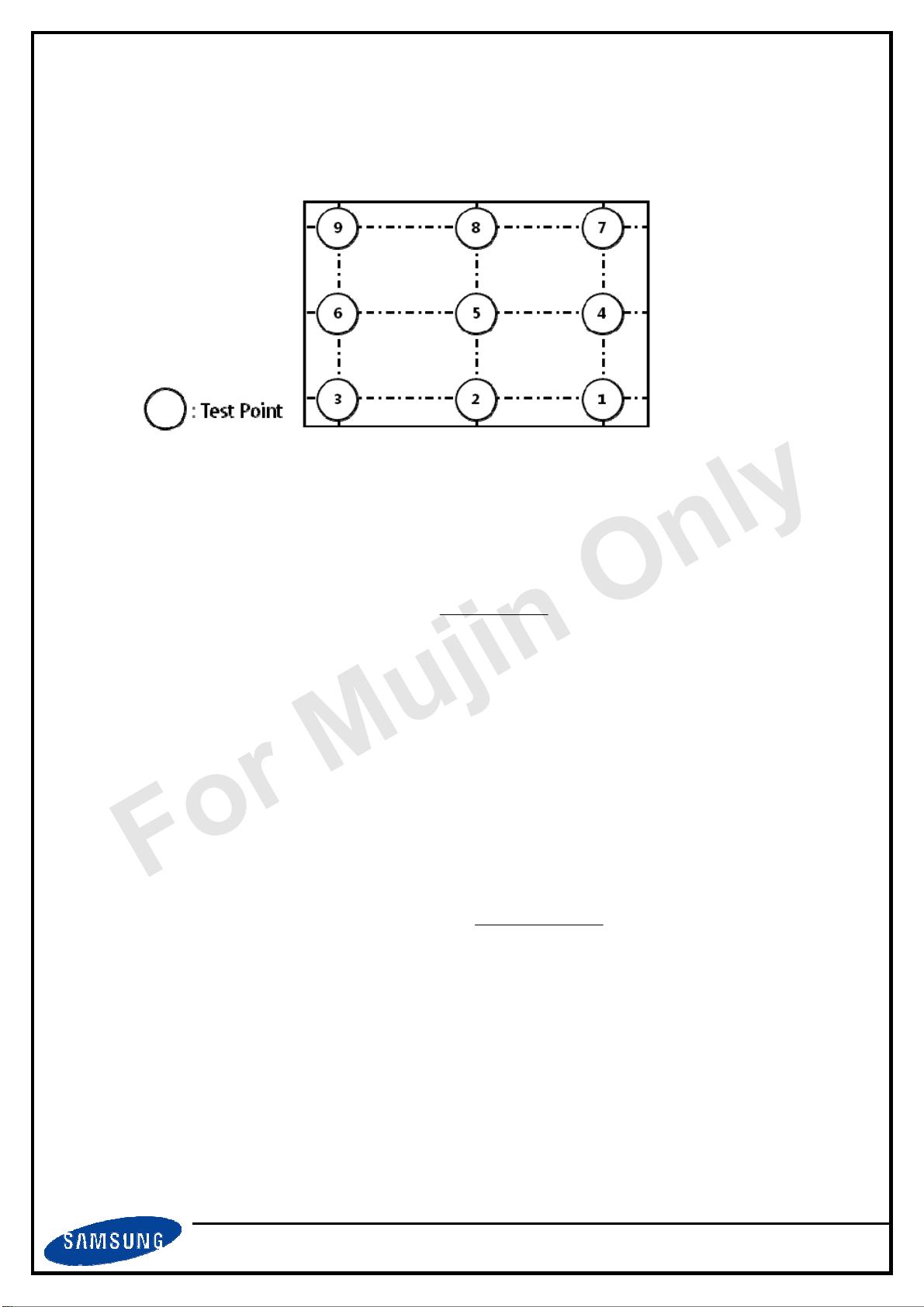
(2) Definition of test point
192
960
1728
Active Area
(3) Definition of Contrast Ratio (CR)
: Ratio of gray max (G
G
max
G
min
(4) Definition of 9 points brightness uniformity
) & gray min (G
max
G
CR =
G
: Luminance with all pixels white
: Luminance with all pixels black
B
B
= 100 x
uni
B
: Maximum brightness
max
B
: Minimum brightness
min
) at the center point⑤ of the panel
min
max
min
max
B
- B
max
min
108
540
972
35
P0.0
LTM270HL02
05. Jun. 2013
10
Page 11
/
SAMSUNG DISPLAY
For Mujin Only
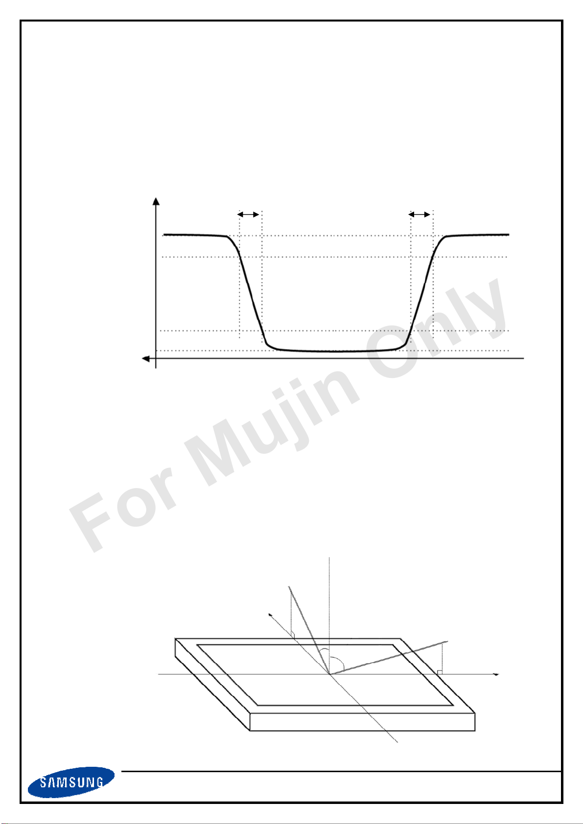
(5) Definition of Response time
GtoG : The time for transitions between specific gray levels
- 31 63, 63 95, 95 127, 127 159, 159 191 , 191 223 grays and vice
versa
- G to G typ. : Average time at rising and falling for gray transition except the
transition
Optical Instruments
Response
100 %
90 %
T
r
T
f
10 %
(6) Definition of Luminance of White : Luminance of white at center point (5)
(7) Definition of Color Chromaticity (CIE 1931, CIE1976)
Color coordinate of Red, Green, Blue & White at center point (5)
(8) Definition of Viewing Angle
: Viewing angle range (CR ≥ 10)
Normal
Ɵ
= ƟD= ƟL= ƟR = 0°
U
Y
ƟU = 90°0
Ɵ
U
Ɵ
R
Ɵ
= 90°0
R
X
11
35
Ɵ
L
= 90°0
P0.0
LTM270HL02
Ɵ
= 90°0
D
05. Jun. 2013
Page 12

/
For Mujin Only
4. Block Diagram
SAMSUNG DISPLAY
S1 S1920
(1920 x RGB x 1080 pixels)
Fig. Function Block Diagram
Note (1) The connector for display data & timing signal should be connected
35
P0.0
LTM270HL02
05. Jun. 2013
12
Page 13

/
For Mujin Only
5. Electrical Characteristics
SAMSUNG DISPLAY
5.1 TFT LCD Module
The connector for display data & timing signal should be connected.
Item
Voltage of Power Supply
Power Dip Condition
(a) White
Current of
Power
Supply
Power Consumption
(b) Black -
(c) Mosaic -
(d) Dot
Ta=25 ± 2°C
Symbol
Min.
Typ.
Max.
V
DD
V
CC
T
d
I
DD
P
LCD
4.5
4.0
0
- 668 - mA
-
5.0
-
-
349
492
714
2.46
5.5
V
DD
20
- mA
- mA
- mA
-
Unit
V
V
msec
Watt
Note
(1)
(2)
(3),(4)
(4),(5)
Rush Current
Note (1) The ripple voltage should be controlled under 10% of VDD
(2) Definition of V
- The above conditions are for the glitch of the input voltage.
- For stable operation of an LCD Module power, please follow them.
V
DD
90%
80%
GND
Power Dip
DD
If V
(Typ.) x 80% ≤ VCC ≤ VDD(Typ.) x 90%,
DD
I
RUSH
4.5V ≤ VDD ≤ 5.5V
then 0<Td ≤20msec
-
T
d
-
V
CC
5.0
A
(6)
35
P0.0
LTM270HL02
05. Jun. 2013
13
Page 14

/
SAMSUNG DISPLAY
For Mujin Only
(3) fV=60Hz, f
(4) Power dissipation check pattern (LCD Module only)
a) White Pattern b) Black Pattern
c)Mosaic Pattern d) Dot Pattern
= 67.3Hz, VDD = 5.0V, DC Current.
DCLK
(5) The power consumption is specified whereas Mosaic pattern is displayed
at fV=60Hz, f
(6) Measurement Condition
Rush Current I
= 67.3MHz, VDD = 5.0V
DCLK
can be measured when T
RUSH
. is 470㎲
RUSH
35
P0.0
LTM270HL02
05. Jun. 2013
14
Page 15

/
For Mujin Only
5.2 Backlight Unit
The characteristics of LED bar Ta=25 ± 2°C.
Item
SAMSUNG DISPLAY
Symbol Min. Typ. Max.
Unit Note
P
IF
VP
BLU
- 375 (390) mA (1),(2)
- 40.0 (44.0) V (1)
- 15.00 - Watt (3)
= IF (Typ.) x VP (Typ.)
BLU
LED Forward Current
LED Array Voltage
Power Consumption
Operating Life Time Hr 40,000 - - Hour (4)
Note (1) The above specification is not for the converter output, but for the LED bar.
- The LED bar consists of 39 LED packages ; 3 parallel X 13 serial
- LED current is defined at 100% duty ratio of LED driver
(2) The LED Forward current for single LED channel is Typ.125mA
- The output current of converter in the system should be transmitted to the LED
bar constantly.
- It is recommended to control the returned signal respectively for even
distribution of current to each channel of LED bar
(3) The power consumption is specified at typical current 375mA with 100% duty ratio
- It does not include power loss of external LED driver circuit block
- Typical power consumption P
(4) Life time(Hr) is defined as the time when brightness of a LED package itself
becomes 50% or less than its original value at the condition of Ta=25 ± 2°C
and IF =375mA.
35
P0.0
LTM270HL02
05. Jun. 2013
15
Page 16

/
SAMSUNG DISPLAY
For Mujin Only
5.3 LVDS Characteristics
5.3.1. LVDS Input Characteristics Ta=25 ± 2°C
Item
Symbol
Min. Typ. Max. Unit
Note
Differential Input
Voltage for LVDS
receiver threshold
LVDS skew
Differential input
voltage
Input voltage
range(single ended)
Common mode
voltage
High
Low
t
SKEW
lVidl
V
in
-
-100
-300
100
0.7
-
-
-
-
-
+100
-
300
600
1.7
mV
mV
ps
mV
V
(1)
(2)
(3)
(3)
V
cm
1.0
1.2
1.4
V
(3)
Note (1) Differential receiver voltage definitions and propagation delay and transition time
test circuit
a. All input pulses have frequency = 10MHz, t
b. C
Input
V
= (VIA+ V
IC
includes all probe and fixture capacitance
L
R
IN+
V
V
IA
R
IN-
V
IB
) / 2
IB
= VIA-V
D
or tF =1ns
R
IB
C
L
R
out
35
P0.0
LTM270HL02
05. Jun. 2013
16
Page 17

/
SAMSUNG DISPLAY
For Mujin Only
(2) LVDS Receiver DC parameters are measured under static and steady conditions
which may not be reflective of its performance in the end application.
T
LVDS Clk
V
= 0V
DIFF
LVDS Data
RX +/-
t
SKEW
where t
T : 1 period time of LVDS clock
cf. (-/+) of 300psec means LVDS data goes before or after LVDS clock
(3) Definition of VID and V
V
DD
VCM=1.4V
: skew between LVDS clock & LVDS data,
SKEW
using single-end signals
CM
|VID| = 100mV
VCM=1.4V
V
= 0V
DIFF
Differential
Differential
|VID| = 600mV
VCM=1.2V
VCM=1.0
V
SS
VCMrange with Min |VID|
|VID| = 100mV
VCM=1.0
|VID| = 600mV
VCMrange with Max |VID|
35
P0.0
LTM270HL02
05. Jun. 2013
17
Page 18

/
For Mujin Only
5.3.2. LVDS Data Format
Timing Diagrams of LVDS For Transmitting
- LVDS Receiver : Integrated T-CON
SAMSUNG DISPLAY
35
P0.0
LTM270HL02
05. Jun. 2013
18
Page 19

/
SAMSUNG DISPLAY
For Mujin Only
5.4 Interface Timing Specification
5.4.1. Timing Parameters
SIGNAL ITEM SYMBOL Min. Typ. Max. Unit Note
Clock
Hsync
Vsync
Vertical
Display Term
Horizontal
Display Term
Frequency
Active
Display
Period
Vertical
Tot al
Active
Display
Period
Horizontal
Tot al
1/TC
FH
FV
TVD
TV
THD
TH
(56.0)
(54.2)
(1105) 1111 (1386) Lines
67.3
(92.5)
MHz
66.0
(83.8)
kHz
(49)
1080
960 960 960 Clocks
(990) 1010 (1040) clocks
60
1080
(75)
1080
Hz
Lines
2pixel/clock
-
-
-
-
-
2pixel/clock
Note (1) DE only mode
- While operation, DE signal should be have the same cycle.
(2) Best operation clock frequency is 67.3MHz(60Hz)
(3) Max, Min variation range is at main clock typical value 67.3MHz
(4) Main frequency Max is 92.5MHz without spread spectrum
35
P0.0
LTM270HL02
05. Jun. 2013
19
Page 20

/
For Mujin Only
5.4.2. Timing diagrams of interface signal ( DE only mode )
T
V
SAMSUNG DISPLAY
DE
DE
D
CLK
DATA
SIGNALS
T
VD
T
H
T
HD
T
VB
T
C
T
C
T
CH
D
CLK
T
DS
DISPLAY
DATA
T
ES
DE
T
CL
0.5 V
T
DH
0.5 V
0.5 V
CC
CC
CC
35
P0.0
LTM270HL02
05. Jun. 2013
20
Page 21

/
SAMSUNG DISPLAY
For Mujin Only
5.5 Input Signals, Basic Display Colors and Gray Scale of Each Color
COLOR
BASIC
COLOR
GRAY
SCALE
OF
RED
DATA SIGNAL
DISPLAY
(8bit)
R0 R1 R2 R3 R4 R5 R6 R7 G0 G1 G2 G3 G4 G5 G6 G7 B0 B1 B2 B3 B4 B5 B6 B7
BLACK 0 0 0 0 0 0 0 0 0 0 0 0 0 0 0 0 0 0 0 0 0 0 0 0 -
BLUE 0 0 0 0 0 0 0 0 0 0 0 0 0 0 0 0 1 1 1 1 1 1 1 1 -
GREEN 0 0 0 0 0 0 0 0 1 1 1 1 1 1 1 1 0 0 0 0 0 0 0 0 -
CYAN 0 0 0 0 0 0 0 0 1 1 1 1 1 1 1 1 1 1 1 1 1 1 1 1 -
RED 1 1 1 1 1 1 1 1 0 0 0 0 0 0 0 0 0 0 0 0 0 0 0 0 -
MAGENTA 1 1 1 1 1 1 1 1 0 0 0 0 0 0 0 0 1 1 1 1 1 1 1 1 -
YELLOW 1 1 1 1 1 1 1 1 1 1 1 1 1 1 1 1 0 0 0 0 0 0 0 0 -
WHITE 1 1 1 1 1 1 1 1 1 1 1 1 1 1 1 1 1 1 1 1 1 1 1 1 BLACK 0 0 0 0 0 0 0 0 0 0 0 0 0 0 0 0 0 0 0 0 0 0 0 0 R0
1 0 0 0 0 0 0 0 0 0 0 0 0 0 0 0 0 0 0 0 0 0 0 0 R1
DARK
↑
↓
LIGHT
0 1 0 0 0 0 0 0 0 0 0 0 0 0 0 0 0 0 0 0 0 0 0 0 R2
: : : : : : : : : : : : : : : : : :
1 0 1 1 1 1 1 1 0 0 0 0 0 0 0 0 0 0 0 0 0 0 0 0 R253
RED GREEN BLUE
GRAY
SCALE
LEVEL
.
.
.
GRAY SCALE
OF GREEN
GRAY
SCALE
OF BLUE
0 1 1 1 1 1 1 1 0 0 0 0 0 0 0 0 0 0 0 0 0 0 0 0 R254
RED 1 1 1 1 1 1 1 1 0 0 0 0 0 0 0 0 0 0 0 0 0 0 0 0 R255
BLACK 0 0 0 0 0 0 0 0 0 0 0 0 0 0 0 0 0 0 0 0 0 0 0 0 G0
0 0 0 0 0 0 0 0 1 0 0 0 0 0 0 0 0 0 0 0 0 0 0 0 G1
DARK
↑
↓
LIGHT
GREEN 0 0 0 0 0 0 0 0 1 1 1 1 1 1 1 1 0 0 0 0 0 0 0 0 G255
BLACK 0 0 0 0 0 0 0 0 0 0 0 0 0 0 0 0 0 0 0 0 0 0 0 0 B0
DARK
↑
↓
LIGHT
BLUE 0 0 0 0 0 0 0 0 0 0 0 0 0 0 0 0 1 1 1 1 1 1 1 1 B255
0 0 0 0 0 0 0 0 0 1 0 0 0 0 0 0 0 0 0 0 0 0 0 0 G2
.
: : : : : : : : : : : : : : : : : :
0 0 0 0 0 0 0 0 1 0 1 1 1 1 1 1 0 0 0 0 0 0 0 0 G253
0 0 0 0 0 0 0 0 0 1 1 1 1 1 1 1 0 0 0 0 0 0 0 0 G254
0 0 0 0 0 0 0 0 0 0 0 0 0 0 0 0 1 0 0 0 0 0 0 0 B1
0 0 0 0 0 0 0 0 0 0 0 0 0 0 0 0 0 1 0 0 0 0 0 0 B2
: : : : : : : : : : : : : : : : : :
0 0 0 0 0 0 0 0 0 0 0 0 0 0 0 0 1 0 1 1 1 1 1 1 B253
0 0 0 0 0 0 0 0 0 0 0 0 0 0 0 0 0 1 1 1 1 1 1 1 B254
.
.
.
.
.
Note (1) Definition of Gray
- Rn : Red Gray, Gn : Green Gray, Bn : Blue Gray (n = Gray level)
Input Signal : 0 = Low level voltage, 1 = High level voltage
35
P0.0
LTM270HL02
05. Jun. 2013
21
Page 22

/
For Mujin Only
5.6 Power ON/OFF Sequence
To prevent a latch-up or DC operation of the LCD Module, the power on/off
sequence should be as the diagram below.
Power Supply (VDD)
0 V
0.1 V
DD
0.9 V
DD
T
1
T
2
SAMSUNG DISPLAY
0.9 V
DD
0.1 V
DD
T
3
T
4
Signals
Power On
T
5
SYMBOL Min. Typ. Max. Unit Description
T
1
T
2
T
3
T
4
T
5
0.5
0.01
0.01
1
500
-
10
ms
-
50
ms
-
50
ms
-
-
-
-
s
ms The time from valid data to B/L enable at power ON
VALID
Power Off
50% 50%
T
6
VDD rising time from 10% to 90%
The time from VDD to valid data at power ON
The time from valid data off to VDD off at power Off
VDD off time for Windows restart
T
6
Note (1) The supply voltage of the external system for the Module input should be
(3) In case of VDD = off level,
please keep the level of input signals low or keep a high impedance.
(4) T4 should be measured after the Module has been fully discharged between
power off and on period.
(5) Interface signal should not be kept at high impedance when the power is on.
100
-
the same as the definition of VDD.
(2) Apply the BLU power within the LCD operation range. When the back light
turns on before the LCD operation or the LCD turns off before the back light
turns off, the display may momentarily show abnormal screen.
P0.0
-
ms
The time from valid data off to B/L disable at power Off
LTM270HL02
05. Jun. 2013
22
35
Page 23

/
For Mujin Only
5.7 Input Terminal Pin Assignment
5.7.1. Input signal & Power Pin Assignment
Connector : P-TWO 187053-30091 or equivalent
SAMSUNG DISPLAY
Pin No.
1
2
3
4
5
6
7
8
9
10
11
12
13
Symbol
RXO0N
RXO0P
RXO1N
RXO1P
RXO2N
RXO2P
GND High speed ground
RXOC-
RXOC+
RXO3N
RXO3P
RXE0N
RXE0P
Negative LVDS differential data output
Positive LVDS differential data output
Negative LVDS differential data output
Positive LVDS differential data output
Negative LVDS differential data output
Positive LVDS differential data output
Negative Sampling Clock (ODD data)
Positive Sampling Clock (ODD data)
Negative LVDS differential data output
Positive LVDS differential data output
Negative LVDS differential data output
Positive LVDS differential data output
Function
14
15
16
17
18
19
20
21
22
23
24
25
26
27
GND High speed ground
RXE1N
RXE1P
GND High speed ground
RXE2N
RXE2P
RXEC-
RXEC+
RXE3N
RXE3P
GND LCD logic and driver ground
NC * Reserved for LCD manufacturer's use (CE_DVR)
NC * Reserved for LCD manufacturer's use (CTL_DVR)
NC No Connection
Negative LVDS differential data output
Positive LVDS differential data output
Negative LVDS differential data output
Positive LVDS differential data output
Negative Sampling Clock (EVEN data)
Positive Sampling Clock (EVEN data)
Negative LVDS differential data output
Positive LVDS differential data output
28
29
30
VDD
VDD
VDD
P0.0
Power Supply : +5V
LTM270HL02
35
05. Jun. 2013
23
Page 24

/
SAMSUNG DISPLAY
For Mujin Only
Note (1) If the system already uses the 25, 26pins, it should keep under GND level
The voltage applied to those pins should not exceed -200mV.
(2) Pin number starts from Left side
PCB
▼
▼
#1 #30
Pin No. 1 Pin No. 30
(3) All GND pins should be connected together and also be connected
to the LCD’s metal chassis.
(4) All power input pins should be connected together.
(5) All NC pins should be separated from other signal or power
UJU IS100-L30B-C23 or equivalent
P-TWO 187053-30091 or equivalent
#1 #30
Fig. Connector diagram
35
P0.0
LTM270HL02
05. Jun. 2013
24
Page 25

/
For Mujin Only
5.7.2. LED Connector Pin assignment
Connector : Molex 104086-0410 pr equivalent
- The mating type connector : Molex 104085-0410 or equivalent
SAMSUNG DISPLAY
Pin No.
Note (1) Pin number starts from Left side
1
2
3
4
Symbol
Vin LED power input
RTN 1 Channel 1 LED return
RTN 2 Channel 2 LED return
RTN 3 Channel 3 LED return
#1
Connector
Function
Rear view of panel
Fig. Connector diagram
#4 #1
▼
35
P0.0
LTM270HL02
05. Jun. 2013
25
Page 26

/
For Mujin Only
6. Outline Dimension
[ Refer to the next page ]
SAMSUNG DISPLAY
35
P0.0
LTM270HL02
05. Jun. 2013
26
Page 27

For Mujin Only
Page 28

/
For Mujin Only
7. Packing
7.1 Carton
SAMSUNG DISPLAY
Packing case
Pallet box
Item
Weight
Pallet
Packing form
-
8 panels in a case
8 cases in a box
64 panels in a box
-
Specification
- Total Weight ( Including Pallet ) : 260kg
- Packing Case Size : W281 x L692 x H412
- Material : Paper (SW,DW)
- Packing Pallet Box Size : W712 x L1144 x H794
- Material : Paper (SW,DW)
- Pallet Size : W800 x L1150 x H122
- Material : Wood
Packing Pallet
LTM270HL02 Module
( 8 EA )
Packing Case
Wood Pallet
35
P0.0
LTM270HL02
05. Jun. 2013
28
Page 29

/
SAMSUNG DISPLAY
For Mujin Only
7.2 Marking
A nameplate bearing followed by is affixed to a shipped product at the specified location
on each product.
(1) Parts number : LTM270HL02
(2) Revision: Three letters
(3) Lot number : X X X X XXX XX X
(4) Nameplate Indication
Cell Position No. (In the Glass)
Glass No. (In the one Lot)
Lot No. (Glass)
Month
Year
Product code
Line
(5) Packing box attach
LTM270HL02
35
P0.0
LTM270HL02
05. Jun. 2013
29
Page 30

/
SAMSUNG DISPLAY
For Mujin Only
8. General Precautions
8.1 Handling Precautions
A. When assembling LCD module into its system, using all the mounting holes is
strongly suggested.
B. Keep LCD module from any external shock or force which can cause physical damage
to LCD module. It may cause improper operation or damage to LCD module.
C. Polarizer films are very fragile. It could be damaged easily. Do not press or scratch
the surface harder than a HB pencil lead.
D. Wipe off water droplets or oil immediately. Water drops or oils can cause permanent
stain or discoloration.
E. To clean LCD module, please use IPA (Isopropyl Alcohol) or Hexane.
F. Do not use ketone type material (ex. Acetone), ethyl alcohol, toluene, ethyl acid or
methyl chloride. Using these could cause permanent polarizer damage to the LCD
module.
G. If the liquid crystal leaks from LCD module, keep it away from human eyes or mouth.
In case of contact with human body or clothes, it should be washed with soap thoroughly.
H. Protect LCD module from static discharge.
I. To keep the LCD module clean, make sure to wear fabric gloves and finger coats when
you are inspecting and/or assembling the unit.
J. Do not disassemble LCD module.
K. Protection film on LCD module display area should be slowly peeled off just before
assembly to prevent static discharge.
L. Pins of the Interface connector should not be touched directly with bare hands.
35
P0.0
LTM270HL02
05. Jun. 2013
30
Page 31

/
SAMSUNG DISPLAY
For Mujin Only
8.2 Storage Precautions
It is highly recommended to comply with the criteria in the table below
Item
Storage
Temperature
Storage
Humidity
Storage life
Storage
Condition
- The storage room should provide good ventilation and temperature
Control
.
- Products should not be placed on the floor, but on the Pallet away
from a wall
.
- Prevent products from direct sunlight, moisture nor water;
Be cautious of a build up of condensation.
Unit
(℃)
(%rH)
Min. Max.
5
35
12 months
40
75
- Avoid other hazardous environment while storing goods.
- If products delivered or kept in conditions of over the storage period
of 3 months, the recommended temperature or humidity range,
it is recommended to leave them at a temperature of 20℃ and a
humidity of 50% for 24 hours.
35
P0.0
LTM270HL02
05. Jun. 2013
31
Page 32

/
SAMSUNG DISPLAY
For Mujin Only
8.3 Operating Precautions
A. If the module is used to other applications besides the recommendation on General
Description, please contact SAMSUNG for application engineering device in advance
B. Do not connect or disconnect the LCD module when it is set to the “Power On”
condition.
C. Input power should always follow ‘5.6 Power on/off sequence’
D. Polarizer films are very fragile. It could be damaged easily. Do not press or scratch the
Polarizer films
E. LCD module contains electrical circuits that operate in high frequencies. To minimize
electromagnetic interference, be sure to sufficiently ground and shield the LCD module and
system.
F. If LCD module containing system is out of SAMSUNG ’s operating condition,
SAMSUNG can not guarantee LCD module operating properly.
G. If the product will be used in extreme conditions such as high temperature, humidity,
display patterns, operation time, etc., it is strongly recommended to contact SAMSUNG for
application engineering device. Otherwise, the reliability and function
of the module may not be guaranteed. Extreme conditions are commonly found at
airports, transit stations, banks, stocks, markets, and controlling systems.
H. Ultra-violet ray filter is necessary for outdoor operation.
I. If the module keeps displaying the same pattern for a long period of time, the image
maybe burned in to the screen. To avoid image retention, it is recommended to use a
screen saver.
J. This module has its PCB’s circuitry on the rear side and should be handled carefully in
order to avoid stress.
K. Please contact SAMSUNG beforehand, if you plan to display the same pattern for a
long period of time.
L. Any foreign materials brought into an LCD module by external forced-airflow are not
guaranteed by SAMSUNG .
35
P0.0
LTM270HL02
05. Jun. 2013
32
Page 33

/
SAMSUNG DISPLAY
For Mujin Only
9.4 Design Guide for System
8.4 Design Guide for System
A. The LED driver should be designed in compliance with the specifications of LED bar strictly to
make the LED in LCD module perform as expected
B. It is recommended that you locate the rib on the front or rear cover not to be placed on the
spot where D-IC is located on the upper or left of LCD module.
C. It is recommended that assemble the bracket which has two sides with holes for assembly.
D. It is recommended that you design the bracket with the structure which covers the sides
of module when designing the bracket for customer.
E. It is recommended that you design the bracket not to be interfered with the SET at the area
where the PBA of module is located.
F. It is recommended that more than 0.3 mm is allowable as a gap between the metal case
and the rear of module.
G. It is recommended that structure to support the module shall be far away 10mm from the
edge of border.
35
P0.0
LTM270HL02
05. Jun. 2013
33
Page 34

/
SAMSUNG DISPLAY
For Mujin Only
H. It is recommended that metal case (or board) shall be affixed to the rear case at the spot
where is far away 10mm from the edge of border.
I. When applying the measures described below to reduce the level of EMI which occurs
between the metal cover and the rear of module.
J. If you use Finger, less than 0.3mm is allowable for overlap.
K. It is recommended that more than 0.3mm gap between the front case (or cover) and
the panel glass is allowable.
L. It is recommended that more than 0.05mm gap between the front case and the top chassis
is allowable.
35
P0.0
LTM270HL02
05. Jun. 2013
34
Page 35

/
SAMSUNG DISPLAY
For Mujin Only
M. It is recommended that insert the screws into user holes from the ones on the parts, which
the light comes out to ones in the corresponding parts.
N. It is recommended that design the metal frame and the top chassis to be in parallel with having
no gap after inserting the side screw.
35
P0.0
LTM270HL02
05. Jun. 2013
35
 Loading...