

Page 1
CUSTOMER
Lenovo
MODEL
LTM270DL07
PROGRAM
Aventador / A740
EXTENSION CODE
M01
CUSTOMER APPROVAL & FEEDBACK
ARPPROVED BY
2 / Aug. / ’13 Nicolas Lee
PREPARED BY
2 / Aug. / ’13 Kevin Park
Application Engineering Group
Samsung Display Co., Ltd.
For Lenovo Only
PRODUCT SPECIFICATION
(√ ) PRODUCT INFORMATION
( ) APPROVAL SPECIFICATION
This Product Information is subject to change after 3 months of issuing date
Page 2
LTM270DL07
2. Aug. 2013
2/32
SAMSUNG DISPLAY
Ver.M07
P0.0
For Lenovo Only
Contents
Revision History ----------------------------------------------------------------------------------- (3)
1. General Description -------------------------------------------------------------------------------- (4)
2. Absolute Maximum Ratings ----------------------------------------------------------------------- (5)
3. Optical Characteristics ----------------------------------------------------------------------------- (7)
4. Block Diagram ------------------------------------------------------------------------------------ (11)
5. Electrical Characteristics -------------------------------------------------------------------------- (12)
5.1 TFT LCD Module
5.2 Back Light Unit
5.3 LED Driver
5.4 LVDS Input Characteristics
5.5 Timing Parameters
5.6 Input Signals, Basic Display Colors and Gray Scale of Each Color
5.7 Power ON/OFF Sequence
5.8 Input Terminal Pin Assignment
6. Outline Dimension -------------------------------------------------------------------------------- (27)
7. Packing -------------------------------------------------------------------------------------------- (29)
8. General Precautions ------------------------------------------------------------------------------- (30)
8.1 Handling Precautions
8.2 Storage Precautions
8.3 Operation Precaution
8.4 Others
Page 3
LTM270DL07
2. Aug. 2013
3/32
SAMSUNG DISPLAY
Ver.M07
P0.0
Version
Date
Page
Description
P0.0
2. Aug., 2013
All
Product information
For Lenovo Only
Revision History
Page 4
LTM270DL07
2. Aug. 2013
4/32
SAMSUNG DISPLAY
Ver.M07
P0.0
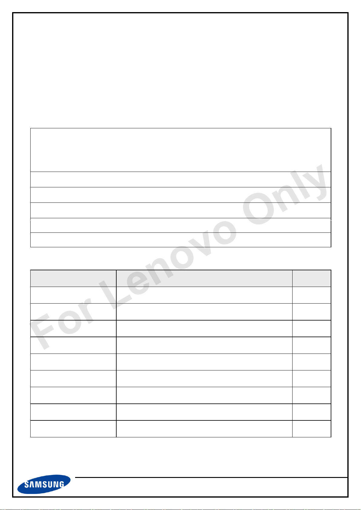
Application
- Workstation & Desktop monitors
- Display terminals for AV Products
- Monitors for Industrial machine
DE (Data Enable) only mode
LVDS (Low Voltage Differential Signaling) interface (4pixel/clock)
RoHS, Halogen Free
LED back light with an embedded LED driver (2-side)
Onboard EDID chip
Items
Specification
Unit
Pixel Pitch
0.233(H) x 0.233(W)
mm
Active Display Area
596.74(H) x 335.66(V)
mm
Surface Treatment
Glare type, Haze 1%
-
Display Colors
16.7M (True 8bit)
colors
Number of Pixels
2,560 x 1,440
pixel
Pixel Arrangement
RGB vertical stripe
-
Display Mode
Normally Black (PLS mode)
-
Luminance of White
300 (Typ.)
cd/㎡
Power Consumption
Total 21.0W (Typ. TBD) ( Panel 5.0W / BLU 16.0W)
W
For Lenovo Only
1. General Description
Overview
LTM270DL07 is a color active matrix liquid crystal display (LCD) that uses amorphous silicon
TFT (Thin Film Transistor) as switching components. This model is composed of a TFT LCD panel,
a driver circuit and a back light unit. The resolution of a 27.0” is 2560 x 1440 (QHD) and this
model can display up to 16.7 million colors.
Features
General Information
Page 5
LTM270DL07
2. Aug. 2013
5/32
SAMSUNG DISPLAY
Ver.M07
P0.0
Item
Min.
Typ.
Max.
Unit
Note
Module
size
Horizontal (H)
-
626.3
-
mm
w/o flange
Vertical (V)
-
362.6
-
mm
with shield case
Depth (D)
-
5.4
-
mm
-
Weight
-
-
(TBD)
g
LCD module only
Item
Symbol
Min.
Max.
Unit
Note
Power Supply Voltage
V
DD
GND-0.5
5.5
V
(1)
Operating Temperature
T
OPR
0
50
℃
(2)
Storage temperature
T
STG
-20
60
℃
Glass surface temperature
(Operation)
T
SUF
0
65
℃
(3)
For Lenovo Only
Mechanical Information
Note (1) Mechanical tolerance is ± 0.5mm unless there is a special comment.
2. Absolute Maximum Ratings
If the condition exceeds maximum ratings, it can cause malfunction or unrecoverable damage
to the device.
Note (1) Ta= 25 ± 2 °C
Page 6
LTM270DL07
2. Aug. 2013
6/32
SAMSUNG DISPLAY
Ver.M07
P0.0
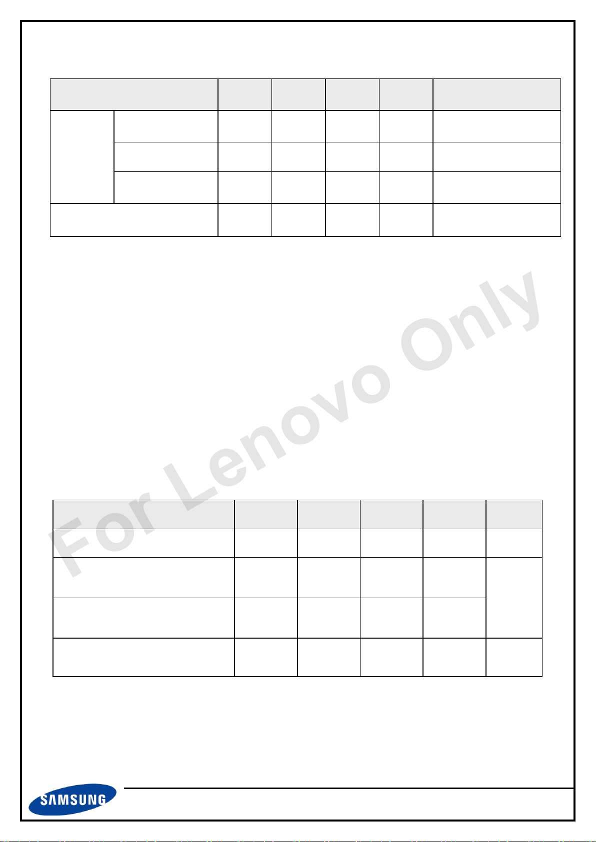
Fig. Temperature and Relative Humidity range
Operating Range
Storage Range
Relative Humidity (% RH)
(39, 90)
(50, 50.4)
(60, 27.7)
(-20, 10)
100
90
80
60
40
20
10
-40
-20
0
20
40
60
80
For Lenovo Only
(2) Temperature and relative humidity range are shown in the figure below.
a. 90 % RH Max. (Ta ≤ 39 °C)
b. Maximum wet-bulb temperature at 39 °C or less. (Ta ≤ 39 °C)
c. No condensation.
(3) The maximum operating temperature of LCD module is defined with surface
temperature of active area. Under any conditions, the maximum ambient operating
temperature should be keeping the surface of active area not higher than 65 °C
Page 7
LTM270DL07
2. Aug. 2013
7/32
SAMSUNG DISPLAY
Ver.M07
P0.0
Item
Symbol
Condition
Min.
Typ.
Max.
Unit
Note
Contrast Ratio
(Center of screen)
C/R
600
1000
-
(3)
SR-3
Response Time
G to G
Normal
θ
L,R
=0
θ
U,D
=0
Viewing
Angle
-
15
(25)
msec
(5)
RD-80S
Luminance of White
(Center of screen)
Y
L
(250)
300
-
cd/m
2
(6)
SR-3
Brightness Uniformity
(9 Points)
B
uni
- - 25
%
(4)
SR-3
Color
Chromaticity
(CIE 1931)
Red
Rx
- 0.030
(0.647)
+0.030
(7),(8)
SR-3
Ry
(0.341)
Green
Gx
(0.328)
Gy
(0.610)
Blue
Bx
(0.148)
By
(0.068)
White
Wx
0.310
Wy
0.340
Color
Chromaticity
(CIE 1976)
Red
Ru'
-
(0.446)
- Rv'
-
(0.529)
-
Green
Gu'
-
(0.136)
- Gv'
-
(0.568)
-
Blue
Bu'
-
(0.168)
- Bv'
-
(0.174)
-
White
Wu'
-
0.192
- Wv'
-
0.474
-
For Lenovo Only
3. Optical Characteristics
The optical characteristics should be measured in a dark room or equivalent.
Measuring equipment : SR-3, RD-80S (TOPCON), EZ-Contrast (Eldim)
(Ta = 25 ± 2°C, VDD=5V, fv= 60Hz, f
=60.38MHz, ( If =384mA))
DCLK
Page 8
LTM270DL07
2. Aug. 2013
8/32
SAMSUNG DISPLAY
Ver.M07
P0.0
Item
Symbol
Condition
Min.
Typ.
Max.
Unit
Note
Color Gamut
- -
(72)
-
% Color Temperature
- -
(6500)
-
K
Viewing
Angle
Hor.
θ
L
CR≥10
80
89
-
Degrees
(8)
EZ-
Contrast
θ
R
80
89
-
Ver.
θ
U
80
89
-
θ
D
80
89
-
Photo
detector
LCD Panel
TFT - LCD
Module
The center of the
screen
SR-3 : 50㎝
RD-80S : 50㎝
Field
2°
For Lenovo Only
Note (1) Test Equipment Setup
The measurement should be executed in a stable, windless and dark room between
30min after lighting the back light at the given temperature for stabilization of the
back light. This should be measured in the center of the screen.
LED forward current : If = (384mA) Environment condition : Ta = 25 ± 2 °C
Page 9
LTM270DL07
2. Aug. 2013
9/32
SAMSUNG DISPLAY
Ver.M07
P0.0
256
1280
2304
Active Area
144
720
1296
B
max
- B
min
B
max
B
uni
= 100 x
G
max
G
min
CR =
For Lenovo Only
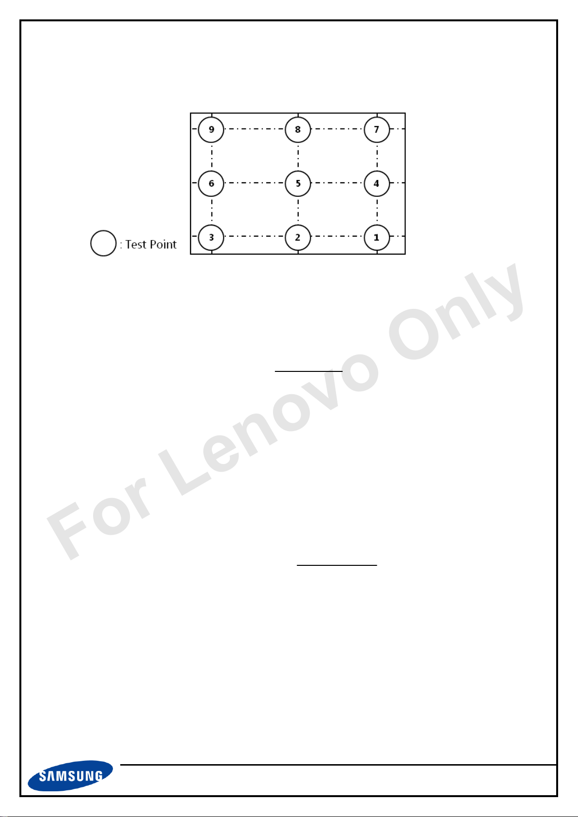
(2) Definition of test point
(3) Definition of Contrast Ratio (CR)
: Ratio of gray max (G
G
max
G
min
(4) Definition of 9 points brightness uniformity
) & gray min (G
max
: Luminance with all white pixels
: Luminance with all black pixels
B
: Maximum brightness
max
B
: Minimum brightness
min
) at the center point⑤ of the panel
min
Page 10
LTM270DL07
2. Aug. 2013
10/32
SAMSUNG DISPLAY
Ver.M07
P0.0
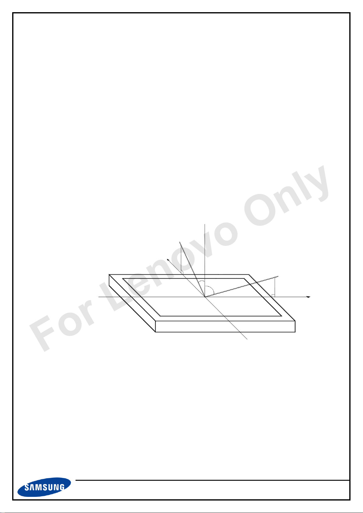
Y
X
Normal
ƟU = ƟD= ƟL= ƟR = 0°
Ɵ
U
Ɵ
R
ƟU = 90°0
ƟR = 90°0
ƟD = 90°0
ƟL = 90°0
For Lenovo Only
(5) Definition of Response time
GtoG : The time of transitions between specific gray levels
- 31 63, 63 95, 95 127, 127 159, 159 191 , 191 223 grays and vice
versa
- G to G typ. : Average time of rising and falling for gray transition except the
transition
(6) Definition of Luminance of White : Luminance of white at center point ⑤
(7) Definition of Color Chromaticity (CIE 1931, CIE1976)
Color coordinate of Red, Green, Blue & White at center point ⑤
(8) Definition of Viewing Angle
: Viewing angle range (CR ≥ 10)
Page 11

LTM270DL07
2. Aug. 2013
11/32
SAMSUNG DISPLAY
Ver.M07
P0.0
For Lenovo Only
4. Block Diagram
Page 12

LTM270DL07
2. Aug. 2013
12/32
SAMSUNG DISPLAY
Ver.M07
P0.0
Item
Symbol
Min.
Typ.
Max.
Unit
Note
Voltage of Power Supply
V
DD
4.5
5.0
5.5 V (1)
Power Dip Condition
V
CC
4.0
-
V
DD
V
(2)
T
d
0 - 20
msec
Current of
Power
Supply
(a) White
I
DD
-
(1000)
-
mA
(3),(4)
(b) Black
-
(TBD)
-
mA
(c) Dot
-
(TBD)
-
mA
Power Consumption
P
LCD
-
(5.0)
-
Watt
(4),(5)
Rush Current
I
RUSH
- - 5.0 A (6)
T
d
V
CC
V
DD
GND
90%
80%
4.5V ≤ VDD ≤ 5.5V
If VDD(Typ.) x 80% ≤ VCC ≤ VDD(Typ.) x 90%,
then 0<Td ≤20msec
For Lenovo Only
5. Electrical Characteristics
5.1 TFT LCD Module
The connector of display data & timing signal should be connected.
Ta=25 ± 2°C
Note (1) The ripple voltage should be controlled under 10% of VDD
(2) Definition of V
- The above conditions are for the glitch of the input voltage.
- For stable operation of an LCD Module power, please follow them.
Power Dip
DD
Page 13

LTM270DL07
2. Aug. 2013
13/32
SAMSUNG DISPLAY
Ver.M07
P0.0
a) White Pattern b) Black Pattern
c) Dot Pattern
For Lenovo Only
(3) fV=60Hz, f
(4) Power dissipation check pattern (LCD Module only)
= 60.38MHz, VDD = 5.0V, DC Current.
DCLK
(5) The power consumption is specified whereas Dot pattern is displayed
at fV=60Hz, f
(6) Measurement Condition
= 60.38MHz, VDD = 5.0V
DCLK
Rush Current I
can be measured when T
RUSH
. is 470㎲
RUSH
Page 14

LTM270DL07
2. Aug. 2013
14/32
SAMSUNG DISPLAY
Ver.M07
P0.0
Item
Symbol
Min.
Typ.
Max.
Unit
Note
LED Forward Current
I
F
-
(384)
-
mA
(1),(2)
LED Array Voltage
V
P
-
(40.6)
-
V
(1)
Power Consumption
P
BLU
(15.6)
Watt
(3)
Operating Life Time
Hr
(15,000)
-
-
Hour
(4)
For Lenovo Only
5.2 Backlight Unit
The characteristics of LED bar Ta=25 ± 2°C
Note (1) The specification shown above are not for the converter output, but for the LED bar.
- The LED bar consists of 224 LED packages ; 16 parallel X 14 serial
- LED current is defined at 100% duty ratio of LED driver
(2) The LED Forward current for single LED channel is Typ. (24mA)
- The output current of converter in the system should be transmitted to the LED
bar constantly.
- It is recommended to control the returned signal respectively for even
distribution of current to each channel of LED bar
(3) The power consumption is specified at typical current TBD with 100% duty ratio
- It does not include power loss of external LED driver circuit block
- Typical power consumption P
(4) Life time(Hr) is defined as the time when brightness of a LED package itself
becomes 50% or less than its original value at the condition of Ta=25 ± 2°C
and IF =(384mA.)
= IF (Typ.) x VP (Typ.)
BLU
Page 15

LTM270DL07
2. Aug. 2013
15/32
SAMSUNG DISPLAY
Ver.M07
P0.0
Item
Symbol
Min.
Typ.
Max.
Unit
Note
Input Voltage
V
BL_PWR
(TBD)
12
(TBD)
V
Input Current
I
BL_PWR
-
(TBD)
(TBD)
mA
Vin=12V Duty 100%
PWM duty Ratio
D
BL_PWM_DIM
1
-
(TBD)
%
PWM : 200Hz~1kHz
PWM : 1kHz~10kHz
PWM : 10kHz~20kHz
*PWMI min duty 1% @
DPST_EN*
(TBD)
(TBD)
(TBD)
(TBD)
External PWM
Frequency
F
BL_PWM_DIM
(TBD)
(TBD)
(TBD)
kHz
In-Rush Current
I
RUSH_BL_PWR
-
-
(TBD)
A
(1)
For Lenovo Only
5.3 LED Driver
The manufacturer of LED driver : (Richtek RT8561) Ta= 25 2 C
Note (1) Rush current measurement condition
Page 16

LTM270DL07
2. Aug. 2013
16/32
SAMSUNG DISPLAY
Ver.M07
P0.0
R
out
C
L
Input
R
IN+
R
IN-
V
D
= VIA- V
IB
V
IB
V
IA
V
IC
= (VIA+ V
IB
) / 2
Item
Symbol
Min.
Typ.
Max.
Unit
Note
Differential Input
Voltage for LVDS
receiver threshold
High
- - +100
mV
(1)
Low
-100 - - mV LVDS skew
t
SKEW
-300 - 300 ps
(2)
Differential input
voltage
lVidl
100
- 600
mV
(3)
Input voltage
range(single ended)
V
in
0.7 - 1.7 V
(3)
Common mode
voltage
V
cm
1.0 1.2 1.4 V
(3)
For Lenovo Only
5.4 LVDS Characteristics
5.4.1. LVDS Input Characteristics Ta=25 ± 2°C
Note (1) Differential receiver voltage definitions and propagation delay and transition time
test circuit
a. All input pulses have frequency of 10MHz, tR or tF =1ns
b. CL includes all probe and fixture capacitance
Page 17

LTM270DL07
2. Aug. 2013
17/32
SAMSUNG DISPLAY
Ver.M07
P0.0
Differential
LVDS Data
RX +/-
t
SKEW
T
V
DIFF
= 0V
V
DIFF
= 0V
Differential
LVDS Clk
VCM=1.4V
VCM=1.2V
VCM=1.0
VCMrange with Min |VID|
VCMrange with Max |VID|
V
SS
V
DD
|VID| = 100mV
|VID| = 100mV
VCM=1.4V
VCM=1.0
|VID| = 600mV
|VID| = 600mV
For Lenovo Only
(2) LVDS Receiver DC parameters are measured under static and steady conditions
which may not be reflective of its performance in the end application.
where t
T : 1 period time of LVDS clock
cf. (-/+) of 300psec means LVDS data goes before or after LVDS clock
(3) Definition of VID and V
: skew between LVDS clock & LVDS data,
SKEW
using single-end signals
CM
Page 18

LTM270DL07
2. Aug. 2013
18/32
SAMSUNG DISPLAY
Ver.M07
P0.0
For Lenovo Only
5.4.2. LVDS Data Format
Timing Diagrams of LVDS For Transmitting
- LVDS Receiver : Integrated T-CON
Page 19

LTM270DL07
2. Aug. 2013
19/32
SAMSUNG DISPLAY
Ver.M07
P0.0
SIGNAL
ITEM
SYMBOL
Min.
Typ.
Max.
Unit
Note
Clock
Frequency
1/TC
55.25
60.38
65.63
MHz
-
Hsync
FH
81.25
88.79
96.51
kHz
-
Vsync
FV
55
60
65
Hz
-
Vertical
Display Term
Active
Display
Period
TVD
1440
1440
1440
Lines
-
Vertical
Total
TV
1478
1481
1485
Lines
-
Horizontal
Display Term
Active
Display
Period
THD
640
640
640
Clocks
4pixel/clock
Horizontal
Total
TH
680
680
680
clocks
4pixel/clock
For Lenovo Only
5.5 Interface Timing Specification
5.5.1. Timing Parameters
Note (1) DE only mode
- While operation, DE signal should be have the same cycle.
(2) Best operation clock frequency is 60.38MHz(60Hz)
(3) Max, Min variation range is at main clock typical value (60.38MHz)
(4) Main frequency Max is 65.63MHz without spread spectrum
Page 20

LTM270DL07
2. Aug. 2013
20/32
SAMSUNG DISPLAY
Ver.M07
P0.0
DATA
SIGNALS
DE
D
CLK
DE
0.5 V
CC
T
C
DE
DISPLAY
DATA
0.5 V
CC
0.5 V
CC
T
CH
T
CL
T
DS
T
DH
T
ES
T
H
T
HD
T
V
T
VD
T
VB
T
C
D
CLK
For Lenovo Only
5.5.2. Timing diagrams of interface signal ( DE only mode )
Page 21

LTM270DL07
2. Aug. 2013
21/32
SAMSUNG DISPLAY
Ver.M07
P0.0
COLOR
DISPLAY
(8bit)
DATA SIGNAL
GRAY
SCALE
LEVEL
RED
GREEN
BLUE
R0
R1
R2
R3
R4
R5
R6
R7
G0
G1
G2
G3
G4
G5
G6
G7
B0
B1
B2
B3
B4
B5
B6
B7
BASIC
COLOR
BLACK
0 0 0 0 0 0 0 0 0 0 0 0 0 0 0 0 0 0 0 0 0 0 0 0 -
BLUE
0 0 0 0 0 0 0 0 0 0 0 0 0 0 0 0 1 1 1 1 1 1 1 1 -
GREEN
0 0 0 0 0 0 0 0 1 1 1 1 1 1 1 1 0 0 0 0 0 0 0 0 -
CYAN
0 0 0 0 0 0 0 0 1 1 1 1 1 1 1 1 1 1 1 1 1 1 1 1 -
RED
1 1 1 1 1 1 1 1 0 0 0 0 0 0 0 0 0 0 0 0 0 0 0 0 -
MAGENTA
1 1 1 1 1 1 1 1 0 0 0 0 0 0 0 0 1 1 1 1 1 1 1 1 -
YELLOW
1 1 1 1 1 1 1 1 1 1 1 1 1 1 1 1 0 0 0 0 0 0 0 0 -
WHITE
1 1 1 1 1 1 1 1 1 1 1 1 1 1 1 1 1 1 1 1 1 1 1 1 -
GRAY
SCALE
OF
RED
BLACK
0 0 0 0 0 0 0 0 0 0 0 0 0 0 0 0 0 0 0 0 0 0 0 0 R0
DARK
↑
↓
LIGHT
1 0 0 0 0 0 0 0 0 0 0 0 0 0 0 0 0 0 0 0 0 0 0 0 R1 0 1 0 0 0 0 0 0 0 0 0 0 0 0 0 0 0 0 0 0 0 0 0 0
R2
: : : : : : : : : : : : : : : : : :
. .
.
1 0 1 1 1 1 1 1 0 0 0 0 0 0 0 0 0 0 0 0 0 0 0 0 R253
0 1 1 1 1 1 1 1 0 0 0 0 0 0 0 0 0 0 0 0 0 0 0 0 R254
RED
1 1 1 1 1 1 1 1 0 0 0 0 0 0 0 0 0 0 0 0 0 0 0 0 R255
GRAY SCALE
OF GREEN
BLACK
0 0 0 0 0 0 0 0 0 0 0 0 0 0 0 0 0 0 0 0 0 0 0 0 G0
DARK
↑
↓
LIGHT
0 0 0 0 0 0 0 0 1 0 0 0 0 0 0 0 0 0 0 0 0 0 0 0 G1
0 0 0 0 0 0 0 0 0 1 0 0 0 0 0 0 0 0 0 0 0 0 0 0 G2
: : : : : : : : : : : : : : : : : :
. .
. 0 0 0 0 0 0 0 0 1 0 1 1 1 1 1 1 0 0 0 0 0 0 0 0
G253
0 0 0 0 0 0 0 0 0 1 1 1 1 1 1 1 0 0 0 0 0 0 0 0 G254
GREEN
0 0 0 0 0 0 0 0 1 1 1 1 1 1 1 1 0 0 0 0 0 0 0 0 G255
GRAY
SCALE
OF BLUE
BLACK
0 0 0 0 0 0 0 0 0 0 0 0 0 0 0 0 0 0 0 0 0 0 0 0 B0
DARK
↑
↓
LIGHT
0 0 0 0 0 0 0 0 0 0 0 0 0 0 0 0 1 0 0 0 0 0 0 0 B1 0 0 0 0 0 0 0 0 0 0 0 0 0 0 0 0 0 1 0 0 0 0 0 0
B2
: : : : : : : : : : : : : : : : : :
. .
. 0 0 0 0 0 0 0 0 0 0 0 0 0 0 0 0 1 0 1 1 1 1 1 1
B253
0 0 0 0 0 0 0 0 0 0 0 0 0 0 0 0 0 1 1 1 1 1 1 1 B254
BLUE
0 0 0 0 0 0 0 0 0 0 0 0 0 0 0 0 1 1 1 1 1 1 1 1 B255
For Lenovo Only
5.6 Input Signals, Basic Display Colors and Gray Scale of Each Color
Note (1) Definition of Gray
- Rn : Red Gray, Gn : Green Gray, Bn : Blue Gray (n = Gray level)
Input Signal : 0 = Low level voltage, 1 = High level voltage
Page 22

LTM270DL07
2. Aug. 2013
22/32
SAMSUNG DISPLAY
Ver.M07
P0.0
Timing (ms)
Remarks
0.5<T1≤10
VLCD_VCC rising time from 10% to 90%
0<T2 ≤50
Interval from VLCD_VCC to valid data at power ON
0<T3 ≤50
Interval from valid data OFF to VLCD_VCC OFF at power Off
500 ≤T4
VLCD_VCC OFF time for Windows restart
200 ≤T5
Interval from valid data to B/L enable at power ON
200 ≤T6
Interval from valid data off to B/L disable at power Off
0<T7 ≤10
VLCD_VCC falling time from 90% to 10%
10<T8
Interval from valid data on to LED driver Vin rising time 10%
10<T9
Interval from LED driver Vin falling time 10% to valid data Off
0.5<T10≤10
LED V
in
rising time from 10% to 90%
0.5<T11≤10
LED V
in
falling time from 90% to 10%
0<T12
Interval from LED driver Vin rising time 90% to PWM ON
0<T13
Interval from PWM Off to LED driver Vin falling time 90%
0 ≤ T14
Interval from PWM ON to B/L Enable ON
0 ≤ T15
Interval from B/L Enable Off to PWM Off
For Lenovo Only
5.7 Power ON/OFF Sequence
To prevent the product from being latched up or the DC in the LCD module from starting an
operation, the order to turn the power on and off should be changed to the order as shown in
the diagram below.
Page 23

LTM270DL07
2. Aug. 2013
23/32
SAMSUNG DISPLAY
Ver.M07
P0.0
For Lenovo Only
The backlight may be flashed if the interface signal remains floated when the above-mentioned
signal becomes invalid.
Note (1) The power voltage from system shall be supplied to the input pin of LCD constantly.
(2) Enable the voltage to the LED within the range, which the LCD is operated. The screen
becomes white when turning the back-light on before the LCD is operated or turning the
LCD off before turning the back-light off. Operation or the LCD turns off before the
back-light turns off, the display may momentarily become white.
(3) Don’t leave the system at a high impedance state, which the interface signal is out for
a long time after the Vcc is enabled.
(4) The T4 should be measured the module is fully discharged.
(5) The interface signal shall not maintain the high impedance when the power is on.
Page 24

LTM270DL07
2. Aug. 2013
24/32
SAMSUNG DISPLAY
Ver.M07
P0.0
PIN NO
SYMBOL
FUNCTION
1
1_RXO0N
1_Negative Transmission Data of Pixel 0
2
1_RXO0P
1_Positive Transmission Data of Pixel 0
3
1_RXO1N
1_Negative Transmission Data of Pixel 1
4
1_RXO1P
1_Positive Transmission Data of Pixel 1
5
1_RXO2N
1_Negative Transmission Data of Pixel 2
6
1_RXO2P
1_Positive Transmission Data of Pixel 2
7
GND
Power Ground
8
1_RXOC-
1_Negative Sampling Clock
9
1_RXOC+
1_Positive Sampling Clock
10
1_RXO3N
1_Negative Transmission Data of Pixel 3
11
1_RXO3P
1_Positive Transmission Data of Pixel 3
12
GND
Power Ground
13
2_RXO0N
2_Negative Transmission Data of Pixel 0
14
2_RXO0P
2_Positive Transmission Data of Pixel 0
15
2_RXO1N
2_Negative Transmission Data of Pixel 1
16
2_RXO1P
2_Positive Transmission Data of Pixel 1
17
2_RXO2N
2_Negative Transmission Data of Pixel 2
18
2_RXO2P
2_Positive Transmission Data of Pixel 2
19
GND
Power Ground
20
2_RXOC-
2_Negative Sampling Clock
21
2_RXOC+
2_Positive Sampling Clock
22
2_RXO3N
2_Negative Transmission Data of Pixel 3
23
2_RXO3P
2_Positive Transmission Data of Pixel 3
24
GND
Power Ground
25
GND
Power Ground
26
GND (BIST)
L(GND) = Black, H(3.3V) = Built – in – patterns toggle
27
NC
No Connection
28
VDD
Power Supply : +5V
29
VDD
Power Supply : +5V
30
VDD
Power Supply : +5V
For Lenovo Only
5.8 Input Terminal Pin Assignment
5.8.1. Input signal & Power Pin Assignment
Connector : 20455-030E-0 (DAICHI SEIKO) or the equipment with the equivalent capability
Page 25

LTM270DL07
2. Aug. 2013
25/32
SAMSUNG DISPLAY
Ver.M07
P0.0
PIN NO
SYMBOL
FUNCTION
1
3_RXO0N
3_Negative Transmission Data of Pixel 0
2
3_RXO0P
3_Positive Transmission Data of Pixel 0
3
3_RXO1N
3_Negative Transmission Data of Pixel 1
4
3_RXO1P
3_Positive Transmission Data of Pixel 1
5
3_RXO2N
3_Negative Transmission Data of Pixel 2
6
3_RXO2P
3_Positive Transmission Data of Pixel 2
7
GND
Power Ground
8
3_RXOC-
3_Negative Sampling Clock
9
3_RXOC+
3_Positive Sampling Clock
10
3_RXO3N
3_Negative Transmission Data of Pixel 3
11
3_RXO3P
3_Positive Transmission Data of Pixel 3
12
GND
Power Ground
13
4_RXO0N
4_Negative Transmission Data of Pixel 0
14
4_RXO0P
4_Positive Transmission Data of Pixel 0
15
4_RXO1N
4_Negative Transmission Data of Pixel 1
16
4_RXO1P
4_Positive Transmission Data of Pixel 1
17
4_RXO2N
4_Negative Transmission Data of Pixel 2
18
4_RXO2P
4_Positive Transmission Data of Pixel 2
19
GND
Power Ground
20
4_RXOC-
4_Negative Sampling Clock
21
4_RXOC+
4_Positive Sampling Clock
22
4_RXO3N
4_Negative Transmission Data of Pixel 3
23
4_RXO3P
4_Positive Transmission Data of Pixel 3
24
GND
Power Ground
25
NC(WP)
No connection
26
SCL
DDC Clock
27
SDA
DDC Data
28
GND
Power Ground
29~40
Please refer to the next page
For Lenovo Only
Connector : SD-104062-001-S01 (MOLEX) or the equipment with the equivalent capability
Page 26

LTM270DL07
2. Aug. 2013
26/32
SAMSUNG DISPLAY
Ver.M07
P0.0
PIN NO
SYMBOL
FUNCTION
29
PWM
PWM for luminance control
30
BL_EN
BL On/Off
31
VEDID 3.3V
DDC 3.3V Power for EDID
32
GND
Power Ground
33
NC
No connection
34
VBL_12V
LED Power Supply : +12V
35
VBL_12V
LED Power Supply : +12V
36
VBL_12V
LED Power Supply : +12V
37
VBL_12V
LED Power Supply : +12V
38
VBL_12V
LED Power Supply : +12V
39
VBL_12V
LED Power Supply : +12V
40
VBL_12V
LED Power Supply : +12V
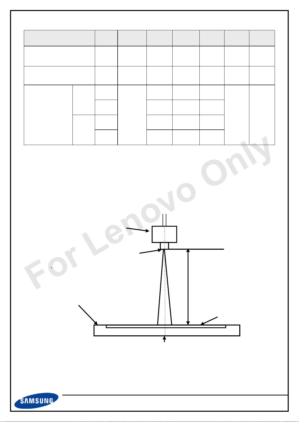
Fig. Connector diagram
Connector Inserting Direction
For Lenovo Only
Note (1) Pin number starts from the right
(2) All GND pins should be connected to each other and be connected
to the LCD’s metal chassis.
(3) All power input pins should be connected to each other.
(4) All NC pins should be separated from other signal or power
Page 27

LTM270DL07
2. Aug. 2013
27/32
SAMSUNG DISPLAY
Ver.M07
P0.0
For Lenovo Only
6. Outline Dimension
[ Refer to the next page ]
Page 28

Page 29

LTM270DL07
2. Aug. 2013
29/32
SAMSUNG DISPLAY
Ver.M07
P0.0
Cell Position No. (In the Glass)
Glass No. (In the one Lot)
Lot No. (Glass)
Month
Year
Product code
Line
LTM270DL07
For Lenovo Only
7. Packing
7.1 Marking
A nameplate bearing followed by is affixed to a shipped product at the specified location
on each product.
(1) Parts number : LTM270DL07
(2) Revision: Three letters
(3) Lot number : X X X X XXX XX X
(4) Nameplate Indication
(5) Packing box attach
Page 30

LTM270DL07
2. Aug. 2013
30/32
SAMSUNG DISPLAY
Ver.M07
P0.0
For Lenovo Only
8. General Precautions
8.1 Handling Precautions
A. When the module is assembled, It should be attached to the system firmly using every
mounting holes. Be careful not to twist and bend the modules.
B. Refrain from strong mechanical shock and / or any force to the module. In addition to
damage, this may cause improper operation or damage to the module and LED back-light.
C. Note that polarizers are very fragile and could be easily damaged. Do not press or scratch
the surface harder than a HB pencil lead.
D. Wipe off water droplets or oil immediately. If you leave the droplets for a long time,
Staining and discoloration may occur.
E. If the surface of the polarizer is dirty, clean it using some absorbent cotton or soft cloth.
F. The desirable cleaners are water, IPA (Isoprophyl Alcohol) or Hexane. Do not use Ketone
type materials(ex. Acetone), Ethyl alcohol, Toluene, Ethyl acid or Methyl chloride. It might
permanent damage to the polarizer due to chemical reaction.
G. If the liquid crystal material leaks from the panel, it should be kept away from the eyes or
mouth. In case of contact with hands, legs or clothes, it must be washed away thoroughly
with soap
H. Protect the module from static, it may cause damage to the C-MOS Gate Array IC.
I. Use fingerstalls with soft gloves in order to keep display clean during the incoming
inspection and assembly process.
J. Do not disassemble the module.
K. Do not pull or fold the LED FPC.
L. Do not touch any component which is located on the back side.
M. Protection film for polarizer on the module shall be slowly peeled off just before use so that
the electrostatic charge can be minimized.
N. Pins of I/F connector shall not be touched directly with bare hands.
Page 31

LTM270DL07
2. Aug. 2013
31/32
SAMSUNG DISPLAY
Ver.M07
P0.0
Item
Unit
Min.
Max.
Storage
Temperature
(℃) 5 40
Storage
Humidity
(%rH)
35
75
Storage life
12 months
Storage
Condition
- The storage room should be equipped with a good ventilation facility,
which has a temperature controlling system.
- Products should be placed on the pallet, which is away from the wall not
on the floor.
- Prevent products from being exposed to the direct sunlight, moisture, and
water. ; Be cautious not to pile the products up.
- Avoid storing products in the environment, which other hazardous material
is placed.
- If products are delivered or kept in the storage facility more than 3 months,
we recommend you to leave products under the condition including a 20℃
temperature and a humidity of 50% for 24 hours.
- If you store semi-manufactured products for more than 3 months, bake the
products under the condition including the 50℃ temp. and the 10%
humidity for 24hrs after being used.
For Lenovo Only
8.2 Storage Precautions
It is highly recommended to comply with the criteria in the table below
Page 32

LTM270DL07
2. Aug. 2013
32/32
SAMSUNG DISPLAY
Ver.M07
P0.0
For Lenovo Only
8.3 Operating Precautions
A. Do not connect, disconnect the module in “Power On” condition.
B. Power supply should always be turned on/off by following 5.7 “ Power on/off sequence”.
C. Module has high frequency circuits. Sufficient suppression to the electromagnetic
interference shall be done by system manufacturers. Grounding and shielding methods
may be important to minimize the interference.
D. The FPC cable between the LED chips and its converter power supply shall be a minimized
length and be connected directly .The longer cable between the back-light and the
converter may cause lower luminance of light source (LED).
E. The standard limited warranty is only applicable when the module is used for general
Notebook applications. If used for purposes other than as specified, SEC is not to be held
reliable for the defective operations. It is strongly recommended to contact SEC to find out
fitness for a particular purpose.
8.4 Others
A. Ultra-violet ray filter is necessary for outdoor operation.
B. Avoid condensation of water. It may result in improper operation or disconnection of
electrode.
C. Do not exceed the absolute maximum rating value. ( the supply voltage variation, input
voltage variation, in part contents and environmental temperature, so on) Otherwise the
module may be damaged.
D. If the module displays the same pattern continuously for a long period of time, it can be the
situation when The image “sticks” to the screen.
E. This module has its circuitry PCB’s on the rear side and should be handled carefully in order
not to be stressed.
 Loading...