

Page 1
Global LCD Panel Exchange Center
kUGu
tvkls
ISSUED DATE : 2007-04-11
www.panelook.com
Product Information
Product Information
SAMSUNG TFT--
SAMSUNG TFT
SAMSUNG TFT-LCD PRODUCT INFORMATION
MODEL : LTM240CT03
MODEL : LTM240CT03
MODEL : LTM240CT03
LCD PRODUCT INFORMATION
LCD PRODUCT INFORMATION
Note : This is Product Information is subject to change after 3 months of issuing date.
Development Team 4, LCD Business
Samsung Electronics Co . , LTD.
One step solution for LCD / PDP / OLED panel application: Datasheet, inventory and accessory!
s{tY[Wj{WZ
XVZ[wwpTWWWTs{tY[Wj{WZ
www.panelook.com
Page 2
Global LCD Panel Exchange Center
kUGu
tvkls
General Description
www.panelook.com
Product Information
Product Information
Description
LTM240CT03 is a color active matrix liquid crystal display (LCD) that uses amorphous
silicon TFT (Thin Film Transistor) as switching components. This model is composed of
a TFT LCD panel, a driver circuit and a back light unit. The resolution of a 24.0” is 1920
x 1200 and this model can display up to 16.7 millions colors.
Features
High contrast ratio, high aperture structure, High Color Gamut
TN (Twisted Nematic) mode
Wide Viewing Angle
High speed response
Wide UXGA (1920 x 1200 pixels) resolution
Low power consumption
DE (Data Enable) only mode
LVDS (Low Voltage Differential Signaling) interface (2pixel/clock)
Direct B/L Unit Design
RoHS compliance
Pb Free compliance
Applications
Workstation & desktop monitors
Display terminals for AV application products
Monitors for industrial machine
* If the module is used to other applications besides the above, please contact SEC
in advance.
General Information
ARC GlareSurface Treatment
UnitSpecificationItems
mm0.270(H) x 0.270(W)Pixel Pitch
mm518.4(H) x 324.0(V)Active Display Area
colors16.7M (Hi-FRC)Display Colors
pixel1920 x 1200Number of Pixels
RGB vertical stripePixel Arrangement
Note
Normally WhiteDisplay Mode
cd/༇400(Typ.)Luminance of White
One step solution for LCD / PDP / OLED panel application: Datasheet, inventory and accessory!
s{tY[Wj{WZ
ZVZ[wwpTWWWTs{tY[Wj{WZ
www.panelook.com
Page 3
Global LCD Panel Exchange Center
kUGu
tvkls
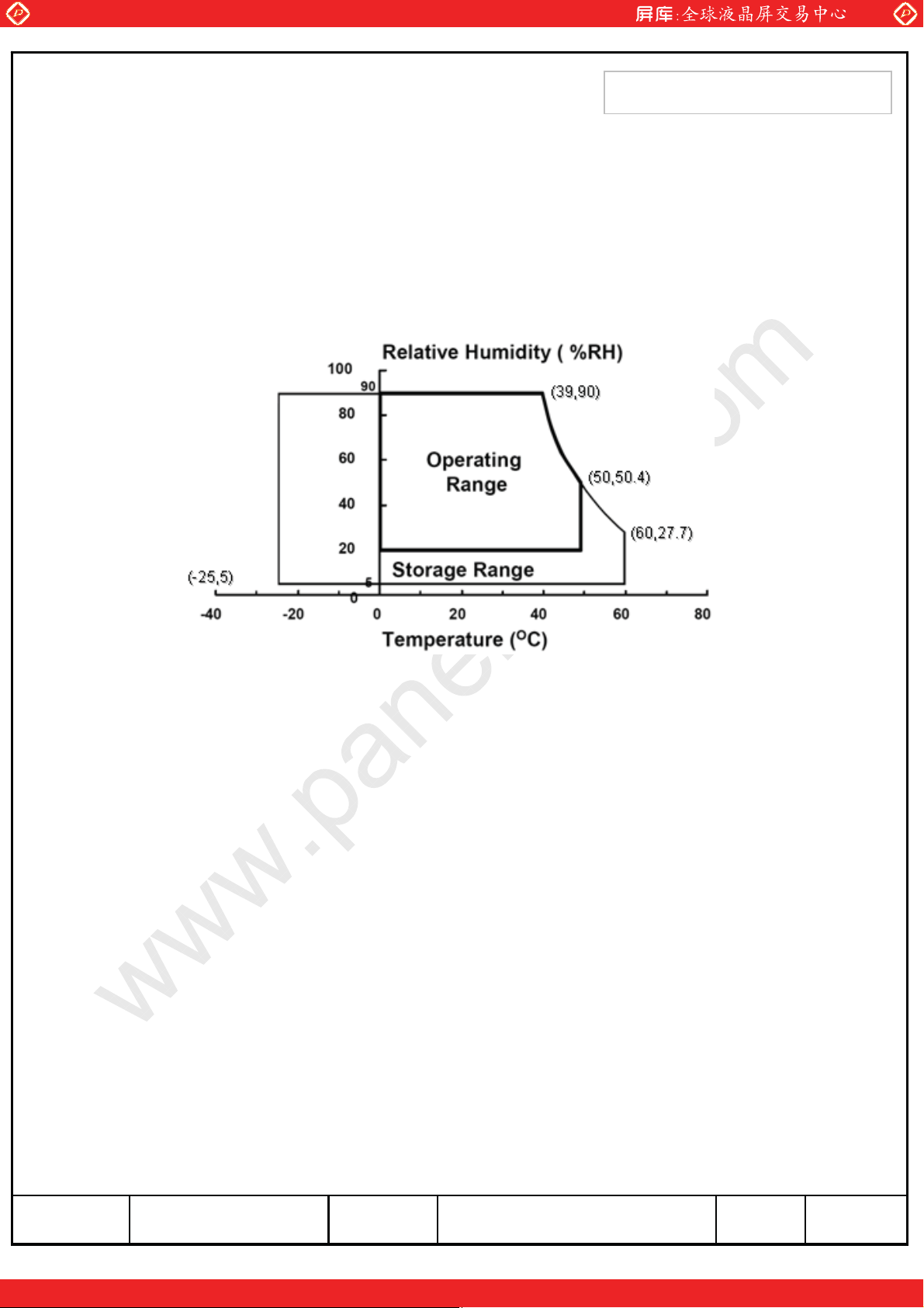
(1) Temperature and relative humidity range are shown in the figure below.
a. 90 % RH Max. (Ta ˺ 39 ¶C)
b. Maximum wet-bulb temperature at 39 ¶C or less. (Ta ˺ 39 ¶C)
c. No condensation
(2) 11ms, sine wave, one time for ·X, ·Y, ·Z axis
(3) 10-300 Hz, Sweep rate 10min, 30min for X,Y,Z axis
www.panelook.com
Product Information
Product Information
Fig. Temperature and Relative humidity range
One step solution for LCD / PDP / OLED panel application: Datasheet, inventory and accessory!
s{tY[Wj{WZ
\VZ[wwpTWWWTs{tY[Wj{WZ
www.panelook.com
Page 4
Global LCD Panel Exchange Center
kUGu
tvkls
www.panelook.com
Product Information
Product Information
NoteUnitMax.Typ.Min.ConditionSymbolItem
%-92--Color Gamut
K-6500--Color Temperature
ɂ
Hor.
Viewing
Angle
Ver.
Brightness Uniformity
(9 Points)
L
ɂ
R
ɂ
U
ɂ
D
uni
CR˻10
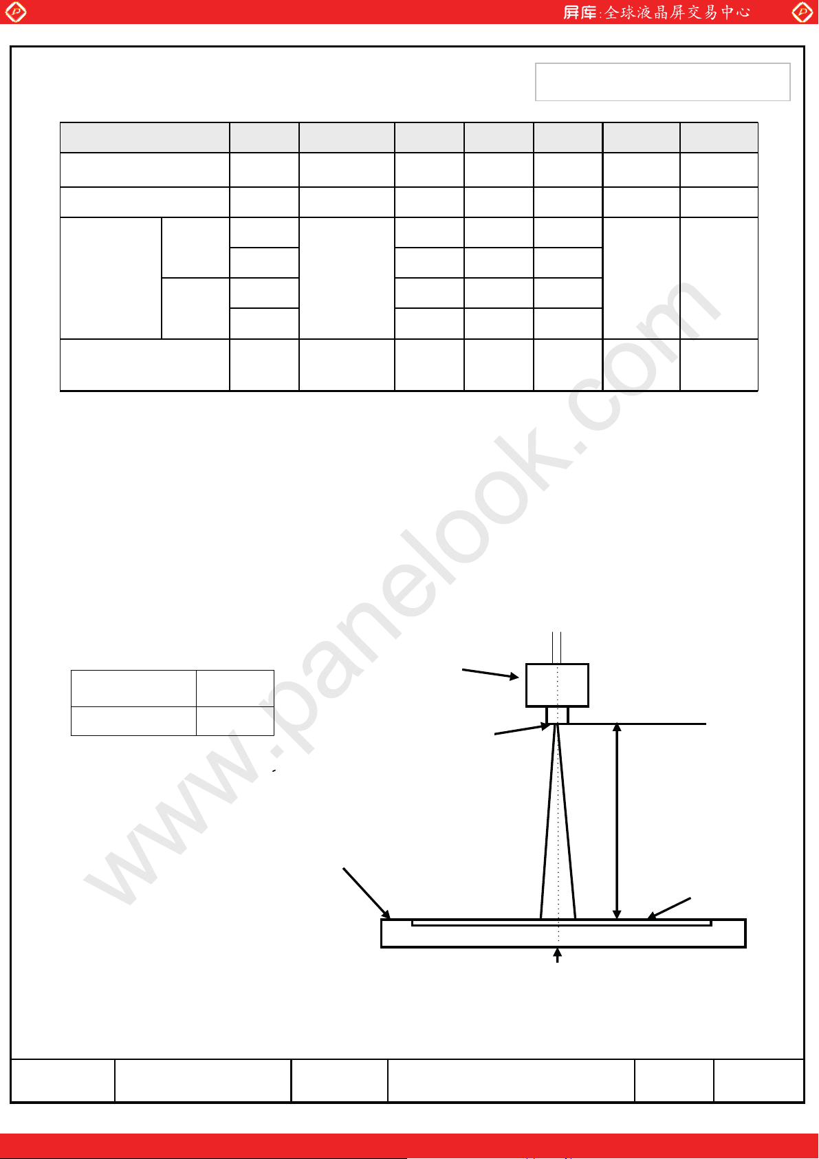
Note (1) Test Equipment Setup
The measurement should be executed in a stable, windless and dark room between
30min after lighting the back light at the given temperature for stabilization
of the back light. This should be measured in the center of screen.
Single lamp current : 6.0mA
Environment condition : Ta = 25 · 2 ¶C
-8070
-8070
Degrees
-8070
-8070
%25--B
(8)
EZ-
Contrast
(4)
SR-3
FieldPhoto detector
1°SR-3
TFT - LCD Module
Photo detector
Field
SR-3 : 40㎝
RD-80S : 50㎝
LCD Panel
The center of the screen
One step solution for LCD / PDP / OLED panel application: Datasheet, inventory and accessory!
s{tY[Wj{WZ
^VZ[wwpTWWWTs{tY[Wj{WZ
www.panelook.com
Page 5
Global LCD Panel Exchange Center
kUGu
tvkls
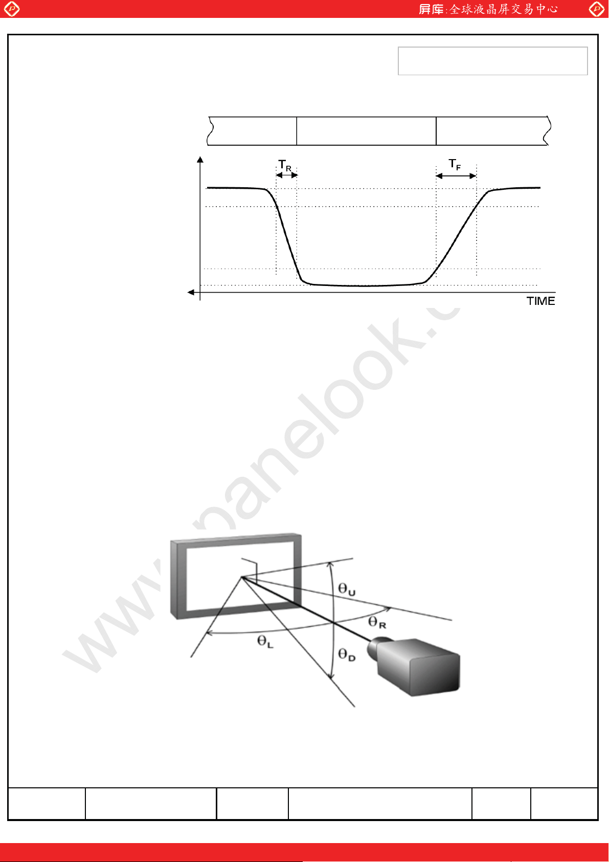
Note (5) Definition of Response time : Sum of Tr, Tf
Display Data White(TFT off) Black(TFT on) White(TFT off)
www.panelook.com
Product Information
Product Information
Optical Instruments
Response
Note (6) Definition of Luminance of White : Luminance of white at center point㽶
Note (7) Definition of Color Chromaticity (CIE 1931, CIE1976)
Color coordinate of Red, Green, Blue & White at center point㽶
100%
90%
10%
0%
Note (8) Definition of Viewing Angle
: Viewing angle range (CR ı10)
One step solution for LCD / PDP / OLED panel application: Datasheet, inventory and accessory!
s{tY[Wj{WZ
`VZ[wwpTWWWTs{tY[Wj{WZ
www.panelook.com
Page 6
Global LCD Panel Exchange Center
kUGu
tvkls
3. Electrical Characteristics
3.1 TFT LCD Module
The connector for display data & timing signal should be connected.
www.panelook.com
Product Information
Product Information
Ta = 25¶C
NoteUnitMax.Typ.Min.SymbolItem
Voltage of Power Supply
Differential Input
Voltage for LVDS
Receiver Threshold
LVDS skew
LVDS
Input
Differential input
voltage
Characteri
stics
Input voltage range
(single-ended)
Common mode
voltage
Input current
Current of
(a) Black
Power
Supply
DD
SKEW
IN
V
CM
IN
I
DD
0+
|VID|/2
1.2
2.4-
|V
±10I
(1)V5.55.04.5V
(2)mV+100--High
mV---100Low
(3)300-300t
(4)mV600200|VID|
(4)V2.40V
(4)V
|/2
ID
㎂
mA2,0001,700-
mA2,3002,000-(b) White (5),(6)
mA3,0002,400-(c) Dot
Vsync Frequency
Hsync Frequency
Main Frequency
Rush Current
V
H
DCLK
RUSH
Note (1) The ripple voltage should be controlled under 10% of VDD.
Hz636053f
kHz787465f
MHz817768f
(7)A5.0--I
One step solution for LCD / PDP / OLED panel application: Datasheet, inventory and accessory!
s{tY[Wj{WZ
XXVZ[wwpTWWWTs{tY[Wj{WZ
www.panelook.com
Page 7

Global LCD Panel Exchange Center
kUGu
tvkls
(5) fV=60Hz, fDCLK = 54MHz, VDD = 5.0V, DC Current.
(6) Power dissipation check pattern (LCD Module only)
a) White Pattern b) Black Pattern c) Dot Pattern
www.panelook.com
Product Information
Product Information
(7) Measurement Condition
100%
90%
10%
GND
Rush Current I
RUSH
T
=470༕
RUSH
can be measured when T
. is 470༕.
RUSH
V
DD
One step solution for LCD / PDP / OLED panel application: Datasheet, inventory and accessory!
s{tY[Wj{WZ
XZVZ[wwpTWWWTs{tY[Wj{WZ
www.panelook.com
Page 8

Global LCD Panel Exchange Center
kUGu
tvkls
(2) Lamp frequency which may produce interference with horizontal synchronous
frequency may cause line flow on the display. Therefore lamp frequency should be
detached from the horizontal synchronous frequency and its harmonics as far as
possible in order to avoid interference.
(3) Life time (Hr) is defined as the time when brightness of a lamp unit itself becomes
www.panelook.com
Product Information
Product Information
50% or less than its original value at the condition of Ta = 25·2¶C and I
(4) Designing a system inverter intended to have better display performance, power
efficiency and lamp reliability.
They would help increase the lamp lifetime and reduce leakage current.
a. The measurement should be done at typical lamp current.
b. The asymmetry rate of the inverter waveform should be less than 10%.
c. The distortion rate of the waveform should be √2 with ±10% tolerance.
- Inverter output waveform had better be more similar to ideal sine wave.
Asymmetry rate
p-p
||II
I
p
I
u 100
rms
= 6.0mArms
L
(5) If an inverter has shutdown function, it should keep its output for over 1 second
I
-p
Fig. Wave form of the inverter
even if the lamp connector is open. Otherwise the lamps may not be turned on.
s{tY[Wj{WZ
Distortion rate
p
I
||
rms
I
or
-p
I
||
rms
I
X\VZ[wwpTWWWTs{tY[Wj{WZ
One step solution for LCD / PDP / OLED panel application: Datasheet, inventory and accessory!
www.panelook.com
Page 9

Global LCD Panel Exchange Center
kUGu
tvkls
5. Input Terminal Pin Assignment
www.panelook.com
Product Information
Product Information
5.1. Input Signal & Power ( Connector : UJU, IS100-L30O-C23 or equivalent )
FUNCTIONSYMBOLPIN NO
1
2
3
4
5
6
7
8
9
10
11
12
13
14
15
RXO0P
RXO1N
Negative LVDS differential data outputRXO0N
Positive LVDS differential data output
Negative LVDS differential data output
Positive LVDS differential data outputRXO1P
Negative LVDS differential data outputRXO2N
Positive LVDS differential data outputRXO2P
GroundGND
Negative Sampling Clock (ODD data)RXOC-
Positive Sampling Clock (ODD data)RXOC+
Negative LVDS differential data outputRXO3N
Positive LVDS differential data outputRXO3P
Negative LVDS differential data outputRXE0N
Positive LVDS differential data outputRXE0P
GroundGND
Negative LVDS differential data outputRXE1N
16
17
18
19
20
21
22
23
24
25
26
27
28
29
30
Positive LVDS differential data outputRXE1P
GroundGND
Negative LVDS differential data outputRXE2N
Positive LVDS differential data outputRXE2P
Negative Sampling Clock (EVEN data)RXEC-
Positive Sampling Clock (EVEN data)RXEC+
Negative LVDS differential data outputRXE3N
Positive LVDS differential data outputRXE3P
GroundGND
* CE (For LCD internal use only. Do not connect)NC
* CTL (For LCD internal use only. Do not connect)NC
VDD
VDD
Power Supply : +5V
VDD
VDD
* If the system already uses the 25, 26pins, it should keep under GND level
The voltage applied to those pins should not exceed -200mV.
One step solution for LCD / PDP / OLED panel application: Datasheet, inventory and accessory!
s{tY[Wj{WZ
X^VZ[wwpTWWWTs{tY[Wj{WZ
www.panelook.com
Page 10

Global LCD Panel Exchange Center
kUGu
tvkls
5.2 LVDS Interface
5.2.1 Odd Pixel Data (1st pixel data)
1st LVDS Transmitter ( DS90C383, DS90C385 ) Signal Interface
www.panelook.com
Product Information
Product Information
Red Odd Pixel Data (LSB) RO0TXIN0 51
Red Odd Pixel Data RO1TXIN1 52
Red Odd Pixel Data RO2TXIN2 54
Red Odd Pixel Data RO3TXIN3 55
Red Odd Pixel Data RO4TXIN4 56
Red Odd Pixel Data (MSB) RO7TXIN5 2
Red Odd Pixel Data RO5TXIN6 3
Green Odd Pixel Data (LSB)GO0TXIN7 4
G
Green Odd Pixel Data GO2TXIN9 7
Green Odd Pixel Data GO6TXIN108
Green Odd Pixel Data (MSB)GO7TXIN1110
Device Input SignalDevice Input Pin
reen Odd Pixel Data GO1TXIN8 6
Output
Signal
TXOUT0-
TXOUT0+
TXOUT3-
TXOUT3+
TXOUT0-
TXOUT0+
TXOUT1-
TXOUT1+
TXOUT3-
TXOUT3+
To LTM240M2
Interface ( CN1 )
SymbolTerminalFunctionSymbolSymbolNo
No. 1
No. 2
No. 10
No. 11
No. 1
No. 2
No. 3
No. 4
No. 10
No. 11
RXO0-
RXO0+
RXO3-
RXO3+
RXO0-
RXO0+
RXO1-
RXO1+
RXO3-
RXO3+
Green Odd Pixel Data GO3TXIN1211
Green Odd Pixel Data GO4TXIN1312
Green Odd Pixel Data GO5TXIN1414
Blue Odd Pixel Data (LSB) BO0TXIN1515
Blue Odd Pixel Data BO6TXIN1616
Blue Odd Pixel Data (MSB) BO7TXIN1718
Blue Odd Pixel Data BO1TXIN1819
Blue Odd Pixel Data BO2TXIN1920
Blue Odd Pixel Data BO3TXIN2022
Blue Odd Pixel Data BO4TXIN2123
Blue Odd Pixel Data BO5TXIN2224
Red Odd Pixel Data RO6TXIN2750
TXOUT1-
TXOUT1+
TXOUT3-
TXOUT3+
TXOUT1-
TXOUT1+
TXOUT2-
TXOUT2+
TXOUT3-
TXOUT3+
No. 3
No. 4
No. 10
No. 11
No. 3
No. 4
No. 5
No. 6
No. 10
No. 11
RXO1-
RXO1+
RXO3-
RXO3+
RXO1-
RXO1+
RXO2-
RXO2+
RXO3-
RXO3+
One step solution for LCD / PDP / OLED panel application: Datasheet, inventory and accessory!
s{tY[Wj{WZ
X`VZ[wwpTWWWTs{tY[Wj{WZ
www.panelook.com
Page 11

Global LCD Panel Exchange Center
kUGu
tvkls
5.3 LVDS Interface(2)
5.3.1 Odd Pixel Data (1st pixel data)
LVDS Transmitter ( DS90C387 ) Signal Interface
www.panelook.com
Product Information
Product Information
Device Input SignalDevice Input Pin
Red Odd Pixel Data (LSB) RO0R1010
Red Odd Pixel Data RO1R119
Red Odd Pixel Data RO2R12 8
Red Odd Pixel Data RO3R13 7
Red Odd Pixel Data RO4R14 6
Red Odd Pixel Data (MSB) RO7R17 3
Red Odd Pixel Data RO5R15 5
Green Odd Pixel Data (LSB)GO0G102
Green Odd Pixel Data GO1G111
Green Odd Pixel Data GO2G12100
Green Odd Pixel Data GO6G1694
Green Odd Pixel Data (MSB)GO7G1793
Output
Signal
A0M
A0P
A3M
A3P
A0M
A0P
A1M
A1P
A3M
A3P
To LTM240M2
Interface ( CN1 )
SymbolTerminalFunctionSymbolSymbolNo
No. 1
No. 2
No. 10
No. 11
No. 1
No. 2
No. 3
No. 4
No. 10
No. 11
RXO0-
RXO0+
RXO3-
RXO3+
RXO0-
RXO0+
RXO1-
RXO1+
RXO3-
RXO3+
Green Odd Pixel Data GO3G1399
Green Odd Pixel Data GO4G1496
Green Odd Pixel Data GO5G1595
Blue Odd Pixel Data (LSB) BO0B1092
Blue Odd Pixel Data BO6B1686
Blue Odd Pixel Data (MSB) BO7B1785
Blue Odd Pixel Data BO1B1191
Blue Odd Pixel Data BO2B1290
Blue Odd Pixel Data BO3B1389
Blue Odd Pixel Data BO4B1488
Blue Odd Pixel Data BO5B1587
Red Odd Pixel Data RO6R164
A1M
A1P
A3M
A3P
A1M
A1P
A2M
A2P
A3M
A3P
No. 3
No. 4
No. 10
No. 11
No. 3
No. 4
No. 5
No. 6
No. 10
No. 11
RXO1-
RXO1+
RXO3-
RXO3+
RXO1-
RXO1+
RXO2-
RXO2+
RXO3-
RXO3+
One step solution for LCD / PDP / OLED panel application: Datasheet, inventory and accessory!
s{tY[Wj{WZ
YXVZ[wwpTWWWTs{tY[Wj{WZ
www.panelook.com
Page 12

Global LCD Panel Exchange Center
kUGu
tvkls
www.panelook.com
5.3.3 Timing Diagrams of LVDS For Transmitting
LVDS Receiver : Integrated T-CON
Product Information
Product Information
One step solution for LCD / PDP / OLED panel application: Datasheet, inventory and accessory!
s{tY[Wj{WZ
YZVZ[wwpTWWWTs{tY[Wj{WZ
www.panelook.com
Page 13

Global LCD Panel Exchange Center
kUGu
tvkls
www.panelook.com
Product Information
Product Information
5.5 Input Signals, Basic Display Colors and Gray Scale of Each Color
DATA SIGNAL
COLO
R
DISPLAY
(8bit)
G6
G
7
G3
G
5
4
G0R7R6R5R4R3R2R1R0
2
1
G
G
G
BLUEGREENRED
B7B6B5B4B3B2B1B0
GRAY
SCALE
LEVEL
BASIC
COLO
R
GRAY
SCALE
OF
RED
GRAY
SCALE
OF
GRE
N
GRAY
SCALE
OF
BLUE
E
BLACK
EEN
AN
MAGENT
A
E
DARK
↑
↓
LIGHT
DARK
↑
↓
LIGHT
EEN
DARK
↑
↓
LIGHT
-000000000000000000000000
-111111110000000000000000BLUE
-000000001111111100000000GR
111111111111100000000CY
1111111111111111WHIT
::::::::
00000000000011111111RED
::::::::::
:::::::::::::
::::::::::
::::::::::::::::::
::::::::
::::::::::::::::::
000001111111100000000GR
:::::
::::::::::::::::::
-111
-000000000000000011111111RED
-111111110000000011111111
-000000001111111111111111YELLOW
-11111111
R0000000000000000000000000BLACK
R1000000000000000000000001
R2000000000000000000000010
R3~
R252
R253000000000000000011111101
R254000000000000000011111110
R2550000
G0000000000000000000000000BLACK
G1000000000000000100000000
G2000000000000001000000000
G3~
G252
G253000000001111110100000000
G254000000001111111000000000
G255000
B0000000000000000000000000BLACK
B1000000010000000000000000
B2000000100000000000000000
B3~
B252
B253111111010000000000000000
B254111111100000000000000000
B255111111110000000000000000BLUE
Note (1) Definition of Gray :
Rn : Red Gray, Gn : Green Gray, Bn : Blue Gray (n = Gray level)
Input Signal : 0 = Low level voltage, 1 = High level voltage
s{tY[Wj{WZ
One step solution for LCD / PDP / OLED panel application: Datasheet, inventory and accessory!
Y\VZ[wwpTWWWTs{tY[Wj{WZ
www.panelook.com
Page 14

Global LCD Panel Exchange Center
kUGu
tvkls
www.panelook.com
6.2 Timing diagrams of interface signal ( DE only mode )
TV
Product Information
Product Information
DE
DE
DCLK
DATA
SIGNALS
TVD
TVB
TH
THD
TC
DCLK
DISPLAY
DATA
DE
TC
TCH
TDS TDH
TES
TCL
0.5
V
0.5
V
CC
0.5
V
CC
CC
One step solution for LCD / PDP / OLED panel application: Datasheet, inventory and accessory!
s{tY[Wj{WZ
Y^VZ[wwpTWWWTs{tY[Wj{WZ
www.panelook.com
Page 15

Global LCD Panel Exchange Center
kUGu
tvkls
6.5 VDD Power Dip Condition
V
DD
90%
www.panelook.com
T
d
Product Information
Product Information
80%
V
CC
GND
4.5V ˺ VDD˺ 5.5V
If V
(typ.) x 80% ˺ VCC˺ VDD(typ) x 90%
DD
Then, 0<Td ˺20msec
Note (1) The above conditions are for the glitch of the input voltage.
(2) For stable operation of an LCD Module power, please follow them.
i.e., if typ VDD x 80% ᆙ Vcc ᆙ typ VDD x 90%, then T
should be less than 20ms.
d
One step solution for LCD / PDP / OLED panel application: Datasheet, inventory and accessory!
s{tY[Wj{WZ
Y`VZ[wwpTWWWTs{tY[Wj{WZ
www.panelook.com
Page 16

Global LCD Panel Exchange Center
www.panelook.com
One step solution for LCD / PDP / OLED panel application: Datasheet, inventory and accessory!
www.panelook.com
Page 17

Global LCD Panel Exchange Center
kUGu
tvkls
www.panelook.com
Product Information
Product Information
8.2 Storage
(a) Do not leave the Module in high temperature, and high humidity for a long time.
It is highly recommended to store the Module with temperature from 0 to 35
and relative humidity of less than 70%.
(b) Do not store the TFT-LCD Module in direct sunlight.
(c) The Module should be stored in a dark place. It is prohibited to apply sunlight or
fluorescent light in storing.
8.3 Operation
(a) Do not connect or disconnect the Module in the "Power On" condition.
(b) Power supply should always be turned on/off by the item 6.3
"Power on/off sequence"
(c) Module has high frequency circuits. Sufficient suppression to the electromagnetic
interference should be done by system manufacturers. Grounding and shielding
methods may be important to minimize the interference.
(d) The cable between the back light connector and its inverter power supply should
be connected directly with a minimized length. A longer cable between
the back light and the inverter may cause lower luminance of lamp(CCFT) and
may require higher startup voltage(Vs).
8.4 Oper
(a) The LCD product should be operated under normal conditions.
ation Condition Guide
Normal condition is defined as below;
- Temperature : 20·15
- Humidity : 65·20%
- Display pattern : continually changing pattern (Not stationary)
(b) If the product will be used in extreme conditions such as high temperature,
humidity, display patterns or operation time etc.., It is strongly recommended
to contact SEC for Application engineering advice. Otherwise, its reliability and
function may not be guaranteed. Extreme conditions are commonly found at
Airports, Transit Stations, Banks, Stock market, and Controlling systems.
One step solution for LCD / PDP / OLED panel application: Datasheet, inventory and accessory!
s{tY[Wj{WZ
ZZVZ[wwpTWWWTs{tY[Wj{WZ
www.panelook.com
 Loading...