

ISSUED DATE : 2009-06-02
PRODUCT INFORMATION
PRODUCT INFORMATION
SAMSUNG TFT--
SAMSUNG TFT
SAMSUNG TFT-LCD PRODUCT INFORMATION
MODEL
MODEL
MODEL : LTM185AT02
LCD PRODUCT INFORMATION
LCD PRODUCT INFORMATION
: LTM185AT02
: LTM185AT02
Note : This is Product Information is subject to change after 3 months of issuing date.
Application Engineering Part 1, LCD Division
Samsung Electronics Co . , LTD.
1/34PageLTM185AT02MODEL
PRODUCT INFORMATION
PRODUCT INFORMATION
Contents
General Description --------------------------------------------------------------------------------- (3)
1. Absolute Maximum Ratings ------------------------------------------------------------------- (4)
2. Optical Characteristics --------------------------------------------------------------------------- (6)
3. Electrical Characteristics ---------------------------------------------------------------------- (11)
3.1 TFT LCD Module
3.2 Back Light Unit
4. Block Diagram ----------------------------------------------------------------------------------- (16)
4.1 TFT LCD Module
4.2 Back Light Unit
5. Input Terminal Pin Assignment -------------------------------------------------------------- (17)
5.1 Input Signal & Power
5.2 LVDS Interface
5.3 Back Light Unit
5.4 Input Signals, Basic Display Colors and Gray Scale of Each Color
6. Interface Timing --------------------------------------------------------------------------------- (26)
6.1 Timing Parameters (DE only mode)
6.2 Timing Diagrams of interface Signal (DE only mode)
6.3 Power ON/OFF Sequence
6.4 LVDS Input Characteristics
6.5 VDD Power Dip Condition
7. Outline Dimension ------------------------------------------------------------------------------- (30)
8. General Precaution ------------------------------------------------------------------------------ (32)
8.1 Handling
8.2 Storage
8.3 Operation
8.4 Others
2/34PageLTM185AT02MODEL
PRODUCT INFORMATION
General Description
PRODUCT INFORMATION
Description
LTM185AT01 product is a color active matrix liquid crystal display (LCD) that uses
amorphous silicon TFT (Thin Film Transistor) as switching components. This model is
composed of a TFT LCD panel, a driver circuit and a back light unit. The resolution of a
18.5” is 1366 X 768 and this model can display up to 16.7 millions colors.
Features
High contrast ratio, high aperture structure
TN (Twisted Nematic) mode
Wide Viewing Angle
High speed response
HD (1366 x 768 pixels) resolution
Low power consumption
2 CCFLs (Cold Cathode Fluorescent Lamp)
DE (Data Enable) only mode
LVDS (Low Voltage Differential Signaling) interface (1pixel/clock)
Compact Size Design
RoHS compliance
TCO’03 compliance
Applications
Workstation & desktop monitors
Display terminals for AV application products
Monitors for industrial machine
* If the module is used to other applications besides the above, please contact SEC
in advance.
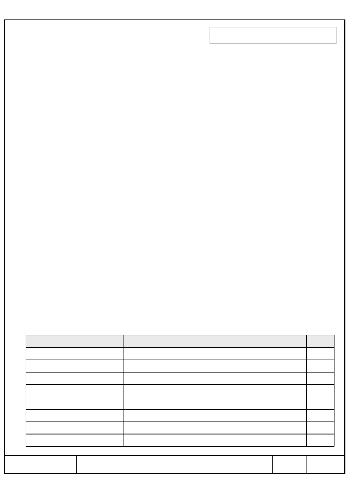
General Information
UnitSpecificationItems
mm0.300(H) x 0.300(W)Pixel Pitch
mm409.8(H) x 230.4(V)Active Display Area
Haze 25%, Hard-coating(3H)Surface Treatment
colors16.7M ( 6bit Hi-FRC )Display Colors
pixel1366 x 768Number of Pixels
RGB vertical stripePixel Arrangement
Note
Normally WhiteDisplay Mode
cd/㎡300(Typ.)Luminance of White
3/34PageLTM185AT02MODEL
Mechanical Information
PRODUCT INFORMATION
PRODUCT INFORMATION
Module
size
Note (1) Mechanical tolerance is ± 0.5mm unless there is a special comment.
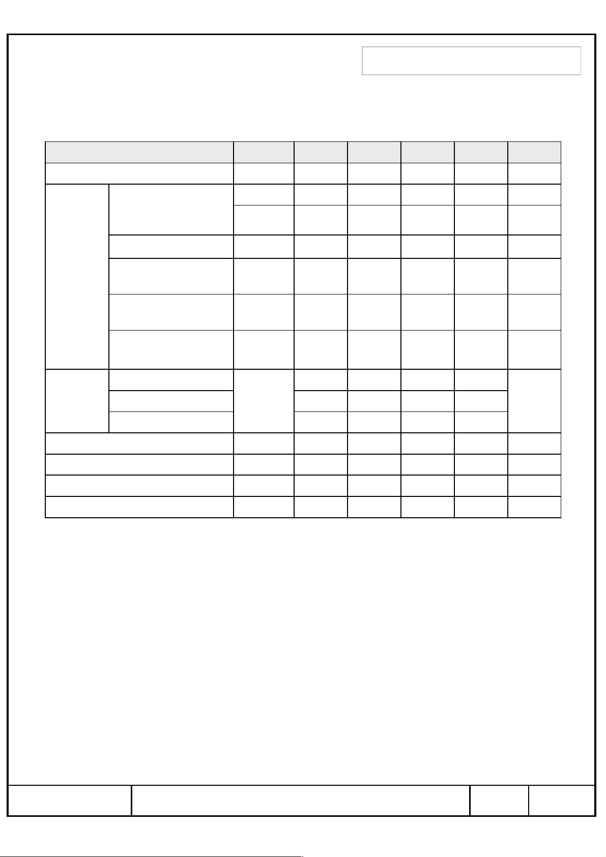
1. Absolute Maximum Ratings
Max.
430.87
255.1
16.5
2,100
NoteUnitTyp.Min.Item
mm430.37429.87Horizontal (H)
mm254.6254.1Vertical (V) w/o inverter ass’y
mm--Depth (D)
LCD module onlyg--Weight
If the condition exceeds maximum ratings, it can cause malfunction or unrecoverable
damage to the device.
NoteUnitMax.Min.SymbolItem
Power Supply Voltage
Storage temperature
Glass surface temperature
(Operation)
Shock ( non - operating )
Vibration ( non - operating )
Note (1) Ta= 25 ± 2 °C
DD
STG
OPR
nop
nop
60-25T
500T
℃
℃
(1)V6.5GND-0.5V
(2)
(2)
(3)G50-S
(4)G1.5-V
4/34PageLTM185AT02MODEL
PRODUCT INFORMATION
PRODUCT INFORMATION
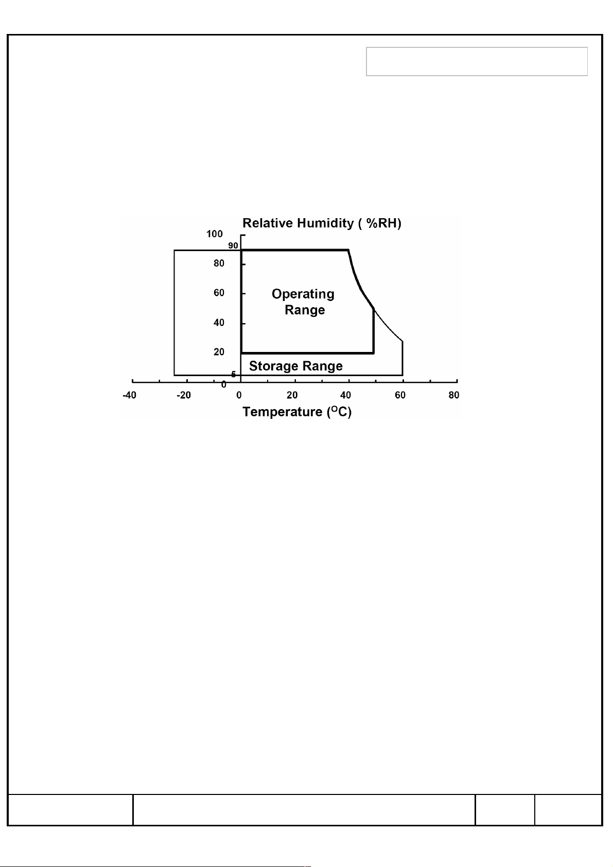
(2) Temperature and relative humidity range are shown in the figure below.
a. 90 % RH Max. (Ta ≤ 39 °C)
b. Maximum wet-bulb temperature at 39 °C or less. (Ta ≤ 39 °C)
c. No condensation
(3) 11ms, sine wave, one time for ±X, ±Y, ±Z axis
(4) 10-300 Hz, Sweep rate 10min, 30min for X,Y,Z axis
(39,90)
(39,90)
(39,90)
(39,90)
(50,50.4)
(50,50.4)
(50,50.4)
(50,50.4)
(60,27.7)
(60,27.7)
(60,27.7)
(60,27.7)
25,5)
25,5)
((--25,5)
((--25,5)
Fig. Temperature and Relative humidity range
5/34PageLTM185AT02MODEL
PRODUCT INFORMATION
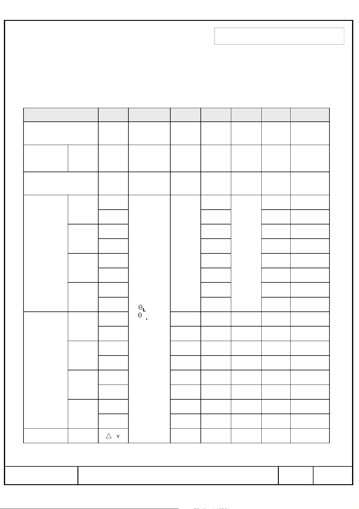
2. Optical Characteristics
PRODUCT INFORMATION
The optical characteristics should be measured in a dark room or equivalent.
Measuring equipment :
(Ta = 25 ± 2°C, VDD=5V, fv= 60Hz, fDCLK=72.33MHz, IL = 7.5mArms)
SR-3, RD-80S (TOPCON), EZ-Contrast (Eldim)
NoteUnitMax.Typ.Min.ConditionSymbolItem
Contrast Ratio
(Center of screen)
Response
Time
Luminance of White
(Center of screen)
Green
Color
Chromaticity
(CIE 1931)
Blue
White
Color
Chromaticity
(CIE 1976)
Green
Blue
Red
Red
Wx
-1000600C/R
105-Tr+ TfOn/Off
L
0.650Rx
0.335Ry
0.295Gx
0.605Gy
+0.030
-0.455-Ru'
-0.527-Rv'
-0.122-Gu'
-0.563-Gv'
-0.161-Bu'
-0.187-Bv'
Normal
θ
=0
L,R
θ
=0
U,D
Viewing
Angle
-0.030
0.145Bx
0.075By
0.313
0.329Wy
msec
cd/m2-300250Y
(3)
SR-3
(5)
RD-850S
(6)
SR-3
(7),(8)
SR-3
-0.198-Wu'
White
-0.468-Wv'
△
C.G.L
* C.G.L : Color Grayscale Linearity (continue to the next page)
u'v'White
(9)0.02--
6/34PageLTM185AT02MODEL
PRODUCT INFORMATION
PRODUCT INFORMATION
NoteUnitMax.Typ.Min.ConditionSymbolItem
%-72--Color Gamut
K-6500--Color Temperature
θ
Hor.
Viewing
Angle
Ver.
Brightness Uniformity
(9 Points)
L
θ
R
θ
U
θ
D
uni
Note (1) Test Equipment Setup
The measurement should be executed in a stable, windless and dark room between
30min after lighting the back light at the given temperature for stabilization
of the back light. This should be measured in the center of screen.
Single lamp current : 7.5mA
Environment condition : Ta = 25 ± 2 °C
CR≥10
-8070
-8070
Degrees
-8070
-8070
%25--B
(8)
EZ-
Contrast
(4)
SR-3
SR-3
Field Photodetector
1
°
TFT - LCD Module
Photodetector
Field
The center of the screen
SR-3 : 50
RD-80S : 50
㎝
LCD Panel
㎝
7/34PageLTM185AT02MODEL
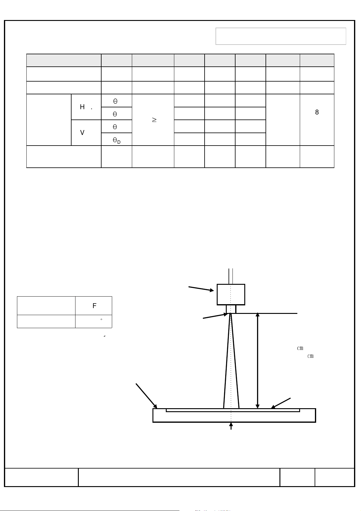
Note (2) Definition of test point
B
−
max
G
min
137 683 1229
PRODUCT INFORMATION
PRODUCT INFORMATION
Active Area
6
: Test Point
Note (3) Definition of Contrast Ratio (C/R)
: Ratio of gray max (Gmax) & gray min (Gmin) at the center point⑤ of the panel
G
CR
max
=
3 2 1
8 79
45
77
384
691
Gmax : Luminance with all pixels white
Gmin : Luminance with all pixels black
Note (4) Definition of 9 points brightness uniformity
B B
Buni
= ×
100
Bmax : Maximum brightness
Bmin : Minimum brightness
( max min)
8/34PageLTM185AT02MODEL
PRODUCT INFORMATION
PRODUCT INFORMATION
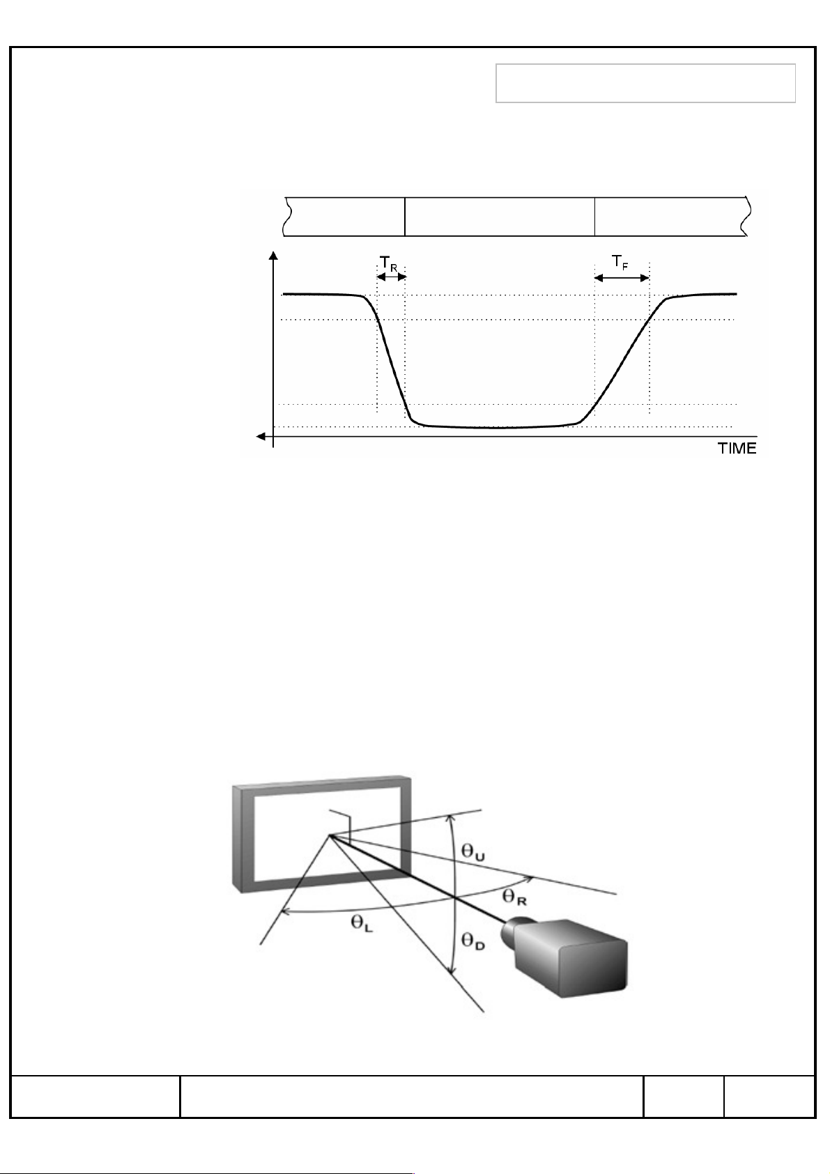
Note (5) Definition of Response time
a. On/Off response time : Sum of Tr, Tf
Display Data White(TFT off) Black(TFT on) White(TFT off)
Optical Instruments
Response
Note (6) Definition of Luminance of White : Luminance of white at center point⑤
Note (7) Definition of Color Chromaticity (CIE 1931, CIE1976)
Color coordinate of Red, Green, Blue & White at center point⑤
100%
90%
10%
0%
Note (8) Definition of Viewing Angle
: Viewing angle range (CR ≥10)
9/34PageLTM185AT02MODEL
PRODUCT INFORMATION
PRODUCT INFORMATION
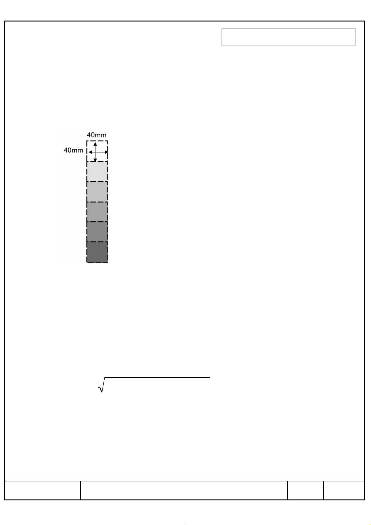
Note (9) Color Grayscale Linearity
a. Test image : 100% full white pattern with a test pattern as below
b. Test pattern : Squares, 40mm by 40mm in size, filled with 255, 225, 195, 165, 135 and
105 grays steps should be arranged at the center⑤ of the screen.
c. Test method
-1stgray step : move a square of 255 gray level should be moved into the center of the
screen and measure luminance and u’ and v’ coordinates.
- Next gray step : Move a 225 gray square into the center and measure both
luminance and coordinates, too.
d. Test evaluation
∆u' v'= (u' - u' ) + (v' - v' )
Where A, B : 2 gray levels found to have the largest color differences between them
i.e. get the largest Δu’ and Δv’ of each 6 pair of u’ and v’ and calculate the Δu’v’.
A B
2
A B
2
10/34PageLTM185AT02MODEL
3. Electrical Characteristics
3.1 TFT LCD Module
The connector for display data & timing signal should be connected.
PRODUCT INFORMATION
PRODUCT INFORMATION
Ta = 25°C
NoteUnitMax.Typ.Min.SymbolItem
Voltage of Power Supply
Differential Input
Voltage for LVDS
Receiver Threshold
LVDS
Input
Characteri
stics
LVDS skew
Differential input
voltage
Input voltage range
(single-ended)
Common mode
voltage
Current of
(a) Black
Power
Supply
Vsync Frequency
Hsync Frequency
DD
SKEW
IN
V
CM
I
DD
V
H
0+
|VID|/2
1.2
(1)V5.55.04.5V
(2)mV+100--High
mV---100Low
(3)300-300t
(4)mV600200|VID|
(4)V2.40V
2.4(4)V
|VID|/2
mA-550-
mA-400-(b) White (5),(6)
mA1000700-(c) Dot
Hz756047f
kHz59.2547.4037.13f
Main Frequency
Rush Current
DCLK
RUSH
Note (1) The ripple voltage should be controlled under 10% of VDD.
MHz90.4272.3356.66f
(7)A3--I
11/34PageLTM185AT02MODEL
 Loading...