

Page 1
Customer: GEN
Confidential
Product information
Product information
SAMSUNG TFT--
SAMSUNG TFT
SAMSUNG TFT-LCD
MODEL
MODEL
MODEL : LTA260AP05
Any modification of Specification is not allowed without SEC’s permission.
NOTE :
Customer’’
Customer
LCD
LCD
: LTA260AP05
: LTA260AP05
APPROVAED BY
s Approval
s Approval
DATE
Jun. 2, 2009
SIGNATURE
Samsung Electronics Co . , LTD.
Samsung Electronics Co . , LTD.
MODEL
MODEL LTA260AP05
MODELMODEL
LTA260AP05 Doc. No
LTA260AP05LTA260AP05
DATE
LCD Business
LCD Business
Doc. No 06
Doc. NoDoc. No
06----000
0606
PREPARED BY
000----GGGG----090602
000000
090602 Page
090602090602
DATE
Jun. 2, 2009
Page 1111 /29
PagePage
/29
/29/29
Page 2
Confidential
Contents
Revision History -------------------------------------------------------------------------------------------- (3)
General Description --------------------------------------------------------------------------------------- (4)
General Information --------------------------------------------------------------------------------------- (4)
1. Absolute Maximum Ratings -------------------------------------------------------------------------- (5)
2. Optical Characteristics --------------------------------------------------------------------------------- (7)
3. Electrical Characteristics ----------------------------------------------------------------------------- (10)
3.1 TFT LCD Module
3.2 Back Light Unit
3.3 Inverter Input & Specification
4. Block Diagram ------------------------------------------------------------------------------------------- (13)
5. Input Terminal Pin Assignment --------------------------------------------------------------------- (14)
5.1 Input Signal & Power
5.2 Inverter Input Pin Configuration
5.3 Inverter Input Power Sequence
5.4 LVDS Interface
5.5 Input Signals, Basic Display Colors and Gray Scale of Each Color
6. Interface Timing ----------------------------------------------------------------------------------------- (19)
6.1 Timing Parameters (DE only mode)
6.2 Timing Diagrams of interface Signal (DE only mode)
6.3 Power ON/OFF Sequence
7. Outline Dimension -------------------------------------------------------------------------------------- (22)
8. Reliability test -------------------------------------------------------------------------------------------- (24)
9. Packing --------------------------------------------------------------------------------------------------- (25)
10. Marking & Others ------------------------------------------------------------------------------------- (26)
11. General Precaution ----------------------------------------------------------------------------------- (27)
10.1 Handling
10.2 Storage
10.3 Operation
10.4 Operation Condition Guide
10.5 Others
MODEL
MODEL LTA260AP05
MODELMODEL
LTA260AP05 Doc. No
LTA260AP05LTA260AP05
Doc. No 06
Doc. NoDoc. No
06----000
0606
000----GGGG----090602
000000
090602 Page
090602090602
Page 2222 /29
PagePage
/29
/29/29
Page 3
Revision History
Date Rev. No Page Summary
Jun. 2, 2009 000 all First issued
Confidential
MODEL
MODEL LTA260AP05
MODELMODEL
LTA260AP05 Doc. No
LTA260AP05LTA260AP05
Doc. No 06
Doc. NoDoc. No
06----000
0606
000----GGGG----090602
000000
090602 Page
090602090602
Page 3333 /29
PagePage
/29
/29/29
Page 4
Confidential
General Description
Description
LTA260AP05 is a color active matrix liquid crystal display (LCD) that uses amorphous
silicon TFT (Thin Film Transistor) as switching components. This model is composed of a
TFT LCD panel, a driver circuit and a back light unit. The resolution of a 26.0” is
1366 x 768 and this model can display up to 16.7 million colors with wide viewing angle of
89° or higher in all directions. This panel is intended to support applications to provide a
excellent performance for Flat Panel Display such as Home-alone Multimedia TFT-LCD
TV and High Definition TV.
Features
RoHS compliance (Pb-free)
High contrast & aperture ratio with wide color gamut
APVA( Advanced Patterned Vertical Align) mode
Wide viewing angle (±178°)
High speed response
HD resolution (16:9)
Low Power consumption
U-Type 4 CCFLs (Cold Cathode Fluorescent Lamp)
DE(Data Enable) mode
LVDS (Low Voltage Differential Signaling) interface (1pixel/clock)
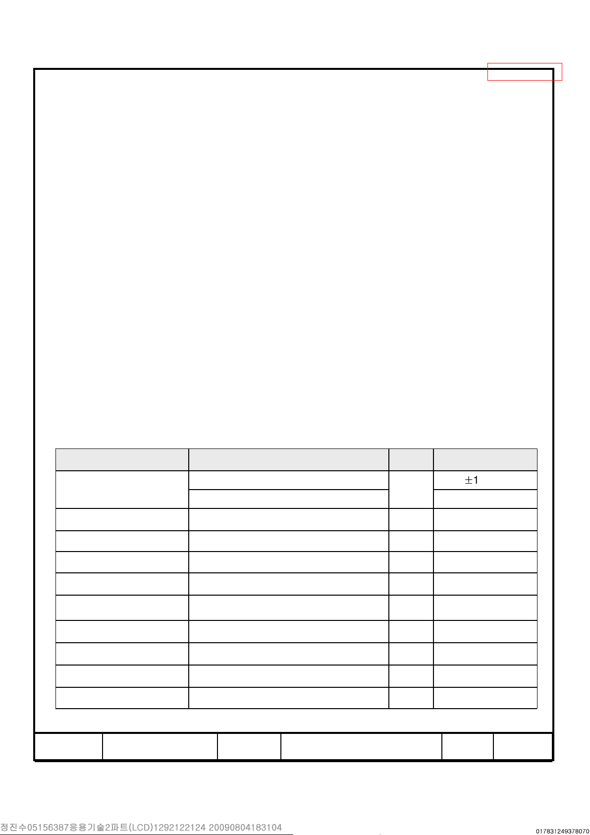
General Information
Items Specification Unit Note
Module Size
Weight 5,500 (Max) g
Pixel Pitch 0.4215(H) x 0.4215(V) mm
Active Display Area 575.769(H) x 323.712(V) mm
Surface Treatment Haze 14% , Hard-coating (3H) -
Display Colors 8 bit - 16.7M colors
Number of Pixels 1366 x 768 pixel
Pixel Arrangement RGB Horizontal stripe -
Display Mode Normally Black -
Luminance of White 450 (Typ.) cd/m
626.0(H
) x 373.0(V
TYP
48.6(D
MAX
)
TYP
)
mm
2
±
1.0mm
MODEL
MODEL LTA260AP05
MODELMODEL
LTA260AP05 Doc. No
LTA260AP05LTA260AP05
Doc. No 06
Doc. NoDoc. No
06----000
0606
000----GGGG----090602
000000
090602 Page
090602090602
Page 4444 /29
PagePage
/29
/29/29
Page 5
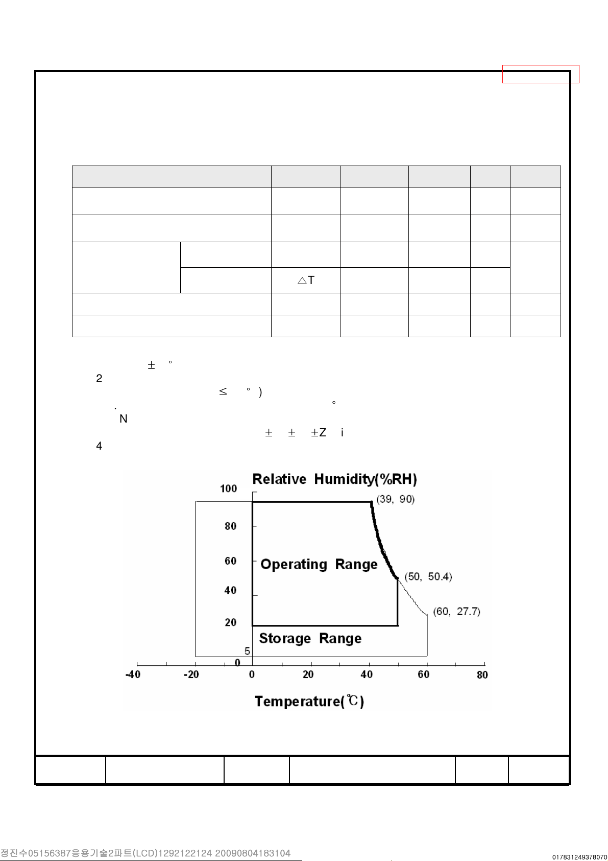
1. Absolute Maximum Ratings
If the condition exceeds maximum ratings, it can cause malfunction or unrecoverable
damage to the device.
Item Symbol Min. Max. Unit Note
Confidential
Power Supply Voltage V
Storage temperature T
Glass surface
Center T
DD
STG
OPR
GND-0.5 13.2 V (1)
-20 60
0 50
temperature
△
(Operation)
T. Uniformity
Shock ( non - operating ) S
Vibration ( non - operating ) V
Note (1) Ta= 25 ±2 °C
(2) Temperature and relative humidity range are shown in the figure below.
a. 90 % RH Max. (Ta ≤39°C)
b. Relative Humidity is 90% or less. (Ta > 39°C)
c. No condensation
(3) 11ms, sine wave, one time for ±X, ±Y, ±Z axis
(4) 10-300 Hz, Sweep rate 10min, 30min for X,Y,Z axis
T
nop
nop
- 10
- 50 G (3)
- 1.5 G (4)
℃
℃
℃
(2)
(2),(5)
Fig. Temperature and Relative humidity range
MODEL
MODEL LTA260AP05
MODELMODEL
LTA260AP05 Doc. No
LTA260AP05LTA260AP05
90
Doc. No 06
Doc. NoDoc. No
06----000
000----GGGG----090602
0606
000000
090602 Page
090602090602
Page 5555 /29
PagePage
/29
/29/29
Page 6
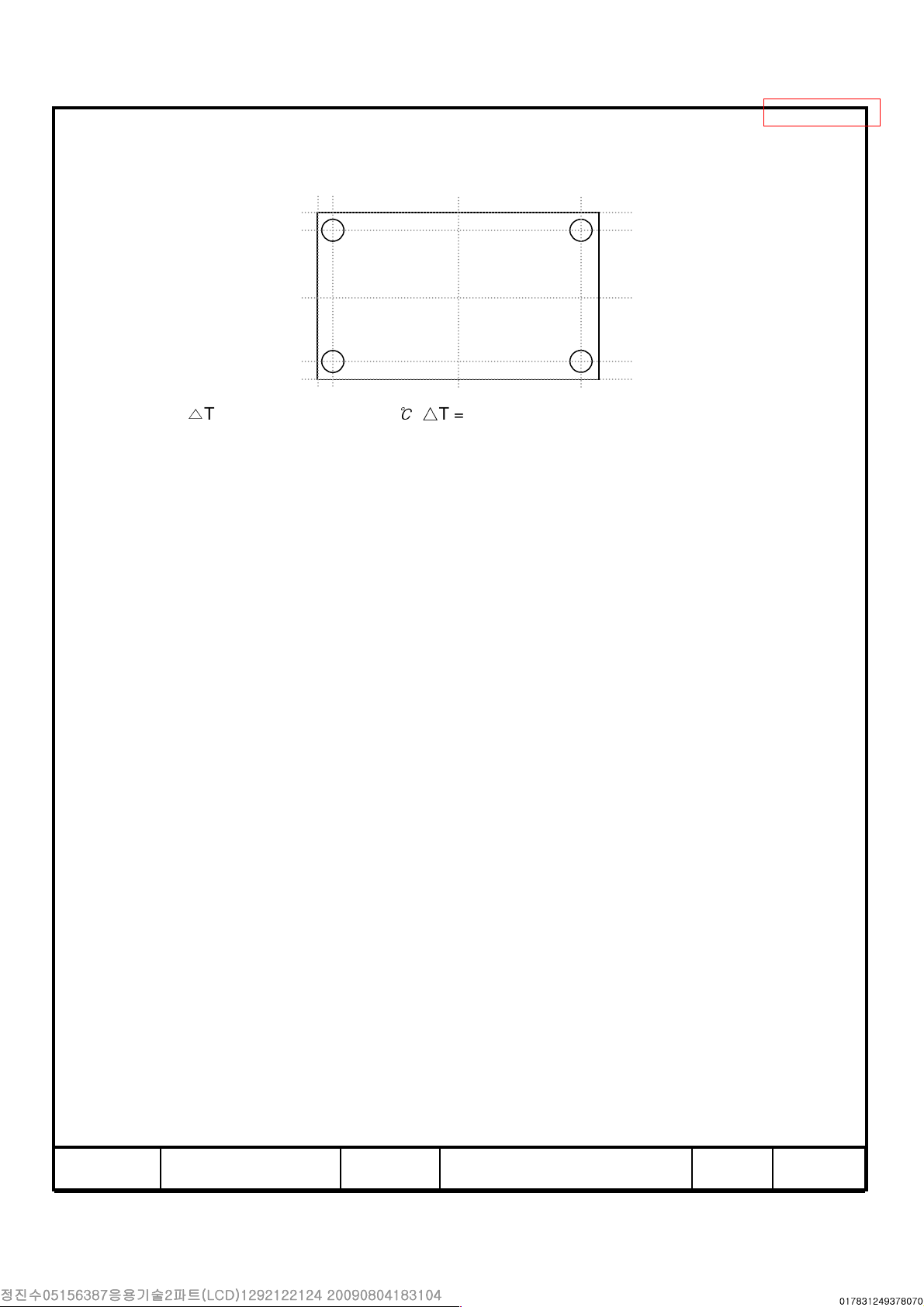
(5) Definition of test point
5mm
Confidential
5mm
1 2
5
○
LCD Module (Active)
MAX
4
| )
3
△
T should be less than 10 ℃(△T = | T
T
T1~ T4 : Temperature of each edge of the glass surface
: Temperature of the center of the glass surface (Test point 5)
OPR
T
: The highest temperature of the glass surface
MAX
OPR
– T
MODEL
MODEL LTA260AP05
MODELMODEL
LTA260AP05 Doc. No
LTA260AP05LTA260AP05
Doc. No 06
Doc. NoDoc. No
06----000
0606
000----GGGG----090602
000000
090602 Page
090602090602
Page 6666 /29
PagePage
/29
/29/29
Page 7
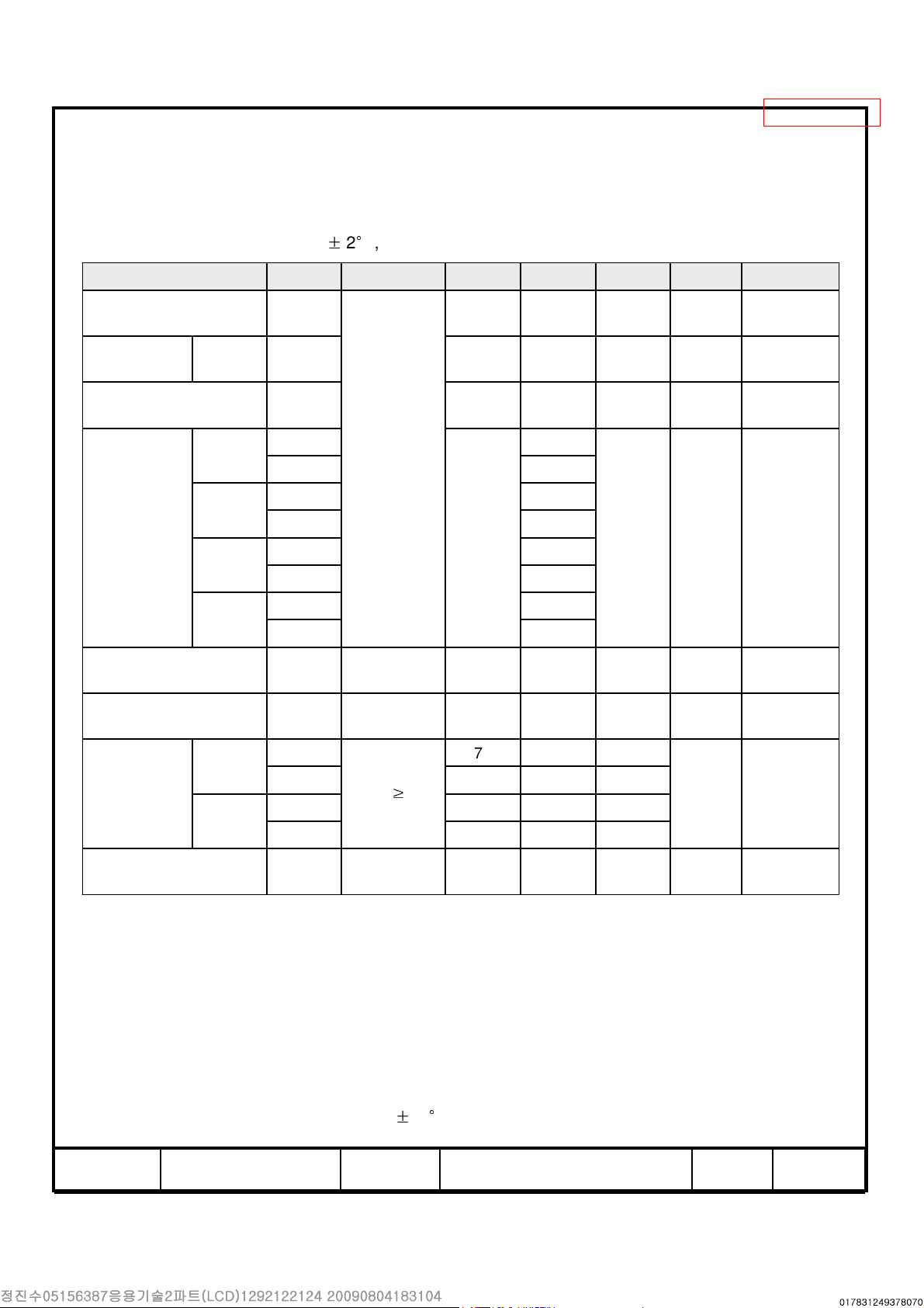
2. Optical Characteristics
The optical characteristics should be measured in a dark room or equivalent.
Measuring equipment :
TOPCON RD-80S,TOPCON SR-3, ELDIM EZ-Contrast
Confidential
(Ta = 25 ±2°C, VDD=12V, fv= 60Hz, f
Item Symbol Condition Min. Typ. Max. Unit Note
Contrast Ratio
(Center of screen)
Response
Time
Luminance of White
(Center of screen)
Color
Chromaticity
(CIE 1931)
Color Gamut - - 72 - %
G-to-G
(Avg)
Red
Green
Blue
White
C/R
Tg - 8 16
Y
L
Rx
Ry 0.337
Gx 0.283
Gy 0.597
Bx 0.146
By 0.071
Wx 0.280
Wy 0.290
Normal
θL,R=0
θU,D=0
Viewing
Angle
3,500 4,000 -
400 450 - cd/m
0.646
TYP.
-0.03
=78MHz, Dimming voltage=3.3V)
DCLK
TYP.
+0.03
(1)
SR-3
(3)
RD-80S
2
(4)
SR-3
(5),(6)
SR-3
(5)
SR-3
Color Temperature - - 10,000 - K
Hor.
Viewing
Angle
Ver.
Brightness Uniformity
(9 Points)
θ
L
θ
R
θ
U
θ
D
B
uni
C/R≥10
79 89 -
79 89 -
Degree
79 89 -
79 89 -
- - 25 %
- Test Equipment Setup
The measurement should be executed in a stable, windless and dark room between
40min and 60min after lighting the back light at the given temperature for stabilization
of the back light. This should be measured in the center of screen.
Dimming voltage =3.3V
Environment condition : Ta = 25 ±2 °C
(5)
SR-3
(6)
EZ-Contrast
(2)
SR-3
MODEL
MODEL LTA260AP05
MODELMODEL
LTA260AP05 Doc. No
LTA260AP05LTA260AP05
Doc. No 06
Doc. NoDoc. No
06----000
0606
000----GGGG----090602
000000
090602 Page
090602090602
Page 7777 /29
PagePage
/29
/29/29
Page 8
Confidential
G
min
Photo detector Field
SR-3 1
RD-80S 2
TFT - LCD Module
- Definition of test point
228 683 1138
Photo detector
°
°
Field
The center of the screen
SR-3 : 50
RD-80S : 50
EZ-Contrast :0
㎝
LCD Panel
㎝
㎝
128
384
640
Note (1) Definition of Contrast Ratio (C/R)
: Ratio of gray max (Gmax) & gray min (Gmin) at the center point ⑤of the panel
C R
/
=
⑨⑨⑨⑨
⑥⑥⑥⑥
G
max
Gmax : Luminance with all pixels white
Gmin : Luminance with all pixels black
⑧⑧⑧⑧
⑤⑤⑤⑤ ④④④④
⑦⑦⑦⑦
①①①①②②②②③③③③
Active Area
Test Point
MODEL
MODEL LTA260AP05
MODELMODEL
LTA260AP05 Doc. No
LTA260AP05LTA260AP05
Doc. No 06
Doc. NoDoc. No
06----000
0606
000----GGGG----090602
000000
090602 Page
090602090602
Page 8888 /29
PagePage
/29
/29/29
Page 9
Note (2) Definition of 9 points brightness uniformity ( Test pattern : Full White )
B
−
max
B B
Buni
= ∗
Bmax : Maximum brightness
Bmin : Minimum brightness
Note (3) Definition of Response time : Sum of Tr, Tf
( max min)
100
Confidential
Display data
Optical Instruments
Response
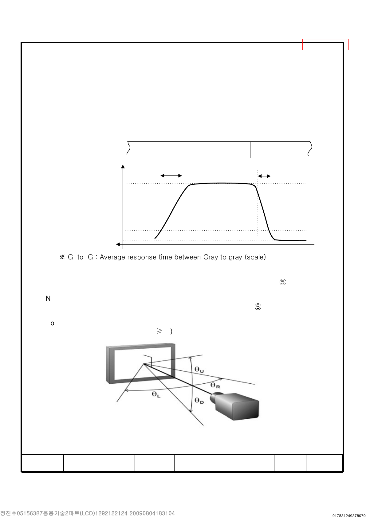
※ G-to-G : Average response time between Gray to gray (scale)
Note (4) Definition of Luminance of White : Luminance of white at center point
Note (5) Definition of Color Chromaticity (CIE 1931)
Color coordinate of Red, Green, Blue & White at center point
Note (6) Definition of Viewing Angle
: Viewing angle range (C/R ≥10)
100%
90%
10%
0%
Black (data
off)
T
R
White (data on)
Black (data off)
T
F
⑤
TIME
⑤
MODEL
MODEL LTA260AP05
MODELMODEL
LTA260AP05 Doc. No
LTA260AP05LTA260AP05
Doc. No 06
Doc. NoDoc. No
06----000
0606
000----GGGG----090602
000000
090602 Page
090602090602
Page 9999 /29
PagePage
/29
/29/29
Page 10

Confidential
3. Electrical Characteristics
3.1 TFT LCD Module
The connector for display data & timing signal should be connected.
Ta = 25°C ± 2 °C
Item Symbol Min. Typ. Max. Unit Note
Voltage of Power Supply V
Current
of Power
Supply
(a) Black
(b) White 205 305 405 mA
(c) V-Stripe 459 559 659 mA
Vsync Frequency f
Hsync Frequency f
Main Frequency f
Rush Current I
DD
I
DD
V
H
DCLK
RUSH
10.8 12.0 13.2 V (1)
213 313 413 mA
48 60 66 Hz
44 48 53 kHz
72 78 85 MHz
- - 4 A (4)
Note (1) The ripple voltage should be controlled under 10% of VDD.
(2) fV=60Hz, f
DCLK
= 78MHz, VDD= 12.0V, DC Current.
(3) Power dissipation check pattern (LCD Module only)
a) Black Pattern b) White Pattern c) V-stripe
(2),(3)
(4) Measurement Conditions
100%
90%
10%
GND
Rush Current I
MODEL
MODEL LTA260AP05
MODELMODEL
LTA260AP05 Doc. No
LTA260AP05LTA260AP05
RUSH
T
=470
RUSH
㎲
can be measured when T
Doc. No 06
Doc. NoDoc. No
06----000
0606
. is 470㎲.
RUSH
000----GGGG----090602
000000
090602 Page
090602090602
V
DD
Page 10
PagePage
10 /29
/29
1010
/29/29
Page 11

3.2 Back Light Unit
The back light unit contains 4 U-type CCFLs ( Cold Cathode Fluorescent
Lamp ). The characteristics of lamps are shown in the following tables.
Socket
HOT 1
HOT 2
LCD
Inverter
Module
Confidential
Ta=25 ± 2°C
Lamp 1
HOT 7
Lamp 4
HOT 8
Item Symbol Min. Typ. Max. Unit Note
Operating Life Time Hr 50,000 - - Hour (1)
Note (1) It is defined as the time to take until the brightness reduces to 50% of its original value.
[Operating condition : Ta = 25±2℃, IL= 12mA , For single lamp only. ]
MODEL
MODEL LTA260AP05
MODELMODEL
LTA260AP05 Doc. No
LTA260AP05LTA260AP05
Doc. No 06
Doc. NoDoc. No
06----000
0606
000----GGGG----090602
000000
090602 Page
090602090602
Page 11
PagePage
11 /29
1111
/29
/29/29
Page 12

3.3 Inverter Input Condition & Specification
Items Symbol Conditions
Min. Typ. Max.
Confidential
Specifications
Unit Note
Input
Voltage
Input
Current
Frequency F
Lamp
current
Backlight
On/Off
PWM
dimming
Dimming
Control
Note) Power Consumption is measured when 500[cd/m2] of luminance which is the typical luminance.
Vin - 22 24 26 V Ta=25
Iin
LAMP
I
O
ON Vin=24.0 V 2.4 - 5.25
OFF Vin=24.0 V 0 - 0.8
F
PMD
V
DIM
Vin=24.0V
Vdim=3.3V
Vin=24.0 V 60 62 64 kHz
Vin=24.0V
Vdim=3.3V
Vin=24.0V,
Vadim=3.3V
Min. Lum - - 0
11.5 12.0 12.5 mArms
140 150 160 Hz
2.4 Adc (1)
--3.3Max Lum
After 2 Hours
Warm-Up
@Vin=24V
V -
±2 °C
-V
Lamp Current is measured at the point before Lamp.
(1) Max Value of the Power Consumption is measured after 120 min warm-up.
.
MODEL
MODEL LTA260AP05
MODELMODEL
LTA260AP05 Doc. No
LTA260AP05LTA260AP05
Doc. No 06
Doc. NoDoc. No
06----000
000----GGGG----090602
0606
000000
090602 Page
090602090602
Page 12
PagePage
12 /29
1212
/29
/29/29
Page 13

4. Block Diagram
CONTROL PCB
Confidential
USER CONNECTOR
DC/DC STEP DOWN
DC/DC CONVERTOR
(AVDD/VDD/VON/V
DATA
CONTROL
VIN(5.0V)
AV
DD
VON/V
OFF
V
COM
Y VOLTAGE
VDD(3.3V)
VDD(2.5V)
OFF
TIMING CONTROLLER
MEMORY(DCC)
FPC
FPC
FPCFPC
)
GAMMA-GENERATOR
V
-GENERATOR
COM
SOURCE
PCB
DATA DRIVER
IC
LTA260AP05
PANEL
MODEL
MODEL LTA260AP05
MODELMODEL
LTA260AP05 Doc. No
LTA260AP05LTA260AP05
Doc. No 06
Doc. NoDoc. No
06----000
0606
000----GGGG----090602
000000
090602 Page
090602090602
Page 13
PagePage
13 /29
1313
/29
/29/29
Page 14

Confidential
5. Input Terminal Pin Assignment
5.1. Input Signal & Power Connector : IS100-L30O-C23 (UJUELE)
PIN No. Description PIN No. Description
1 No Connection (Note1) 16 GND
2 No Connection (Note1) 17 RxIN3-
3 No Connection (Note1) 18 RxIN3+
4 GND 19 GND
5 RxIN0- 20 No Connection (Note1)
6 RxIN0+ 21 LVDS OPTION (Note 2)
7 GND 22 No Connection (Note1)
8 RxIN1- 23 GND
9 RxIN1+ 24 GND
10 GND 25 No Connection (Note1)
11 RxIN2- 26 Vin
12 RxIN2+ 27 Vin
13 GND 28 Vin
14 RxCLK- 29 Vin
15 RxCLK+ 30 Vin
Note1) No Connection: This PINS are only used ONLY for SAMSUNG.
Note2) LVDS OPTION : If this PIN is HIGH (3.3 V) →VESA LVDS format
LOW (GND) →JEIDA LVDS format
SEQUENCE : On = VDD(T1)
OFF = Interface Signal(T3)
≥≥≥≥
LVDS Option
≥≥≥≥
Interface Signal(T2)
≥≥≥≥
LVDS Option
≥≥≥≥
V
DD
MODEL
MODEL LTA260AP05
MODELMODEL
LTA260AP05 Doc. No
LTA260AP05LTA260AP05
Doc. No 06
Doc. NoDoc. No
06----000
0606
000----GGGG----090602
000000
090602 Page
090602090602
Page 14
PagePage
14 /29
1414
/29
/29/29
Page 15

Note(1) Pin number starts from Left side
▼
Pin No. 1 Pin No. 30
#1 #30
Confidential
PCB
#1
Fig. Connector diagram
a. Power GND pins should be connected to the LCD’s metal chassis.
b. All power input pins should be connected together.
c. All NC pin should be separated from other signal or power.
#30
MODEL
MODEL LTA260AP05
MODELMODEL
LTA260AP05 Doc. No
LTA260AP05LTA260AP05
Doc. No 06
Doc. NoDoc. No
06----000
0606
000----GGGG----090602
000000
090602 Page
090602090602
Page 15
PagePage
15 /29
1515
/29
/29/29
Page 16

5.2. Inverter Input Pin Configuration
Connector : 20022WR-14AML (YEONHO)
Pin No. Pin Configuration (FUNCTION)
1 Vin (24 V)
2 Vin (24 V)
3 Vin (24 V)
4 Vin (24 V)
5 Vin (24 V)
6 GND
7 GND
8 GND
9 GND
10 GND
11 No Connection
12 Backlight On /Off [ON:2.4 – 5.25 V, OFF: 0 - 0.8 V]
Confidential
13 Dimming Control [0V:Min, 3.3V:Max]
14 No Connection
5.3. Inverter Input Power Sequence
0.9 Vin
Vin (24V)
Dimming Control
( 0 ~ 3.3 V )
0.5sec [Min]
Backlight On/Off
0.1 Vin
0.02sec [Min]
0.9 Vin
0.5sec [Min]
2.4V(On level)
0.8V(Off level)
MODEL
MODEL LTA260AP05
MODELMODEL
LTA260AP05 Doc. No
LTA260AP05LTA260AP05
0.5sec [Min]
Doc. No 06
Doc. NoDoc. No
0.1sec [Min]
06----000
000----GGGG----090602
0606
000000
090602 Page
090602090602
Page 16
PagePage
16 /29
/29
1616
/29/29
Page 17

5.4 LVDS Interface
- LVDS Receiver : Tcon (merged)
- Data Format (JEIDA & VESA)
TxIN/RxOUT0 R2 R0
TxIN/RxOUT1 R3 R1
TxIN/RxOUT2 R4 R2
Confidential
LVDS pin JEIDA -DATA VESA -DATA
TxOUT/RxIN0
TxOUT/RxIN1
TxOUT/RxIN2
TxIN/RxOUT3 R5 R3
TxIN/RxOUT4 R6 R4
TxIN/RxOUT6 R7 R5
TxIN/RxOUT7 G2 G0
TxIN/RxOUT8 G3 G1
TxIN/RxOUT9 G4 G2
TxIN/RxOUT12 G5 G3
TxIN/RxOUT13 G6 G4
TxIN/RxOUT14 G7 G5
TxIN/RxOUT15 B2 B0
TxIN/RxOUT18 B3 B1
TxIN/RxOUT19 B4 B2
TxIN/RxOUT20 B5 B3
TxIN/RxOUT21 B6 B4
TxIN/RxOUT22 B7 B5
TxOUT/RxIN3
MODEL
MODEL LTA260AP05
MODELMODEL
LTA260AP05 Doc. No
LTA260AP05LTA260AP05
TxIN/RxOUT24 HSYNC HSYNC
TxIN/RxOUT25 VSYNC VSYNC
TxIN/RxOUT26 DEN DEN
TxIN/RxOUT27 R0 R6
TxIN/RxOUT5 R1 R7
TxIN/RxOUT10 G0 G6
TxIN/RxOUT11 G1 G7
TxIN/RxOUT16 B0 B6
TxIN/RxOUT17 B1 B7
TxIN/RxOUT23 RESERVED RESERVED
Doc. No 06
Doc. NoDoc. No
06----000
000----GGGG----090602
0606
000000
090602 Page
090602090602
Page 17
PagePage
17 /29
/29
1717
/29/29
Page 18

5.5 Input Signals, Basic Display Colors and Gray Scale of Each Color
Confidential
COLOR
BASIC
COLOR
GRAY
SCALE
OF
RED
GRAY
SCALE
OF
GREEN
GRAY
SCALE
OF
BLUE
DATA SIGNAL
DISPLAY
(8bit)
R0 R1 R2 R3 R4 R5 R6 R7 G0 G1 G2 G3 G4 G5 G6 G7 B0 B1 B2 B3 B4 B5 B6 B7
BLACK 0 0 0 0 0 0 0 0 0 0 0 0 0 0 0 0 0 0 0 0 0 0 0 0 -
BLUE 0 0 0 0 0 0 0 0 0 0 0 0 0 0 0 0 1 1 1 1 1 1 1 1 -
GREEN 0 0 0 0 0 0 0 0 1 1 1 1 1 1 1 1 0 0 0 0 0 0 0 0 -
CYAN 0 0 0 0 0 0 0 0 1 1 1 1 1 1 1 1 1 1 1 1 1 1 1 1 -
RED 1 1 1 1 1 1 1 1 0 0 0 0 0 0 0 0 0 0 0 0 0 0 0 0 -
MAGENTA 1 1 1 1 1 1 1 1 0 0 0 0 0 0 0 0 1 1 1 1 1 1 1 1 -
YELLOW 1 1 1 1 1 1 1 1 1 1 1 1 1 1 1 1 0 0 0 0 0 0 0 0 -
WHITE 1 1 1 1 1 1 1 1 1 1 1 1 1 1 1 1 1 1 1 1 1 1 1 1 -
BLACK 0 0 0 0 0 0 0 0 0 0 0 0 0 0 0 0 0 0 0 0 0 0 0 0 R0
1 0 0 0 0 0 0 0 0 0 0 0 0 0 0 0 0 0 0 0 0 0 0 0 R1
DARK
↑
↓
LIGHT
RED 1 1 1 1 1 1 1 1 0 0 0 0 0 0 0 0 0 0 0 0 0 0 0 0 R255
BLACK 0 0 0 0 0 0 0 0 0 0 0 0 0 0 0 0 0 0 0 0 0 0 0 0 G0
DARK
↑
↓
LIGHT
GREEN 0 0 0 0 0 0 0 0 1 1 1 1 1 1 1 1 0 0 0 0 0 0 0 0 G255
BLACK 0 0 0 0 0 0 0 0 0 0 0 0 0 0 0 0 0 0 0 0 0 0 0 0 B0
DARK
↑
↓
LIGHT
BLUE 0 0 0 0 0 0 0 0 0 0 0 0 0 0 0 0 1 1 1 1 1 1 1 1 B255
0 1 0 0 0 0 0 0 0 0 0 0 0 0 0 0 0 0 0 0 0 0 0 0 R2
: : : : : : : : : : : : : : : : : :
: : : : : : : : : : : : : : : : : :
1 0 1 1 1 1 1 1 0 0 0 0 0 0 0 0 0 0 0 0 0 0 0 0 R253
0 1 1 1 1 1 1 1 0 0 0 0 0 0 0 0 0 0 0 0 0 0 0 0 R254
0 0 0 0 0 0 0 0 1 0 0 0 0 0 0 0 0 0 0 0 0 0 0 0 G1
0 0 0 0 0 0 0 0 0 1 0 0 0 0 0 0 0 0 0 0 0 0 0 0 G2
: : : : : : : : : : : : : : : : : :
: : : : : : : : : : : : : : : : : :
0 0 0 0 0 0 0 0 1 0 1 1 1 1 1 1 0 0 0 0 0 0 0 0 G253
0 0 0 0 0 0 0 0 0 1 1 1 1 1 1 1 0 0 0 0 0 0 0 0 G254
0 0 0 0 0 0 0 0 0 0 0 0 0 0 0 0 1 0 0 0 0 0 0 0 B1
0 0 0 0 0 0 0 0 0 0 0 0 0 0 0 0 0 1 0 0 0 0 0 0 B2
: : : : : : : : : : : : : : : : : :
: : : : : : : : : : : : : : : : : :
0 0 0 0 0 0 0 0 0 0 0 0 0 0 0 0 1 0 1 1 1 1 1 1 B253
0 0 0 0 0 0 0 0 0 0 0 0 0 0 0 0 0 1 1 1 1 1 1 1 B254
RED GREEN BLUE
GRAY
SCALE
LEVEL
R252
G252
B252
R3~
G3~
B3~
Note) Definition of Gray :
Rn : Red Gray, Gn : Green Gray, Bn : Blue Gray (n = Gray level)
Input Signal : 0 = Low level voltage, 1 = High level voltage
MODEL
MODEL LTA260AP05
MODELMODEL
LTA260AP05 Doc. No
LTA260AP05LTA260AP05
Doc. No 06
Doc. NoDoc. No
06----000
0606
000----GGGG----090602
000000
090602 Page
090602090602
Page 18
PagePage
18 / 28
18 /29
1818
/29
/29/29
Page 19

Confidential
6. Interface Timing
6.1 Timing Parameters ( DE only mode )
SIGNAL ITEM SYMBOL MIN. TYP. MAX. Unit NOTE
Clock
Hsync F
Vsync F
Vertical
Display Term
Horizontal
Display Term
Frequency
Active
Display
Period
Vertical
Total
Active
Display
Period
Horizontal
Total
1/T
T
T
T
T
VD
HD
C
H
V
V
H
72 78 85 MHz -
44 48 53 KHz -
48 60 66 Hz -
- 768 - lines -
773 802 1200 lines -
- 1366 - clocks -
1460 1624 2000 clocks -
Note) This product is DE only mode. The input of Hsync & Vsync signal does
not have an effect on normal operation.
(1) Test Point : TTL control signal and CLK at LVDS Tx input terminal in system
(2) Internal VDD= 3.3V
MODEL
MODEL LTA260AP05
MODELMODEL
LTA260AP05 Doc. No
LTA260AP05LTA260AP05
Doc. No 06
Doc. NoDoc. No
06----000
0606
000----GGGG----090602
000000
090602 Page
090602090602
Page 19
PagePage
19 /29
1919
/29
/29/29
Page 20

6.2 Timing diagrams of interface signal ( DE only mode )
T
V
T
VD
DE
T
H
T
HD
DE
Confidential
D
CLK
DATA
SIGNALS
T
C
MODEL
MODEL LTA260AP05
MODELMODEL
LTA260AP05 Doc. No
LTA260AP05LTA260AP05
Doc. No 06
Doc. NoDoc. No
06----000
0606
000----GGGG----090602
000000
090602 Page
090602090602
Page 20
PagePage
20 /29
2020
/29
/29/29
Page 21

6.3 Power ON/OFF Sequence
To prevent a latch-up or DC operation of the LCD Module, the power on/off
sequence should be as the diagram below.
0<T1≤10ms
0<T2≤50ms
0<T3≤50ms
1000ms≤T4
Confidential
1000ms≤T5
(Recommend Value)
100ms≤T6
(Recommend Value)
T1 : VDDrising time from 10% to 90%
T2 : The time from VDDto valid data at power ON.
T3 : The time from valid data off to VDDoff at power Off.
T4 : VDDoff time for Windows restart
T5 : The time from valid data to B/L enable at power ON.
T6 : The time from valid data off to B/L disable at power Off.
The supply voltage of the external system for the Module input should be the same
as the definition of VDD.
Apply the lamp voltage within the LCD operation range. When the back light turns on
before the LCD operation or the LCD turns off before the back light turns off,
the display may momentarily show abnormal screen.
In case of VDD= off level,
please keep the level of input signals low or keep a high impedance.
T4 should be measured after the Module has been fully discharged between power off
and on period.
Interface signal should not be kept at high impedance when the power is on.
MODEL
MODEL LTA260AP05
MODELMODEL
LTA260AP05 Doc. No
LTA260AP05LTA260AP05
Doc. No 06
Doc. NoDoc. No
06----000
0606
000----GGGG----090602
000000
090602 Page
090602090602
Page 21
PagePage
21 /29
2121
/29
/29/29
Page 22

Page 23

Page 24

9. PACKING
9.1 CARTON (Internal Package)
(1) Packing Form
Corrugated fiberboard box and corrugated cardboard as shock absorber
(2) Packing Method
Confidential
Packing
-Pallet Box
Cushion-Foam
LCD Module
Cushion-Foam
Cushion-Foam
LCD Module
Cushion-Foam
Pallet-Plastic
9.2 Packing Specification
Item Specification Remark
Direction to open
LCD Packing
Pallet 1Box / Pallet
Packing Direction Vertical
Total Pallet Size H x V x height 1150mm(H) x 985mm(V) x 1054mm(height)
Total Pallet Weight 133.8 kg
MODEL
MODEL LTA260AP05
MODELMODEL
LTA260AP05 Doc. No
LTA260AP05LTA260AP05
24ea / (Packing-
Pallet Box)
Doc. No 06
Doc. NoDoc. No
1. 4.5 Kg / LCD (1ea)
2. 2.7 Kg / Cushion-pallet (1ea)
3. 7.0 Kg / Packing-Pallet Box (1ea)
4. Cushion-pallet Material : EPS
5. Packing-Pallet Box Material : DW4
1. Pallet weight = 8kg
2. 8Kg/Pallet
Pallet(8kg) + Module(4.5kg*24ea=108) +
Cushion(2.7kg*4ea=10.8kg) + PalletBOX(7.0kg)
06----000
000----GGGG----090602
0606
000000
090602 Page
090602090602
Page 24
PagePage
24 /29
/29
2424
/29/29
Page 25

10. MARKING & OTHERS
A nameplate bearing followed by is affixed to a shipped product at the specified
location on each product.
(1) Parts number : LTA260AP05
(2) Revision: Three letters
(3) Lot number : X X X X XXX XX X
Cell Position No. (In the Glass)
Glass No. (In the one Lot)
Lot No. (Glass)
Month
Year (Note1)
Product code
Line
(4) Nameplate Indication
Confidential
LTA260AP05
0730
XXXXXXXXXX XXX
(5) Packing box attach
LTA260AP05
Week code : 05 29
week
year
40mm
Revision code
Lot number
80mm
100mm
Part number
XXXX
24
Box serial number
(6) Others
1. After service part
Lamps cannot be replaced because of the narrow bezel structure.
MODEL
MODEL LTA260AP05
MODELMODEL
LTA260AP05 Doc. No
LTA260AP05LTA260AP05
165mm
Doc. No 06
Doc. NoDoc. No
06----000
000----GGGG----090602
0606
000000
090602 Page
090602090602
Page 25
PagePage
25 /29
/29
2525
/29/29
Page 26

11. General Precautions
11.1 Handling
(a) When the Module is assembled, it should be attached to the system firmly
using all mounting holes. Be careful not to twist and bend the Module.
(b) Because the inverter use high voltage, it should be disconnected from power
before it is assembled or disassembled.
(c) Refrain from strong mechanical shock and / or any force to the Module.
In addition to damage, this may cause improper operation or damage to the Module
and CCFL back light.
(d) Note that polarizers are very fragile and could be damage easily.
Do not press or scratch the surface harder than a HB pencil lead.
(e) Wipe off water droplets or oil immediately. If you leave the droplets for a long
time, staining or discoloration may occur.
(f) If the surface of the polarizer is dirty, clean it using absorbent cotton or soft cloth.
Confidential
(g) Desirable cleaners are water, IPA(Isopropyl Alcohol) or Hexane.
Do not use Ketone type materials(ex. Acetone), Ethyl alcohol, Toluene, Ethyl acid
or Methyl chloride. It might permanent damage to the polarizer due to chemical
reaction.
(h) If the liquid crystal material leaks from the panel, it should be kept away
from the eyes or mouth . In case of contact with hands, legs or clothes, it must
be washed away with soap thoroughly.
(i) Protect the module from Electrostatic discharge. Otherwise the ASIC IC or
Semiconductor would be damaged
(j) Use finger-stalls with soft gloves in order to keep display clean during the
incoming inspection and assembly process.
(k) Do not disassemble the Module.
(l) Do not disassemble shield case of inverter & LVDS board.
(m) Do not connect N.C pins. (Samsung internal use only)
(n) Protection film for polarizer on the Module should be slowly peeled off just before use
so that the electrostatic charge can be minimized. Must put on antistatic glove while
handle a module
.
(o) Pins of I/F connector should not be touched directly with bare hands.
MODEL
MODEL LTA260AP05
MODELMODEL
LTA260AP05 Doc. No
LTA260AP05LTA260AP05
Doc. No 06
Doc. NoDoc. No
06----000
000----GGGG----090602
0606
000000
090602 Page
090602090602
Page 26
PagePage
26 /29
2626
/29
/29/29
Page 27

Confidential
11.2 Storage
(a) Do not leave the Module in high temperature, and high humidity for a long time.
It is highly recommended to store the Module with temperature from 0 to 35℃
and relative humidity of less than 70%.
(b) Do not store the TFT-LCD Module in direct sunlight.
(c) The Module should be stored in a dark place. It is prohibited to apply sunlight or
fluorescent light in storing.
11.3 Operation
(a) Do not connect or disconnect the Module in the "Power On" condition.
(b) Power supply should always be turned on/off by the "Power on/off sequence"
(c) Module has high frequency circuits. Sufficient suppression to the electromagnetic
interference should be done by system manufacturers. Grounding and shielding methods
may be important to minimize the interference.
(d) The cable between the back light connector and its inverter power supply should
be connected directly with a minimized length. A longer cable between
the back light and the inverter may cause lower luminance of lamp(CCFL) and
may require higher startup voltage(Vs).
11.4 Operation Condition Guide
(a) The LCD product should be operated under normal conditions.
Normal condition is defined as below;
- Temperature : 20±15℃
- Humidity : 55±20%
- Display pattern : continually changing pattern (Not stationary)
(b) If the product will be used in extreme conditions such as high temperature,
humidity, display patterns or operation time etc.., It is strongly recommended
to contact SEC for Application engineering advice. Otherwise, its reliability and
function may not be guaranteed. Extreme conditions are commonly found at
Airports, Transit Stations, Banks, Stock market, and Controlling systems.
MODEL
MODEL LTA260AP05
MODELMODEL
LTA260AP05 Doc. No
LTA260AP05LTA260AP05
Doc. No 06
Doc. NoDoc. No
06----000
0606
000----GGGG----090602
000000
090602 Page
090602090602
Page 27
PagePage
27 /29
2727
/29
/29/29
Page 28

Confidential
11.5 Others
(a) Ultra-violet ray filter is necessary for outdoor operation.
(b) Avoid condensation of water. It may result in improper operation or disconnection
of electrode.
(c) Do not exceed the absolute maximum rating value. ( supply voltage variation,
input voltage variation, variation in part contents and environmental temperature,
and so on)
Otherwise the Module may be damaged.
(d) If the Module keeps displaying the same pattern for a long period of time,
the image may be "sticked" to the screen.
To avoid image sticking, it is recommended to use a screen saver.
(e) This Module has its circuitry PCB's on the rear side and should be handled
carefully in order not to be stressed.
(f) Please contact SEC in advance when you display the same pattern for a long time.
MODEL
MODEL LTA260AP05
MODELMODEL
LTA260AP05 Doc. No
LTA260AP05LTA260AP05
Doc. No 06
Doc. NoDoc. No
06----000
0606
000----GGGG----090602
000000
090602 Page
090602090602
Page 28
PagePage
28 /29
2828
/29
/29/29
 Loading...