

Page 1
Global LCD Panel Exchange Center
• ••• • • • • • •• • • • • • • •• • • • • • • • • • • • • • • • • • • • • • • • • • • • • •• • • ••• • • • • • • • •• • • • • • • • • • • • • • • • • • • • • • • •• • • • • • • • • •
Customer : DATE : 28.Nov.2005
www.panelook.com
Product Information
Product Information
SAMSUNG TFT--
SAMSUNG TFT
SAMSUNG TFT-LCD
MODEL
MODEL
MODEL : LTA230W2-L01
Any Modification of Specification is not allowed without SEC's Permission.
NOTE :
Customer’’
Customer
LCD
LCD
: LTA230W2--
: LTA230W2
s Approval
s Approval
L01
L01
••••• •••••••••••••••••••
DATE
28.Nov.2005
••• •••••••••••••••
DATE
•••••••• ••••••••••••••
Jeong-Geun Han
28.Nov.2005
DATE
LCD Application Engineering 3, TCS Team
Samsung Electronics Co . , LTD.
One step solution for LCD / PDP / OLED panel application: Datasheet, inventory and accessory!
•
www.panelook.com
Page 2
Global LCD Panel Exchange Center
• ••• • • • • • •• • • • • • • •• • • • • • • • • • • • • • • • • • • • • • • • • • • • • •• • • ••• • • • • • • • •• • • • • • • • • • • • • • • • • • • • • • • •• • • • • • • • • •
www.panelook.com
Contents
Revision History -------------------------------------------------------------------------------------------- (3)
General Description --------------------------------------------------------------------------------------- (4)
General Information --------------------------------------------------------------------------------------- (4)
1. Absolute Maximum Ratings -------------------------------------------------------------------------- (5)
2. Optical Characteristics --------------------------------------------------------------------------------- (7)
3. Electrical Characteristics ----------------------------------------------------------------------------- (10)
3.1 TFT LCD Module
3.2 Back Light Unit
3.3 Inverter Input & Specification
4. Block Diagram ------------------------------------------------------------------------------------------- (13)
5. Input Terminal Pin Assignment --------------------------------------------------------------------- (14)
5.1 Input Signal & Power
5.2 Inverter Input Pin Configuration
5.3 Inverter Input Power Sequence
5.4 LVDS Interface
5.5 Input Signals, Basic Display Colors and Gray Scale of Each Color
6. Interface Timing ---------------------------------------------------------------------------------------- (19)
6.1 Timing Parameters (DE only mode)
6.2 Timing Diagrams of interface Signal (DE only mode)
6.3 Power ON/OFF Sequence
7. Outline Dimension -------------------------------------------------------------------------------------- (22)
8. Packing --------------------------------------------------------------------------------------------------- (25)
9. Marking & Others --------------------------------------------------------------------------------------- (25)
10. Inspection Criteria ------------------------------------------------------------------------------------- (26)
11. General Precaution ----------------------------------------------------------------------------------- (27)
11.1 Handling
11.2 Storage
11.3 Operation
11.4 Operation Condition Guide
11.5 Others
One step solution for LCD / PDP / OLED panel application: Datasheet, inventory and accessory!
www.panelook.com
Page 3
Global LCD Panel Exchange Center
• ••• • • • • • •• • • • • • • •• • • • • • • • • • • • • • • • • • • • • • • • • • • • • •• • • ••• • • • • • • • •• • • • • • • • • • • • • • • • • • • • • • • •• • • • • • • • • •
• •
Æ
* Revision History
www.panelook.com
Date
July
21,
2005
Aug
11,
2005
Sep
05,
2005
Sep
29,
2005
Oct
05,
2005
Rev.
No
001
002
003
10,19
19
SummaryPage
First issuedall000
Response Time G-to-G : 8 msec7
Input Signal & Power : Connector FI-E30S (JAE)14
Color Chromaticity of R, G, B Updated7
Input Signal & Power Pin No. 20 : No Connection
f
Module Main Frequency
Vertical Total Min / Typ / Max : 773 / 806 / 1000
Horizon Total Min / Typ / Max : 1420 / 1688 / 1750
Note) LVDS Option : HIGH
Max : 82MHz Æ84MHz
DCLK
HIGH (3.3 V) or OPEN14003
GND14
One step solution for LCD / PDP / OLED panel application: Datasheet, inventory and accessory!
www.panelook.com
Page 4
Global LCD Panel Exchange Center
• ••• • • • • • •• • • • • • • •• • • • • • • • • • • • • • • • • • • • • • • • • • • • • •• • • ••• • • • • • • • •• • • • • • • • • • • • • • • • • • • • • • • •• • • • • • • • • •
General Description
Description
LTA230W2-L01 is a color active matrix liquid crystal display (LCD) that uses amorphous
silicon TFT(Thin Film Transistor) as switching components. This model is composed of a
TFT LCD panel, a driver circuit and a back light unit. The resolution of a 23.0“ is
1366 x 768 and this model can display up to 16.7 million colors with wide viewing angle of
89••or higher in all directions. This panel is intended to support applications to provide a
excellent performance for Flat Panel Display such as Home-alone Multimedia TFT-LCD
TV, Display terminals for AV application products, and High Definition TV (HDTV).
Features
RoHS compliance (Pb-free)
High contrast ratio, high aperture ratio, fast response time
PVA(Patterned Vertical Align) mode
Wide viewing angle (• •178••)
High speed response
WXGA (1366 x 768 pixels) resolution (16:9)
Low Power consumption
U - Type 6 CCFTs (Cold Cathode Fluorescent Tube)
DE(Data Enable) mode
LVDS (Low Voltage Differential Signaling) interface (1pixel/clock)
www.panelook.com
General Information
Module Size
546.0(H
Haze 44% , Hard-coating (3H)Surface Treatment
RGB vertical stripePixel Arrangement
TYP
47.3(D
Normally BlackDisplay Mode
450 (Typ.)Luminance of White
) x 318.3(V
)
MAX
TYP
UnitSpecificationItems
)
mm
g3,000(Max)Weight
mm0.372(H) x 0.124(W)*3Pixel Pitch
mm508.125(H) x 285.696(V)Active Display Area
colors8 bit - 16.7MDisplay Colors
pixel1366 x 768Number of Pixels
cd/m
2
Note
••1.0mm
One step solution for LCD / PDP / OLED panel application: Datasheet, inventory and accessory!
www.panelook.com
Page 5
Global LCD Panel Exchange Center
• ••• • • • • • •• • • • • • • •• • • • • • • • • • • • • • • • • • • • • • • • • • • • • •• • • ••• • • • • • • • •• • • • • • • • • • • • • • • • • • • • • • • •• • • • • • • • • •
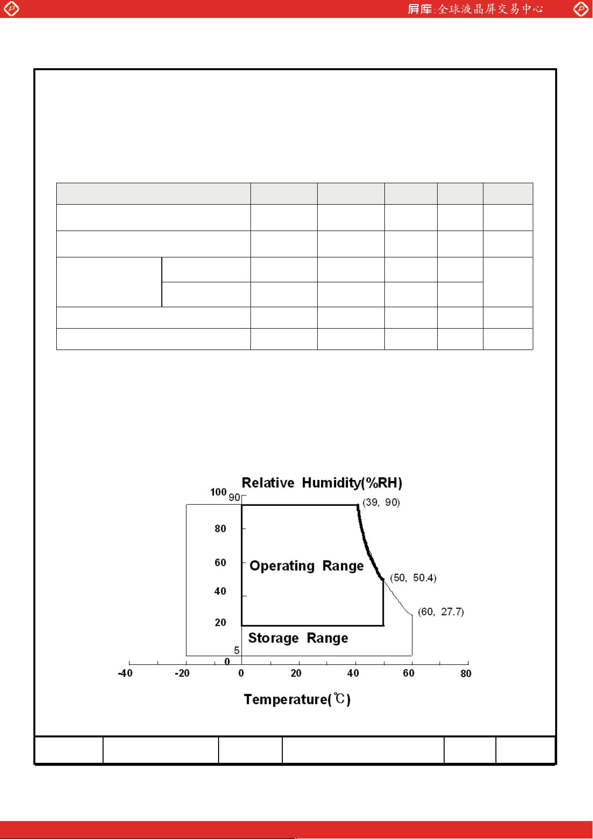
1. Absolute Maximum Ratings
If the condition exceeds maximum ratings, it can cause malfunction or unrecoverable
damage to the device.
www.panelook.com
NoteUnitMax.Min.SymbolItem
Power Supply Voltage
Storage temperature
Glass surface
Center
DD
STG
OPR
temperature
(Operation)
T. Uniformity
Shock ( non - operating )
Vibration ( non - operating )
Note (1) Ta= 25 • •2 ••C
(2) Temperature and relative humidity range are shown in the figure below.
a. 90 % RH Max. (Ta • •39 ••C)
b. Maximum wet-bulb temperature at 39 ••C or less. (Ta • •39 ••C)
c. No condensation
(3) 11ms, sine wave, one time for • •X, • •Y, • •Z axis
(4) 10-300 Hz, Sweep rate 10min, 30min for X,Y,Z axis
••T
nop
nop
60-20T
500T
10-
50
••
••
••
(1)V6.5GND-0.5V
(2)
(2),(5)
(3)G-S
(4)G1.5-V
Fig. Temperature and Relative humidity range
One step solution for LCD / PDP / OLED panel application: Datasheet, inventory and accessory!
www.panelook.com
Page 6
Global LCD Panel Exchange Center
• ••• • • • • • •• • • • • • • •• • • • • • • • • • • • • • • • • • • • • • • • • • • • • •• • • ••• • • • • • • • •• • • • • • • • • • • • • • • • • • • • • • • •• • • • • • • • • •
(5) Definition of test point
www.panelook.com
5mm
5mm
12
5
••
LCD Module (Active)
3
••
••T should be less than 10
T
: Temperature of the center of the glass surface (Test point 5)
OPR
(ƸT = | T
OPR–TMAX
T1~ T4 : Temperature of each edge of the glass surface
: The highest temperature of the glass surface
T
MAX
4
| )
One step solution for LCD / PDP / OLED panel application: Datasheet, inventory and accessory!
www.panelook.com
Page 7
Global LCD Panel Exchange Center
• ••• • • • • • •• • • • • • • •• • • • • • • • • • • • • • • • • • • • • • • • • • • • • •• • • ••• • • • • • • • •• • • • • • • • • • • • • • • • • • • • • • • •• • • • • • • • • •
2. Optical Characteristics
The optical characteristics should be measured in a dark room or equivalent.
Measuring equipment : TOPCON BM-7,SPECTRORADIOMETER SR-3
www.panelook.com
Contrast Ratio
(Center of screen)
Response
Time
Luminance of White
(Center of screen)
Color
Chromaticity
(CIE 1931)
Rising
Falling
Red
Green
Blue
White
(Ta = 25 • •2••C, VDD=5V, fv= 60Hz, f
TgG-to-G
L
Rx
Normal
TL,R=0
TU,D=0
Viewing
Angle
TYP.
-0.03
0.643
0.329Ry
0.286Gx
0.591Gy
0.144Bx
0.063By
0.280Wx
0.290Wy
=75MHz, IL= 6.0mArms)
DCLK
-1200800C/R
2116-Tr
129-Tf
msec
-8-
-450400Y
cd/m
2
TYP.
+0.03
NoteUnitMax.Typ.Min.ConditionSymbolItem
(3)
SR-3
(5)
BM-7
(6)
SR-3
(7),(8)
SR-3
-8975
-8975T
Degree
-8975T
-8975T
Viewing
Angle
Hor.
Ver.
T
L
R
U
D
C/R• •10
Brightness Uniformity
(9 Points)
uni
Note (1) Test Equipment Setup
The measurement should be executed in a stable, windless and dark room between
40min and 60min after lighting the back light at the given temperature for stabilization
of the back light. This should be measured in the center of screen.
Single lamp current : 6.0mA
Environment condition : Ta = 25 • •2 ••C
%-72--Color Gamut
K-10000--Color Temperature
(7)
SR-3
(7)
SR-3
(8)
SR-3
%25--B
(4)
SR-3
One step solution for LCD / PDP / OLED panel application: Datasheet, inventory and accessory!
www.panelook.com
Page 8
Global LCD Panel Exchange Center
• ••• • • • • • •• • • • • • • •• • • • • • • • • • • • • • • • • • • • • • • • • • • • • •• • • ••• • • • • • • • •• • • • • • • • • • • • • • • • • • • • • • • •• • • • • • • • • •
• •• •• •
• •
• •
• •
• • • •
• •
www.panelook.com
Field Photo detector
1• •SR-3
2• •BM-7
TFT - LCD Module
Note (2) Definition of test point
228 683 1138
Photo detector
Field
SR-3 : 50• •
BM-7 : 50• •
LCD Panel
The center of the screen
128
384
640
Note (3) Definition of Contrast Ratio (C/R)
: Ratio of gray max (Gmax) & gray min (Gmin) at the center point • •of the panel
CR
/
G
max
G
min
Gmax : Luminance with all pixels white
Gmin : Luminance with all pixels black
Active Area
Test Point
One step solution for LCD / PDP / OLED panel application: Datasheet, inventory and accessory!
www.panelook.com
Page 9
Global LCD Panel Exchange Center
• ••• • • • • • •• • • • • • • •• • • • • • • • • • • • • • • • • • • • • • • • • • • • • •• • • ••• • • • • • • • •• • • • • • • • • • • • • • • • • • • • • • • •• • • • • • • • • •
Note (4) Definition of 9 points brightness uniformity
www.panelook.com
BB
Buni
Bmax : Maximum brightness
Bmin : Minimum brightness
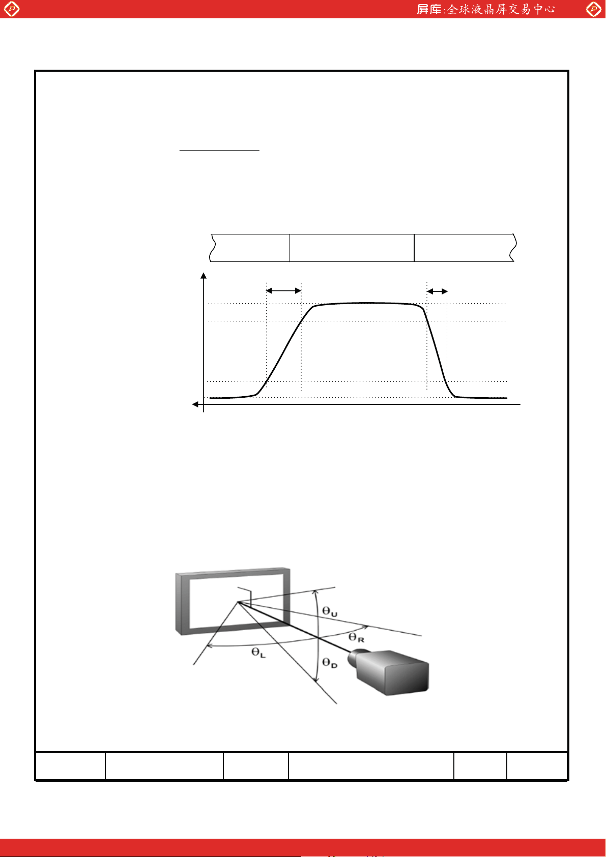
Note (5) Definition of Response time : Sum of Tr, Tf
Display data
Optical Instruments
Response
(max min)
100
100%
90%
10%
0%
B
max
Black (data off)
White (data on)
T
R
White (data off)
T
F
TIME
Note (6) Definition of Luminance of White : Luminance of white at center point • •
Note (7) Definition of Color Chromaticity (CIE 1931)
Color coordinate of Red, Green, Blue & White at center point • •
Note (8) Definition of Viewing Angle
: Viewing angle range (C/R ı10)
One step solution for LCD / PDP / OLED panel application: Datasheet, inventory and accessory!
www.panelook.com
Page 10

Global LCD Panel Exchange Center
• • ••• • • • • • • •• • • • • • • •• • • • • • • • • • • • • • • • • • • • • • • • • • • • • •• • • ••• • • • • • • • •• • • • • • • • • • • • • • • • • • • • • • • •• • • • • • • • • •
3. Electrical Characteristics
3.1 TFT LCD Module
The connector for display data & timing signal should be connected.
www.panelook.com
Ta = 25••C• •2••C
NoteUnitMax.Typ.Min.SymbolItem
Voltage of Power Supply
Current
(a) Black
of Power
DD
I
DD
Supply
Vsync Frequency
Hsync Frequency
Main Frequency
Rush Current
V
H
DCLK
RUSH
Note (1) The ripple voltage should be controlled under 10% of VDD.
V=60Hz, fDCLK = 75MHz, V
(2) f
= 5.0V, DC Current.
DD
(3) Power dissipation check pattern (LCD Module only)
a) Black Pattern b) White Pattern c) N-Pattern
(1)V5.55.04.5V
mA-750-
mA-1160-(b) White
(2),(3)
mA13901260-(c) N-Pattern
Hz-60-f
kHz534844f
MHz847565f
(4)A5--I
(4) Measurement Conditions
100%
90%
10%
GND
Rush Current I
can be measured when T
RUSH
T
RUSH
=470• •
. is 470• •.
RUSH
V
DD
One step solution for LCD / PDP / OLED panel application: Datasheet, inventory and accessory!
www.panelook.com
Page 11

Global LCD Panel Exchange Center
• • ••• • • • • • • •• • • • • • • •• • • • • • • • • • • • • • • • • • • • • • • • • • • • • •• • • ••• • • • • • • • •• • • • • • • • • • • • • • • • • • • • • • • •• • • • • • • • • •
www.panelook.com
3.2 Back Light Unit
The back light unit contains 6 U-type CCFTs ( Cold Cathode Fluorescent Tube ). The
characteristics of lamps are shown in the following tables.
Ta=25 • •2••C
NoteUnitMax.Typ.Min.SymbolItem
Lamp Current
Lamp Voltage
L
L
mArms5.0-4.0I
Vrms-1760-V
Note (1) It is defined as the time to take until the brightness reduces to 50% of its original value.
[Operating condition : Ta = 25• •2• •, IL = 6.0mArms(typ.), For single lamp only. ]
Inverter
Inverter
HOT 1
HOT 2
HOT 3
HOT 4
CCFT 1
CCFT 2
LCD
Module
HOT 11
HOT 12
CCFT 6
(1)Hour--50,000HrOperating Life Time
One step solution for LCD / PDP / OLED panel application: Datasheet, inventory and accessory!
www.panelook.com
Page 12

Global LCD Panel Exchange Center
• • ••• • • • • • • •• • • • • • • •• • • • • • • • • • • • • • • • • • • • • • • • • • • • • •• • • ••• • • • • • • • •• • • • • • • • • • • • • • • • • • • • • • • •• • • • • • • • • •
3.2.1 Inverter Input Condition & Specification
ConditionsSymbolItems
www.panelook.com
Specifications
NoteUnit
Max.Typ.Min.
Input
Voltage
Input
Current
Lamp
Current
Frequency
Backlight
On/Off
Dimming
Control
I
RUSH
LAMP
V
O
DIM
Vin=24.0V
Vdim=3.3V
Ta=25• • ••••••••V26.42421.6-Vin
Initial Turn-onA5--
mArms7.06.56.0Vdim=3.3 VI
kHz656055Vin=24.0 VF
-
-
5.25-2.4Vin=24.0 VON
-V
0.8-0Vin=24.0 VOFF
--3.3Max Lum
-V
0--Min. Lum
One step solution for LCD / PDP / OLED panel application: Datasheet, inventory and accessory!
www.panelook.com
Page 13

Global LCD Panel Exchange Center
• • ••• • • • • • • •• • • • • • • •• • • • • • • • • • • • • • • • • • • • • • • • • • • • • •• • • ••• • • • • • • • •• • • • • • • • • • • • • • • • • • • • • • • •• • • • • • • • • •
4. Block Diagram
www.panelook.com
One step solution for LCD / PDP / OLED panel application: Datasheet, inventory and accessory!
www.panelook.com
Page 14

Global LCD Panel Exchange Center
• • ••• • • • • • • •• • • • • • • •• • • • • • • • • • • • • • • • • • • • • • • • • • • • • •• • • ••• • • • • • • • •• • • • • • • • • • • • • • • • • • • • • • • •• • • • • • • • • •
5. Input Terminal Pin Assignment
5.1. Input Signal & Power Connector : FI-E30S (JAE)
www.panelook.com
DescriptionPIN No.DescriptionPIN No.
GND16No Connection1
RxIN3-17No Connection2
RxIN3+18No Connection3
GND19GND4
GND20RxIN0-5
LVDS OPTION (Note 1)21RxIN0+6
No Connection22GND7
GND23RxIN1-8
Note) No Connection: This PINS are only used for SAMSUNG internal using.
(1) LVDS OPTION : If this PIN : HIGH (3.3 V) or OPEN • • Normal LVDS format
: LOW (GND) • • JEIDA LVDS format
SEQUENCE : On = V
OFF = Interface Signal(T3) • •LVDS Option • •V
DD(T1) • •LVDS Option • •Interface Signal(T2)
DD
GND24RxIN1+9
GND25GND10
Vin26RxIN2-11
Vin27RxIN2+12
Vin28GND13
Vin29RxCLK-14
Vin30RxCLK+15
One step solution for LCD / PDP / OLED panel application: Datasheet, inventory and accessory!
www.panelook.com
Page 15

Global LCD Panel Exchange Center
• • ••• • • • • • • •• • • • • • • •• • • • • • • • • • • • • • • • • • • • • • • • • • • • • •• • • ••• • • • • • • • •• • • • • • • • • • • • • • • • • • • • • • • •• • • • • • • • • •
Note(1) Pin number starts from Right side
www.panelook.com
PCB
••
Pin No. 1 Pin No. 30
#1
connect name
#1
#30
#30
Fig. Connector diagram
a. All GND pins should be connected together and also be connected to the LCD’s
metal chassis.
b. All power input pins should be connected together.
c. All NC pins should be separated from other signal or power.
One step solution for LCD / PDP / OLED panel application: Datasheet, inventory and accessory!
www.panelook.com
Page 16

Global LCD Panel Exchange Center
• • ••• • • • • • • •• • • • • • • •• • • • • • • • • • • • • • • • • • • • • • • • • • • • • •• • • ••• • • • • • • • •• • • • • • • • • • • • • • • • • • • • • • • •• • • • • • • • • •
5.2. Inverter Input Pin Configuration
www.panelook.com
Connector : S14B-PH-SM3-TB(JST)
Pin Configuration(FUNCTION)Pin No.
24 V1
24 V2
24 V3
24 V4
24 V5
GND6
GND7
GND8
GND9
GND10
11
* ERROR DETECTION (NORMAL : GND / ABNORMAL : 5V)
Backlight On /Off [ON:2.4 - 5.25 V, OFF: 0 - 0.8 V]12
Dimming Control [0V:Min, 3.3V:Max]13
External PWM Signal - Note (1)14
No Connection
Note (1) When use Ext PWM Signal : Pin 13 must fix at 3.3V
When do not use Ext PWM Signal : Pin 14 must No Connection.
High-duty = On/(On+Off) * 100
On
Off
5.3. Inverter Input Power Sequence
0.95 Vin
Vin (24V)
Dimming Control
( 0 ~ 3.3 V )
20msec [Min]
0.1 Vin
1.1sec [Min]
On Off
0.5sec [Min]
0.5sec [Min]
Back Light On/Off
0.5sec [Min]
2.4 V
0.1sec [Min]
One step solution for LCD / PDP / OLED panel application: Datasheet, inventory and accessory!
www.panelook.com
Page 17

Global LCD Panel Exchange Center
• • ••• • • • • • • •• • • • • • • •• • • • • • • • • • • • • • • • • • • • • • • • • • • • • •• • • ••• • • • • • • • •• • • • • • • • • • • • • • • • • • • • • • • •• • • • • • • • • •
5.4 LVDS Interface
- LVDS Receiver : Tcon (merged)
- Data Format (JEIDA & Normal)
www.panelook.com
VESA -DATAJEIDA -DATALVDS pin
R0R2TxIN/RxOUT0
R1R3TxIN/RxOUT1
R2R4TxIN/RxOUT2
TxOUT/RxIN0
TxOUT/RxIN1
TxOUT/RxIN2
R3R5TxIN/RxOUT3
R4R6TxIN/RxOUT4
R5R7TxIN/RxOUT6
G0G2TxIN/RxOUT7
G1G3TxIN/RxOUT8
G2G4TxIN/RxOUT9
G3G5TxIN/RxOUT12
G4G6TxIN/RxOUT13
G5G7TxIN/RxOUT14
B0B2TxIN/RxOUT15
B1B3TxIN/RxOUT18
B2B4TxIN/RxOUT19
B3B5TxIN/RxOUT20
B4B6TxIN/RxOUT21
B5B7TxIN/RxOUT22
HSYNCHSYNCTxIN/RxOUT24
VSYNCVSYNCTxIN/RxOUT25
TxOUT/RxIN3
RESERVEDRESERVEDTxIN/RxOUT23
One step solution for LCD / PDP / OLED panel application: Datasheet, inventory and accessory!
DENDENTxIN/RxOUT26
R6R0TxIN/RxOUT27
R7R1TxIN/RxOUT5
G6G0TxIN/RxOUT10
G7G1TxIN/RxOUT11
B6B0TxIN/RxOUT16
B7B1TxIN/RxOUT17
www.panelook.com
Page 18
Global LCD Panel Exchange Center
• • ••• • • • • • • •• • • • • • • •• • • • • • • • • • • • • • • • • • • • • • • • • • • • • •• • • ••• • • • • • • • •• • • • • • • • • • • • • • • • • • • • • • • •• • • • • • • • • •
www.panelook.com
5.5 Input Signals, Basic Display Colors and Gray Scale of Each Color
COLOR
BASIC
COLOR
GRAY
SCALE
OF
RED
GRAY
SCALE
OF
GREEN
GRAY
SCALE
OF
BLUE
DISPLAY
(8bit)
BLACK
EN
ITE
DA
RK
••
••
LIGHT
D
RK
DA
••
••
LIGHT
EN
RK
DA
••
••
LIGHT
DATA SIGNAL
:::::::::
:::::::::::
BLUEGREENRED
1111111111111100000000CYAN
111111111111111111WH
:::::::::
::::::::::::::::::
00000000000011111111RE
:::::::
::::::::::::::::::
0000001111111100000000GRE
:::::::::::::
:::::
::::::::::::::::::
GRAY
SCALE
LEVEL
B7B6B5B4B3B2B1B0G7G6G5G4G3G2G1G0R7R6R5R4R3R2R1R0
-000000000000000000000000
-111111110000000000000000BLUE
-000000001111111100000000GRE
-11
-000000000000000011111111RED
-111111110000000011111111MAGENTA
-000000001111111111111111YELLOW
-111111
R0000000000000000000000000BLACK
R1000000000000000000000001
R2000000000000000000000010
R3~
R252
R252000000000000000011111101
R252000000000000000011111110
R2520000
G0000000000000000000000000BLACK
G1000000000000000100000000
G2000000000000001000000000
G3~
G252
G252000000001111110100000000
G252000000001111111000000000
G25200
B0000000000000000000000000BLACK
B1000000010000000000000000
B2000000100000000000000000
B3~
B252
B252111111010000000000000000
B252111111100000000000000000
B252111111110000000000000000BLUE
Note) Definition of Gray :
Rn : Red Gray, Gn : Green Gray, Bn : Blue Gray (n = Gray level)
Input Signal : 0 = Low level voltage, 1 = High level voltage
One step solution for LCD / PDP / OLED panel application: Datasheet, inventory and accessory!
www.panelook.com
Page 19

Global LCD Panel Exchange Center
• • ••• • • • • • • •• • • • • • • •• • • • • • • • • • • • • • • • • • • • • • • • • • • • • •• • • ••• • • • • • • • •• • • • • • • • • • • • • • • • • • • • • • • •• • • • • • • • • •
6. Interface Timing
6.1 Timing Parameters ( DE only mode )
www.panelook.com
NOTEUnitMAX.TYP.MIN.SYMBOLITEMSIGNAL
Clock
Hsync
Vsync
Frequency
C
H
V
Active
Vertical
Display
Period
VD
Display Term
Vertical
Total
VB
Active
Horizontal
Display
Period
HD
Display Term
Horizontal
Total
H
Note) This product is DE only mode. The input of Hsync & Vsync signal does
not have an effect on normal operation.
(1) Test Point : TTL control signal and CLK at LVDS Tx input terminal in system
(2) Internal VDD = 3.3V
-MHz8475651/T
-KHz534844F
-Hz-60-F
-lines-768-T
-Lines1000806773T
-clocks-1366-T
-clocks175016881420T
One step solution for LCD / PDP / OLED panel application: Datasheet, inventory and accessory!
www.panelook.com
Page 20

Global LCD Panel Exchange Center
• • ••• • • • • • • •• • • • • • • •• • • • • • • • • • • • • • • • • • • • • • • • • • • • • •• • • ••• • • • • • • • •• • • • • • • • • • • • • • • • • • • • • • • •• • • • • • • • • •
6.2 Timing diagrams of interface signal ( DE only mode )
www.panelook.com
TV
DE
DE
DCLK
DATA
SIGNALS
TVD
TVB
TH
THD
TC
DCLK
DISPLAY
DATA
DE
TC
TCH
TDS TDH
TES
TCL
0.5
V
0.5
V
CC
0.5
V
CC
CC
One step solution for LCD / PDP / OLED panel application: Datasheet, inventory and accessory!
www.panelook.com
Page 21

Global LCD Panel Exchange Center
• • ••• • • • • • • •• • • • • • • •• • • • • • • • • • • • • • • • • • • • • • • • • • • • • •• • • ••• • • • • • • • •• • • • • • • • • • • • • • • • • • • • • • • •• • • • • • • • • •
• •• •• • • • • •
6.3 Power ON/OFF Sequence
To prevent a latch-up or DC operation of the LCD Module, the power on/off
sequence should be as the diagram below.
0<T1• •10msec
0<T2• •50msec
0<T3• •50msec
1000msec• •T4
www.panelook.com
1000msec• •T5
(Recommend Value)
100msec• •T6
(Recommend Value)
T1 : VDDrising time from 10% to 90%
T2 : The time from V
T3 : The time from valid data off to V
T4 : V
off time for Windows restart
DD
to valid data at power ON.
DD
off at power Off.
DD
T5 : The time from valid data to B/L enable at power ON.
T6 : The time from valid data off to B/L disable at power Off.
The supply voltage of the external system for the Module input should be the same
as the definition of V
DD
.
Apply the lamp voltage within the LCD operation range. When the back light turns on
before the LCD operation or the LCD turns off before the back light turns off,
the display may momentarily show abnormal screen.
In case of V
= off level,
DD
please keep the level of input signals low or keep a high impedance.
T4 should be measured after the Module has been fully discharged between power off
and on period.
Interface signal should not be kept at high impedance when the power is on.
One step solution for LCD / PDP / OLED panel application: Datasheet, inventory and accessory!
www.panelook.com
Page 22

Global LCD Panel Exchange Center
www.panelook.com
One step solution for LCD / PDP / OLED panel application: Datasheet, inventory and accessory!
www.panelook.com
Page 23

Global LCD Panel Exchange Center
www.panelook.com
One step solution for LCD / PDP / OLED panel application: Datasheet, inventory and accessory!
www.panelook.com
Page 24

Global LCD Panel Exchange Center
• • ••• • • • • • • •• • • • • • • •• • • • • • • • • • • • • • • • • • • • • • • • • • • • • •• • • ••• • • • • • • • •• • • • • • • • • • • • • • • • • • • • • • • •• • • • • • • • • •
8. PACKING
8.1 CARTON (Internal Package)
(1) Packing Form
Corrugated fiberboard box and corrugated cardboard as shock absorber
(2) Packing Method
Packing Pallet Box
www.panelook.com
Cushion Set
8.2 Packing Specification
LCD Packing
Pallet
30 ea / (Packing-
Pallet Box)
122.3 kgTotal Pallet Weight
Module (15EA)
RemarkSpecificationItem
1. 90.0kg/LCD(30ea)
2. 14.8kg/Cushion Set(4ea)
4. 8.7kg/Packing-Pallet Box(1ea)
5. Cushion Material : EPS
6. Packing Pallet Box Material : DW4
Pallet weight : 8.8kg1 Box / PalletPallet
-VerticalPacking Direction
1265mm(H) x 1145mm(V) x 928mm(Height)H x V x heightTotal Pallet Size
Pallet(8.8kg) + Module(3*30=90kg) +
Cushion(14.8kg) + Pallet-BOX(8.7kg)
One step solution for LCD / PDP / OLED panel application: Datasheet, inventory and accessory!
www.panelook.com
Page 25

Global LCD Panel Exchange Center
• • ••• • • • • • • •• • • • • • • •• • • • • • • • • • • • • • • • • • • • • • • • • • • • • •• • • ••• • • • • • • • •• • • • • • • • • • • • • • • • • • • • • • • •• • • • • • • • • •
9. MARKING & OTHERS
A nameplate bearing followed by is affixed to a shipped product at the specified
location on each product.
(1) Parts number : LTA230W2-L01-XXXX
(2) Revision: One letters
(3) Lot number : X X X X XXX XX X
(4) Nameplate Indication
www.panelook.com
Cell Position No. (In the Glass)
Glass No. (In the one Lot)
Lot No. (Glass)
Month
Year (Note1)
Product code
Line
LTA230W2-L01
••••••••••••••••••••••••••
(5) Packing box attach
••••••• •••••••••••••••••
80mm
••••••••
••••
Week code : 05 29
week
year
40mm
Revision code
Lot number
100mm
Part number
Revision code
Box serial number
165mm
(6) Others
1. After service part
Lamps cannot be replaced because of the narrow bezel structure.
One step solution for LCD / PDP / OLED panel application: Datasheet, inventory and accessory!
www.panelook.com
Page 26

Global LCD Panel Exchange Center
• • ••• • • • • • • •• • • • • • • •• • • • • • • • • • • • • • • • • • • • • • • • • • • • • •• • • ••• • • • • • • • •• • • • • • • • • • • • • • • • • • • • • • • •• • • • • • • • • •
10. Inspection Criteria
When products are shipped, incoming inspection should be carried out with a
sampling inspection based on MIL-STD-105E level II by AQL 1.0%.
CHANGE CONTROL
Design of the product may be changed regarding the specifications, appearance, parts
used, circuits, etc. for product improvement. If a design change is judged to affect the
specifications of this product, supplier should inform customer of the change in advance.
QUALITY CONTROL
www.panelook.com
In the event of a product failure under normal operating conditions, a product trouble
or a functional disorder that can be deemed to be the responsibility of supplier, supplier
should repair the fault or replace the product free of charge within one year from
the product delivery date. However, supplier does not take responsibility for the product
quality in the case of modifications not specified by supplier.
MAINTENANCE
The specifications of the functions of maintenance parts may be partially changed
within the range which provides equivalent or better quality.
In principle, maintenance parts should be product units.
When stopping manufacturing this product, supplier should notify customer in advance.
HANDLING OF DOUBTFUL POINTS
Any doubt not stipulated in this specification is to be resolved by mutual agreement
between customer and supplier, and supplier should make efforts for improvement
in good faith.
One step solution for LCD / PDP / OLED panel application: Datasheet, inventory and accessory!
www.panelook.com
Page 27

Global LCD Panel Exchange Center
• • ••• • • • • • • •• • • • • • • •• • • • • • • • • • • • • • • • • • • • • • • • • • • • • •• • • ••• • • • • • • • •• • • • • • • • • • • • • • • • • • • • • • • •• • • • • • • • • •
11. General Precautions
11.1 Handling
(a) When the Module is assembled, it should be attached to the system firmly
using all mounting holes. Be careful not to twist and bend the Module.
(b) Because the inverter use high voltage, it should be disconnected from power
before it is assembled or disassembled.
(c) Refrain from strong mechanical shock and / or any force to the Module.
In addition to damage, this may cause improper operation or damage to the Module
and CCFT back light.
(d) Note that polarizers are very fragile and could be damage easily.
Do not press or scratch the surface harder than a HB pencil lead.
www.panelook.com
(e) Wipe off water droplets or oil immediately. If you leave the droplets for a long
time, staining or discoloration may occur.
(f) If the surface of the polarizer is dirty, clean it using absorbent cotton or soft cloth.
(g) Desirable cleaners are water, IPA(Isopropyl Alcohol) or Hexane.
Do not use Ketone type materials(ex. Acetone), Ethyl alcohol, Toluene, Ethyl acid
or Methyl chloride. It might permanent damage to the polarizer due to chemical
reaction.
(h) If the liquid crystal material leaks from the panel, it should be kept away
from the eyes or mouth . In case of contact with hands, legs or clothes, it must
be washed away with soap thoroughly.
(i) Protect the Module from static, or the CMOS Gate Array IC would be damaged.
(j) Use finger-stalls with soft gloves in order to keep display clean during the
incoming inspection and assembly process.
(k) Do not disassemble the Module.
(l) Do not pull or fold the lamp wire.
(m) Do not adjust the variable resistor located on the Module.
(n) Protection film for polarizer on the Module should be slowly peeled off just before use
so that the electrostatic charge can be minimized.
(o) Pins of I/F connector should not be touched directly with bare hands.
One step solution for LCD / PDP / OLED panel application: Datasheet, inventory and accessory!
www.panelook.com
Page 28

Global LCD Panel Exchange Center
• • ••• • • • • • • •• • • • • • • •• • • • • • • • • • • • • • • • • • • • • • • • • • • • • •• • • ••• • • • • • • • •• • • • • • • • • • • • • • • • • • • • • • • •• • • • • • • • • •
11.2 Storage
(a) Do not leave the Module in high temperature, and high humidity for a long time.
It is highly recommended to store the Module with temperature from 0 to 35• •
and relative humidity of less than 70%.
(b) Do not store the TFT-LCD Module in direct sunlight.
(c) The Module should be stored in a dark place. It is prohibited to apply sunlight or
fluorescent light in storing.
11.3 Operation
www.panelook.com
(a) No Connection or disconnect the Module in the "Power On" condition.
(b) Power supply should always be turned on/off by the "Power on/off sequence"
(c) Module has high frequency circuits. Sufficient suppression to the electromagnetic
interference should be done by system manufacturers. Grounding and shielding methods
may be important to minimize the interference.
(d) The cable between the back light connector and its inverter power supply should
be connected directly with a minimized length. A longer cable between
the back light and the inverter may cause lower luminance of lamp(CCFT) and
may require higher startup voltage(Vs).
11.4 Operation Condition Guide
(a) The LCD product should be operated under normal conditions.
Normal condition is defined as below;
- Temperature : 20• •15• •
- Humidity : 55• •20%
- Display pattern : continually changing pattern (Not stationary)
(b) If the product will be used in extreme conditions such as high temperature,
humidity, display patterns or operation time etc.., It is strongly recommended
to contact SEC for Application engineering advice. Otherwise, its reliability and
function may not be guaranteed. Extreme conditions are commonly found at
Airports, Transit Stations, Banks, Stock market, and Controlling systems.
One step solution for LCD / PDP / OLED panel application: Datasheet, inventory and accessory!
www.panelook.com
Page 29

Global LCD Panel Exchange Center
• • ••• • • • • • • •• • • • • • • •• • • • • • • • • • • • • • • • • • • • • • • • • • • • • •• • • ••• • • • • • • • •• • • • • • • • • • • • • • • • • • • • • • • •• • • • • • • • • •
11.5 Others
(a) Ultra-violet ray filter is necessary for outdoor operation.
(b) Avoid condensation of water. It may result in improper operation or disconnection
of electrode.
(c) Do not exceed the absolute maximum rating value. ( supply voltage variation,
input voltage variation, variation in part contents and environmental temperature,
and so on)
Otherwise the Module may be damaged.
(d) If the Module keeps displaying the same pattern for a long period of time,
the image may be "sticked" to the screen.
To avoid image sticking, it is recommended to use a screen saver.
www.panelook.com
(e) This Module has its circuitry PCB's on the rear side and should be handled
carefully in order not to be stressed.
(f) Please contact SEC in advance when you display the same pattern for a long time.
One step solution for LCD / PDP / OLED panel application: Datasheet, inventory and accessory!
www.panelook.com
 Loading...