

Page 1
SAMSUNG Confidential
MODEL
LSC320AN03
Doc. No
Page
1 / 23
SAMSUNG TFT-LCD
MODEL: LSC320AN03-W
The Information described in this specification is for the first draft and can be changed without prior notice
DATE: 11.Dec.2012
Samsung Display Co., LTD
Page 2
SAMSUNG Confidential
MODEL
LSC320AN03
Doc. No
Page
2 / 23
General Description
Description
This model uses a liquid crystal display (LCD) of amorphous silicon TFT as switching components. This
model is composed of a TFT LCD panel, a driver circuit, and an ass’y KIT of source PBA. This 46.0”
model has a resolution of a 1366 x 768 and can display up to 16.7 million colors with the wide viewing
angle of 89° or a higher degree in all directions. This panel is designed to support applications by
providing a excellent performance function of the flat panel display such as home-alone multimedia TFTLCD TV and a high definition TV.
General Information
Features
RoHS compliance (Pb-free)
High contrast ratio & aperture ratio with the wide color gamut
SPVA(Super patterned vertical align) mode
Wide viewing angle (±178°)
High speed response
HD resolution (16:9)
Low power consumption
DE (Data enable) mode
The interface (2pixel/clock) of 1ch LVDS (Low voltage differential signaling)
Items
Specification
Unit
Note
Active Display Area
697.6845 (H) x 392.256 (V)
㎜
Switching Components
a-Si TFT Active matrix
Glass Size
TFT : 713.0 (H) x 410.5 (V)
CF : 713.0 (H) x 408.2 (V)
mm
±0.4mm
Panel Size
713.0 (H) x 410.5 (V)
mm
±0.4mm
1.80(D)
mm
±0.1mm
Weight
1200 (max 1320)
g
± 10%
Display Colors
16.7M (True Display)
1.07B (Dithered 10bit)
color
Number of Pixels
1,366 × 768
pixel
16 : 9
Pixel Arrangement
RGB Vertical Stripe
Display Mode
Normally Black
Surface Treatment
AG-POL(Anti-Glare),
Haze
Haze 2.3%
± 2.1%
Hardness
Hard coating 2H
Page 3
SAMSUNG Confidential
MODEL
LSC320AN03
Doc. No
Page
3 / 23
1. Absolute Maximum Ratings
If the figures on measuring instruments exceed maximum ratings, it can cause the malfunction or the
unrecoverable damage on the device.
Item
Symbol
Min.
Max.
Unit
Note
Power supply voltage
V
DD
10.8
13.2
V
(1)
Temperature for storage
T
STG
-20
65
℃
(2),(4)
Temperature of glass surface
T
OPR2
0
65
℃
(2)
Operating temperature
T
OPR
0
50
℃
(2),(5)
Humidity for storage
H
STG
5
95
%RH
(2),(4)
Operating humidity
H
OPR
20
95
%RG
(2),(5)
Endurance on static electricity
150
V
(3)
Note (1) The power supply voltage at Ta= 25 ± 2 °C
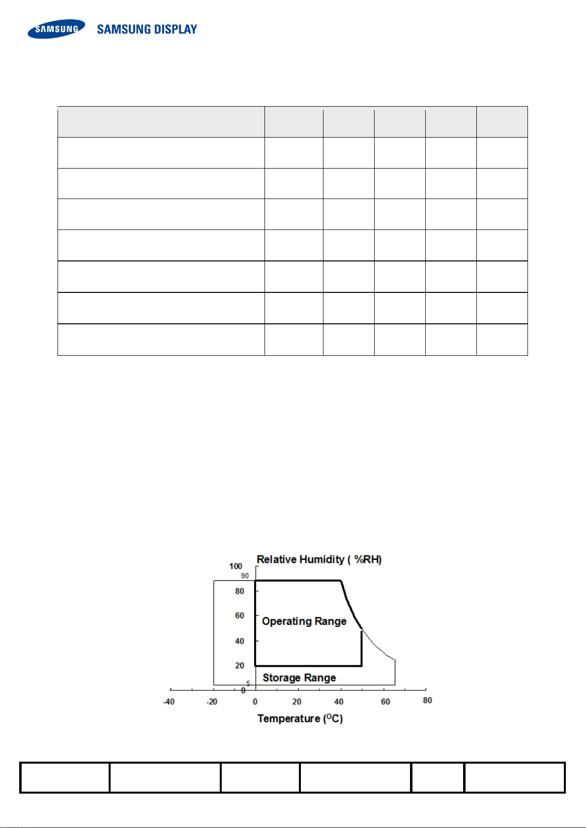
(2) Temperature and the range of relative humidity are shown in the figure below.
a. 95 % RH Max. (Ta ≤ 39 °C)
b. The relative humidity is 95% or less. (Ta >39 °C)
c. No condensation
d. Operating condition with SET
(3) Keep the static electricity under 150V in Polarizer attaching process.
(4) Operating condition with source PCB
(5) Storage temperature condition including glass
(6) Condition without packing. (Unpacking condition)
95
Fig. Range for temperature and relative humidity
Page 4
SAMSUNG Confidential
MODEL
LSC320AN03
Doc. No
Page
4 / 23
2. Optical characteristics
The optical characteristics should be measured in the dark room or the space surrounded by the similar setting.
Measuring equipment : TOPCON RD-80S, TOPCON SR-3 ,ELDIM EZ-Contrast
(Ta = 25 ± 2°C, VDD=12.0V, fv=60Hz, f
DCLK
=148.5MHz, Light source: D65 Standard light)
Item
Symbol
Condition
Min.
Typ.
Max.
Unit
Light Source
Note
Contrast ratio
(At the center of screen)
C/R
4000
5000
- Standard
(1)
SR-3
Response
time
G-to-G
Tg
T
PAN,SUR
=29.9℃
- 8 16
msec
Standard
or
VD BLU
(3)
RD-80S
Luminance of white
(At the center of screen)
YL
Normal
qL,R=0
qU,D=0
Viewing
Angle
250
300
-
cd/m2
VD BLU
(4)
SR-3
Chromaticity
(CIE 1931)
Red
Rx
TYP.
-0.03
0.640
TYP.
+0.03
VD BLU
(5),(6)
SR-3
Ry
0.330
Green
Gx
0.300
Gy
0.600
Blue
Bx
0.150
By
0.060
White
Wx
0.280
Wy
0.290
sRGB Concordance
-
99 %
(5)
SR-3
Color gamut
- - 72 - %
VD BLU
Color
- -
10,000 - K
Viewing
Angle
Hor.
qL
C/R≥10
75
89
-
Degree
Standard
or
VD BLU
(6)
SR-3
EZ-Contrast
qR
75
89
-
Ver.
qU
75
89
-
qD
75
89
-
Brightness uniformity
(9 Points)
B
uni
-
-
25
%
Standard
(2)
SR-3
Transmissivity
T 5.3
5.7 - %
Standard
(7)
D65/SR3
Transmissivity Uniformity
T
uni
- - 10 % Standard
(8)
D65/SR3
Gamma Value
GMA
(@20G~200G)
2.0
2.2
2.4
Standard
or
VD BLU
(9)
SR-3
Gamma variation
Gdiff
(@20G~128G)
-0.14 - 0.14
(11)
SR-3
ACC Linearity
ACC_lin
-0.015
-
0.015
Standard
or
VD BLU
(12)
SR-3
5nit Uniformity
Buni_5nit
-30 - 30
%
Standard
(38G/255G)
(10)
SR-3
White Color Coordinate
Uniformity
Wx uni
-
-
0.005
Standard
(13)
SR-3
Wy uni
0.008
Notice
Page 5
SAMSUNG Confidential
MODEL
LSC320AN03
Doc. No
Page
5 / 23
(a) Setup for test equipment
The measurement should be executed in a stable, windless, and dark room for 40min and 60min after
operating the panel at the given temperature for stabilization of the standard light. (SDC uses the standard
luminance of the D65 media).
This measurement should be measured at the center of screen.
The environment condition: Ta = 25 ± 2 °C
(b) D65 media has the general light source.
The temperature of color is 6847K. The coordinate of color is Wx 0.313, Wy 0.329
The luminance of this product is 7217cd/㎡.
Photo detector
Field
SR-3
2°/1°
RD-80S
1°
(c) The CIE positions D65 as the standard daylight illuminant:
[D65] is intended to represent average daylight and has a correlated color temperature of
approximately 6500 K. CIE standard illuminant D65 should be used in all colorimetric calculations
requiring representative daylight, unless there are specific reasons for using a different illuminant.
- Definition of the test point
Note (1) Definition of contrast ratio (C/R)
: The ratio of gray max (Gmax) & gray min (Gmin) at the center point ⑤ of the panel
The measurement goes in D65 Standard light source
Gmax : The luminance with all white pixels
C R
G
G
/
max
min
Page 6
SAMSUNG Confidential
MODEL
LSC320AN03
Doc. No
Page
6 / 23
Gmin : The luminance with all black pixels
Note (2) Definition of the brightness uniformity of 9 points (Test pattern : The full white)
The measurement shall be executed with the standard light source of D65 .
Bmax : The maximum brightness
Bmin : The minimum brightness
Note (3) Definition of the response time : Sum of Tr, Tf
※ G-to-G : Average response time between whole gray scale to whole gray scale.
The response time is the value that was measured after it was operated in Samsung's standard BLU for
one hour.( at room temperature)
Note (4) The definition of luminance of white: The luminance of white at the center point ⑤
The measurement shall be executed with the standard light source of D65.
Note (5) The definition of chromaticity (CIE 1931)
The color coordinate of red, green, blue and white at the center point ⑤
The measurement shall be executed with the standard light source of D65.
Note (6) Definition of viewing angle
: The range of viewing angle (C/R ≥10)
The measurement shall be executed with the standard light source of D65.
The response
Of optical instruments
Buni
B B
B
100
( max min)
max
Display data
Page 7
SAMSUNG Confidential
MODEL
LSC320AN03
Doc. No
Page
7 / 23
Tuni
= 100*
Gamma Value :
20 ~ 200Gray : 2.0 ~ 2.4 (Typ. 2.2)
Buni_5nit
= 100*
Bmax_5nit : The maximum brightness at 5nit Gray
Bmin_5nit : The minimum brightness at 5nit Gray
Vertical 1/6 Point
[Panel Measure Point]
Vertical 1/6 Point
Note (7) Definition of transmissivity
The measurement shall be executed with the standard light source of D65.
Note (8) Definition of the Transmissivity uniformity of 9 points (Test pattern: The full white)
The measurement shall be executed with the standard light source of D65.
Tmax : The maximum Transmissivity
Tmin : The minimum Transmissivity
Note (9) Management Criteria of Gamma Value
Note (10) 5nit Low Gray Uniformity
Page 8

SAMSUNG Confidential
MODEL
LSC320AN03
Doc. No
Page
8 / 23
255Gray Wx/Wy value basis (a module unit basis)
a. Color coordinate differences are less than 15/1,000 at
Any Point above 30Gray and 255Gray
b. When Wx/Wy coordinates reverse at 0Gray, it permits
an once intersection under, 30Gray
Wx, uni
= Wx max-Wx min
Wx max : The maximum Wx
Wx min : The minimum Wx
Wy, uni
= Wy max-Wy min
Wy max: The maximum Wy
Wy min: The minimum Wy
Note (11) Gamma Variation between Center and Left (or Right)
Gamma measured at 10cm point from the left & right side is more less than 0.1 than Gamma
measured at Center
(Gamma measured at 10cm of the P-4 & P-6 is more less than 0.1 than Gamma measured at P-5)
Note (12) Management Criteria of ACC Linearity
Note (13) White Color Coordinate Uniformity of 9 points (Test pattern: The full white)
Page 9

SAMSUNG Confidential
MODEL
LSC320AN03
Doc. No
Page
9 / 23
3. Electrical characteristics – Sony Model Attached Reference file
3.1 TFT LCD Module
The connector for the display data & timing signal should be connected.
Ta = 25°C ± 2 °C
Item
Symbol
Min.
Typ.
Max.
Unit
Note
Voltage of power supply
V
DD
10.8
12.0
13.2
V
(1)
Current
of power
supply
(a) Black
I
DD
-
326
700
mA
(2),(3)
(b) White
-
369
700
mA
(c) V_Stripe
-
595
1000
mA
Vsync frequency
f
V
48
60
66
Hz
Hsync frequency
f
H
44
48
53
kHz
Main frequency
Fdclk
72
78
85
MHz
Rush current
I
RUSH
-
-
2
A
(4)
Note (1) The ripple voltage should be controlled fewer than 10% of V
DD
(Typ.) voltage.
(2) fV=60Hz, fDCLK =148.5MHz, VDD = 12.0V, DC Current.
(3) Power dissipation check pattern (LCD Module only)
(4) Conditions for measurement
a) Black pattern b) White pattern c) V Stripe
The rush current, I
RUSH
can be measured during T
RUSH
is 470us
Page 10

MODEL
LSC320AN03
Doc. No
Page
10 / 23
4. Block diagram
SAMSUNG Confidential
Page 11

SAMSUNG Confidential
MODEL
LSC320AN03
Doc. No
Page
11 / 23
5. The Pin assignment in the input terminal
5.1. Input signal & power
connector : YOUNHO (30Pin,SMD-A)
No
Signal
REMARK
1
WPN
WPN
2
SCL
I2C interface
3
SDA
4
GND
GND
5
LV0_N
LVDS
6
LV0_P
7
GND
GND
8
LV1_N
negative LVDS differential data input (0)
9
LV1_P
positive LVDS differential data input (0)
10
GND
GND
11
LV2_N
negative LVDS differential data input (1)
12
LV2_P
positive LVDS differential data input (1)
13
GND
GND
14
LVCLK_N
negative LVDS differential data input (Clock)
15
LVCLK_P
positive LVDS differential data input (Clock)
16
GND
GND
17
LV3_N
negative LVDS differential data input (3)
18
LV3_P
positive LVDS differential data input (3)
19
GND
GND
20
AGING_ENI
AGING OPTION (Low: Active)
21
LVDS_SEL
LVDS OPTION (Low: JEIDA, High: VESA)
22
WPN
WPN
23
GND
GND
24
GND
25
N.C
26
VIN
Power Supply : +12V
27
VIN
28
VIN
29
VIN
30
VIN
Page 12

SAMSUNG Confidential
MODEL
LSC320AN03
Doc. No
Page
12 / 23
Note (1) Pin number which starts from the left side.
a. Power GND pins should be connected to the LCD’s metal chassis.
b. All power input pins should be connected together.
c. All NC pins should be separated from other signal or power.
Note(2) LVDS OPTION : IF THIS PIN : LOW (GND V)/ NC → JEIDA LVDS FORMAT
OTHERWISE : HIGH (3.3V) → NORMAL NS LVDS FORMAT
Note(3) AGING ENABLE PIN / IF THIS PIN GND → BIST MODE (ROLLING PATTERN IS OPERATED)
Fig . The diagram of connector
Page 13

SAMSUNG Confidential
MODEL
LSC320AN03
Doc. No
Page
13 / 23
5.2 LVDS Interface
- LVDS receiver : T-con (merged) ( 8Bit)
- Data format
LVDS pin
JEIDA -DATA
Normal-DATA
TxOUT/RxIN0
TxIN/RxOUT0
R2
R0
TxIN/RxOUT1
R3
R1
TxIN/RxOUT2
R4
R2
TxIN/RxOUT3
R5
R3
TxIN/RxOUT4
R6
R4
TxIN/RxOUT6
R7
R5
TxIN/RxOUT7
G2
G0
TxOUT/RxIN1
TxIN/RxOUT8
G3
G1
TxIN/RxOUT9
G4
G2
TxIN/RxOUT12
G5
G3
TxIN/RxOUT13
G6
G4
TxIN/RxOUT14
G7
G5
TxIN/RxOUT15
B2
B0
TxIN/RxOUT18
B3
B1
TxOUT/RxIN2
TxIN/RxOUT19
B4
B2
TxIN/RxOUT20
B5
B3
TxIN/RxOUT21
B6
B4
TxIN/RxOUT22
B7
B5
TxIN/RxOUT24
HSYNC
HSYNC
TxIN/RxOUT25
VSYNC
VSYNC
TxIN/RxOUT26
DEN
DE
TxOUT/RxIN3
TxIN/RxOUT27
R0
R6
TxIN/RxOUT5
R1
R7
TxIN/RxOUT10
G0
G6
TxIN/RxOUT11
G1
G7
TxIN/RxOUT16
B0
B6
TxIN/RxOUT17
B1
B7
TxIN/RxOUT23
RESERVED
RESERVED
Page 14

SAMSUNG Confidential
MODEL
LSC320AN03
Doc. No
Page
14 / 23
5.3 Input signals, basic display colors and the gray scale of each color. (8bit))
COLOR
DISPLAY
(8bit)
DATA SIGNAL
GRAY
SCALE
LEVEL
RED
GREEN
BLUE
R0
R1
R2
R3
R4
R5
R6
R7
G0
G1
G2
G3
G4
G5
G6
G7
B0
B1
B2
B3
B4
B5
B6
B7
BASIC
COLOR
BLACK
0
0
0
0
0
0
0
0
0
0
0
0
0
0
0
0
0
0
0
0
0
0
0
0
-
BLUE
0
0
0
0
0
0
0
0
0
0
0
0
0
0
0
0
1
1
1
1
1
1
1
1
-
GREEN
0
0
0
0
0
0
0
0
1
1
1
1
1
1
1
1
0
0
0
0
0
0
0
0
-
CYAN
0
0
0
0
0
0
0
0
1
1
1
1
1
1
1
1
1
1
1
1
1
1
1
1
-
RED
1
1
1
1
1
1
1
1
0
0
0
0
0
0
0
0
0
0
0
0
0
0
0
0
-
MAGENTA
1
1
1
1
1
1
1
1
0
0
0
0
0
0
0
0
1
1
1
1
1
1
1
1
-
YELLOW
1
1
1
1
1
1
1
1
1
1
1
1
1
1
1
1
0
0
0
0
0
0
0
0
-
WHITE
1
1
1
1
1
1
1
1
1
1
1
1
1
1
1
1
1
1
1
1
1
1
1
1
-
GRAY
SCALE
OF
RED
BLACK
0
0
0
0
0
0
0
0
0
0
0
0
0
0
0
0
0
0
0
0
0
0
0
0
R0
DARK
↑
↓
LIGHT
1
0
0
0
0
0
0
0
0
0
0
0
0
0
0
0
0
0
0
0
0
0
0
0
R1
0
1
0
0
0
0
0
0
0
0
0
0
0
0
0
0
0
0
0
0
0
0
0
0
R2
:
:
:
:
:
:
:
:
:
:
:
:
:
:
:
:
:
:
R3~
R252
:
:
:
:
:
:
:
:
:
:
:
:
:
:
:
:
:
:
1
0
1
1
1
1
1
1
0
0
0
0
0
0
0
0
0
0
0
0
0
0
0
0
R253
0
1
1
1
1
1
1
1
0
0
0
0
0
0
0
0
0
0
0
0
0
0
0
0
R254
RED
1
1
1
1
1
1
1
1
0
0
0
0
0
0
0
0
0
0
0
0
0
0
0
0
R255
GRAY
SCALE
OF
GREEN
BLACK
0
0
0
0
0
0
0
0
0
0
0
0
0
0
0
0
0
0
0
0
0
0
0
0
G0
DARK
↑
↓
LIGHT
0
0
0
0
0
0
0
0
1
0
0
0
0
0
0
0
0
0
0
0
0
0
0
0
G1
0
0
0
0
0
0
0
0
0
1
0
0
0
0
0
0
0
0
0
0
0
0
0
0
G2
:
:
:
:
:
:
:
:
:
:
:
:
:
:
:
:
:
:
G3~
G252
:
:
:
:
:
:
:
:
:
:
:
:
:
:
:
:
:
:
0
0
0
0
0
0
0
0
1
0
1
1
1
1
1
1
0
0
0
0
0
0
0
0
G253
0
0
0
0
0
0
0
0
0
1
1
1
1
1
1
1
0
0
0
0
0
0
0
0
G254
GREEN
0
0
0
0
0
0
0
0
1
1
1
1
1
1
1
1
0
0
0
0
0
0
0
0
G255
GRAY
SCALE
OF
BLUE
BLACK
0
0
0
0
0
0
0
0
0
0
0
0
0
0
0
0
0
0
0
0
0
0
0
0
B0
DARK
↑
↓
LIGHT
0
0
0
0
0
0
0
0
0
0
0
0
0
0
0
0
1
0
0
0
0
0
0
0
B1
0
0
0
0
0
0
0
0
0
0
0
0
0
0
0
0
0
1
0
0
0
0
0
0
B2
:
:
:
:
:
:
:
:
:
:
:
:
:
:
:
:
:
:
B3~
B252
:
:
:
:
:
:
:
:
:
:
:
:
:
:
:
:
:
:
0
0
0
0
0
0
0
0
0
0
0
0
0
0
0
0
1
0
1
1
1
1
1
1
B253
0
0
0
0
0
0
0
0
0
0
0
0
0
0
0
0
0
1
1
1
1
1
1
1
B254
BLUE
0
0
0
0
0
0
0
0
0
0
0
0
0
0
0
0
1
1
1
1
1
1
1
1
B255
Note) The definition of gray :
Rn : Red gray, Gn : Green gray, Bn : Blue gray (n = Gray level)
Input signal : 0 = Low level voltage, 1 = High level voltage
Page 15

SAMSUNG Confidential
MODEL
LSC320AN03
Doc. No
Page
15 / 23
5.4 LVDS receiver : T-con (merged) ( 8Bit)
- Data format
LVDS pin
JEIDA -DATA
Normal -DATA
TxOUT/RxIN0
TxIN/RxOUT0
R2
R0
TxIN/RxOUT1
R3
R1
TxIN/RxOUT2
R4
R2
TxIN/RxOUT3
R5
R3
TxIN/RxOUT4
R6
R4
TxIN/RxOUT6
R7
R5
TxIN/RxOUT7
G2
G0
TxOUT/RxIN1
TxIN/RxOUT8
G3
G1
TxIN/RxOUT9
G4
G2
TxIN/RxOUT12
G5
G3
TxIN/RxOUT13
G6
G4
TxIN/RxOUT14
G7
G5
TxIN/RxOUT15
B2
B0
TxIN/RxOUT18
B3
B1
TxOUT/RxIN2
TxIN/RxOUT19
B4
B2
TxIN/RxOUT20
B5
B3
TxIN/RxOUT21
B6
B4
TxIN/RxOUT22
B7
B5
TxIN/RxOUT24
HSYNC
HSYNC
TxIN/RxOUT25
VSYNC
VSYNC
TxIN/RxOUT26
DEN
DE
TxOUT/RxIN3
TxIN/RxOUT27
R0
R6
TxIN/RxOUT5
R1
R7
TxIN/RxOUT10
G0
G6
TxIN/RxOUT11
G1
G7
TxIN/RxOUT16
B0
B6
TxIN/RxOUT17
B1
B7
TxIN/RxOUT23
RESERVED
RESERVED
TxOUT/RxIN4(dithered10b
it)
TxIN/RxOUT28
R0
R8
TxIN/RxOUT29
R1
R9
TxIN/RxOUT30
G0
G8
TxIN/RxOUT31
G1
G9
TxIN/RxOUT32
B0
B8
TxIN/RxOUT33
B1
B9
TxIN/RxOUT34
RESERVED
RESERVED
Page 16

SAMSUNG Confidential
MODEL
LSC320AN03
Doc. No
Page
16 / 23
5.5 Input signals, basic display colors and the gray scale of each color. (10bit)
COLOR
DISPLAY
DATA SIGNAL
GRAY
SCALE
LEVEL
RED
GREEN
BLUE
R0
R1
R2
R3
R4
R5
R6
R7
R8
R9
G0
G1
G2
G3
G4
G5
G6
G7
G8
G9
B0
B1
B2
B3
B4
B5
B6
B7
B8
B9
BASIC
COLOR
BLACK
0 0 0 0 0 0 0 0 0 0 0 0 0 0 0 0 0 0 0 0 0 0 0 0 0 0 0 0 0 0 -
BLUE
0 0 0 0 0 0 0 0 0 0 0 0 0 0 0 0 0 0 0 0 1 1 1 1 1 1 1 1 1 1 -
GREEN
0 0 0 0 0 0 0 0 0 0 1 1 1 1 1 1 1 1 1 1 0 0 0 0 0 0 0 0 0 0 -
CYAN
0 0 0 0 0 0 0 0 0 0 1 1 1 1 1 1 1 1 1 1 1 1 1 1 1 1 1 1 1 1 -
RED
1 1 1 1 1 1 1 1 1 1 0 0 0 0 0 0 0 0 0 0 0 0 0 0 0 0 0 0 0 0 -
MAGENTA
1 1 1 1 1 1 1 1 1 1 0 0 0 0 0 0 0 0 0 0 1 1 1 1 1 1 1 1 1 1 -
YELLOW
1 1 1 1 1 1 1 1 1 1 1 1 1 1 1 1 1 1 1 1 0 0 0 0 0 0 0 0 0 0 -
WHITE
1 1 1 1 1 1 1 1 1 1 1 1 1 1 1 1 1 1 1 1 1 1 1 1 1 1 1 1 1 1 -
GRAY
SCALE
OF RED
BLACK
0 0 0 0 0 0 0 0 0 0 0 0 0 0 0 0 0 0 0 0 0 0 0 0 0 0 0 0 0 0 R0
DARK
↑
↓
LIGHT
1 0 0 0 0 0 0 0 0 0 0 0 0 0 0 0 0 0 0 0 0 0 0 0 0 0 0 0 0 0 R1
0 1 0 0 0 0 0 0 0 0 0 0 0 0 0 0 0 0 0 0 0 0 0 0 0 0 0 0 0 0 R2
: : : : : : : : : : : : : : : : : : : : : : : : : : : : :
:
R3~
R1020
: : : : : : : : : : : : : : : : : : : : : : : : : : : : :
:
1 0 1 1 1 1 1 1 1 1 0 0 0 0 0 0 0 0 0 0 0 0 0 0 0 0 0 0 0 0 R1021
0 1 1 1 1 1 1 1 1 1 0 0 0 0 0 0 0 0 0 0 0 0 0 0 0 0 0 0 0 0 R1022
RED
1 1 1 1 1 1 1 1 1 1 0 0 0 0 0 0 0 0 0 0 0 0 0 0 0 0 0 0 0 0 R1023
GRAY
SCALE
OF
GREEN
BLACK
0 0 0 0 0 0 0 0 0 0 0 0 0 0 0 0 0 0 0 0 0 0 0 0 0 0 0 0 0 0 G0
DARK
↑
↓
LIGHT
0 0 0 0 0 0 0 0 0 0 1 0 0 0 0 0 0 0 0 0 0 0 0 0 0 0 0 0 0 0 G1
0 0 0 0 0 0 0 0 0 0 0 1 0 0 0 0 0 0 0 0 0 0 0 0 0 0 0 0 0 0 G2
: : : : : : : : : : : : : : : : : : : : : : : : : : : : :
:
G3~
G1020
: : : : : : : : : : : : : : : : : : : : : : : : : : : : : : 0 0 0 0 0 0 0 0 0 0 1 0 1 1 1 1 1 1 1 1 0 0 0 0 0 0 0 0 0 0 G1021
0 0 0 0 0 0 0 0 0 0 0 1 1 1 1 1 1 1 1 1 0 0 0 0 0 0 0 0 0 0 G1022
GREEN
0 0 0 0 0 0 0 0 0 0 1 1 1 1 1 1 1 1 1 1 0 0 0 0 0 0 0 0 0 0 G1023
GRAY
SCALE
OF
BLUE
BLACK
0 0 0 0 0 0 0 0 0 0 0 0 0 0 0 0 0 0 0 0 0 0 0 0 0 0 0 0 0 0 B0
DARK
↑
↓
LIGHT
0 0 0 0 0 0 0 0 0 0 0 0 0 0 0 0 0 0 0 0 1 0 0 0 0 0 0 0 0 0 B1
0 0 0 0 0 0 0 0 0 0 0 0 0 0 0 0 0 0 0 0 0 1 0 0 0 0 0 0 0 0 B2
: : : : : : : : : : : : : : : : : : : : : : : : : : : : :
:
B3~
B1020
: : : : : : : : : : : : : : : : : : : : : : : : : : : : :
:
0 0 0 0 0 0 0 0 0 0 0 0 0 0 0 0 0 0 0 0 1 0 1 1 1 1 1 1 1 1 B1021
0 0 0 0 0 0 0 0 0 0 0 0 0 0 0 0 0 0 0 0 0 1 1 1 1 1 1 1 1 1 B1022
BLUE
0 0 0 0 0 0 0 0 0 0 0 0 0 0 0 0 0 0 0 0 1 1 1 1 1 1 1 1 1 1 B1023
Note) The definition of gray :
Rn : Red gray, Gn : Green gray, Bn : Blue gray (n = Gray level)
Input signal : 0 = Low level voltage, 1 = High level voltage
Page 17

SAMSUNG Confidential
MODEL
LSC320AN03
Doc. No
Page
17 / 23
6. Interface timing
6.1 The parameters of timing ( Only DE mode )
SIGNAL
ITEM
SMBOL
MIN.
TYP.
MAX.
Unit
NOTE
Clock
Frequency
1/T
C
72
78
85
MHz
-
Hsync
F
H
44
48
53
KHz
-
Vsync
F
V
48
60
66
Hz
-
Term for the
vertical
display
Active
display
period
T
VD
-
768
-
Lines
-
Total vertical
T
V
780
802
1200
Lines
-
Term for the
horizontal
display
Active
display
period
T
HD
-
1368
-
Clocks
-
Total
Horizontal
T
H
1480
1624
2000
clocks
-
Note) These products don’t have to receive the signal of Hsync & Vsync from the input device.
(1) Key points when testing: TTL controls the signal and the CLK at the input terminal of LVDS Tx of the
system.
(2) Internal VDD = 3.3V
(3) Spread spectrum
- The limit of spread spectrum's range of SET in which the LCD module is assembled should be within ± 3 %.
TxOUT/RxIN4(dithered10bit)
TxIN/RxOUT28
R0
R8
TxIN/RxOUT29
R1
R9
TxIN/RxOUT30
G0
G8
TxIN/RxOUT31
G1
G9
TxIN/RxOUT32
B0
B8
TxIN/RxOUT33
B1
B9
TxIN/RxOUT34
RESERVED
RESERVED
Page 18

SAMSUNG Confidential
MODEL
LSC320AN03
Doc. No
Page
18 / 23
6.2 Timing diagrams of interface signal (Only DE mode )
Page 19

SAMSUNG Confidential
MODEL
LSC320AN03
Doc. No
Page
19 / 23
6.3 Characteristics of Input data of LVDS
ITEM
SYMBOL
Min.
Typ.
Max.
UNIT
NOTE
Differential input high
threshold voltage
VTH
-
-
+100
mV
V
CM
= 1.2V
Differential input low
threshold voltage
VTL
-100 - -
mV
Input common mode voltage
V
CM
0.2
1.2
2.0 V -
Differential Input Voltage
|V
ID
|
100
-
600
mV
|V
ID
|=100mV
Input data position
F
IN
=78MHz
t
RSRM
- - 450
ps
t
RSLM
-450
-
ps
Notice The spread spectrum should be 0% when the skew is measured.
Position of a measurement is T-CON LVDS input pin
Page 20

SAMSUNG Confidential
MODEL
LSC320AN03
Doc. No
Page
20 / 23
6.4 The sequence of power on and off
To prevent a latch-up phenomena or the DC operation of the LCD Module, the power on/off sequence should
be accorded with the settings described in the diagram below.
T1 : The VDD rising time from 10% to 90%
T2 : The time from the point which V
DD
reach to 90% of voltage to the point which the valid data is out when
the power is on.
T3: The time from the point which the valid data is out to the point which VDD reach to the 90% of voltage
when the power is off.
T4: the time from the point which the Vdd decrease to the point which the Vdd increase again for windows to
restart.
※ The recommended operating condition of the back light system
T5: The time which takes for B/L to be turned on after the signal is entered when the time is on.
T6 : The time which takes until the signal is out after BL is turned off
The condition of supply voltage to enter in the module from the external system should have
the same condition as the definition of VDD.
Apply the voltage for the lamp within the range which the LCD operates. when the back light is turned on
before the LCD is operated or when the LCD is turned off before the back light is turned off, the display may
show the abnormal screen momentarily.
While the V
DD
is off level, please keep the level of input signals low or keep a high impedance condition.
The figure of T4 should be measured after the module has been fully discharged between the periods
when the power is on and off.
The interface signal must not keep the high impedance condition when the power is on.
Page 21

SAMSUNG Confidential
MODEL
LSC320AN03
Doc. No
Page
21 / 23
7. Outline dimension
7.1 The adhesive size of POL
The next figure shows the size of POL on the drawing sheet attached to the panel for BLU design.
<Figure.>
The POL size of CF : 710.7 X 405.6 ± 0.5mm
The POL size of TFT: 710.7 X 405.6 ± 0.5mm
The total adhesion allowance of POL is ± 1.15㎜
7.2 The drawing sheet for the size of the OLB bonding
Page 22

MODEL
LSC320AN03
Doc. No
Page
22 / 23
8. Reliability test
8.1 Panel
Item
Test Condition
Quantity
Note
HTOL
60 ℃ (Panel change 500hr / circuit change 250hr)
8
LTOL
-5 ℃ (Panel change 500hr / circuit change 250hr)
4
THB
50 ℃ / 90 %RH(Panel change 500hr / circuit change 250hr)
10
ASG
Low
temperature
Max. frequency 25℃~-40℃
Each
Cell
ASG Product Only
ASG
High
Temperature
Min. frequency 60℃operation 96hr
Each
Cell
ASG Product Only
Image sticking
25 ℃ / Mosaic pattern(9*10) 12hrs
8
Rolling pattern 12hrs / 3cycles
Decompressio
n
-40~50℃, 0m(0ft) ~ 13,700m(45,000ft), 72.5Hr
4
HTS
70 ℃, Storage (Panel change 500hr / circuit change 250hr)
4
LTS
-25 ℃, Storage(Panel change 500hr / circuit change 250hr)
4
Transportation
condition
drop(20cm) → temperature/humidity(-30~60℃ / 40℃ 90%RH)
→ pressure → vibration(5~200Hz 1.05Grms, 2hr) → drop(20cm)
1pallet
WHTS
60 ℃ / 75 %RH , Storage
4
Noise
Electromagnetic noise: Overall 23dB 이하
2
Complex
stress
-20℃~60℃, 0~90%RH, 2cycle
4
ESD
S-IC Input ±7KV, Output ±4KV
Output 은 data TP 에 직접 인가 후 진행
Input 은 CKV,VCOM 등에 FFC CNT 를 통하여 TEST 를 진행
3
EOS (optional)
Item
Test condition
Vin Input
step
Surge combination (High impedance)
Pass Condition: 5kV under
Signal Input
step
Surge combination (High impedance)
Pass Condition: 120V under
2
[ Criteria on evaluation]
There should be no change of the product, which may affect to the practical display functions, when the
display quality test is executed under the normal operation setting.
* HTOL/ LTOL : The operating cycle on the high and low temperature
* THB : Temperature humidity slant
* HTS/LTS : The storage at the high and low temperature
* WHTS : The storage in the high temperature with the high humidity
SAMSUNG Confidential
Page 23

MODEL
LSC320AN03
Doc. No
Page
23 / 23
SAMSUNG Confidential
 Loading...