

SAMSUNG LSC320AN02-T Specification
Product Specification
( √ ) Preliminary Specification
( ) Approval Specification
Any Modification of Spec is not allowed without SDC’s permission
CUSTOMER Videocon
MODEL NO. LSC320AN02
DATE OF ISSUE 2012.12.28 EXTENSION CODE T
LCD Sales & Marketing Team
Samsung Display Co., Ltd
————————————————————————————————————————————————–
Table of Contents
REVISION HISTORY .................................................................................................................................................
1. GENERAL DESCRIPTION .....................................................................................................................................
2. ABSOLUTE MAXIMUM RATINGS .....................................................................................................................
3. OPTICAL CHARACTERISTICS .............................................................................................................................
4. ELECTRICAL CHARACTERISTICS........................................................................................................................
4.1 TFT LCD MODULE .......................................................................................................................................................
5. INPUT TERMINAL PIN ASSIGNMENT ..............................................................................................................
5.1 INPUT SIGNAL & POWER ...........................................................................................................................................
5.2 LVDS INTERFACE .........................................................................................................................................................
5.3 INPUT COLOR DATA MAPPING.................................................................................................................................
6. INTERFACE TIMING ............................................................................................................................................
6.1 TIMING PARAMETERS OF TIMING (ONLY DE MODE) ................................................................................................
6.2 TIMING DIAGRAMS OF INTERFACE SIGNAL ............................................................................................................
6.3 CHARACTREISTICS OF INPUT DATA OF LVDS .........................................................................................................
6.4 POWER ON/OFF SEQUENCE .....................................................................................................................................
7. OUTLINE DIMENSION ........................................................................................................................................
8. PACKING ..............................................................................................................................................................
8.1 CARTON ..............................................................................................................................................................
8.2 MARKING ............................................................................................................................................................
9. GENERAL PRECAUTIONS ...................................................................................................................................
9.1 HANDLING ..................................................................................................................................................................
9.2 STORAGE .....................................................................................................................................................................
9.3 OPERATION .................................................................................................................................................................
9.4 OPERATION CONDITION GUIDE................................................................ ................................ ...............................
9.5 OTHERS ........................................................................................................................................................................
——————————————————————————————————————————————––—
Doc.No. LSC320AN02 Page 2 of 36 Rev.No. 06-000-G-20121228
————————————————————————————————————————————————–
REVISION HISTORY
Date. Rev.No. Page Revision Description
2012.12.28 000 Initial Release
——————————————————————————————————————————————––—
Doc.No. LSC320AN02 Page 3 of 36 Rev.No. 06-000-G-20121228
————————————————————————————————————————————————–
1. GENERAL DESCRIPTION
DESCRIPTION
This model uses a liquid crystal display (LCD) of amorphous silicon TFT as switching components. This model is
composed of a TFT LCD panel, a driver circuit, and an ass’y KIT of source PBA. This 32.0” model has a
resolution of a 1366 x 768 and can display up to 16.7 million colors with the wide viewing angle of 89° or a
higher degree in all directions. This panel is designed to support applications by providing a excellent
performance function of the flat panel display such as home-alone multimedia TFT-LCD TV and a high
definition TV.
FEATURES
RoHS compliance (Pb-free)
High contrast ratio & aperture ratio with the wide color gamut
PVA(Patterned vertical align) mode
Wide viewing angle (± 178°)
High speed response
HD resolution (16:9)
DE (Data enable) mode
The interface (1Pixel/clock) of LVDS (Low voltage differential signaling)
GENERAL INFORMATION
Item Specification Unit Note
Active Display Area
Switching Components
Glass size
Panel Size
Weight
Display Colors
Number of Pixels
Pixel Arrangement
Display Mode
Haze
Hardness
697.6845 (H) x 392.256 (V)
a-Si TFT Active matrix
TFT : 713.0(H) x 410.50(V)
CF : 713.0(H) x 408.20(V)
713.0(H) x 410.5(V)
1.80(D)
1200 (Max)
16.7M (True 8-bit)
1,366 × 768
RGB Horizontal Stripe
Normally Black
2%
Hard coating 2H
mm
mm
mm 16:9
mm
g
mm
——————————————————————————————————————————————––—
Doc.No. LSC320AN02 Page 4 of 36 Rev.No. 06-000-G-20121228
————————————————————————————————————————————————–
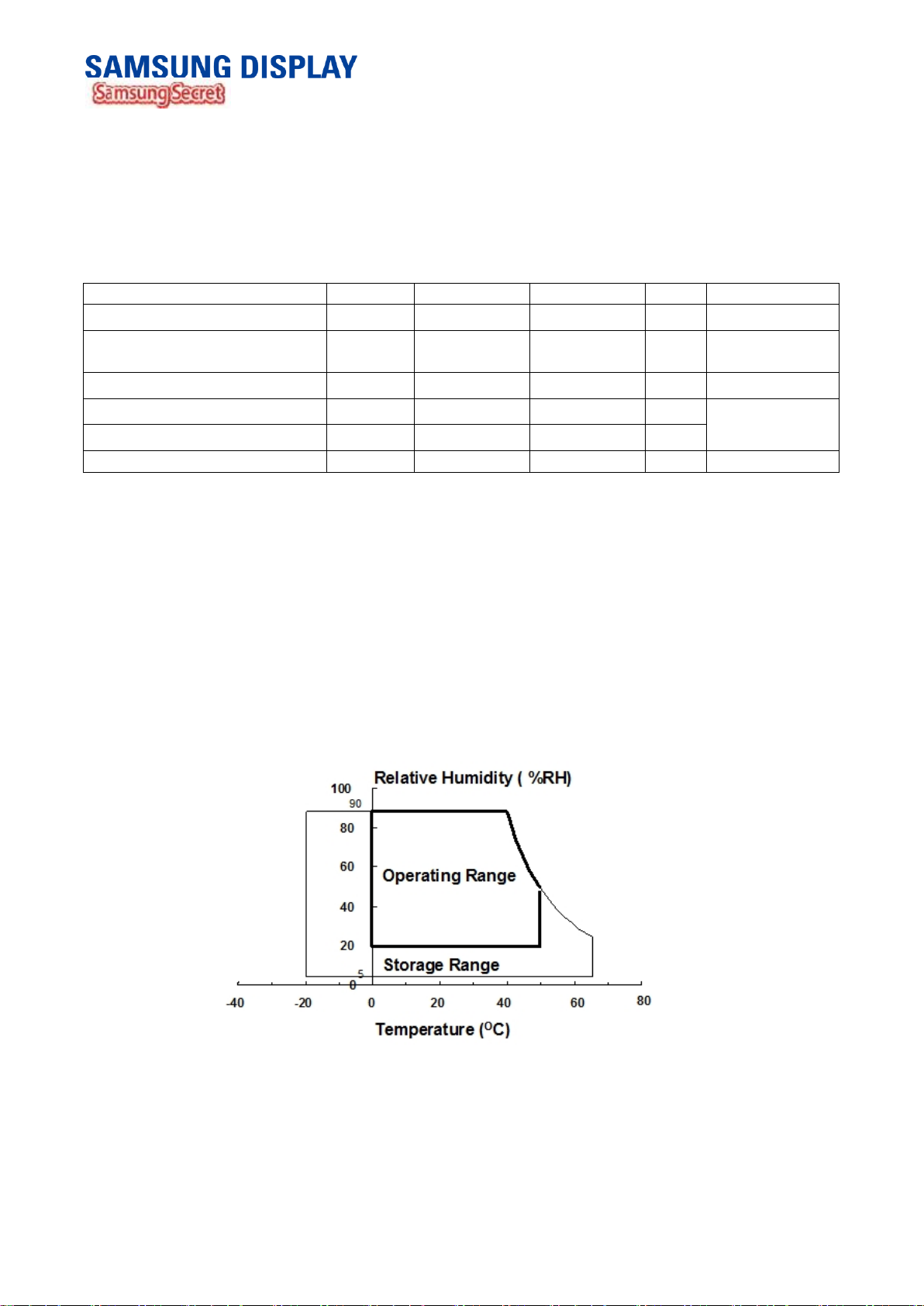
2. ABSOLUTE MAXIMUM RATINGS
If the figures on measuring instruments exceed maximum ratings, it can cause the malfunction or the
unrecoverable damage on the device.
Item Symbol Min. Max. Unit Note
Power supply voltage VDD
Temperature for storage
(Temperature of glass surface)
Humidity for storage H
Operating temperature T
Operating humidity H
T
STG
STG
OPR
STG
Endurance on static electricity 150 V (3)
Note (1) The power supply voltage at Ta= 25 ± 2 °C
(2) Temperature and the range of relative humidity are shown in the figure below.
a. 90 % RH Max. (Ta ≤ 39 °C)
GND-0.5 14.0 V (1)
-20 65 C (2), (4)
5 90 %RH (2), (4)
0 50 C
20 90 %RH
(2), (5)
b. The relative humidity is 90% or less. (Ta >39 °C)
c. No condensation
(3) Keep the static electricity under 150V in Polarizer attaching process.
(4) Operating condition with source PCB
(5) Storage temperature condition including glass
(6) Condition without packing. (Unpacking condition)
Fig. Range for temperature and relative humidity (unpacking condition)
——————————————————————————————————————————————––—
Doc.No. LSC320AN02 Page 5 of 36 Rev.No. 06-000-G-20121228
————————————————————————————————————————————————–
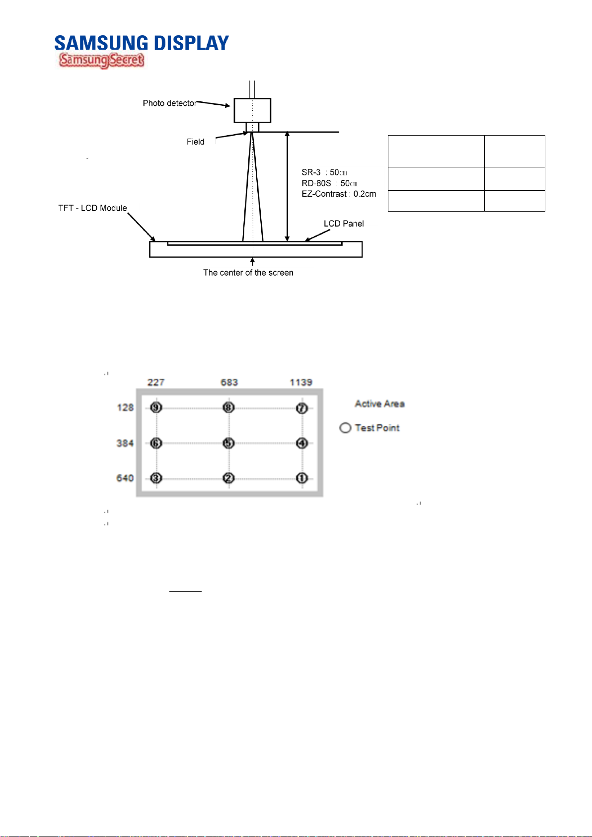
3. OPTICAL CHARACTERISTICS
The optical characteristics should be measured in the dark room or the space surrounded by the similar
setting. Measuring equipment : TOPCON RD-80S, TOPCON SR-3 ,ELDIM EZ-Contrast
Ta = 25 ± 2°C, VDD=12.0V, fv=60Hz, fDCLK=78MHz, Light source: D65
Item Symbol Condition Min. Typ. Max. Unit Note
Contrast Ratio CR
Response time G-to-G
Luminance of white
(At the center of screen))
Red
Color
Green
Chromaticity
(CIE)
Blue
White
Viewing
Angle
Hor.
Ver.
Tg
YL
RX
RY
GX 0.269
GY 0.583
`Normal
qL,R=0
qU,D=0
Viewing
Angle
BX 0.135
BY 0.117
WX 0.297
WY 0.361
q
q
q
q
CR 10
At center
3000 5000 - -
- 20 30 msec
440 480
- cd/m2
0.660
0.329
TYP
-0.03
79 89
79 89
79 89
79 89
TYP
+0.03
-
-
-
-
Degrees
Color Gamut - 68 - %
Color - 7000 - K
Notice
(a) Setup for test equipment
The measurement should be executed in a stable, windless, and dark room for 40min and 60min after
operating the panel at the given temperature for stabilization of the standard light. (SDC uses the standard
luminance of the D65media).
This measurement should be measured at the center of screen.
The environment condition: Ta = 25 ± 2 °C
(b) D65media has the general light source.
The temperature of color is 6487K. The coordinate of color is Wx 0.313, Wy 0.329
The luminance of this product is 7217cd/㎡.
(1)
SR-3
(2)
RD-80S
(3)
SR-3
(4),(5)
SR-3
(5)
SR-3
EZ-Contrast
——————————————————————————————————————————————––—
Doc.No. LSC320AN02 Page 6 of 36 Rev.No. 06-000-G-20121228
————————————————————————————————————————————————–
(c)
The CIE positions D65 as the standard daylight illuminant:
[D65] is intended to represent average daylight and has a correlated color temperature of approximately 6500
K. CIE standard illuminant D65 should be used in all colorimetric calculations requiring representative daylight,
unless there are specific reasons for using a different illuminant.
- Definition of the test point
Photo detector Field
SR-3 2°
RD-80S 1°
Note (1) Definition of contrast ratio (C/R)
: The ratio of gray max (Gmax) & gray min (Gmin) at the center point ⑤ of the panel
The measurement goes in ELABO-LS Standard light source
——————————————————————————————————————————————––—
C R
Gmax : The luminance with all white pixels
Gmin : The luminance with all black pixels
G
/
max
G
min
Doc.No. LSC320AN02 Page 7 of 36 Rev.No. 06-000-G-20121228
————————————————————————————————————————————————–
Note (2) Definition of response time
Display data
The response of
optical instruments
※ G-to-G : Average response time between the whole gray scale to the whole gray scale.
Gray to Gray Response Time
End
Ton
Toff
Start
Gray
0
31
63
95
127
159
191
223
255
0 31 63 95 127 159 191 223 255
Tr(0-31) Tr(0-63) Tr(0-95) Tr(0-127) Tr(0-159) Tr(0-191) Tr(0-223) Tr(0-255)
Tf(31-0) Tr(31-63) Tr(31-95) Tr(31-127) Tr(31-159) Tr(31-191) Tr(31-223) Tr(31-255)
Tf(63-0) Tf(63-31) Tr(63-95) Tr(63-127) Tr(63-159) Tr(63-191) Tr(63-223) Tr(63-255)
Tf(95-0) Tf(95-31) Tf(95-63) Tr(95-127) Tr(95-159) Tr(95-191) Tr(95-223) Tr(95-255)
Tf(127-0) Tf(127-31) Tf(127-63) Tf(127-95) Tr(127-159) Tr(127-191) Tr(127-223) Tr(127-255)
Tf(159-0) Tf(159-31) Tf(159-63) Tf(159-95) Tf(159-127) Tr(159-191) Tr(159-223) Tr(159-255)
Tf(191-0) Tf(191-31) Tf(191-63) Tf(191-95) Tf(191-127) Tf(191-159) Tr(191-223) Tr(191-255)
Tf(223-0) Tf(223-31) Tf(223-63) Tf(223-95) Tf(223-127) Tf(223-159) Tf(223-191) Tr(223-255)
Tf(255-0) Tf(255-31) Tf(255-63) Tf(255-95) Tf(255-127) Tf(255-159) Tf(255-191) Tf(255-223)
T*(X-Y) : Response time from level of gray at X to level of gray at Y
The definition of response time = Σ [T*(X-Y)] / 72
The response time is the value that was measured after it was operated in Samsung's standard BLU for one
hour.( at room temperature)
Note (3) The definition of luminance of white: The luminance of white at the center point ⑤
The measurement shall be executed with the standard light source of D65
Note (4) The definition of chromaticity (CIE 1931)
The color coordinate of red, green, blue and white at the center point ⑤
The measurement shall be executed with the standard light source of D65
Note (5) Definition of viewing angle
: The range of viewing angle (C/R ≥10)
The measurement shall be executed with the
standard light source of D65
——————————————————————————————————————————————––—
Doc.No. LSC320AN02 Page 8 of 36 Rev.No. 06-000-G-20121228
————————————————————————————————————————————————–
4. ELECTRICAL CHARACTERISTICS
4.1 TFT LCD MODULE
* Ta = 25 ± 2 °C
Item Symbol Min. Typ. Max. Unit Note
Voltage of power supply VDD 10.8 12.0 13.2 V (1)
Currnet of
power
supply
Vsync frequency fV 47 60 66 Hz
Hsync frequency fH 44 48 53 kHz
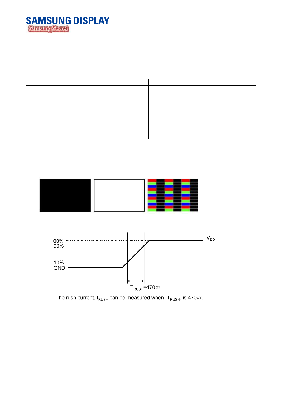
Main frequency Fdclk 72 78 85 MHz
Rush current IRUSH
Note (1) The ripple voltage should be controlled fewer than 10% of V
(2) fV=60Hz, fDCLK = 78MHz, VDD = 12.0V, DC Current.
(3) Power dissipation check pattern (LCD Module only)
a) Black pattern b) White pattern c) V-stripe
(a) Black
(b) White -
(d)V-Stripe -
IDD
- 400 500 mA
400 500
700 800
- -
2 A (4)
(Typ.) voltage.
DD
mA
mA
(2),(3)
(4) Conditions for measurement
——————————————————————————————————————————————––—
Doc.No. LSC320AN02 Page 9 of 36 Rev.No. 06-000-G-20121228
Symbol Description
Symbol Description
DC power supply
LVDS Signal +
DC power supply
DC power supply
LVDS Signal
DC power supply
LVDS Signal +
LVDS Option
LVDS Signal
LVDS Signal
LVDS Signal +
LVDS Signal
————————————————————————————————————————————————–
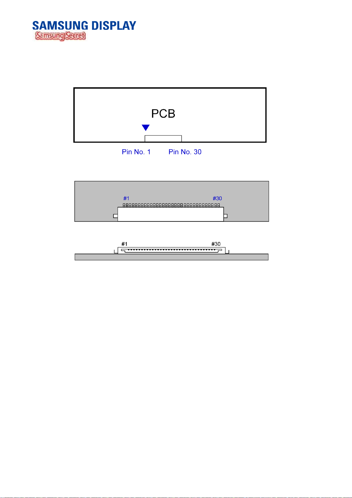
5. INPUT TERMINAL PIN ASSIGNMENT
5.1 INPUT SIGNAL & POWER
Connector : 187053-30091(P-TWO)
1
2
3
4
5
6
7
8
Pin
12V
12V
12V
12V
GND Ground
GND Ground
GND Ground
GND Ground
Pin
16
17
18
19
20
21
22
23
R1B_P
GND Ground
R1C_N
R1C_P
GND Ground
R1CLK_N LVDS Clock -
R1CLK_P LVDS Clock +
GND Ground
-
9
10
11
12
13
14
15
Note (1) No connection: These PINS are used only for the product of SAMSUNG.
(DO NOT CONNECT the input device to these pins.)
Note2) LVDS OPTION : If this PIN is HIGH (3.3 V) → Normal LVDS format
LOW (GND) → JEIDA LVDS format
LVDS SEL
NC NOTE1
GND Ground
R1A_N
R1A]P
GND Ground
R1B_N
-
-
24
25
26
27
28
29
30
R1D_N
R1D_P LVDS Signal +
GND Ground
B_INT I2C
SCL I2C
SDA I2C
GND Ground
-
——————————————————————————————————————————————––—
Doc.No. LSC320AN02 Page 10 of 36 Rev.No. 06-000-G-20121228
————————————————————————————————————————————————–
Note (2) Pin number which starts from the left side.
a. Power GND pins should be connected to the LCD’s metal chassis.
b. All power input pins should be connected together.
c. All NC pins should be separated from other signal or power.
Fig . The diagram of connector
——————————————————————————————————————————————––—
Doc.No. LSC320AN02 Page 11 of 36 Rev.No. 06-000-G-20121228
 Loading...