

Samsung LE26R71B Schematic
TFT-LCD TV
Chassis Model
GBD26KE LE26R71B
GBR26KE LE26R72B
GBD32KE LE32R71B
GBR32KE LE32R72B
GBR37KE LE37R72B
GBD40KE LE40R71B
GBR40KE LE40R72B
Manual
SERVICE
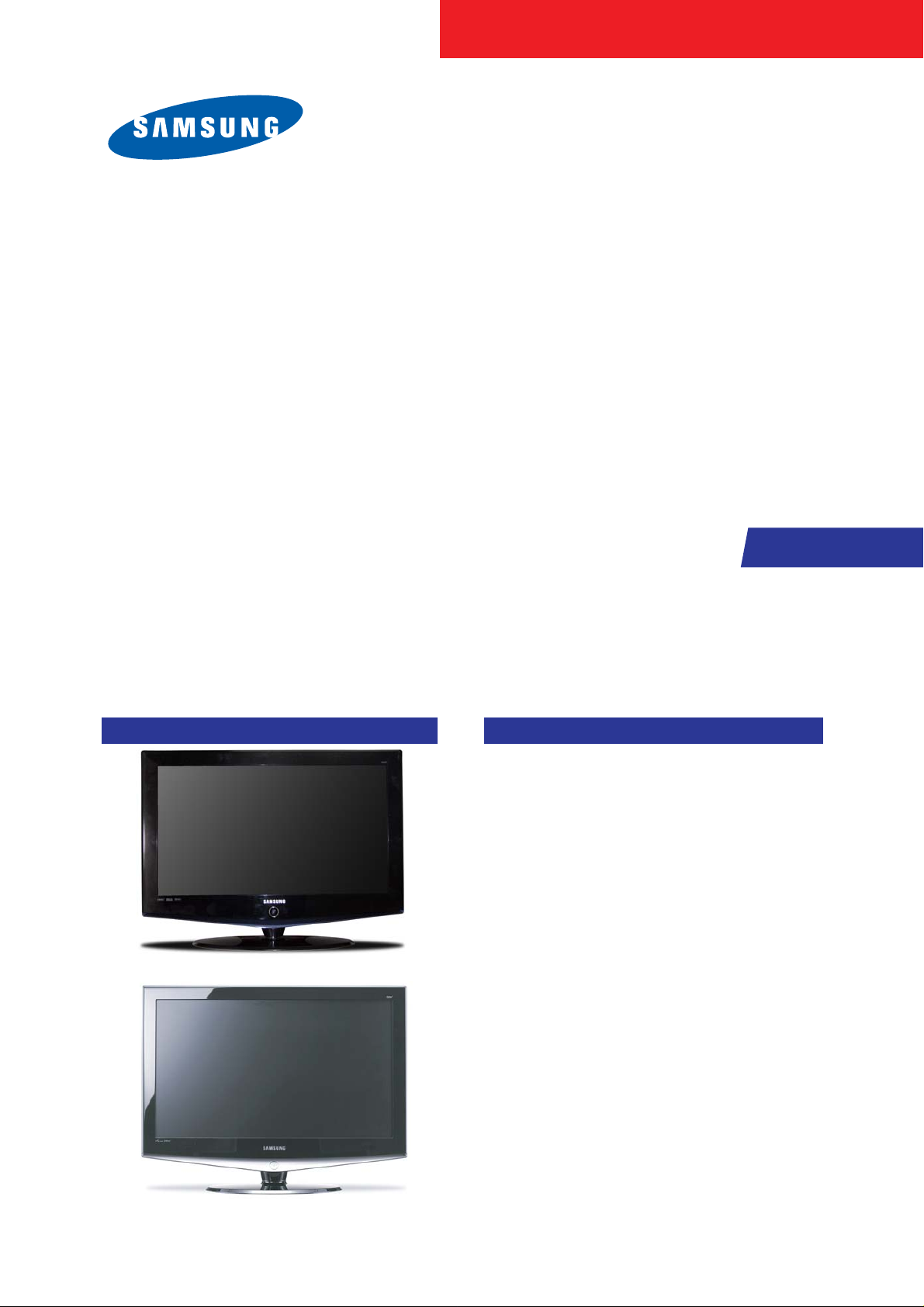
TFT-LCD TV Fashion Feature
- Luxurious Slim Design
- Supreme Picture Quality
- Supreme Sound Quality
- Supreme Convenience Quality
- Convenience for Users
LE26R71B,LE32R71B,LE40R71B
LE26R72B,LE32R72B,LE37R72B,LE40R72B
Samsung Electronics Co.,Ltd.
416, Maetan-3Dong, Yeongtong-Gu, Suwon City,
Gyeonggi-Do, Korea, 443-742
Printed in Korea
P/N : BN82-00139B-00
URL : http://itself.sec.samsung.co.kr/
- This Service Manual is a property of
Samsung Electronics Co., Ltd.
Any unauthorized use of Manual can be
punished under applicable International
and/or domestic law.

3 Alignments and Adjustments
3-1
3 Alignments and Adjustments
3-1 Ser vice Instr uction
1. Usually, a color TV-VCR needs only slight touch-up adjustment upon installation.
Check the basic characteristics such as height, horizontal and vertical sync.
2. Use the specified test equipment or its equivalent.
3. Correct impedance matching is essential.
4. Avoid overload. Excessive signal from a sweep generator might overload the front-end
of the TV. When inserting signal markers, do not allow the marker generator to distort
test result.
5. Connect the TV only to an AC power source with voltage and frequency as specified on
the backcover nameplate.
6. Do not attempt to connect or disconnect any wire while the TV is turned on. Make sure
that the power cord is disconnected before replacing any parts.
7. To protect aganist shock hazard, use an isolation transform.
3 Alignments and Adjustments
3-2
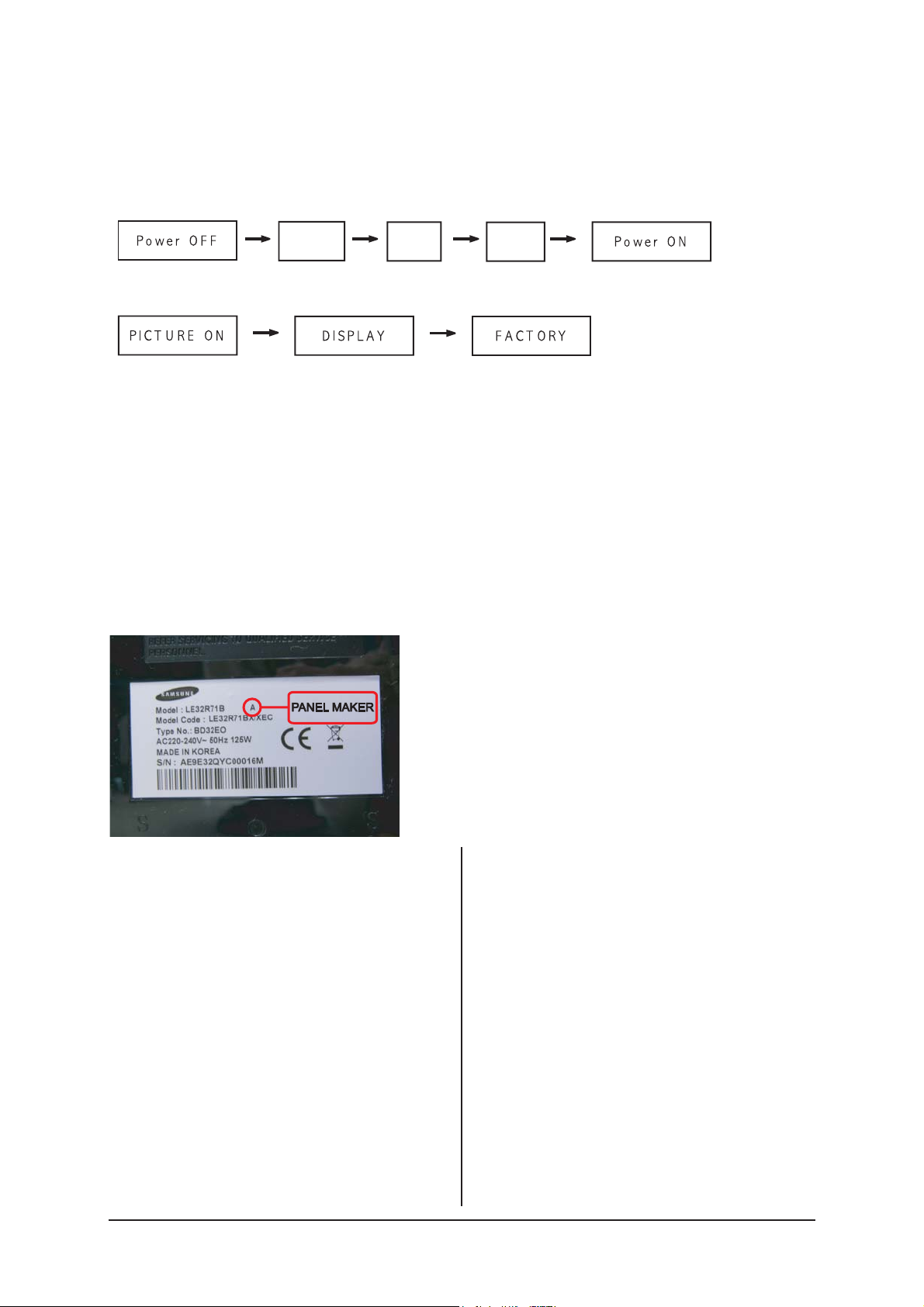
3-2 How to Access Service Mode
3-2-1 Entering Factory Mode
1. To enter "Service Mode" Press the remote -control keys in this sequence :
- If you do not have Factory remote - control
- If you have Factory remote - control
- The buttons are active in the service mode.
1. Remote - Control Key : Power, Arrow Up, Arrow Down, Arrow Left
Arrow Right, Menu, Enter, Number Key(0~9)
2. Function - Control Key : Power, CH +, CH -, VOL +, VOL -,
Menu, TV/VIDEO(Enter)
3-2-2 Panel Check
Specially for LE26,32R7**, You have to check Panel Maker Because of different adjustments as follows.
First of all, Check the label rating!
1) Label Rating File
If Panel Mark is "A", Set the factory mode
indicating as follows.
Panel BOM(Bill of material) : BN07-00289A
Connector between Panel and Power Unit
: BN39-00603M (300mm)
* Option Byte
1. Gamma "AUO"
2. Panel Option "AUO"
If Panel Mark is "S" or not printed.
Set the factory mode indicating as follows.
Panel BOM(Bill of material) : BN07-00247A
Connector between Panel and Power Unit
: BN39-00603M (300mm)
* Option Byte
1. Gamma "AMLCD"
2. Panel Option "AMLCD_INT"
If Panel Mark is "C" , Set the Factory mode
indicating as follows.
Panel BOM(Bill of Material) : BN07-00207A
Connecotor between Panel and Powe Unit :
BN39-00659A(200mm)
* Option Byte
1. Gamma " CMO "
2. Panel Option " CMO "
Others are same shown below.
INFO
MENU MUTE
3 Alignments and Adjustments
3-3
3-3 Factory Data
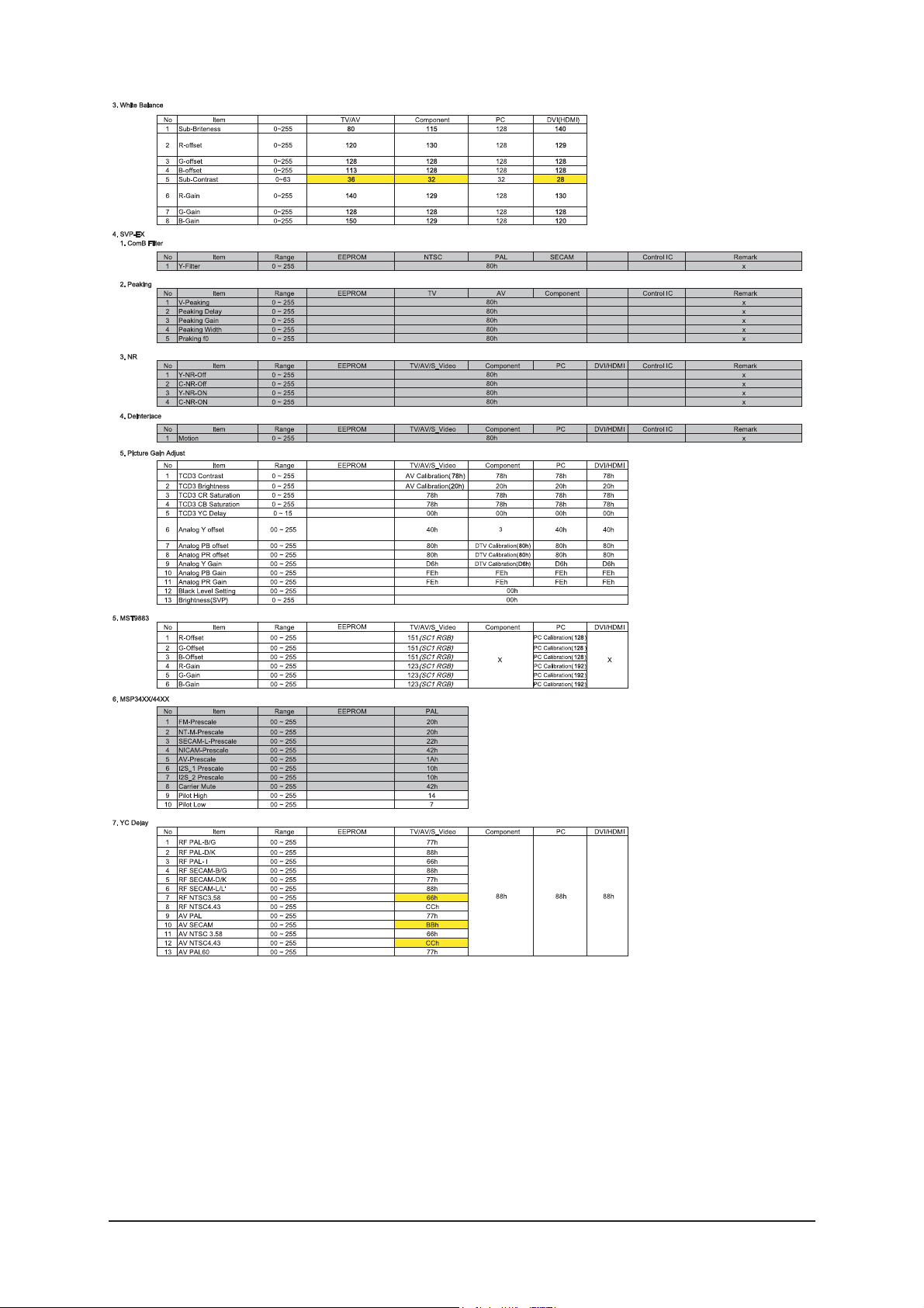
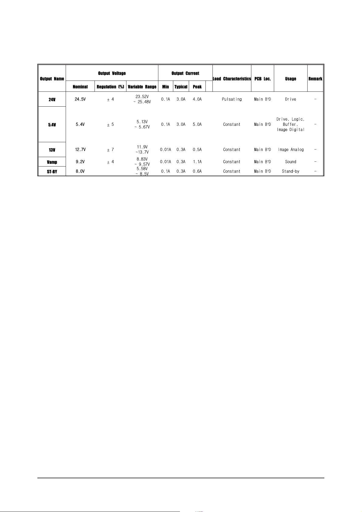
1. Calibration
2. Option Table XXXX XXXX
3. White Balance
4. SVP-FX
5. Option Block
6. STV8257/STA323W
7. YC Delay
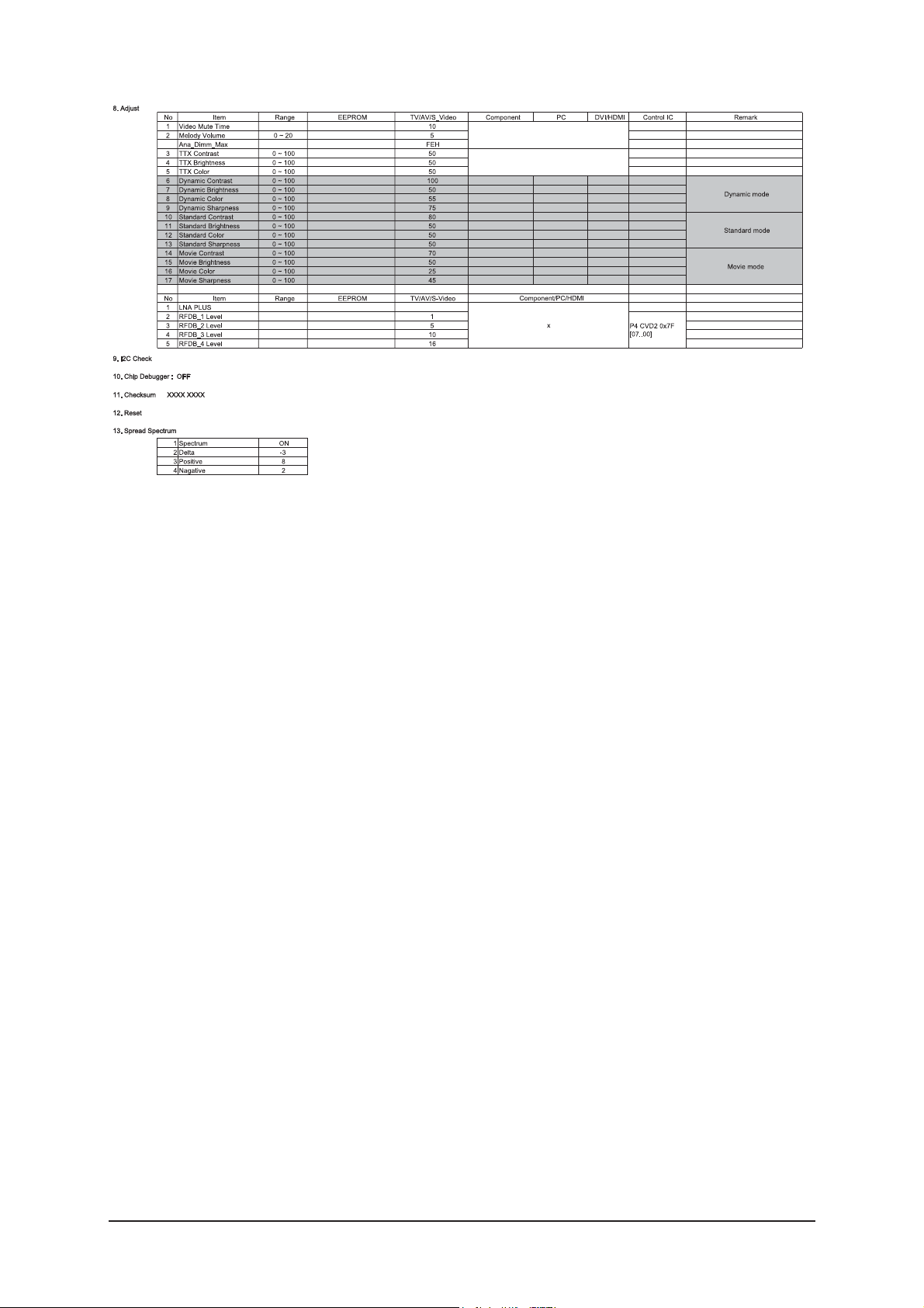
8. Adjust
9. I2C Check
10. W/B MOVIE
11. Checksum
12. Reset
13. Spread Spectrum
T-MILMPEU-1006 (Main Micom Ver)
T-MILMPEUS-1002 (Sub Micom Ver)
Month / Day / Year / Hour / Min. / Sec.
1. Calibration
1) AV Calibration
2) DTV Calibration
3) PC Calibration
2. Option Table XXXX XXXX
Inch Option 32" Carrier Mute ON TTX Group Auto
Gamma OFF Language English Auto Power ON
Panel Option AMLCD_INT Auto FM ON ---- OFF
2HDMI OFF High Deviation OFF ---- G
Brt.Sensor OFF TTX ON ---- OFF
EnergySave ON TTX List ON Debug OFF
LBE/FBE OFF ACR OFF Ch.Table SUWON
FRC(Micronas) OFF Dynamic CE ON iDTV_Cntry UK
FRC(Samsung) OFF Dynamic Dimming ON Dynamic Contrast OFF
LNA OFF Tuner TOP 10
3 Alignments and Adjustments
3-4
3 Alignments and Adjustments
3-5
3 Alignments and Adjustments
3-6
3-4 Ser vice Adjustment
3-4-1 White Balance - Calibration
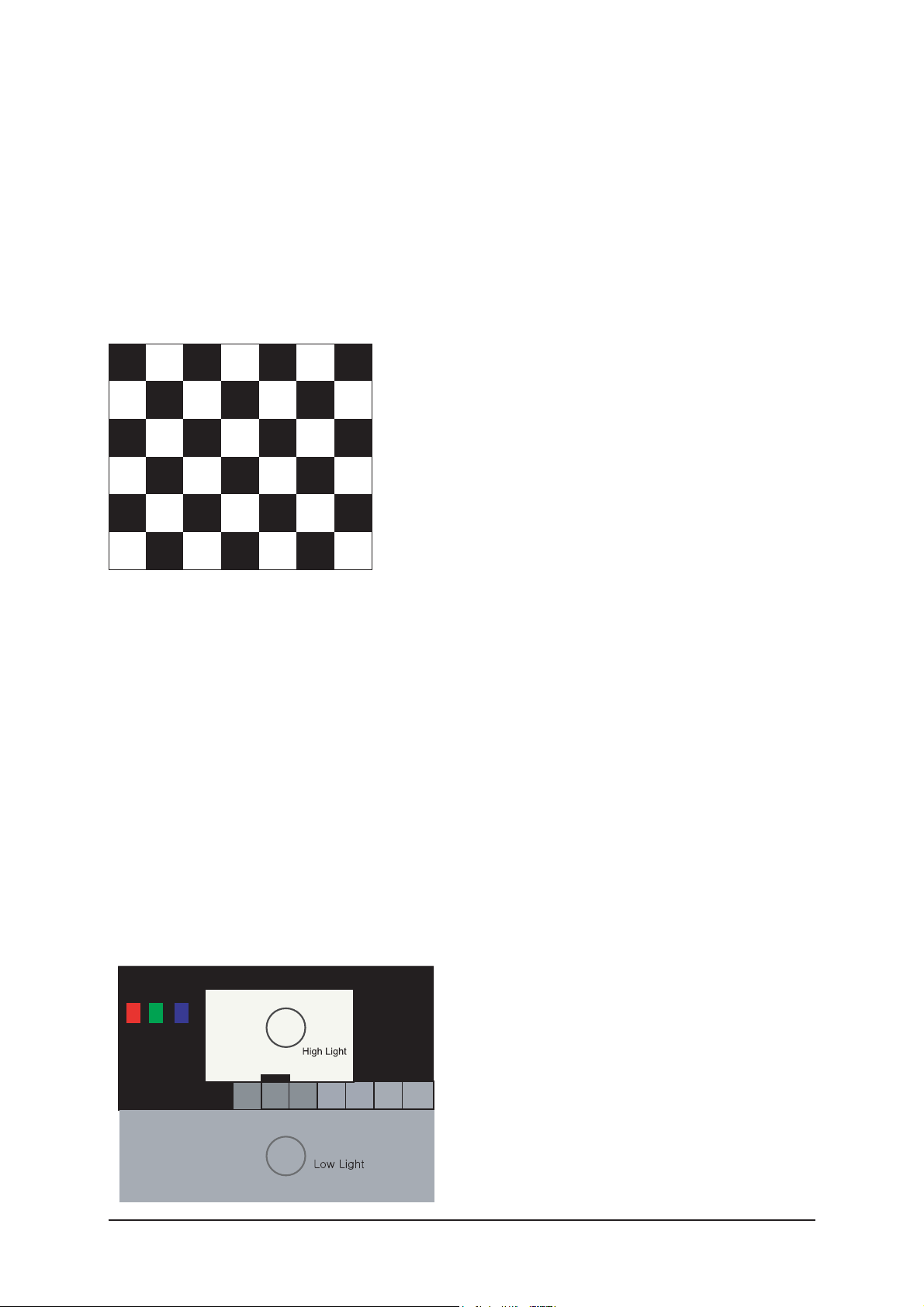
If picture color is wrong, do calibration first.
Equipment : CA210, Patten : chess pattern
Execute calibration in Factory Mode
Source AV : PAL composite, Component : 1280*720/60Hz
PC : 1024*768/60Hz
3-4-2 White Balance - Adjustment
If picture color is wrong, check White Balance condition.
Equipment : CA210, Patten : Toshiba
Adjust W/B in Factory Mode
Sub brightness and R/G/B Offset controls low light region
Sub contrast and R/G/B Gain controls high light region
Source AV : PAL composite, Component : 1280*720/60Hz
HDMI[DVI] : 1280*720/60Hz
Toshiba Patten
[ Test Pattern : MSPG-945 Series Pattern #16 ]
*Color temperature
1500K +/-500, -6 ~-20 MPCD
*Color coordinate
H/L : 267/263 +/- 2 35.0 Ft +/- 2.0Ft
L/L : 270/260 +/- 3 1.5 Ft +/- 0.2Ft
( chess patten )
3 Alignments and Adjustments
3-7
3-4-3 Conditions for Measurement
1. On the basis of toshiba ABL pattern : High Light level (57 IRE)
- INPUT SIGNAL GENERATOR : MSPG-925LTH
* Mode NO 2 : 744X484@60 Hz
NO 6 : 1280X720@60 Hz
NO 21 : 1024X768@60 Hz
* Pattern NO 36 : 16 Color Pattern
NO 16 : Toshiba ABL Pattern
2. Optical measuring device : CA210 (FL)
Please use the MSPG-925 LTH generator for model
LE26M51B/LE32M51B/LE40M51B/LE46M51B
.
3-4-4 Method of Adjustment
1. Adjust the white balance of AV, Component and DVI Modes.
(AV Component)
a) Set the input to the mode in which the adjustment will be made
(RF DTV PC DVI).
* Input signal - VIDEO Mode : Model #2 (744*484 Mode), Pattern #16
- DTV,DVI Mode : Model #6 (1280*720 Mode), Pattern #16
- HDMI Mode: Model #6(1280*720 Mode), Pattern #16
b) Enter factory color control, confirm the data.
c) Adjust the low light. (Refer to table 1, 2 in adjustment position by mode)
- Adjust sub - Brightness to set the 'Y' value.
- Adjust red offset ('x') and blue offset ('y') to the color coordinates.
* Do not adjust green offset data.
d) Adjust the high light. (Refer to table 1, 2 in adjustment position by mode)
- Adjust red gain ('x') and blue gain ('y') to the color coordinates.
* Do not adjust the green gain and sub-contrast (Y) data.
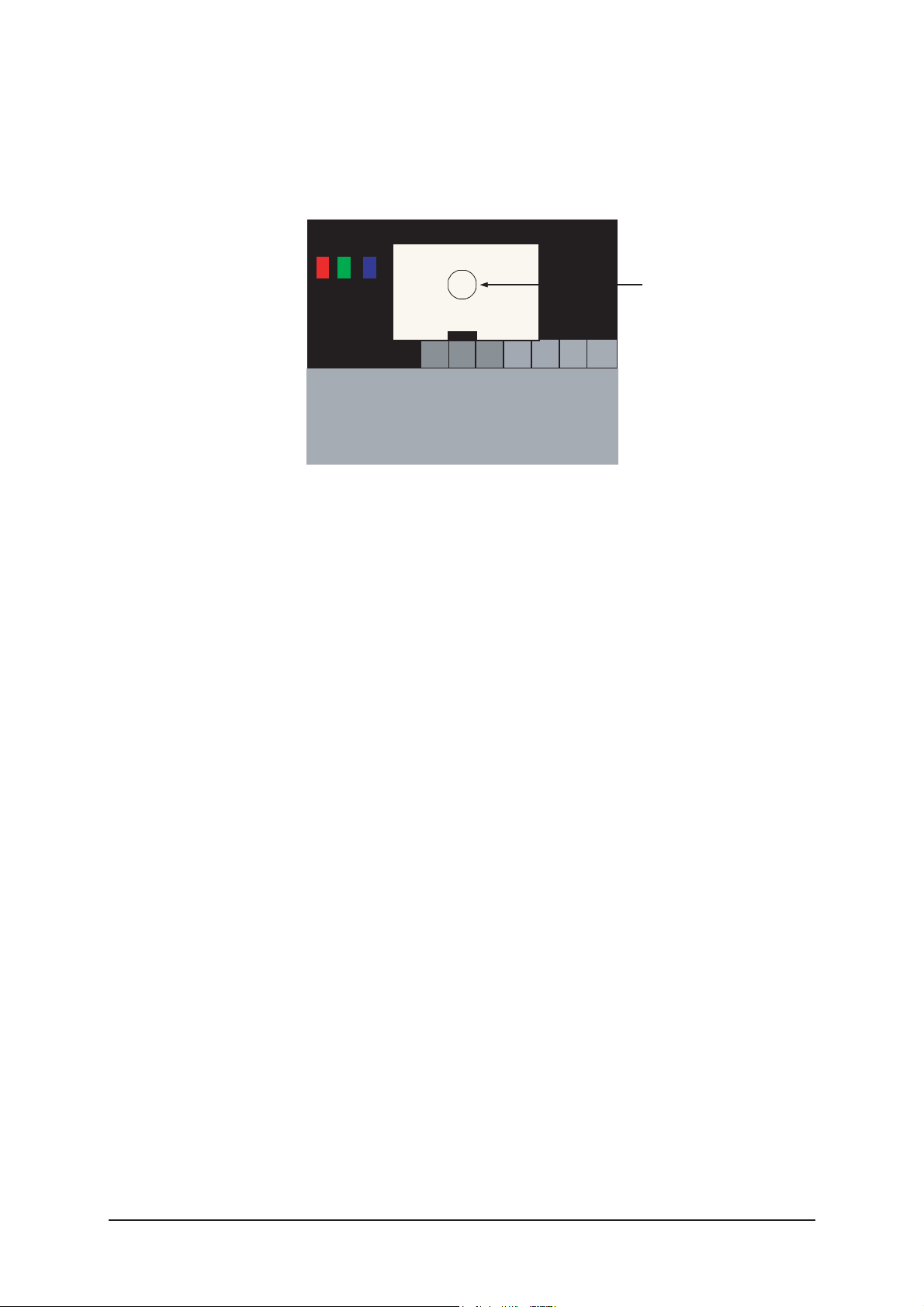
Picture 4-2 Toshiba ABL Pattern
Low light
Measurement point
3 Alignments and Adjustments
3-8
d) Adjust the high light. (Refer to table 1, 2 in adjustment position by mode)
- Adjust red gain ('x') and blue gain ('y') to the color coordinates.
* Do not adjust the green gain and sub-contrast (Y) data.
Picture 4-3 Toshiba ABL Pattern
High light
Measurement point
3 Alignments and Adjustments
3-9
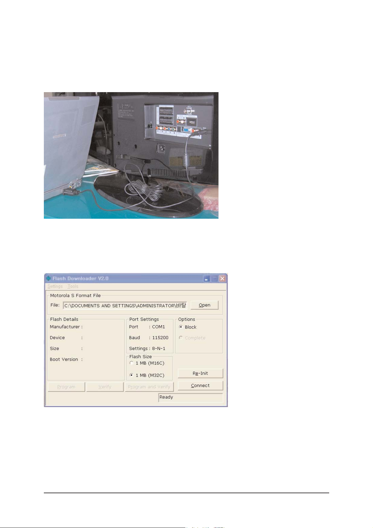
3-5 Software Upgrade
3-5-1 How to Update Flash ROM
1. Installthe Flash Downloader
ConnectSet(Service Jack)and Jig Cable to execute Program Update.
2. Flash Downloader program update
-Before Turning on the set,Click "connect"which is under of OSD Screen!
-Turn on the Set.

Memo
3 Alignments and Adjustments
3-10
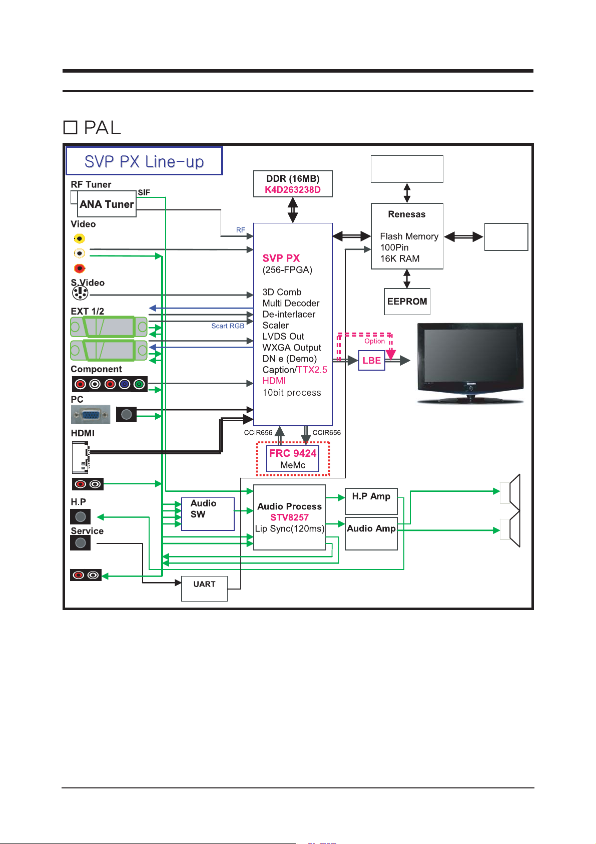
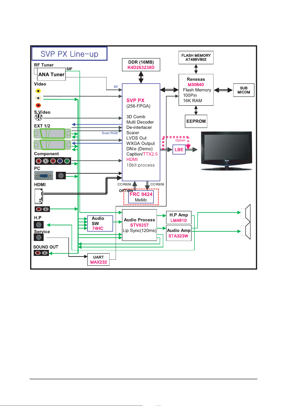
7 Block Diagrams
7-1
7 Block Diagram
- This Document can not be used without Samsung’s authorization
M30840
LM4810
74HC
OPTION
STA323W
MAX232
SOUND OUT
FLASH MEMORY
AT49BV802
SUB
MICOM

7 Block Diagrams
7-2
Memo
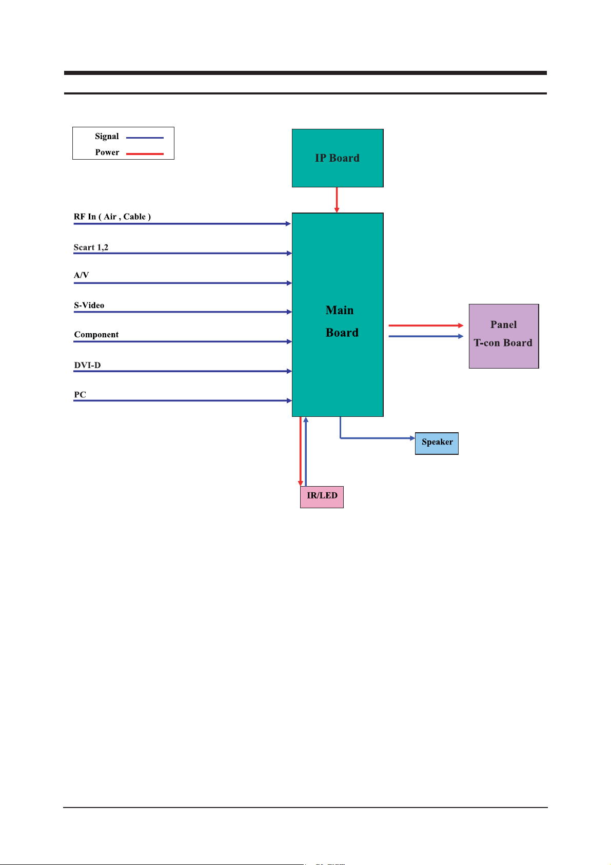
13 Circuit Descriptions
13-1
13 Circuit Descriptions
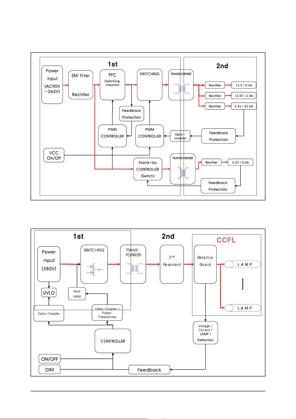
13-1 Block description
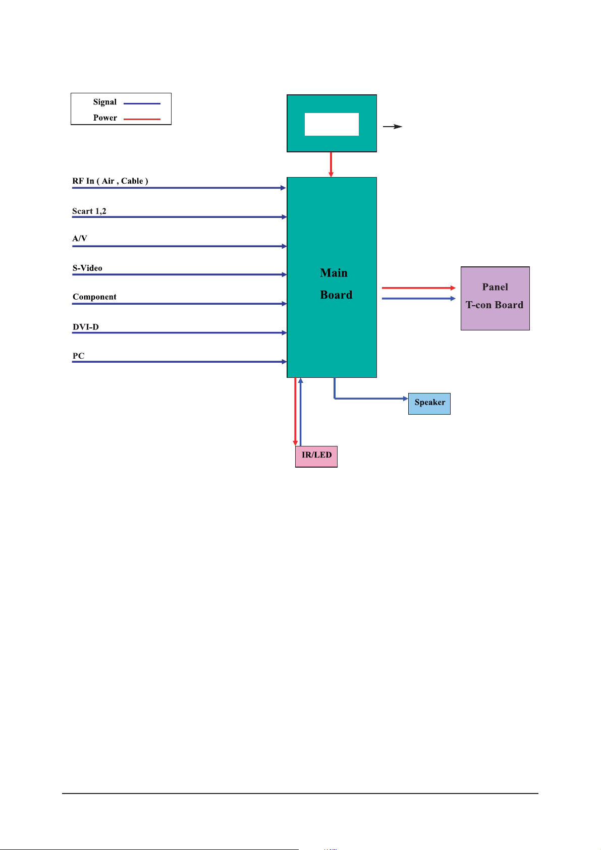
Bordeaux consists of three main blocks
1. Main board : Video signal processing
2. IP board : Power supply & Inverter
3. T-con board : LCD Panel control
13 Circuit Descriptions
13-2
Bordeaux consists of three main blocks
1. Main board : Video signal processing
2. SMPS : Power supply
3. T-con board : LCD Panel control
SMPS
IINVERTER
13 Circuit Descriptions
13-3
13-2 Main Block
13 Circuit Descriptions
13-4
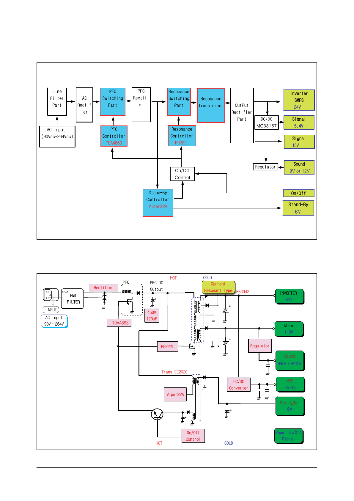
13-3 SMPS Board
13-3-1 26", 32" SMPS Block
13-3-2 26", 32" SMPS Block
13 Circuit Descriptions
13-5
13-3-3 26" , 32" SMPS Block
13-3-4 26" , 32" SMPS Block
13 Circuit Descriptions
13-6
13 Circuit Descriptions
13-7
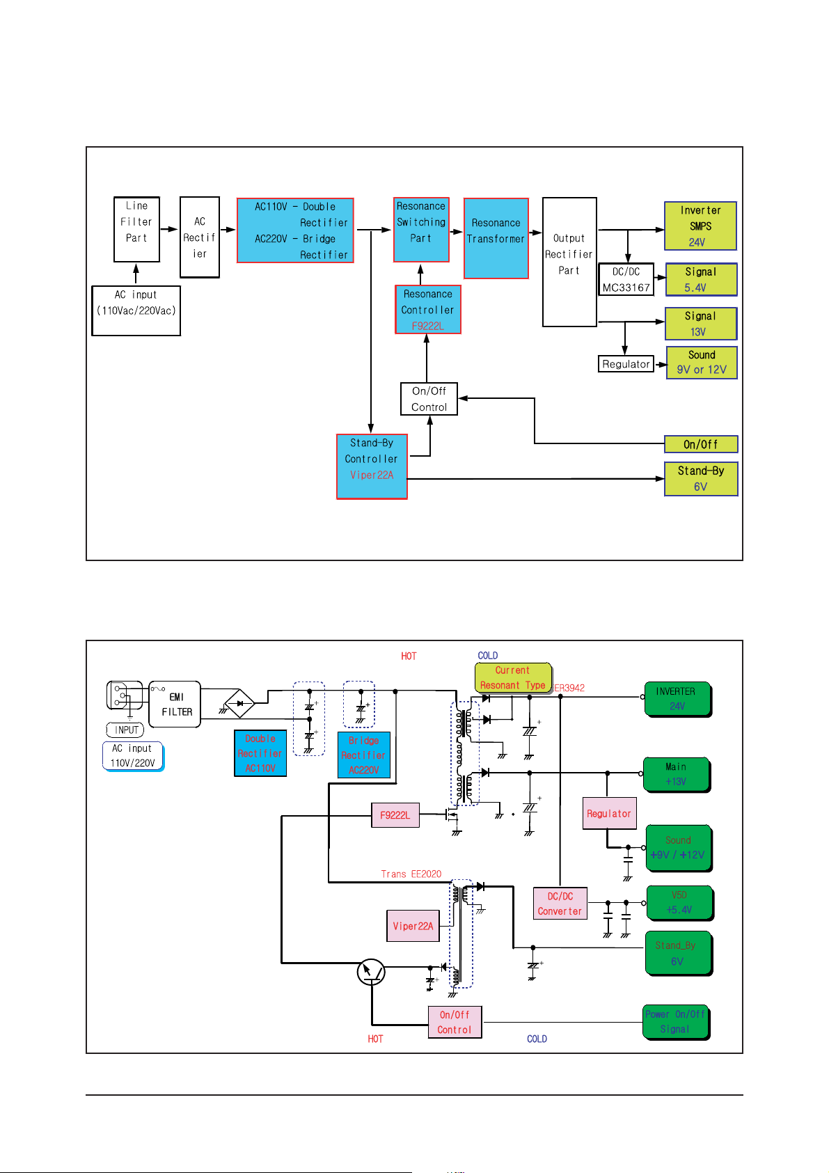
13-3-5 32" , 40" IP Board
13-3-6 32" , 40" IP Board

Memo
13 Circuit Descriptions
13-8

ii
Copyright
ⓒ 2006 by Samsung Electronics Co., Ltd.
All rights reserved.
This manual may not, in whole or in part, be copied,
photocopied, reproduced, translated, or converted to any
electronic or machine readable form without prior
written permission of Samsung Electronics Co., Ltd.
LE26R71B/LE26R72B/LE32R71B/LE32R72B/
LE37R72B/LE40R71B/LE40R72B Service Manual
First edition March 2006.
Printed in Korea.
Trademarks
Samsung is the registered trademark of Samsung
Electronics Co., Ltd.
LE26R71B/LE26R72B/LE32R71B/LE32R72B/
LE37R72B/LE40R71B/LE40R72B and Macmaster
Cable Adapter are trademarks of Samsung Electronics
Co., Ltd.
Macintosh and Power Macintosh are trademarks of
Apple Computer, Inc.
All other trademarks are the property of their respective
owners.

Contents
11. Precautions
………………………………………………………………………………………………………………………………………
11-1
1-1 Safety Precautions ……………………………………………………………………………………………………………………… 1-1
1-2 Servicing Precautions …………………………………………………………………………………………………………………… 1-2
1-3 Static Electricity Precautions …………………………………………………………………………………………………………… 1-2
1-4 Installation Precautions…………………………………………………………………………………………………………………… 1-3
2
2. Product specifications
…………………………………………………………………………………………………………………………
22-1
2-1 Fashion Feature…………………………………………………………………………………………………………………………… 2-1
2-2 LE26R71B / LE26R72B Specifications ………………………………………………………………………………………………… 2-2
2-3 LE32R71B / LE32R72B Specifications ………………………………………………………………………………………………… 2-3
2-4 LE37R72B Specifications………………………………………………………………………………………………………………… 2-4
2-5 LE40R71B / LE40R72B Specifications ………………………………………………………………………………………………… 2-5
2-6 Spec Comparison ………………………………………………………………………………………………………………………… 2-6
2-7 Option Specification ……………………………………………………………………………………………………………………… 2-7
3
3. Alignments and Adjustments
…………………………………………………………………………………………………………………
3
3-1
3-1 Service Instruction ……………………………………………………………………………………………………………………… 3-1
3-2 How to Access Service Mode …………………………………………………………………………………………………………… 3-2
3-3 Factory Data ……………………………………………………………………………………………………………………………… 3-3
3-4 Service Adjustment ……………………………………………………………………………………………………………………… 3-6
3-5 Software Upgrade ………………………………………………………………………………………………………………………… 3-9
4
4. Troubleshooting
………………………………………………………………………………………………………………………………
44-1
4-1 First Checklist for Troubleshooting ………………………………………………………………………………………………………4-1
4-2 Checkpoints by Error Mode ……………………………………………………………………………………………………………… 4-2
5
5. Exploded View and Parts List
…………………………………………………………………………………………………………………
55-1
5-1 LE26R71B Exploded View ……………………………………………………………………………………………………………… 5-1
5-2 LE26R71B Parts list ……………………………………………………………………………………………………………………… 5-2
5-3 LE26R72B Exploded View ……………………………………………………………………………………………………………… 5-3
5-4 LE26R72B Parts list ……………………………………………………………………………………………………………………… 5-4
5-5 LE32R71B Exploded View ……………………………………………………………………………………………………………… 5-5
5-6 LE32R71B Parts list ……………………………………………………………………………………………………………………… 5-6
5-7 LE32R72B Exploded View ……………………………………………………………………………………………………………… 5-7
5-8 LE32R72B Parts list ……………………………………………………………………………………………………………………… 5-8
5-9 LE37R72B Exploded View ……………………………………………………………………………………………………………… 5-9
5-10 LE37R72B Parts list …………………………………………………………………………………………………………………… 5-10
5-11 LE40R71B Exploded View …………………………………………………………………………………………………………… 5-11
5-12 LE40R71B Parts list …………………………………………………………………………………………………………………… 5-12
5-13 LE40R72B Exploded View …………………………………………………………………………………………………………… 5-13
5-14 LE40R72B Parts list …………………………………………………………………………………………………………………… 5-14
6
6. Electrical Parts List
……………………………………………………………………………………………………………………………
66-1
6-1 LE26R71BX/XEH Parts List……………………………………………………………………………………………………………… 6-1
6-2 LE26R72BX/XEC Parts List …………………………………………………………………………………………………………… 6-20
6-3 LE32R71BX/XEC Parts List …………………………………………………………………………………………………………… 6-34
6-4 LE32R72BX/XEH Parts List …………………………………………………………………………………………………………… 6-49

Contents
6-5 LE37R72BX/XEC Parts List …………………………………………………………………………………………………………… 6-63
6-6 LE40R71BX/BWT Parts List …………………………………………………………………………………………………………… 6-77
6-7 LE40R72BX/XEC Parts List …………………………………………………………………………………………………………… 6-92
7
7. Block Diagram
…………………………………………………………………………………………………………………………………
77-1
8. WWiring Diagram
…………………………………………………………………………………………………………………………………
88-1
8-1 LE26R71B/LE32R71B/LE40R71B/LE26R72B/LE32R72B/LE37R72B/LE40R72B Wiring Diagram …………………………… 8-1
8-2 Main Board Layout ……………………………………………………………………………………………………………………… 8-2
8-3 PIN characteristic ………………………………………………………………………………………………………………………… 8-3
8-4 Power Board Layout ……………………………………………………………………………………………………………………… 8-6
99. Schematic Diagrams
……………………………………………………………………………………………………………………………
99-1
9-1 Power_Sound Schematic Diagram ……………………………………………………………………………………………………… 9-1
9-2 Schematic Diagram ……………………………………………………………………………………………………………………… 9-2
9-3 Micom Schematic Diagram ……………………………………………………………………………………………………………… 9-3
9-4 SVP-PX/PX-Power/LBE-Option Schematic Diagram ………………………………………………………………………………… 9-4
9-5 Application Schematic Diagram ………………………………………………………………………………………………………… 9-5
1
10. Operating Instructions and Installation
………………………………………………………………………………………………………
110-1
10-1 Front …………………………………………………………………………………………………………………………………… 10-1
10-2 Connection Panel ……………………………………………………………………………………………………………………… 10-2
10-3 Remote control ………………………………………………………………………………………………………………………… 10-4
10-4 Installation the Stand ………………………………………………………………………………………………………………… 10-5
1
11. Disassembly and Reassembly
………………………………………………………………………………………………………………
111-1
11-1 Disassembly …………………………………………………………………………………………………………………………… 11-1
11-2 Reassembly …………………………………………………………………………………………………………………………… 11-5
1
12. PCB Diagram
…………………………………………………………………………………………………………………………………
112-1
12-1 26" Main PCB Diagram ……………………………………………………………………………………………………………… 12-1
12-2 32", 40" Main PCB Diagram ……………………………………………………………………………………………………………12-2
12-3 26" SMPS ……………………………………………………………………………………………………………………………… 12-3
12-4 32" SMPS ……………………………………………………………………………………………………………………………… 12-4
12-5 40" IP Board …………………………………………………………………………………………………………………………… 12-5
113. Circuit Descriptions
……………………………………………………………………………………………………………………………
113-1
13-1 Block description ……………………………………………………………………………………………………………………… 13-1
13-2 Main Block ……………………………………………………………………………………………………………………………… 13-3
13-3 SMPS Board …………………………………………………………………………………………………………………………… 13-3
1
14. Reference Infomation
………………………………………………………………………………………………………………………
114-1
14-1 Technical Terms ……………………………………………………………………………………………………………………… 14-1
14-2 Pin Assignments ……………………………………………………………………………………………………………………… 14-4
14-3 Timing Chart …………………………………………………………………………………………………………………………… 14-7
14-4 Panel Description …………………………………………………………………………………………………………………… 14-11
11 Disassembly and Reassembly
11-1
11 Disassembly and Reassembly
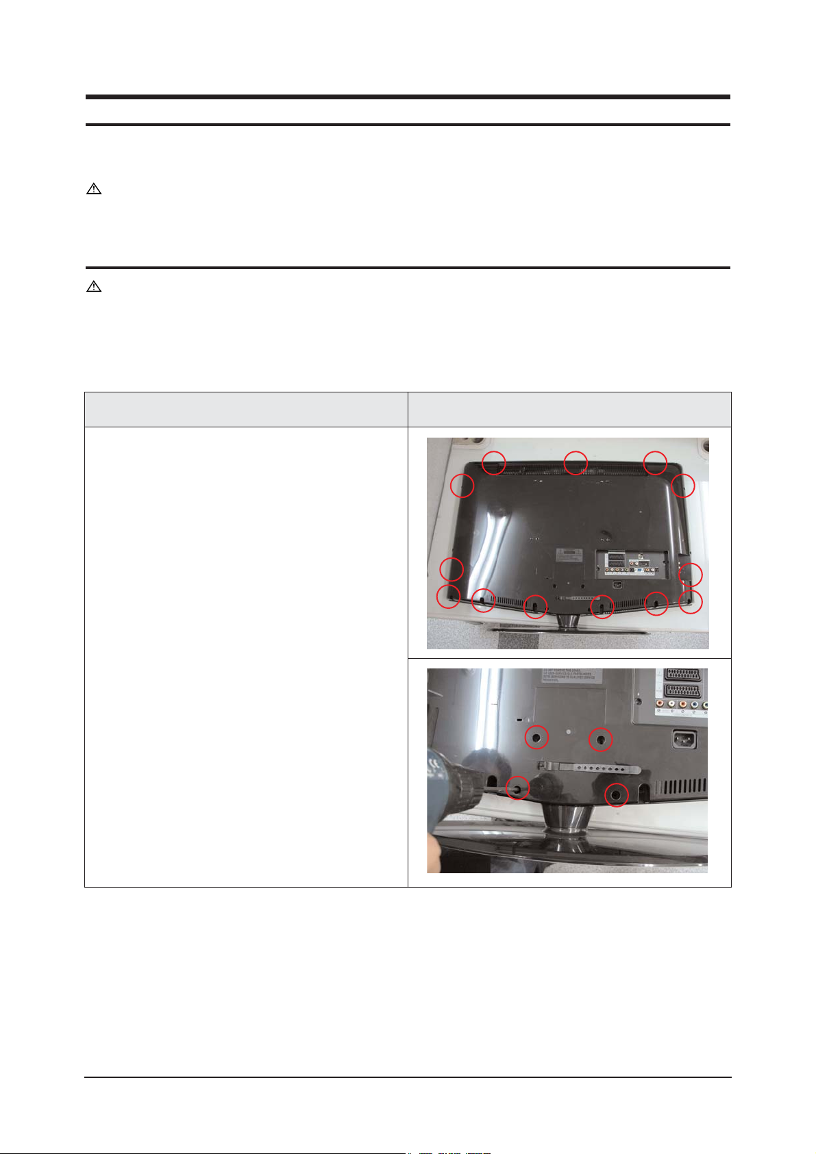
This section of the service manual describes the disassembly and reassembly procedures for the TFT-LCD
TV.
WARNING : This monitor contains electrostatically sensitive devices. Use caution when
handling these components.
11-1 Disassembly
Cautions : 1. Disconnect the monitor from the power source before disassembly.
2. Follow these directions carefully; never use metal instruments to pry apart the
cabinet.
Description Picture Description
1. Place monitor face down on cushioned table.
Remove screws from the rear cover.
Remove screws from the stand.
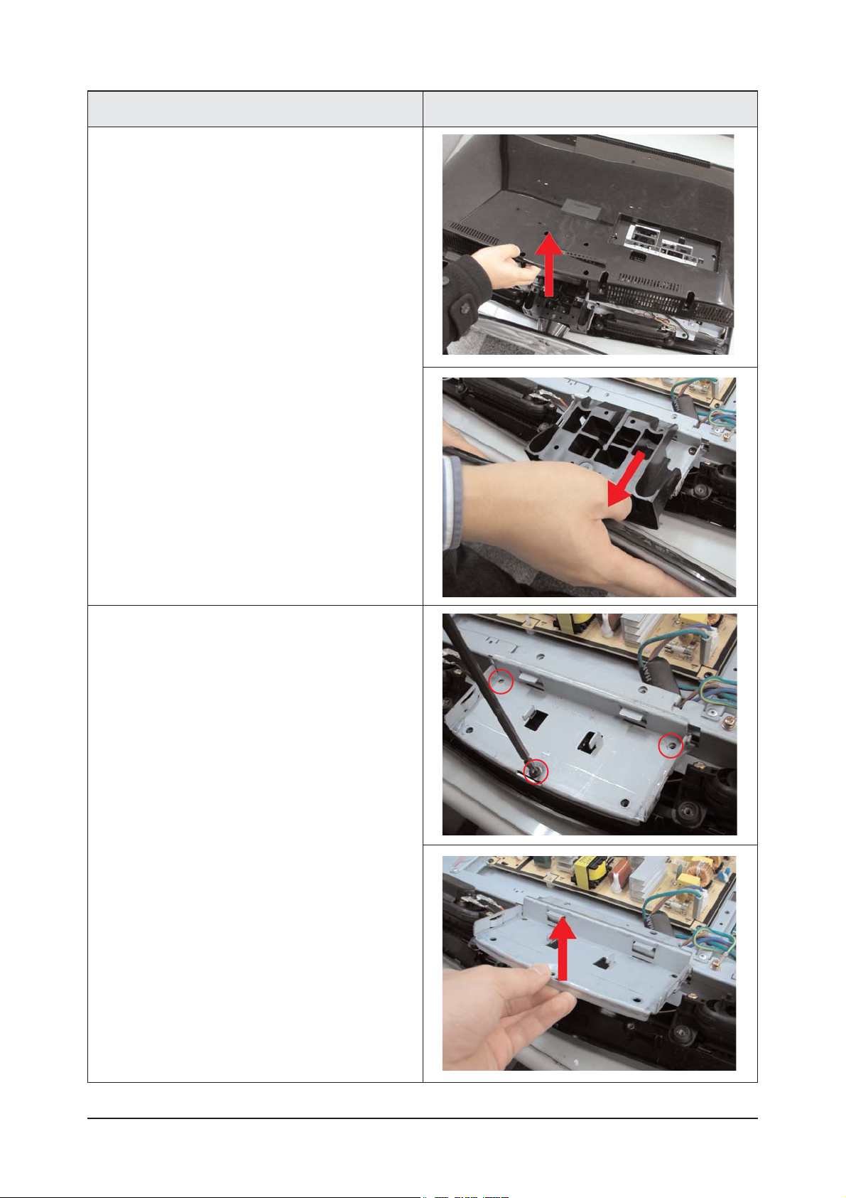
11 Disassembly and Reassembly
11-2
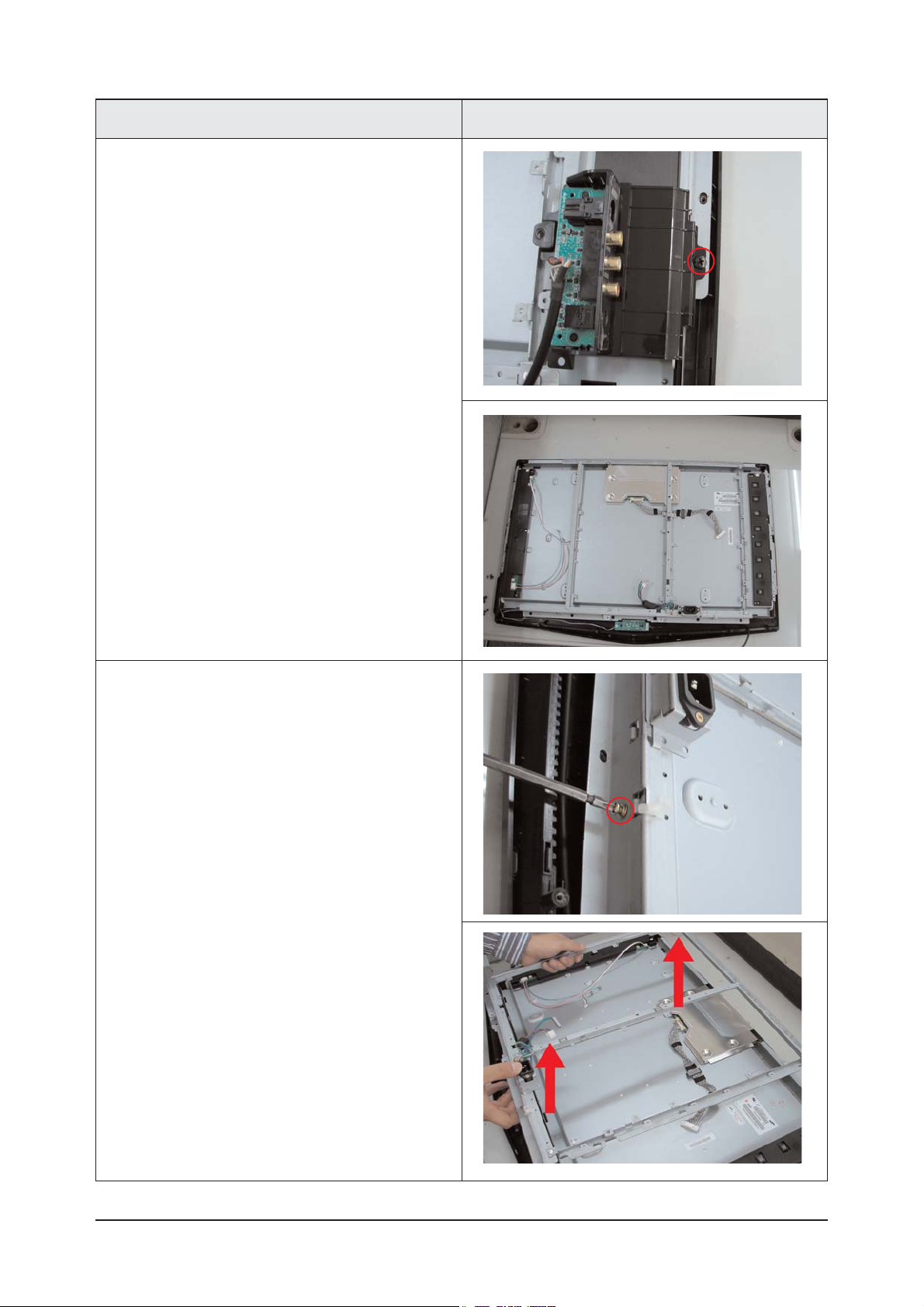
3. Remove Screws from the stand BRKT and lift
up the stand BRKT.
Description Picture Description
2. Lift up the rear cover and remove the stand.
11 Disassembly and Reassembly
11-3
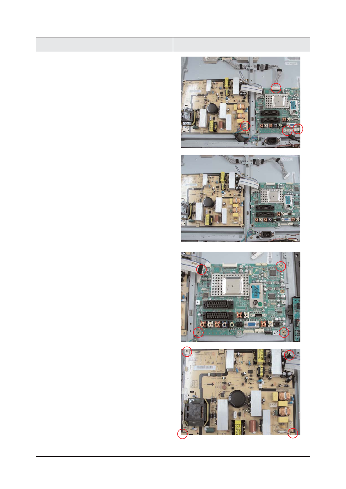
5. Remove screws from the boards and lift up the
boards.
Description Picture Description
4. Disonnect cable from the boards.
11 Disassembly and Reassembly
11-4
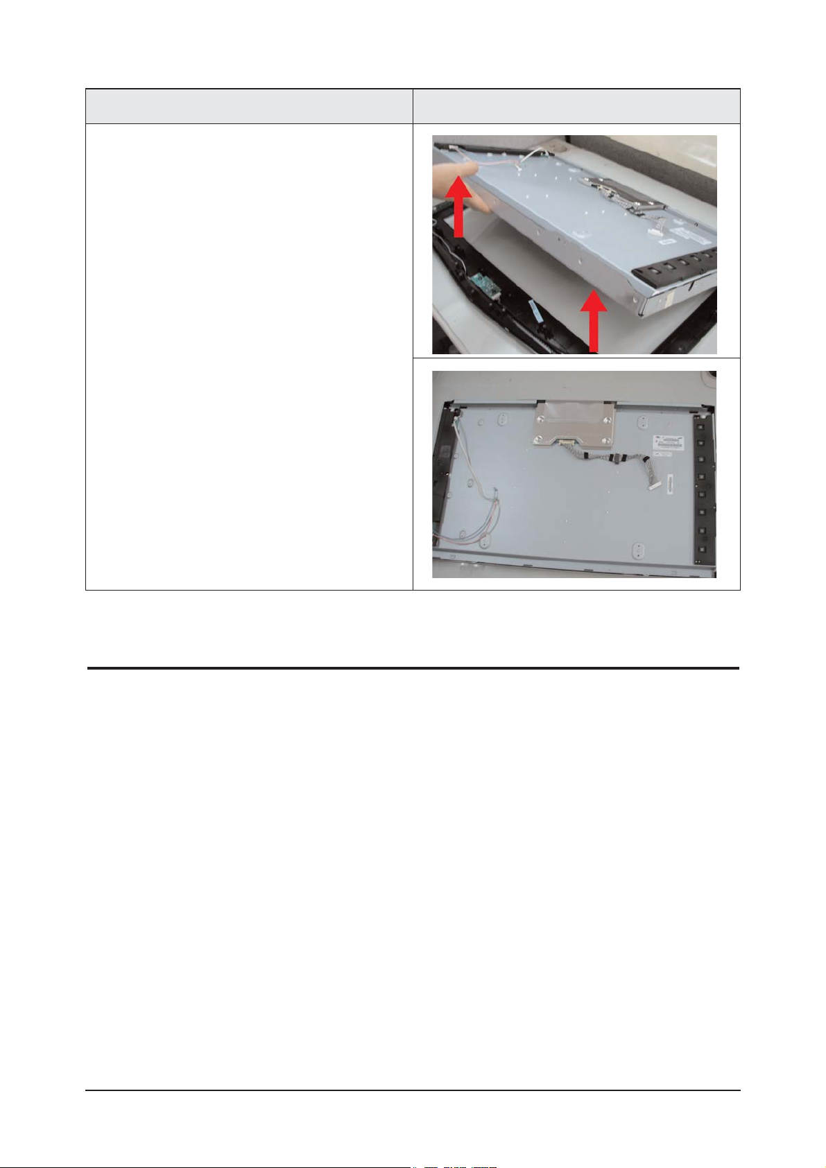
7. Lift up the panel BRKT.
Description Picture Description
6. Remove screw from the side connector.
Remove screws from the panel BRKT.
11 Disassembly and Reassembly
11-5
Description Picture Description
8. Lift up the LCD panel.
11-2 Reassembly
Reassembly procedures are in the reverse order of disassembly procedures.
 Loading...