

Samsung laptop 5 Schematic Diagram
X10
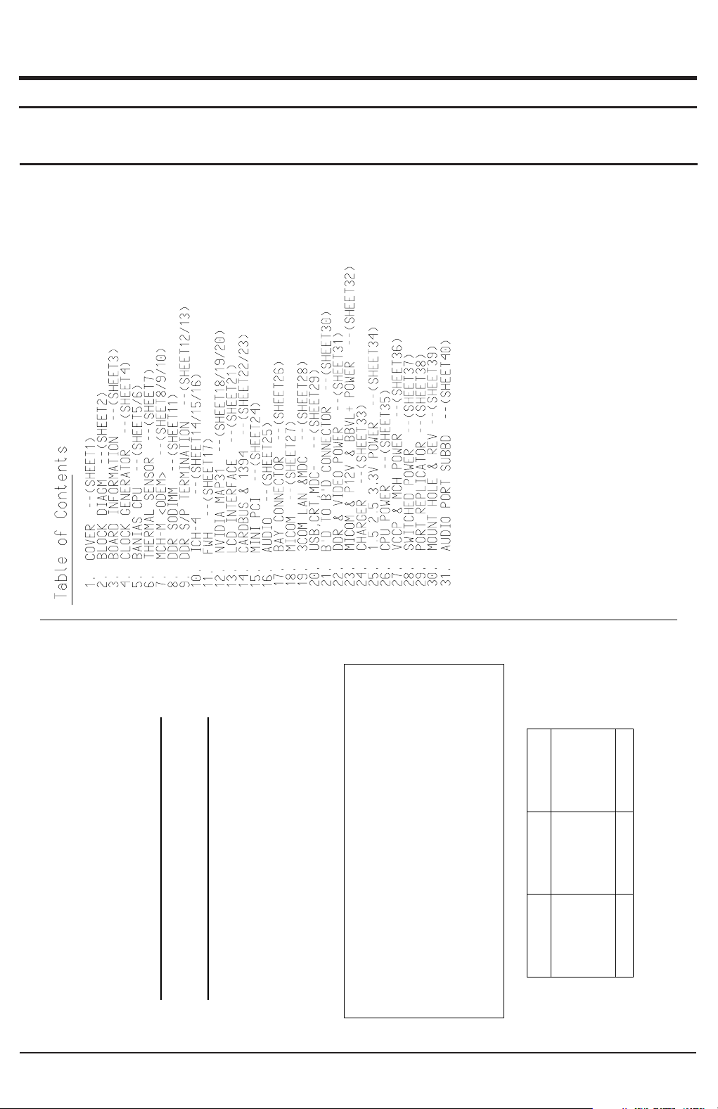
7-1 MAIN BOARD
7-1-1 Schematic Diagrams
7-1
7 Schematic Diagrams and PCB Silkscreen
TEMP
AQUILA
MCH-M ODEM
Dev. Step :
DRAW
PBA Name :
AQUILA MAIN
APPROVAL
Model Name :
P4-BANIAS
Revision :
BA92-01774A
CHECK
SR
Remarks :
PCB Code :
BA41-#####A
1.0
CPU :
Chip Set :
7 Schematic Diagrams and PCB Silkscreen
X107-2
LOW PIN COUNT
CIRRUS LOGIC S
GRAPHIC
593 FCBGA
ICH4 - M
TV (S-VHS)
EXTERNAL MIC
SYSTEM MEMORY
cs4202
MAX 512MBYTE EACH
LOM
FWH
BLUETOOTH
FINGER PRINT
TOUCHPAD
PS /2
SERIAL I/O
PARALLEL I/O
AC97 LINK
PC87393
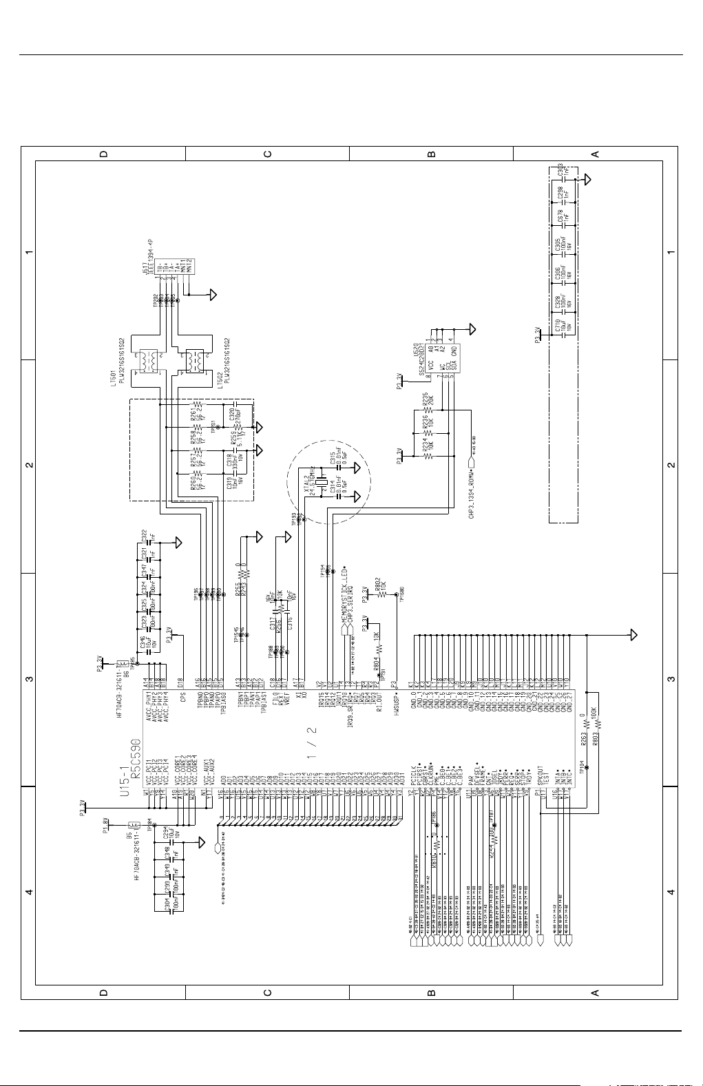
RICOH R5C590
PORT REPLICATOR
479 MICRO FCBGA
MICOM
2 EA SODIMM
WLAN &
HD64F2169
82801 DBM 1.5V
DOUBLE DATA RATE
USB 0 , 1
COMBO
USB 3
RJ -45
MCH-M
HDD
SLIM
3C920 - ST05
USB 2
BLUETOOTH
ODEM 1.2 V
CARDBUS
KEYBOARD
PCI BUS
MDC
1394 <PORT 0>
MINI PCI
IDE 0
200 / 266 MHZ
HEAD PHONE
nvidia MAP31
CPU <P4-BANIAS>
TFT_LCD 14.1"
AGP 4X , 1.5V
COMBO
INNER SPEAKER
IDE 1
2 USB
3 COM S
AUDIO CODEC
SPDIF
IDE 0
HITACHI S
PCI BUS
PSB 400MHZ
CARDBUS
EXTERNAL
IDE 1
AC97 LINK
WLAN
SUPER I/O
RJ -11
port replicator
MEMORY STICK
USB 4,5
421 FCBGA
CRT
HUB I / F
1.8V 8BIT 66MHZ
CONTROLLER
DVD-CD/RW
DC - IN
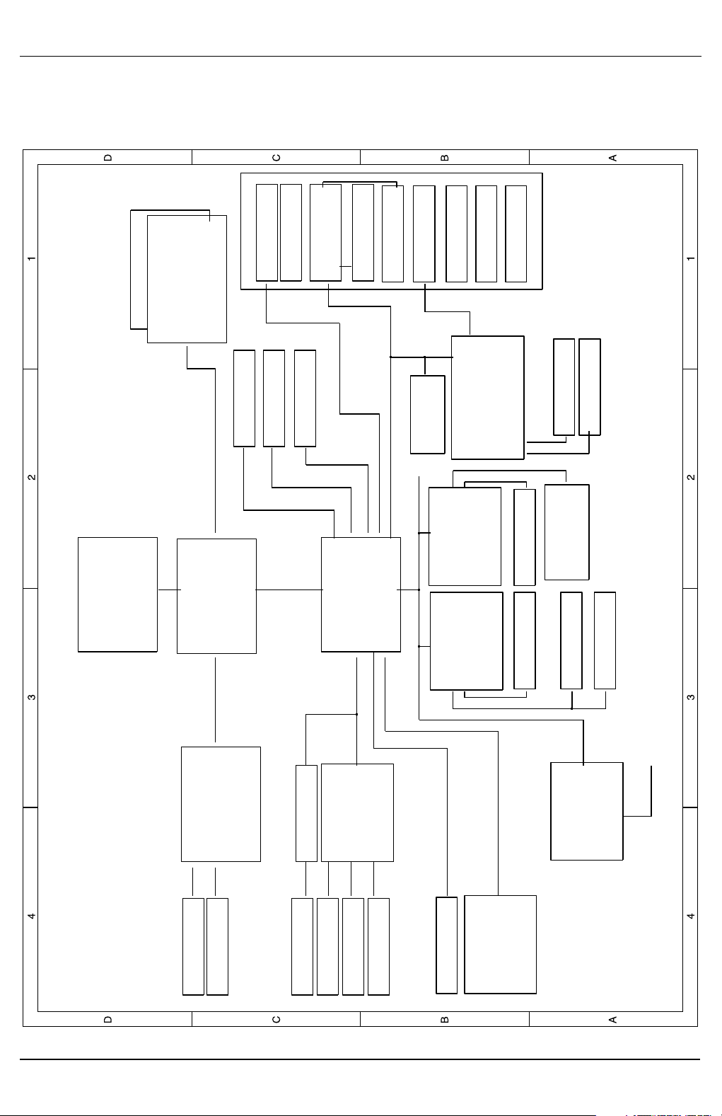
7-1-1(a) Main Board Schematic Sheet 2 of 39(Operation Block Diagram)
7 Schematic Diagrams and PCB Silkscreen
7-3X10
1
1
VID0
1
0
0
1
0
1
0
0.972 V
0
1.164 V
1
1
1
1
1.644 V
1.628 V
1.148 V
1.132 V
0.844 V
1
1.004 V
1.660 V
1
1
1
1
VID5
1.596 V
0
0
010
0
1
Devices
1
VID1
0
0
1
1
1
USB
0
00
-
0
1
0
Internal MAC
0
0
0
1
0
0
1
0
1
11
1
0
1
0
AD29(internal)
1.676 V
1.516 V
0
0
0
0
AD31(internal)
AD17(internal)
0
1
-
Note that this state does not preclude power being removed from non-essential devices, such as disk drives. During this state, CPU can be selected
0
0.860 V
USB2.0 #0 : A
B
VID3 VID2
9Ch
A0h
1
1
0
Devices
1
1
A2h
D2h
0
0
ICH4
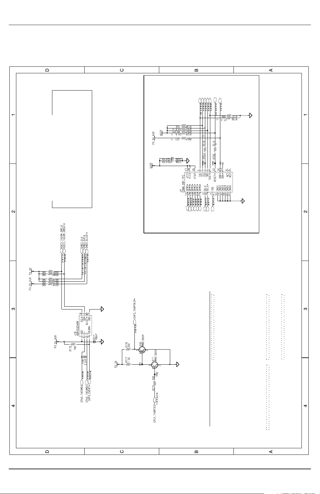
ADM1032(CPU Thermal Sensor)
0
0
1.5V switched power rail (off in S3-S5)
1.8V power rail(off in S4-S5)
1
1
1.8V switched power rail (off in S3-S5)
VDC
1
0
REVISION HISTORY
See rev notes in the changes file for more information.
1
0
AD19
1
0
1
2 E,F
0
1
Deeper Sleep
VCC_CORE
1
0
1001 110X
1010 0000
0
0.956 V
USB2.0 #1 : D
USB2.0 #2 : C
0
1
SMBUS Master
Thermal Sensor
0
1
-
I C / SMB Address
1.484 V
1.468 V
CK-408 (Clock Generator) 1101 001x
0
0
SCHEMATIC ANNOTATIONS AND BOARD INFORMATION
PCI Devices
0
0
VID4 Voltage
1
0
-
-
0
0
PORT NUMBER ASSIGNED TO
1.084 V
1
LPC bridge/IDE/AC97/SMBUS
AGP
Voltage Rails
Primary DC system power supply (7 to 21V)
3
PORT REPLICATOR
1.116 V
1
0
1
0
0
Memory is retained, and refreshes continue. All clocks stop except RTC clock.
CHP3_SLPS3* S3, Suspend-To-RAM(STR) : The system context is maintained in system DRAM, but power is shut off to non-critical circuits.
0.780 V
P1.5V
0
0
1
0
1
1
0.764 V
Lowest Freq.
0
1
0
1
Docking
PCI SLOT
1
1
1
1
1010 001X
Bus
3.3V always on power rail for MICOM
3.3V power rail (off in S4-S5)
AD21
P5V_ALWAYS
0
1
-B
P5V
P2.5V_AUX
1
Address
0
1
Hex
-
0
0
0
E
Cardbus
0.940 V
-
Clock, Unused Clock Output Disable
1
0
Northwood-B
(Interposer B d)
1.340 V
1.324 V
SYSTEM PORT A
2
1
1
LAN
CPU Core Voltage Table
1.372 V
1.356 V
P1.8V_AUX
P1.8V
0
0
0
11
0
In Deeper Sleep, CPU voltage reduced in this state to reduce the leakage power.
AD23
1.564 V
1.548 V
0
AD30(internal)
1
0
AC Link
Master
0
0
0
A,B,C
0
1
AD20
Core voltage for BANIAS CPU (1.356 - 0.844V)
1
1
3
-
1
1
-
2
0
0
0
1
1
0
MICOM_P3V
P2.5V
0
0
1
IDSEL#
0
1
VID3
USB PORT Assign
0
1
1
Hub to PCI
1
1
1
0
0
1
D
0
1
1
PORT REPLICATOR
CHP3_SLPS1* S1, Powered-On-Suspend(POS) : In this state, all clocks(except the 32.768KHz clock) are stopped.
1
1.708 V
1.276 V
1
0
0
1
0
0
1
0
10
1
1
MiniPCI SLOT1
1.532 V
VID4
0
0
0.908 V
0.748 V
1
1
0
1
1
0
0.716 V
0.700 V
3.3V switched power rail (off in S3-S5)P3.3V
1
0
1
00
0
0
0
1.180 V
1.100 V
0
1
1
0
0
0
0
0
1
1.404 V
1
1
0
11
1
1.308 V
1.388 V
1
1
0
0
1
1
1
1
1
1
1.692 V
1.580 V
-
1
0
0
0
1
1.500 V
00
0
1
1
1
0
Voltage
0
0
1
0
1
0
0
1
0
0
1.068 V
0.876 V
0
-
0
1
1
0
1
0
10
0
0
0
1.036 V
0
0
1
0
1
VID5
0
1
1
0
1
0
1
1
1
11
1
1
1
1
1
1
1
1.612 V
1
1
0
0.924 V
0.988 V
0
1
1
0.892 V
0.732 V
0
0
1
0
0
0
0
1.196 V
1.228 V
1
0
0
--
0
1
1
0
0
1
1
1.020 V
1
1
1
1
1
1
1
1
1
1
1
0
1
1
1
1
0
0
0
1.452 V
1
1
1
0
0
1
1
1.292 V
0
0
5.0V switched power rail (off in S3-S5)
2.5V power rail (off in S4-S5)
1
1
1
0
A,B,C,D
BLUETOOTH
P12V
1.25V power rail (off in S4-S5)
0
1
0
1
Highest Freq.
AD30(internal)
0
1.052 V
1
0
-
0
0
1
11
0
5.0V always on power
4
0
0
The system context is maintained in system DRAM. Power is maintained to PCI, the CPU, memory controller, memory, and all other criticial subsystems.
0
1
1
1.5V power rail (off in S4-S5)
CHP3_SLP4S* S4, Suspend-To-Disk(STD) : The Context of the system is maintained on the disk. All power is then shut off to the system except for the logic required to resume.
1.260 V
1
System Power States
3.3V always on Power Rail
1
1
1.212 V
1
1
P1.5V_AUX
BANIAS/ODEM Processor System Bus(PSB) Termination (1.05V)VCCP
0
0
0
AD24(internal)
1
1
1
0
1
2.5V switched power rail (off in S3-S5)
1
A,B
Interrupts
MCH-M Core Voltage (1.2V)
0
1.244 V
0.812 V
REQ/GNT#
1.420 V
0
1
0
0
0.796 V
VID0
P1.25V_AUX
0
0
VID1
0
VID2
0
1
0
-
0
1
1
1.436 V
1
SODIMM0
SODIMM1
0
SYSTEM PORT B
1
1
1
5
1
0
0
01
1
FINGER PRINT
0
1
-
for either Deep Sleep or Deeper Sleep.
P3.3V_ALWAYS
Externally appears same as S5, but may have different wake events.
CHP3_SLPS5* S5, Soft Off(SOFF) : System context is not maintained. All power is shut off except for the logic required to restart. A full boot is required when waking.
1
0.828 V
12.0V switched power rail (off in S3-S5)
P3.3V_AUX
0
VCC_MCH-
0
1
0
0
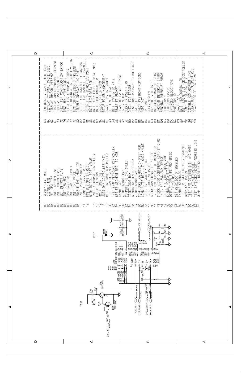
7-1-1(b) Main Board Schematic Sheet 3 of 39(Board Information)
7 Schematic Diagrams and PCB Silkscreen
X107-4
NO STUFF
0
200MHz
SEL0 HOST CLK
100MHz
NO STUFF
CY28346
1 1 133MHz
No Stuff
682088
1
option
1
ICS950810
P/N : 1209-001370
SEL1
No Stuff
0
0
OPTION
66MHz
0
CLK0_HCLK2
CLK0_HCLK2*
CLK0_ITP
CLK0_ITP*
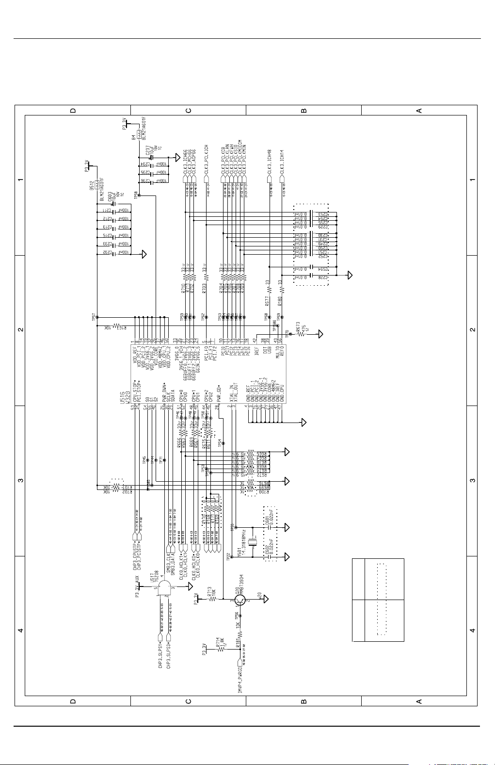
7-1-1(c) Main Board Schematic Sheet 4 of 39(Clock Generator)
7 Schematic Diagrams and PCB Silkscreen
7-5X10
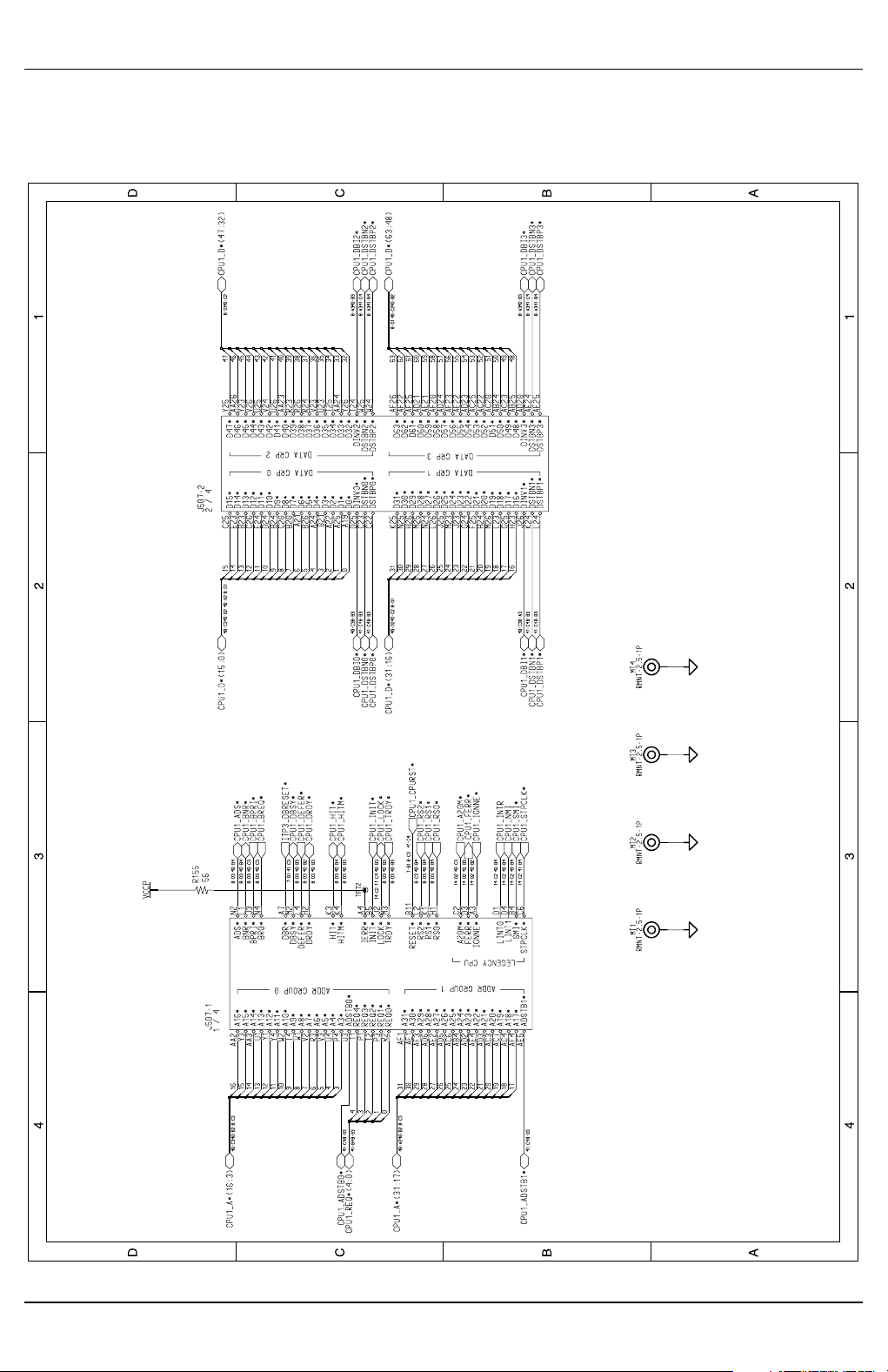
7-1-1(d) Main Board Schematic Sheet 5 of 39(Banias CPU)
7 Schematic Diagrams and PCB Silkscreen
X107-6
Placed as close as possible to
of the First GTLREF0 with Z0= 55 ohm trace
NO STUFF
Minimize coupling of any switching signals to this net
each of the four VCCA pins.
1/2 " to their respective Banias Pins
Z0=27.4 ohm (55 ohm) trace shorter than
VCCA, VCCQ CHECK ??
NO STUFF
STUFFING OPTION
NO STUFF
GTLREF : Keep the Voltage divider within 0.5"
COMP 0 , 2 <(COMP 1,3) should be connected
CLK0_HCLK2
CLK0_HCLK2*
CPU1_TDO
CPU1_BPM2*
CPU1_BPM0*
CPU1_BPM3*
CPU1_BPM1*
CPU1_PRDY*
CPU1_PREQ*
7-1-1(e) Main Board Schematic Sheet 6 of 39(Banias CPU)
7 Schematic Diagrams and PCB Silkscreen
7-7X10
0
0
0
0
1.164 V
1
1
0
0
1.052 V
VID0
1
1
1
0
0
0
0
OPTION
VID1
1.500 V
0
0
1
1
1.708 V
1
1
0
0
0
0
0
0
Voltage
0
0
1
1
1.484 V
0
1
1
0
1
0
0
1
11
0
01
1
1.212 V
Voltage
0
0
0
0
1.004 V
1
1
0
0
1
1
110
0
1
0
1
1
0
0
0
000
VID4
0
VID2
1
1
1
0
0
VID5
01
0
1.612 V
1100
0
VID0
1
1
1
0
1.468 V
1.532 V
0
1
0
1
0
0
1
1.180 V
VID3
0
1
1.196 V
1
1
1
1.148 V
1.084 V
101
0
1
0
1
1.116 V
0
0
0
0
0
0
1
1
001
0
0
1
0
0
1
1
-0
0
0
1
0
1
0
1.036 V
1
0
1.516 V
0
1
0 1.564 V
1.548 V
1
1
0
0
-0
1.436 V
1
1
0
1
000
1.244 V
0
- Keep traces away from fast data buses and CRT signal.
1.388 V
1.372 V
1 1.276 V
1.068 V
0
1
0.988 V
0
0
1.132 V
0
0
0
0
1
1
0
0
0
0
0
0
0.940 V
1
0
0
1
1
0
1.228 V
1
1
1.356 V 1
0
0
0
1
1
1
1
0
1.580 V
1
0
0
1
1
1.644 V
1
1.452 V
1
101
0
1
1.308 V
1.292 V
1
11
1
1
101
1
0
0.972 V
0.956 V
00
1 1.020 V
VID5
1
0
1
1
0
1
0
1
1
0.924 V
1.340 V
1.324 V
1
0
0.812 V
0.796 V
Northwood-B
0
0
0.700 V
0.876 V10.844 V
0
1
1
1
1
0
0
1
1
0
10
1
0
00
-
1
1
111
1
1
1
- Use guard traces flanking DXP and DXN and connecting to GND
1
1
111
0
1
00
1
1.100 V
1
1
1
1.692 V
0
0
0
1
1
1
0
0.908 V
0.748 V
0
0.828 V
Lowest Freq.
0
- Use recommended trace widths and spacings (10mil)
0
0
0.860 V00.764 V
0
1
0
0
1110
1
1
1.676 V
0
1
0
1
1
1
Refer To Thermal Sensor Layout Guidelines.
1
- Keep traces away from high voltage (+12V bus)
111
1
0
1
1
0
1
1
1
1
1
0
0
0
1
1
0
000
1
0
0
Deeper Sleep
- Place a ground plane under the traces.
1
0
- Place the Thermal Sensor close to a remote diode.
0
0
0
0
1
0
1
1
1
1.628 V
1
0
1
0
VID4
0
(Interposer B d)
1
0
1
01
0
0
1
1
1
1
1
01
0
0
1.420 V
0
0
0
1
0
1
VID2
0
0
-
0
0
1
0.892 V
1
1.596 V
1
1
1
1
1
1
Highest Freq.
1
1
1
1
0
1.260 V
1
VID3
1
0
1
0
1
1
1
1
CPU Core Voltage Table
1
ITP - FLEX700
0
1
1
0.732 V
0.716 V
1
1
1
0
1
0.780 V
1
1
0
1.660 V
1
1
0
0
0
0
0
1.404 V
VID1
near the CPU
CLK0_ITP
CLK0_ITP*
CPU1_BPM0*
CPU1_BPM1*
CPU1_BPM2*
CPU1_BPM3*
CPU1_PRDY*
CPU1_PREQ*
ITP3_DBRESET*
CPU1_TCK
CPU1_TMS
CPU1_TDI
CPU1_TDO
CPU1_CPURST*
CPU1_TCK
CPU1_TRST*
7-1-1(f) Main Board Schematic Sheet 7 of 39(Thermal Sensor & VID)
7 Schematic Diagrams and PCB Silkscreen
X107-8
Reference Voltage Input for Compensation Logic.
Routing : 12 mil trace, 10 mil space
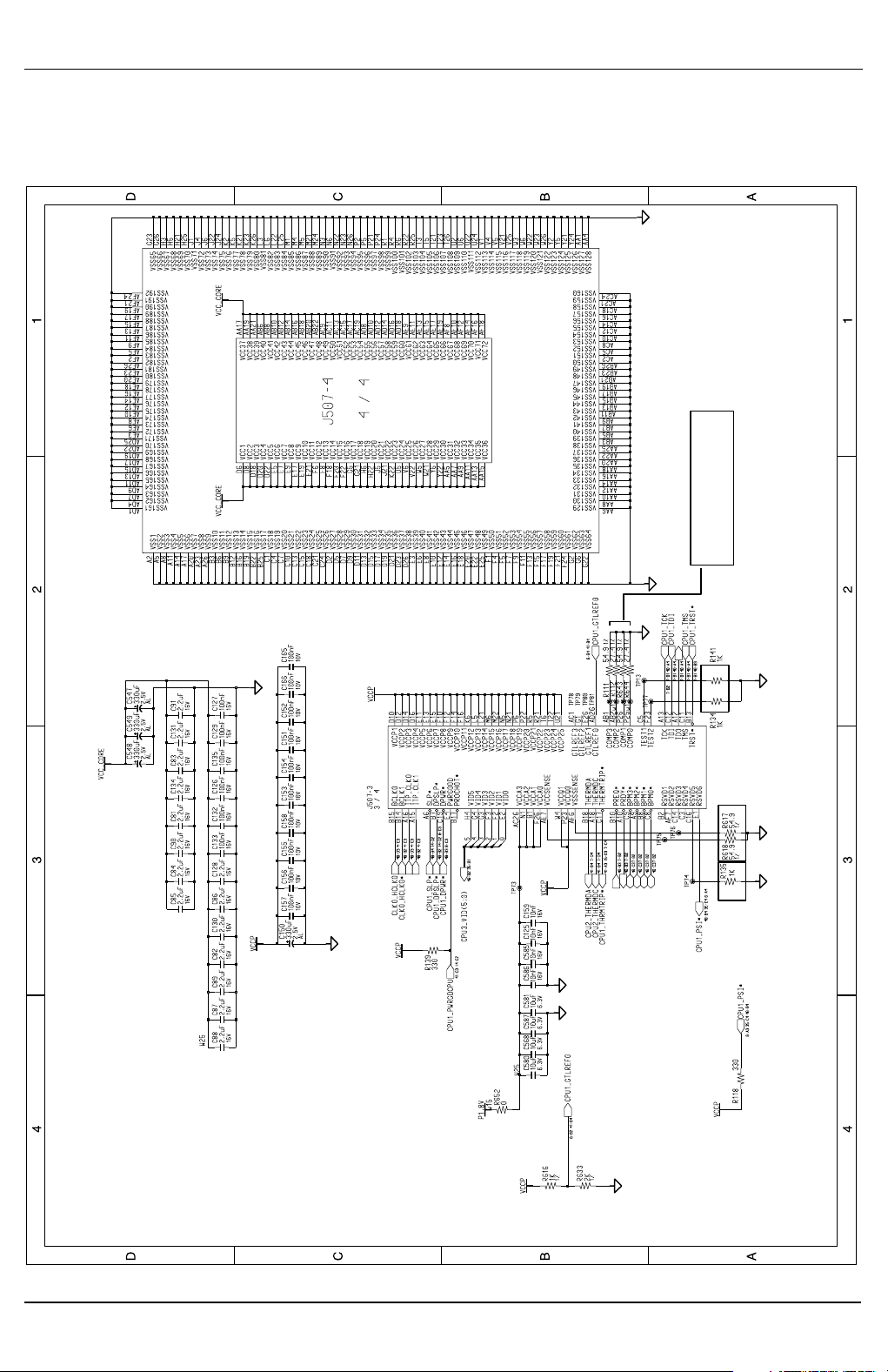
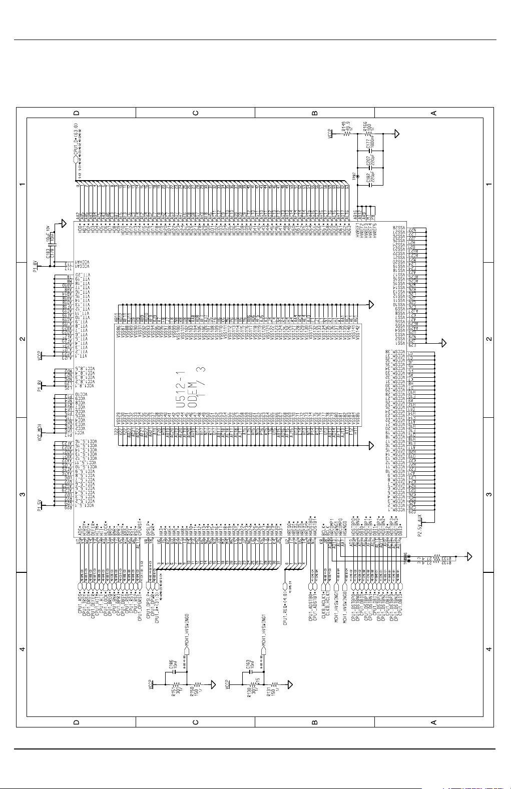
7-1-1(g) Main Board Schematic Sheet 8 of 39(MCH-M)
7 Schematic Diagrams and PCB Silkscreen
7-9X10
> Differential clock length must be 1~2" longer than Strobe signals.
RCVEN Sinal must be routed on the same layer as the memory clocks.
> Differential clock length must be 1~3" longer than Control and Command signals.
DDR Clocks Routing
Value Check?
> SCK/SCK#[3] = SCK/SCK#[4] = SCK/SCK#[5]
DDR Feedback Routing
Place the R,C within 1" of the MCH-M.
MCH output signal via to input signal via = 95mil ~ 105 mil
MCH signal ball to signal Via = Max 40 mil
> SCK/SCK#[0] = SCK/SCK#[1] = SCK/SCK#[2]
7-1-1(h) Main Board Schematic Sheet 9 of 39(MCH-M)
7 Schematic Diagrams and PCB Silkscreen
X107-10
NO STUFF
ST1
NO STUFF
0X
Place near MCH
RSVD1, RSVD2, ETS CHECK ??
Place near AGP
MCH Strap
400 MHz1X
DDR
ST2
X
NO STUFF
1
TEST
40.2 ohm(HeatherCanyon0.9)
7-1-1(i) Main Board Schematic Sheet 10 of 39(MCH-M)
7 Schematic Diagrams and PCB Silkscreen
7-11X10
P/N : 3709-001193 P/N : 3709-001196
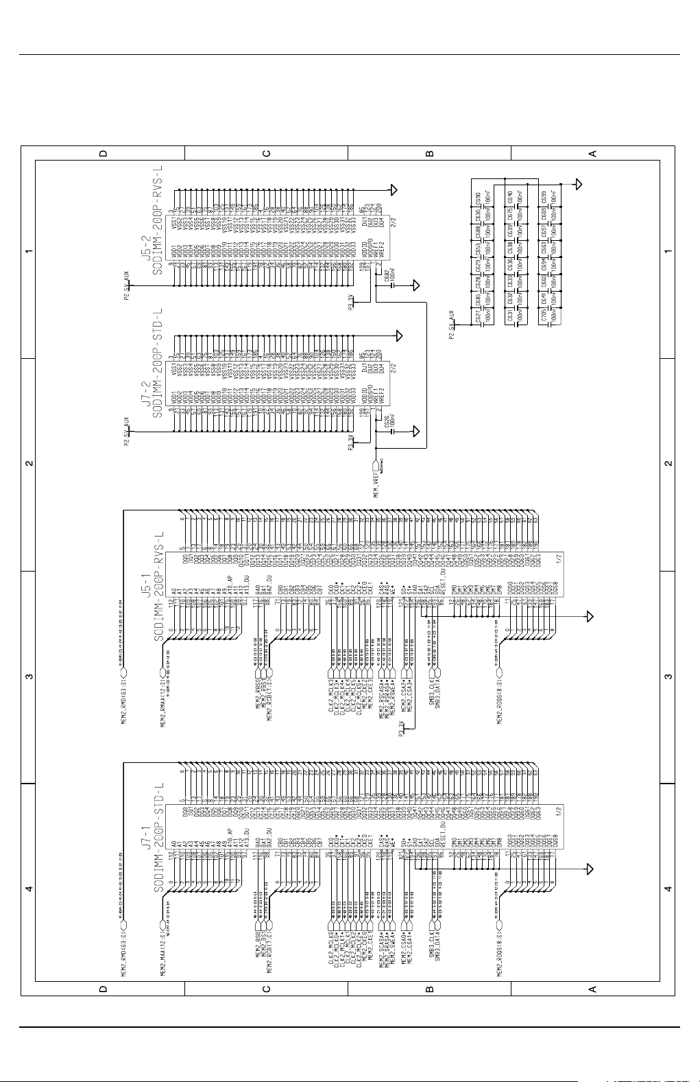
7-1-1(j) Main Board Schematic Sheet 11 of 39(DDR-SODIMM)
7 Schematic Diagrams and PCB Silkscreen
X107-12
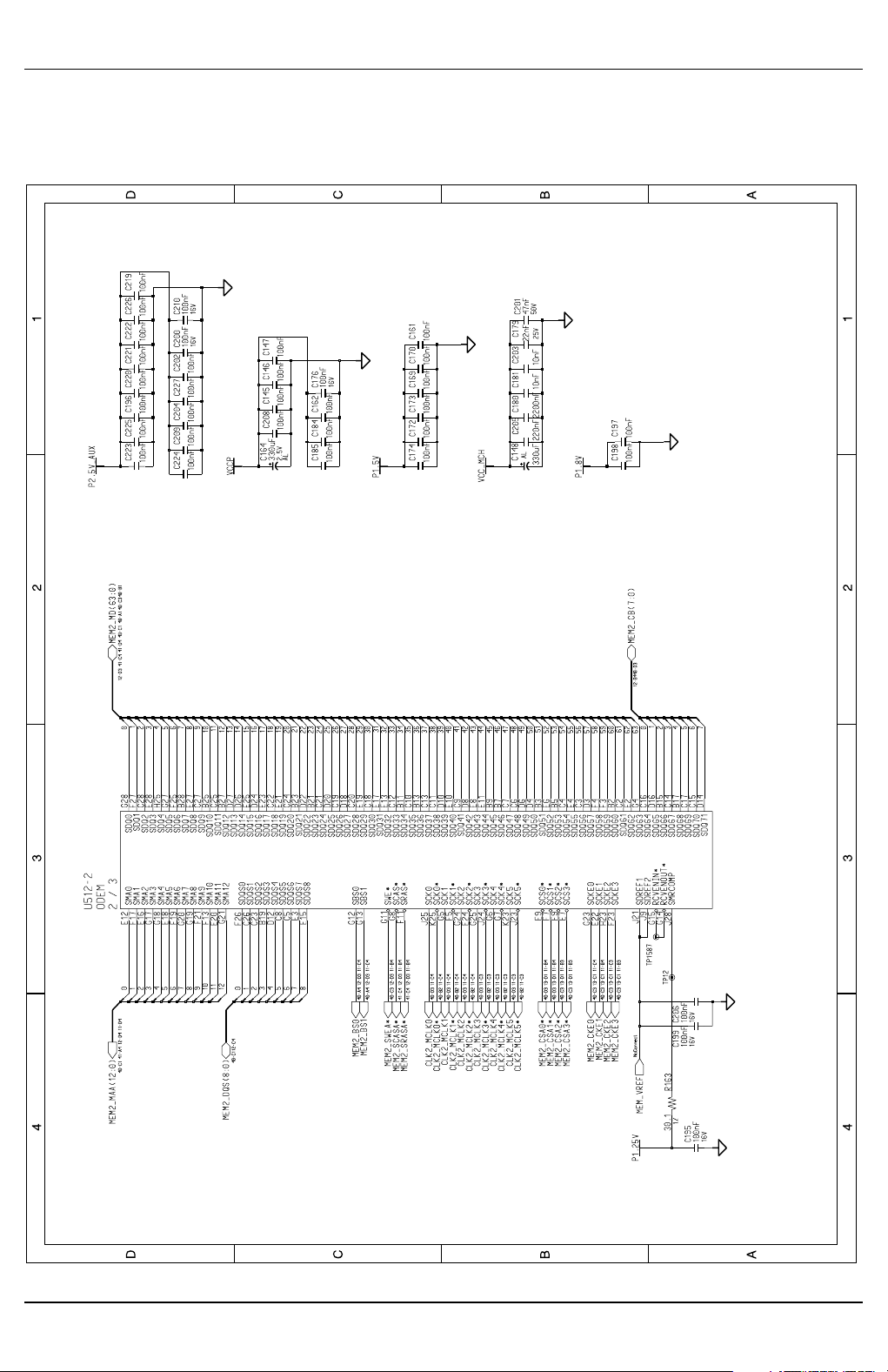
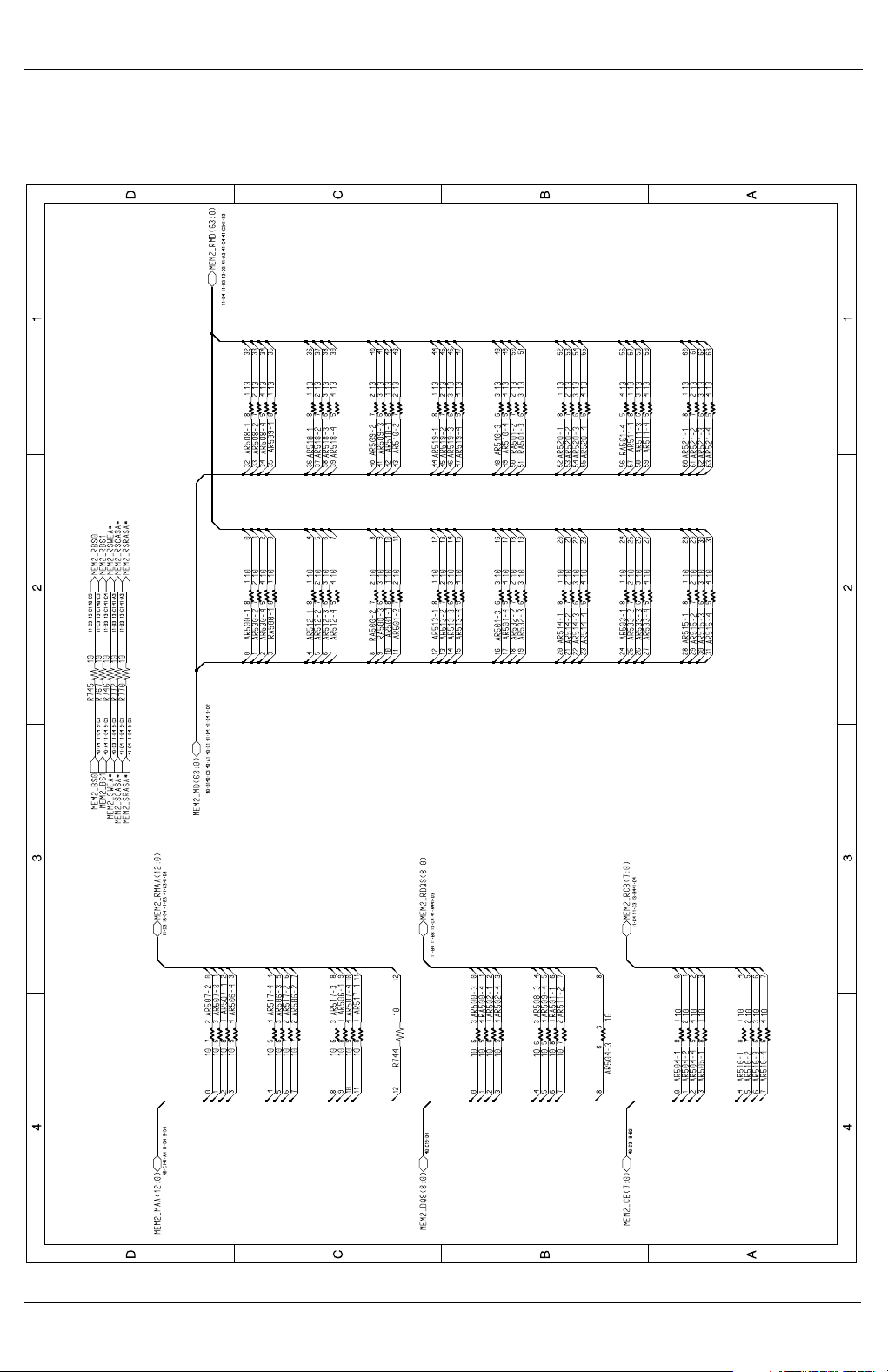
7-1-1(k) Main Board Schematic Sheet 12 of 39(DDR-S Termination)
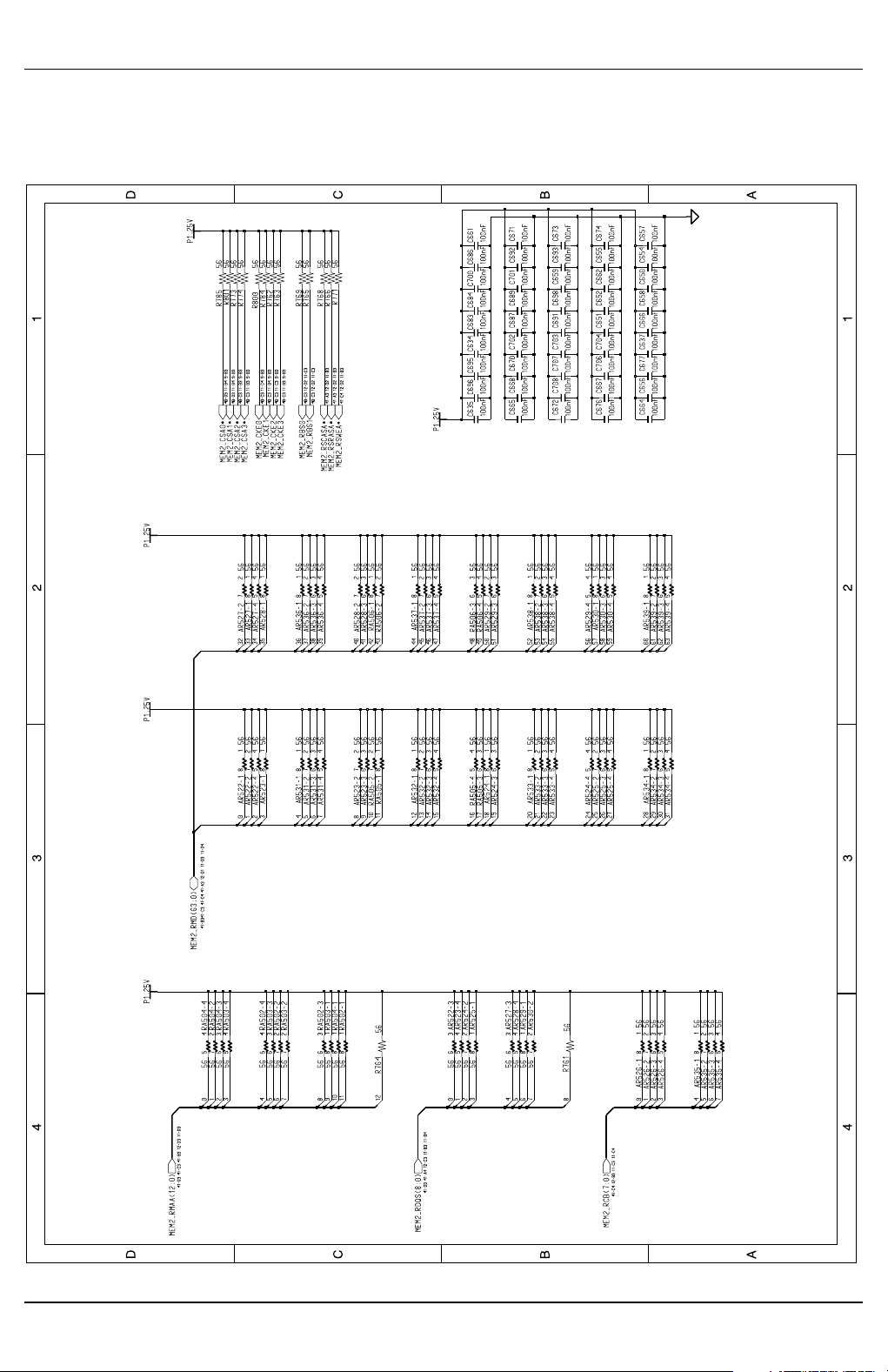
7 Schematic Diagrams and PCB Silkscreen
7-13X10
Place 1 Cap close to every 2 pullup resisters terminated to +V1.25
7-1-1(l) Main Board Schematic Sheet 13 of 39(DDR-P Termination)
7 Schematic Diagrams and PCB Silkscreen
X107-14
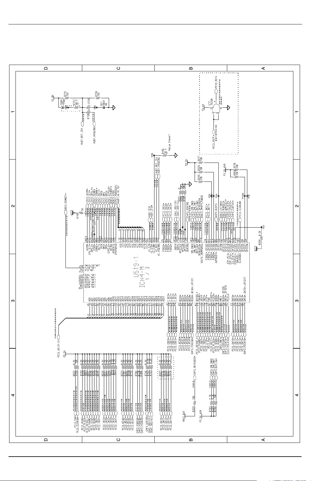
RCOMP R should be 2/3 board impedance
2 inches of ICH4-m. Value check?
Place resistor near ICH4-m
Place series termination within
NO STUFF
Signals must match +/- 0.1" of Strobe signals.
Hub I/F : Route Signal with 5/20 trace/space routing.
PLACE RCOMP Resistor within 0.5" of ICH pad using thick trace
NO STUFF
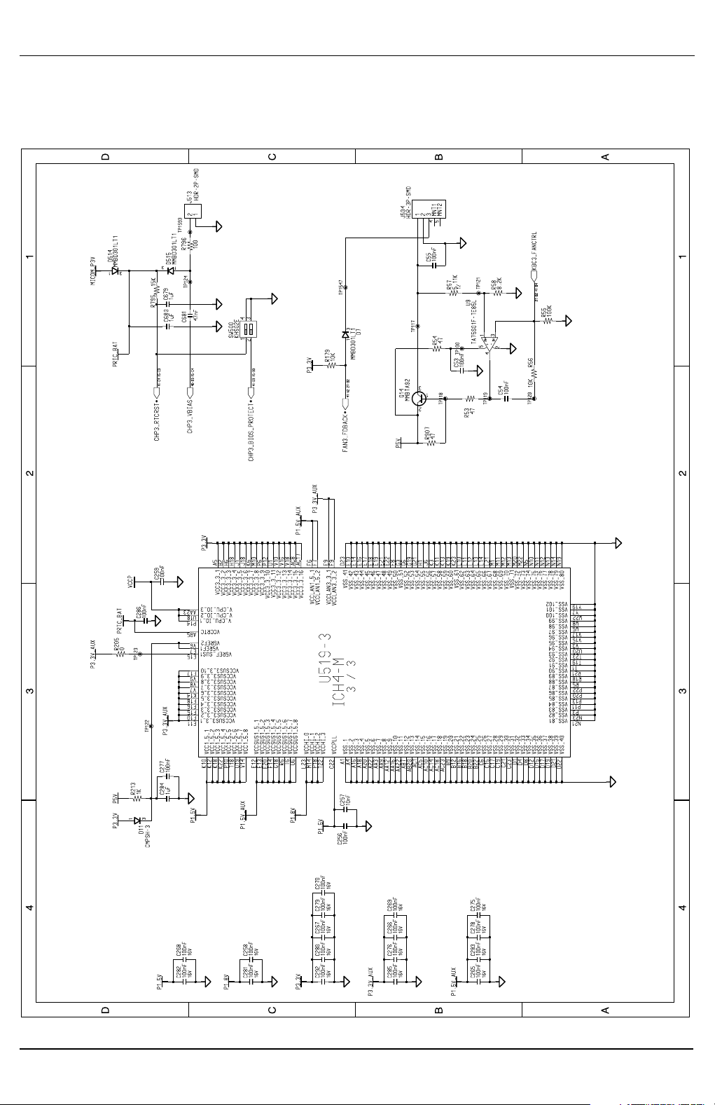
7-1-1(m) Main Board Schematic Sheet 14 of 39(ICH-4)
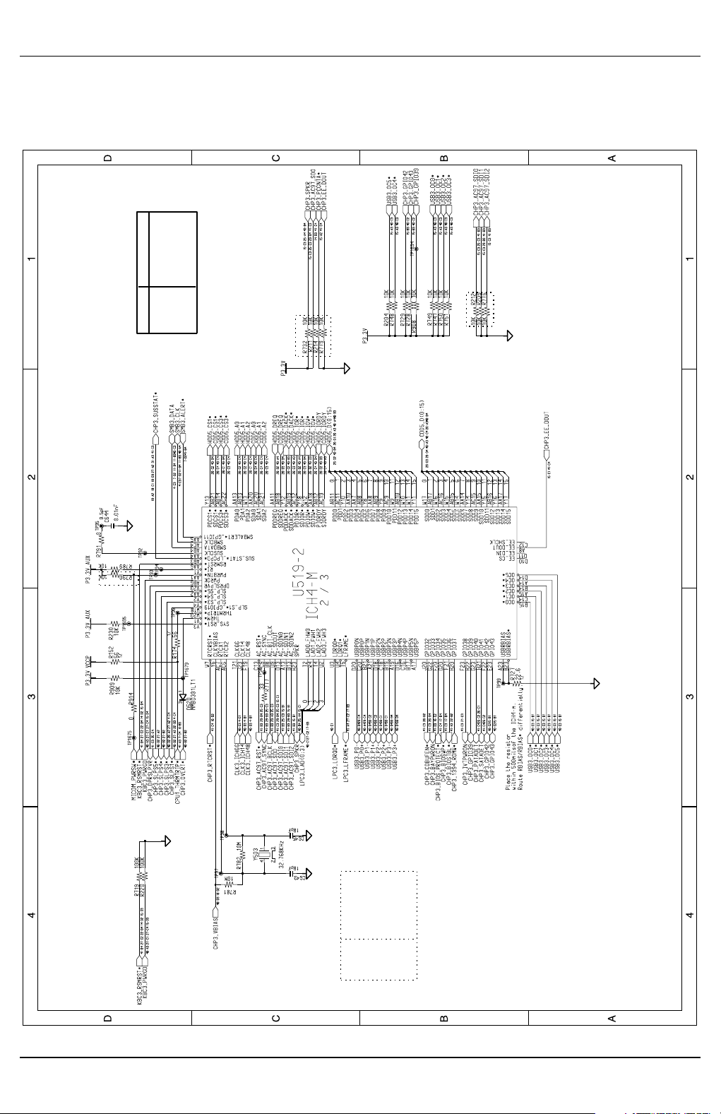
7 Schematic Diagrams and PCB Silkscreen
7-15X10
EEP_DOUT
USB0 Port A
No Reboot
No stuff
No Stuff
Reserved
Secondary CODEC : MODEM
A16 swap override
Function
Primary CODEC : AUDIO
AC97_SDOUT
NO STUFF
Default
USB3 Finger Print
PC/PCI GNTA*
No Stuff
USB1 Port B
USB2 Bluetooth
NO STUFF
No Stuff
ICH_SPKR
Safe Mode
ICH4-m Strapping Options
No Stuff
USB PORT
7-1-1(n) Main Board Schematic Sheet 15 of 39(ICH-4)
7 Schematic Diagrams and PCB Silkscreen
X107-16
0 ~ 5V
0 ~ 3.3V
7-1-1(o) Main Board Schematic Sheet 16 of 39(ICH-4)
7 Schematic Diagrams and PCB Silkscreen
7-17X10
7-1-1(p) Main Board Schematic Sheet 17 of 39(Firmware HUB)
7 Schematic Diagrams and PCB Silkscreen
X107-18
USER(0)
USER(3)
Panel power Good signal
0
Test Option
GPIO(7)
Option
(Geforce4Go 420)
MAP17 232
GPIO(3)
-
Backlight enable
USER(1)
Gfx Core Voltage Switching
GPIO
GPIO(5)
-
Option
-
-
Panel power enable
Hardware suspend
GPIO(1:0)
-
-
USER(2)
Spread spectrum support
GPIO(6)
Panel ID Switch
GPIO(2)
GPIO(4)
VGA3_BLUE
VGA3_C
VGA3_Y
VGA3_VSYNC
VGA3_HSYNC
AGP1_WBF*
AGP1_VREF
AGP1_ST(2)
AGP1_ST(1)
AGP1_ST(0)
AGP1_RBF*
AGP1_PIPE*
AGP1_ADSTB1*
AGP1_ADSTB1
AGP1_ADSTB0*
AGP1_ADSTB0
VGA3_GPIO0
VGA3_SSON
CHP3_SUSSTAT*
VGA3_SSOUT
VGA3_A1-
VGA3_A1+
VGA3_A0-
VGA3_A0+
VGA3_CLK-
VGA3_CLK+
AGP1_GSTOP*
AGP1_GREQ*
AGP1_GPAR
AGP1_GGNT*
AGP1_GFRAME*
AGP1_GDEVSEL*
CLK3_AGP66
AGP1_GCBE*(3)
AGP1_GCBE*(2)
AGP1_GCBE*(1)
AGP1_GCBE*(0)
VGA3_DDCD
VGA3_DDCC
VGA3_GPIO7
CHP3_SUSSTAT*
VGA3_SSON
VGA3_LCDVDDON
VGA3_BKLTON
VGA3_GPIO0
VGA3_RED
VGA3_GREEN
AGP1_GIRDY*
AGP1_GTRDY*
VGA3_VIPD(0)
VGA3_VIPD(1)
VGA3_VIPHAD0
VGA3_VIPHAD1
VGA3_VIPD(0:7)
VGA3_GPIO0
VGA3_GPIO7
CHP3_SUSSTAT*
AGP1_GSTOP*
AGP1_ADSTB1*
AGP1_ADSTB0*
PCI3_RST*
AGP3_BUSY*
CHP3_C3STAT*
PCI3_INTB*
AGP1_GAD(31:0)
VGA3_SSOUT
VGA3_VIPHAD1
VGA3_VIPHAD0
VGA3_A2-
VGA3_A2+
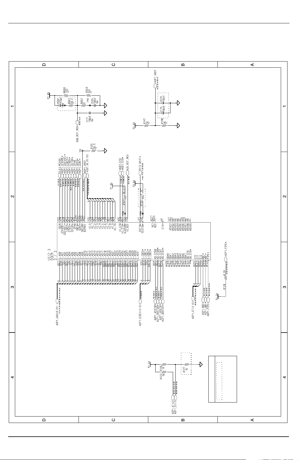
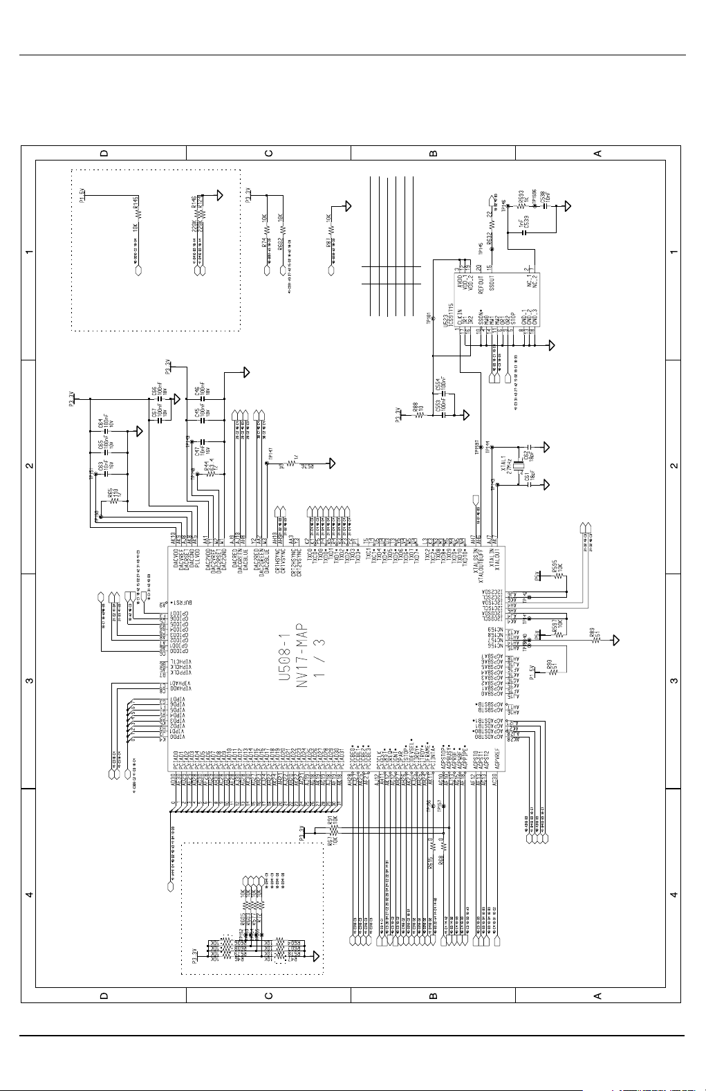
7-1-1(q) Main Board Schematic Sheet 18 of 39(Nvida Map31)
7 Schematic Diagrams and PCB Silkscreen
7-19X10
3.04V
Place bottom, center of GPU
Place on bottom : South-West
Vout = 1.242V x (1+R2/R1)
12k 20k
MIC5205BM5 (Adjustable)
No Stuff
FBVDD (VDDFBC) : 2.0 ~2.5V
Ra
12k 17.4k
Place bottom, close to GPU
11.5k 15k
3.31V
Rb
Vout
2.86V
ADJ
Place close to GPU
Place closest to the GPU
FBVDDQ (VDDFBIO) : 1.8 ~2.5V
Ra
Rb
12k 15k
Place under the GPU
Place on the bottom side under the BGA
Place close to the BGA
Place on bottom : North-West
Place close to GPU
2.79V
VGA3_DVOD(0:11)
VGA3_DVOHSYNC
MSTRAPSEL(3)
MSTRAPSEL(2)
MSTRAPSEL(0)
MSTRAPSEL(1)
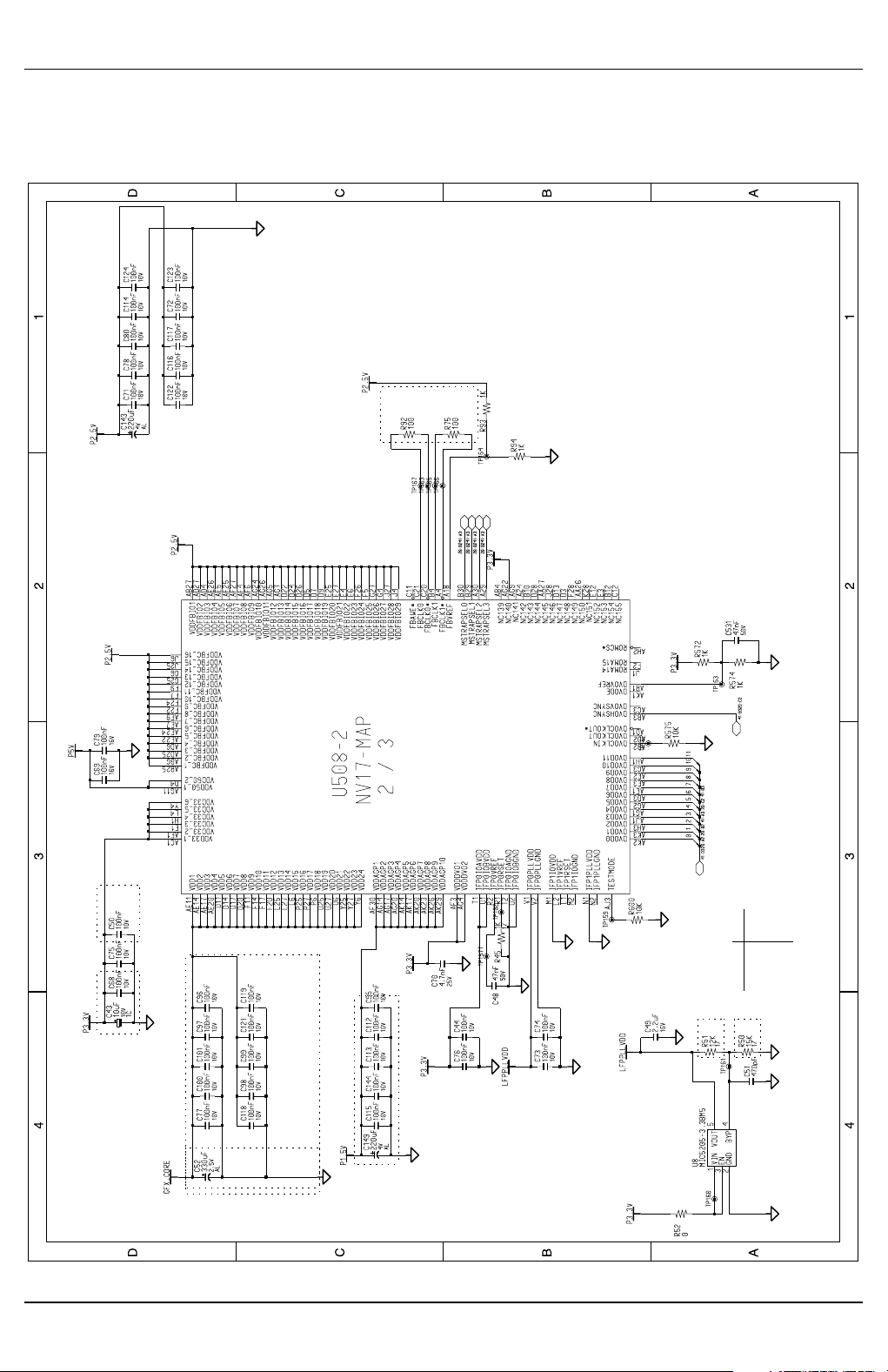
7-1-1(r) Main Board Schematic Sheet 19 of 39(Nvidia Map31)
7 Schematic Diagrams and PCB Silkscreen
X107-20
xx01
DVOD[9]
1101
VIPD(6):DVOD(6)
xxx0
VIPD(7)
Strapping Option
BUS Type ( 1 : AGP mode, 0 : PCI mode )
VGA3_DVOHSYNC
VGA3_VIPD(5)
LOW
LOW
AGP4X ( 0 : 4X enable, 1 : 4X disable )
Crystal ( 10 : 27 MHz )
xx00
HIGH
HIGH
HSYNC,VIPD
xxx1
DVOD[5:2]
DVOD(11)
DVOD(1)
ROM Type ( 00 : Parallel )
RAM Cfg ( 1101 : 4Mx32 DDR SDRAM )
0110
AGP Fastwrite ( 0 : Enable, 1 : Disable )
xxx0
Sub Vendor ( 0 : System BIOS, 1: Adapter BIOS )
DVOD(0)
xxx1
PCI_DEV_ID ( 0110 : NV17-MAP)
DVOD[8:7]
CKE
TV Mode ( 01 : NTSC )
VIPD(2):DVOD(10)
PCI_AD_Swap ( 1 : Normal, 0 : Reverse )
64MB
VGA3_VIPD(3)
VGA3_VIPD(4) LOW
LOW
xxx0
HIGH
HIGH
32MB
xx10
VGA3_DVOD(1)
VGA3_DVOD(0)
VGA3_DVOD(9)
VGA3_DVOD(8)
VGA3_DVOD(7)
VGA3_DVOD(11)
VGA3_VIPD(5)
VGA3_VIPD(3)
VGA3_DVOD(6)
VGA3_DVOD(10)
VGA3_VIPD(2)
VGA3_VIPD(6)
VGA3_VIPD(4)
VGA3_DVOHSYNC
VGA3_VIPD(7)
VGA3_DVOD(3)
VGA3_DVOD(5)
VGA3_DVOD(2)
MSTRAPSEL(0)
MSTRAPSEL(1)
VGA3_DVOD(4)
MSTRAPSEL(2)
MSTRAPSEL(3)
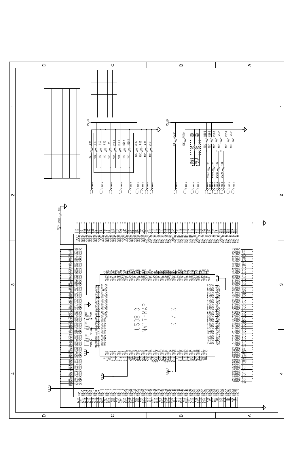
7-1-1(s) Main Board Schematic Sheet 20 of 39(Nvidia Map31)
7 Schematic Diagrams and PCB Silkscreen
7-21X10
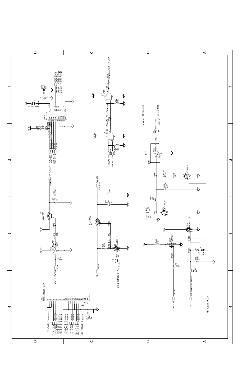
LCD CONNECTOR
7-1-1(t) Main Board Schematic Sheet 21 of 39(LCD_Connector)
7 Schematic Diagrams and PCB Silkscreen
X107-22
No Stuff
Terminators -> Close to R5C590
682097
3) TPBIAS0, TPAP0, TPAN0, TPBP0, and TPBN0
Apply Guard Grounding to Following Signals
4) TPBIAS1, TPAP1, TPAN1, TPBP1, and TPBN1
--> Place XTAL near R5C590 as close as possible
Max.:10mm, Typ: 5mm
* GUARD GROUND *
Should be compact circuit area
1) Xtal for X1/X0 (Y1 24.576MHz) and its capacitors
2) FIL0, REXT and VREF
For Internal Analog
Capacitors should be located near R5C590 chipset
PCI3_PAR
PCI3_DEVSEL*
PCI3_FRAME*
PCI3_GNT0*
PCI3_IRDY*
PCI3_PERR*
PCI3_REQ0*
PCI3_SERR*
PCI3_STOP*
PCI3_TRDY*
PCI3_INTA*
PCI3_INTB*
PCI3_INTC*
PCI3_AD(19)
PCI3_RST*
CHP3_PME*
PCI3_AD(0:31)
CBS3_SPKR
PCI3_CBE0*
CLK3_PCLKCB
KBC3_PWRGD
PCI3_CLKRUN*
PCI3_CBE1*
PCI3_CBE2*
PCI3_CBE3*
7-1-1(u) Main Board Schematic Sheet 22 of 39(Cardbus & 1394)
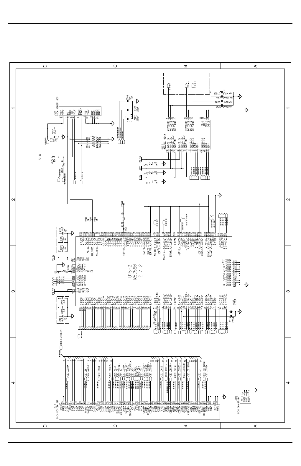
7 Schematic Diagrams and PCB Silkscreen
7-23X10
2) A_MS_SCLK (J20)
Capacitors should be located
1) CB3_CCLK (A1)
is removed
near R5C590
MemoryStick Socket
Switched Power Output Group
CARDBUS SOCKET CONNECTOR
CA3_VPP
Socket Frame
No Stuffing
Capacitors should be located
Apply Shiled Grounding to Following Signals;
* SHIELD GROUND *
near R5C590
CB3_BVPP1
CB3_BVCC3*
CB3_BVCC5*
CB3_VCC
CA3_VCC
CB12_VPP
CB3_BVPP0
CB3_AVCC3*
CB3_AVPP1
CB3_AVPP0
CB3_AVCC5*
CB3_B4
CB3_J1
CB3_B8
CB3_D5
A_CD1*
CB3_AVCC5*
CB3_AVPP1
CB3_AVPP0
CB3_AVCC3*
MS_RFU7
A_CD1*
A_CD2*
A_MC_CD*
A_CD2*
MS_SCLK
CB3_BVPP1
CB3_BVPP0
CB3_BVCC3*
CB3_BVCC5*
A_MC_CD*
MS_RFU7
MS_SCLK
CA3_VCC
CB3_CAD(0:31)
CB3_CCLK
CB3_CVS2
CB3_CVS1
CB3_CTRDY*
CB3_CSTOP*
CB3_CPERR*
CB3_CPAR
CB3_CIRDY*
CB3_CGNT*
CB3_CFRAME*
CB3_CDEVSEL*
CB3_CCLKRUN*
CB3_CSTSCHG
CB3_CSERR*
CB3_CREQ*
CB3_CRST*
CB3_CINT*
CB3_CCD2*
CB3_CCD1*
CB3_CAUDIO
CB3_CCBE3*
CB3_CCBE2*
CB3_CCBE1*
CB3_CCBE0*
CB3_CRST*
A_CD2*
A_CD1*
7-1-1(v) Main Board Schematic Sheet 23 of 39(Cardbus Socket)
7 Schematic Diagrams and PCB Silkscreen
X107-24
MINIPCI
5.3mm
7-1-1(w) Main Board Schematic Sheet 24 of 39(Mini PCI)
7 Schematic Diagrams and PCB Silkscreen
7-25X10
NO STUFF
NO STUFF
682097
Place near HP & MIC conn audio ground partition
Place each caps near the pinof CS4299
NO STUFF
HP_IN
AUD5_MIC_CODEC
LID3_SWITCH*
AUD5_SPK_L-
AUD5_SPK_R-
MDC_AUDIN AUD3_PHONE
7-1-1(x) Main Board Schematic Sheet 25 of 39(Audio Codec & AMP)
7 Schematic Diagrams and PCB Silkscreen
X107-26
LOW : ATA66/100
NO STUFF
HIGH : ATA33
No Stuff
No Stuff
7-1-1(y) Main Board Schematic Sheet 26 of 39(Bay Connector)
7 Schematic Diagrams and PCB Silkscreen
7-27X10
TXD
72
SK : 3704-001155
109
NC
108
IC : 0903-001231
NO STUFF
RXD
73
144
NO STUFF
NC
36
1
682081
37
7-1-1(z) Main Board Schematic Sheet 27 of 39(MICOM)
7 Schematic Diagrams and PCB Silkscreen
X107-28
smbus mode
NO STUFF
No Stuff
standard feature
16k EEPROM
Place these near VSSX4 PIN as you can
7-1-1(aa) Main Board Schematic Sheet 28 of 39(3COM LAN & MDC)
7 Schematic Diagrams and PCB Silkscreen
7-29X10
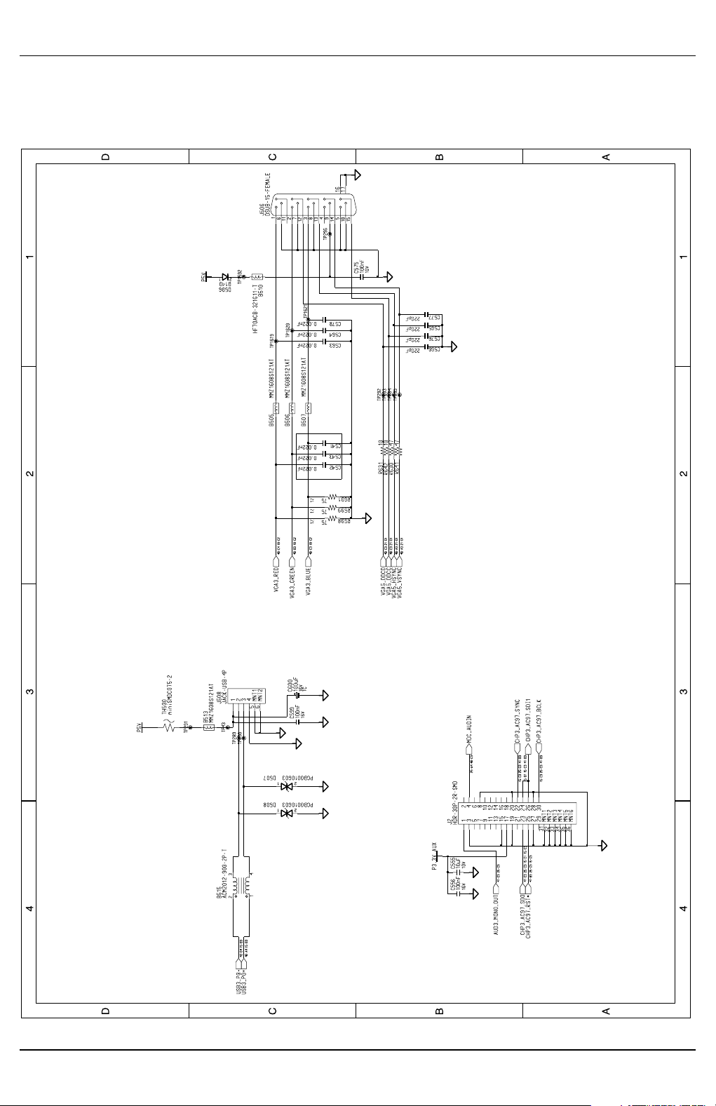
CRT CONNECTOR
MDC connector
NO STUFF
change it 1005 type LATER
7-1-1(bb) Main Board Schematic Sheet 29 of 39(USB Connector)
7 Schematic Diagrams and PCB Silkscreen
X107-30
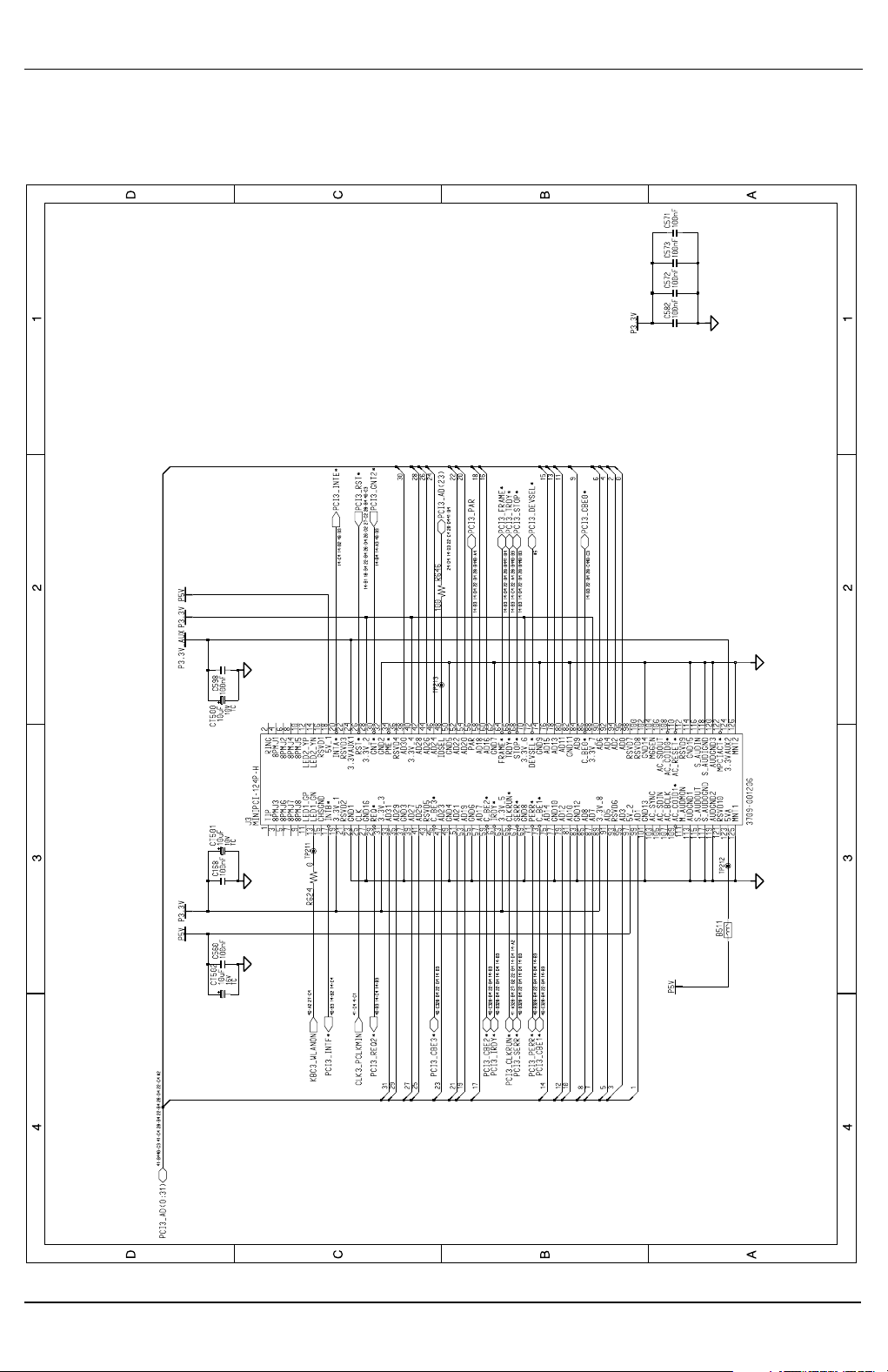
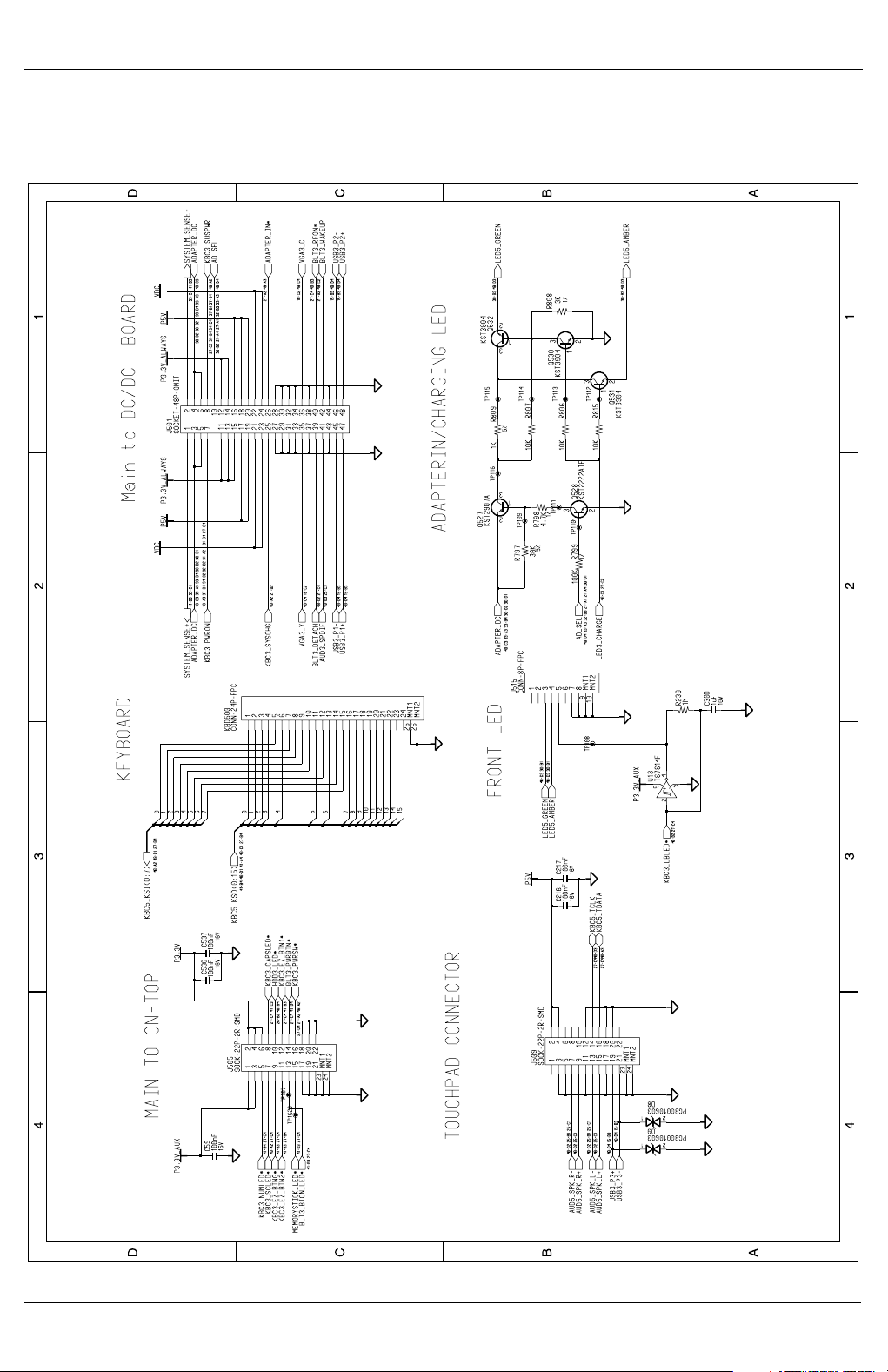
7-1-1(cc) Main Board Schematic Sheet 30 of 39(B’D TO B’D Connector)
 Loading...