

Samsung LA32R81BD, LA40R81BD Schematic
TFT-LCD TV
Chassis GBP32CAU
GBP40CAU
Model LA32R81BD
LA40R81BD
Manual
SERVICE
TFT-LCD TV Fashion Feature
- Luxurious Slim Design
- Supreme Picture Quality
- Supreme Sound Quality
- Supreme Convenience Quality
- Convenience for Users
- iDTV

ii
Copyright
ⓒ 2007 by Samsung Electronics Co., Ltd.
All rights reserved.
This manual may not, in whole or in part, be copied,
photocopied, reproduced, translated, or converted to any
electronic or machine readable form without prior
written permission of Samsung Electronics Co., Ltd.
LA32R81BD/LA40R81BD Service Manual
First edition March 2007.
Printed in Korea.
Trademarks
Samsung is the registered trademark of Samsung
Electronics Co., Ltd.
LA32R81BD/LA40R81BD Service Manual and
Macmaster Cable Adapter are trademarks of Samsung
Electronics Co., Ltd.
Macintosh and Power Macintosh are trademarks of
Apple Computer, Inc.
All other trademarks are the property of their respective
owners.

Contents
11. Precautions
………………………………………………………………………………………………………………………………………
11-1
1-1 Safety Precautions ……………………………………………………………………………………………………………………… 1-1
1-2 Servicing Precautions …………………………………………………………………………………………………………………… 1-2
1-3 Static Electricity Precautions …………………………………………………………………………………………………………… 1-2
1-4 Installation Precautions…………………………………………………………………………………………………………………… 1-3
2
2. Product specifications
…………………………………………………………………………………………………………………………
22-1
2-1 Fashion Feature…………………………………………………………………………………………………………………………… 2-1
2-2 LA32R81BD Specifications ……………………………………………………………………………………………………………… 2-2
2-3 LA32R81BD Specifications ……………………………………………………………………………………………………………… 2-3
2-4 Spec Comparison ………………………………………………………………………………………………………………………… 2-4
2-5 Option Specification ……………………………………………………………………………………………………………………… 2-5
3
3. Alignments and Adjustments
…………………………………………………………………………………………………………………
3
3-1
3-1 Service Instruction ……………………………………………………………………………………………………………………… 3-1
3-2 How to Access Service Mode …………………………………………………………………………………………………………… 3-2
3-3 Factory Data ……………………………………………………………………………………………………………………………… 3-3
3-4 Service Adjustment ……………………………………………………………………………………………………………………… 3-11
3-5 Software Upgrade ……………………………………………………………………………………………………………………… 3-14
4
4. Troubleshooting
………………………………………………………………………………………………………………………………
44-1
4-1 First Checklist for Troubleshooting ………………………………………………………………………………………………………4-1
4-2 Checkpoints by Error Mode ……………………………………………………………………………………………………………… 4-2
5
5. Exploded View and Parts List
…………………………………………………………………………………………………………………
55-1
5-1 LA32R81BDX Exploded View ……………………………………………………………………………………………………………5-1
5-2 LA32R81BDX Parts list…………………………………………………………………………………………………………………… 5-2
5-3 LA40R81BDX Exploded View ……………………………………………………………………………………………………………5-3
5-4 LA40R81BDX Parts list…………………………………………………………………………………………………………………… 5-4
6
6. Electrical Parts List
……………………………………………………………………………………………………………………………
66-1
6-1 LA32R81BD Parts List …………………………………………………………………………………………………………………… 6-1
6-2 LA40R81BD Parts List ………………………………………………………………………………………………………………… 6-33
7
7. Block Diagram
…………………………………………………………………………………………………………………………………
77-1
8. WWiring Diagram
…………………………………………………………………………………………………………………………………
88-1
8-1 Wiring Diagram ……………………………………………………………………………………………………………………………8-1
8-2 Main Board Layout ……………………………………………………………………………………………………………………… 8-2
8-3 PIN characteristic ………………………………………………………………………………………………………………………… 8-3
8-4 Connector Location and PCB outline figure …………………………………………………………………………………………… 8-6
99. Schematic Diagrams
……………………………………………………………………………………………………………………………
99-1

Contents
110. Operating Instructions and Installation
………………………………………………………………………………………………………
110-1
10-1 Front …………………………………………………………………………………………………………………………………… 10-1
10-2 Viewing the Connection Panel ……………………………………………………………………………………………………… 10-2
10-3 Remote control ………………………………………………………………………………………………………………………… 10-4
10-4 Installation the Stand ………………………………………………………………………………………………………………… 10-5
10-5 Installing the Wall Mount Kit ………………………………………………………………………………………………………… 10-5
1
11. Disassembly and Reassembly
………………………………………………………………………………………………………………
111-1
11-1 Disassembly …………………………………………………………………………………………………………………………… 11-1
11-2 Reassembly …………………………………………………………………………………………………………………………… 11-5
1
12. PCB Diagram
…………………………………………………………………………………………………………………………………
112-1
12-1 Main PCB Diagram …………………………………………………………………………………………………………………… 12-1
113. Circuit Descriptions
……………………………………………………………………………………………………………………………
113-1
13-1 Main Signal Description ……………………………………………………………………………………………………………… 13-1
13-2 DTV Signal Description ……………………………………………………………………………………………………………… 13-2
13-3 RF/DTV Tuner (DNOS403MH261B(S)) SPEC. …………………………………………………………………………………… 13-3
13-4 DTV MAIN ChipSet …………………………………………………………………………………………………………………… 13-9
1
14. Reference Infomation
………………………………………………………………………………………………………………………
114-1
14-1 Technical Terms ……………………………………………………………………………………………………………………… 14-1
14-2 Pin Assignments ……………………………………………………………………………………………………………………… 14-4
14-3 Timing Chart …………………………………………………………………………………………………………………………… 14-7
14-4 Panel Description …………………………………………………………………………………………………………………… 14-11
Samsung Electronics Co.,Ltd.
416, Maetan-3Dong, Yeongtong-Gu, Suwon City,
Gyeonggi-Do, Korea, 443-742
Printed in Korea
P/N : BN82-00200A-00
URL : http://itself.sec.samsung.co.kr/
- This Service Manual is a property of
Samsung Electronics Co., Ltd.
Any unauthorized use of Manual can be
punished under applicable International
and/or domestic law.

3 Alignments and Adjustments
3-1
3 Alignments and Adjustments
3-1 Ser vice Instr uction
1. Usually, a color TV-VCR needs only slight touch-up adjustment upon installation.
Check the basic characteristics such as height, horizontal and vertical sync.
2. Use the specified test equipment or its equivalent.
3. Correct impedance matching is essential.
4. Avoid overload. Excessive signal from a sweep generator might overload the front-end
of the TV. When inserting signal markers, do not allow the marker generator to distort
test result.
5. Connect the TV only to an AC power source with voltage and frequency as specified on
the backcover nameplate.
6. Do not attempt to connect or disconnect any wire while the TV is turned on. Make sure
that the power cord is disconnected before replacing any parts.
7. To protect aganist shock hazard, use an isolation transform.
3 Alignments and Adjustments
3-2
3-2 How to Access Service Mode
3-2-1 Entering Factory Mode
1. To enter "Service Mode" Press the remote -control keys in this sequence :
- If you do not have Factory remote - control
- If you have Factory remote - control
- The buttons are active in the service mode.
1. Remote - Control Key : Power, Arrow Up, Arrow Down, Arrow Left
Arrow Right, Menu, Enter, Number Key(0~9)
2. Function - Control Key : Power, CH +, CH -, VOL +, VOL -,
Menu, TV/VIDEO(Enter)
3-2-2 Panel Check
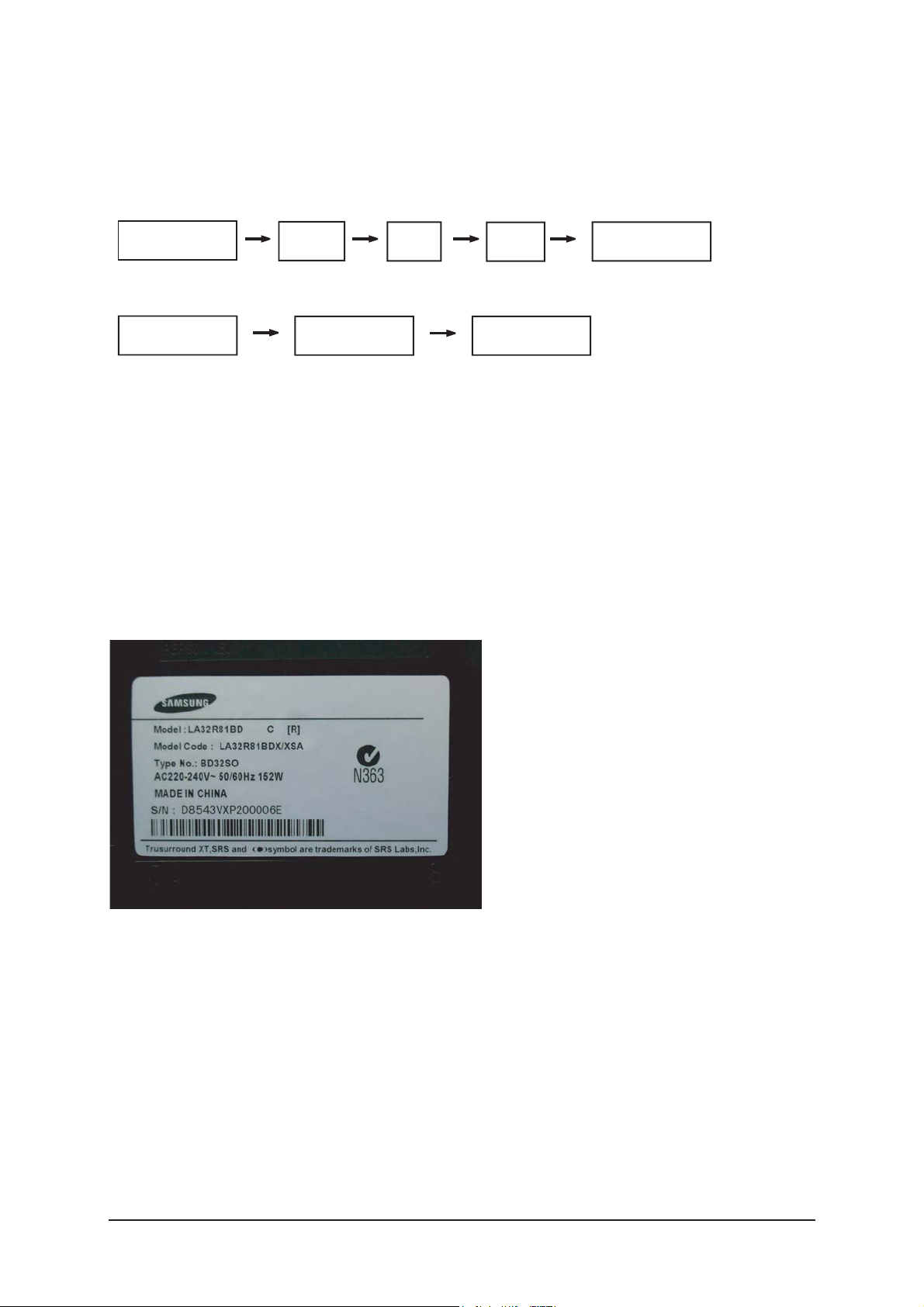
You have to check Panel Maker Because of different adjustments as follows.
First of all, Check the label rating!
1) Label Rating File
- LCD PANEL MARK A:ACER(AUO) S : SEC C : CMO * If not printed you could consider S(sec) panel mark.
2) If Panel Mark is "A", Set the factory mode indicating as follows.
* Option Byte
1. Inch Option 32"
2. Gamma 32"AUO
3. Panel Option AUO
Others are same shown below.
Power OFF
INFO
MENU
MUTE
Power ON
PICTURE ON
DISPLAY
FACTORY

3 Alignments and Adjustments
3-3
3-3 Factory Data
Panel On Time(Hour) XXXXX
BORDEAUX+ XXXX
1. Calibration
2. Option Table (Service)
3. White Balance
4. SVP-UX
5. Option Block
6. SGTV 5810/NTP3000
7. Y/C Delay
8. Adjust
9. I2C Check
10.W/B Movie
11.Checksum
12.Reset
13 Spread Spectrum
T-BDPMPAUD-XXXX
T-BDPMPEUS-XXXX
BORD2_CALLA_TR-XXXX
Boot Merge : XX
Month /Day /Year
Hour /Min. /Sec.
1. Calibration :W/B Calibration
1) AV Calibration Success
2) DTV Calibration Success
3) PC Calibration Success
4) HDMI Calibration Success
3 Alignments and Adjustments
3-4
No
Item
1
2
3
4
5
6
7
8
9
10
11
12
13
14
15
16
17
18
19
20
21
22
23
24
25
26
27
28
29
Ready
Inch Option
Panel Vender
Panel Type
Model Option
PDP Filter
Anynet +
Light Effect
WM Calib
Auto Power
Nordic
LNA Menu
TTX On/Off
TTX List
Carrier Mute
High Devi.
VOL.Curve
HDMI HotPlug
HDMI Clk Ctrl
HDMI HP Dly
Hotel Option
Shop Mode
Color Space
PC Ident
Language
Ch.Table
TTX Group
IDTVCountry
PDP Group
OFF
32"
CMO_INT
32"CMO
Bord Plus
50" EU MRT
ON
OFF
OFF
ON
OFF
ON
ON
Flof
OFF
OFF
Small
1
1
9
OFF
ON
ON
English
TSED
Auto
Australia
C5E_DMA
Range
2. Option Table XXXX XXXX
3 Alignments and Adjustments
3-5
No
Item Range
1
2
3
4
5
6
7
8
Sub Bright.
R-Offset
G-Offset
B-Offset
Sub Cont.
R-Gain
G-Gain
B-Gain
128
134
128
123
140
098
128
138
4. SVP-PX
1) ComB Filter
2) Sharpness
No
1
Item
Y-Filter
Range
00H
No
1
2
3
4
5
6
7
8
9
10
11
Item
H2Gain
H4Gain
V2Gain
V4Gain
Sr2Gain
Sr4Gain
Sl2Gain
Sl4Gain
Peakth1
Peakth2
Peskth3
Range
00H~FFH
00H~FFH
00H~FFH
00H~FFH
00H~FFH
00H~FFH
00H~FFH
00H~FFH
00H~FFH
00H~FFH
00H~FFH
RF
08H
08H
10H
10H
00H
00H
00H
00H
03H
2FH
42H
AV
08H
08H
10H
10H
00H
00H
00H
00H
03H
2FH
42H
Comp
06H
06H
10H
10H
00H
00H
00H
00H
03H
2FH
46H
PC
01H
01H
02H
02H
00H
00H
00H
00H
06H
2FH
40H
HDMI
0AH
0AH
10H
10H
00H
00H
00H
00H
03H
2FH
50H
3. White Balance :Adjustment W/B (0-255)
3) NR
No
1
2
3
4
Item
Y_NR_OFF
C_NR_OFF
Y_NR_ON
C_NR_ON
Range
00H~FFH (Y_NR_OFF)
00H~FFH (C_NR_OFF)
00H~FFH (Y_NR_ON)
00H~FFH (C_NR_ON)
00H
00H
00H
00H
3 Alignments and Adjustments
3-6
4) RGB Calibration
5) ADC Calibration
6) Caliration Target
No
Item Range
1
2
3
4
5
6
R-Offset
G-Offset
B-Offset
R-Gain
G-Gain
B-Gan
00H~FFH
00H~FFH
00H~FFH
00H~FFH
00H~FFH
00H~FFH
33H
33H
33H
A8H
A8H
A8H
40H
40H
40H
92H
92H
91H
33H
33H
33H
A8H
A8H
A8H
41H
41H
41H
91H
91H
91H
RF/AV Component PC
HDMI
No
Item Range
1
2
3
4
AV ADC
COMP ADC
PC ADC
ALL RGB
00H~FFH
00H~FFH
00H~FFH
00H~FFH
10H
10H
10H
01H
DCH
EBH
DCH
EBH
02H
02H
04H
0AH
low high Delta
No
Item Range
1
2
3
4
5
6
7
8
9
10
11
12
13
TCD3 Contrast
TCD3 Brightness
TCD3 CR
TCD3 CB
TCD3 Delay
Analog Y Offset
Analog PB Offset
Analog PR Offset
Analog Y Gain
Analog PB Gain
Analog PR Gain
Black Level
Svp Brightness
00H~FFH
00H~FFH
00H~FFH
00H~FFH
00H~FFH
00H~FFH
00H~FFH
00H~FFH
00H~FFH
00H~FFH
00H~FFH
00H~FFH
00H~FFH
7AH
2AH
80H
80H
00H
40H
80H
80H
D6H
80H
80H
00H
00H
78H
20H
80H
80H
00H
3EH
80H
80H
CEH
CEH
CEH
00H
00H
78H
20H
80H
80H
00H
44H
44H
43H
B2H
ADH
ACH
00H
00H
78H
20H
80H
80H
00H
40H
80H
80H
80H
80H
80H
00H
00H
RF/AV Component PC
HDMI
5. Option Block
7) Color Management
1) FRC(Micronas)
2) FRC-Samsung
No
Item Range
1
2
3
4
Skin Direction
Skin Enhance
Green Stretch
Blue Stretch
Reddish/Yellowish
00H~FFH
00H~FFH
00H~FFH
Reddish
00H
00H
00H
3 Alignments and Adjustments
3-7
3 Alignments and Adjustments
1
2
3
4
5
6
7
8
9
10
11
12
13
14
15
16
17
18
19
20
21
22
23
24
25
26
Pattern Select
BS-On
B-Slope Gain
B-Tilt Min
B-Tilt Max
B-Tilt Slope
LFunc-Basis
Hfunc-Basis
Mean-Offset1
Mean Offset2
Mean Slope
Input Offset
Input Gain
ACR Offset
ACR Th1
ARC Th2
Skin Enable
Skin Tu
Skin Tv
M Skin Tu
M Skin TV
Sub Color
M-Au-Sub Color
M-Wi-Sub Color
MW-Skin-Tu
MW-Skin-Tv
000
001
070
020
120
128
075
090
050
220
093
128
128
010
010
110
001
140
140
128
128
138
128
128
128
128
0
1
34
20
120
128
30
30
20
120
56
128
128
15
30
130
1
165
140
128
128
115
128
128
128
128
0
1
44
20
120
128
20
40
100
200
56
128
128
15
30
130
1
165
140
128
128
128
128
128
128
128
0
1
44
20
120
128
20
40
100
200
56
128
128
15
30
130
1
165
140
128
128
128
128
128
128
128
3) FBE2
No Item Range
0
1
64
20
120
128
55
65
75
225
85
128
128
15
30
130
1
165
128
128
128
150
128
128
128
128
HDMI
0
1
64
20
120
128
75
88
75
225
85
128
128
15
30
130
1
128
128
128
128
143
128
128
128
128
DTV
0
1
64
20
120
128
75
88
75
225
85
128
128
15
30
130
1
128
128
128
128
143
128
128
128
128
DTVRF
AV/
S-VIDEO
COMP
(480i/576i)
0
1
64
20
120
128
40
40
75
155
45
128
128
15
30
130
1
150
140
128
128
135
128
128
128
128
COMP
(480p/576p)
0
1
64
20
120
128
70
75
75
225
85
128
128
15
30
130
1
165
128
128
128
140
128
128
128
128
COMP
(720p/1080i/1080p)
3 Alignments and Adjustments
3-8
4) PDP Logic
No
Item Range
1
2
3
4
5
6
7
8
9
10
11
12
13
Pattern Srlect
Data updata
Data Type
CDC Sw
CDC Strengh Th
BRE Sw
FRC Repeat Mode
FRC CBG Mark On
ERC Bypass
Panel Type
Panel Inch
Panel Version
Logic Sw Version
0~63
ON/OFF
42"EU MRT/42"EU MESH/......
ON/OFF
0~31
ON/OFF
ON/OFF
0~15
ON/OFF
-
-
-
-
0
OFF
42"EU MRT
OFF
0
OFF
OFF
0
OFF
0H
SD
0H 0H 0H
6. SGTV5810/NTP3000
No
Item Range
1
2
3
4
5
6
7
ID Tone Shift
ID Tone Thresh
Demod Prescaler
Master Volume
PWM Modulation
DRC Threshold
Speaker EQ
1H~FH
00H~FFH
00H~20H
00H~30H
80H~F2H
00H~7FH
ON/OFF
01H
7FH
0EH
0FH
F2H
0FH
0FF
7. YC Delay
No
Item Range
1
2
3
4
5
6
7
8
9
10
11
12
13
RF PAL-B/G
RF PAL - D/K
RF PAL - I
RF SECAM - B/G
RF SECAM - D/K
RF SECAM -L/L'
RF NTSC 3.58
RF NTSC 4.43
AV PAL
AV SECAM
AV NTSC 3.58
AV NTSC 4.43
AV PAL60
00H~FFH
00H~FFH
00H~FFH
00H~FFH
00H~FFH
00H~FFH
00H~FFH
00H~FFH
00H~FFH
00H~FFH
00H~FFH
00H~FFH
00H~FFH
33H
42H
42H
42H
11H
00H
40H
CCH
42H
42H
95H
AAH
77H
3 Alignments and Adjustments
3-9
8. Adjust
9. I2C Check
No
Item Range
1
2
3
4
5
6
7
8
9
10
11
12
13
14
15
16
17
18
19
Video Mute Time
Dynamic Contrast
Dynamic Dimming
Dynamic CE
LNA PLUS
Magazine LNA
PixelShift Test
Debug
ACR
D-WatchDog
WatchDog
UART Select
FBE Select
Tuner
Tuner Top Semco
Tuner Top Alps
D.Gamma
M.Gamma
MJC/PDP FRC
10
ON
ON
OFF
OFF
OFF
OFF
OFF
ON
ON
OFF
FBE2X
Auto
10
13
Off
Off
All On
3 Alignments and Adjustments
3-10
11. Checksum
12. Reset
13. Spread Spectrun
10. W/B MOVIE
1
2
3
4
5
6
7
8
9
10
8
9
10
11
12
13
14
15
16
17
18
19
20
21
22
WB Movie
Color Mode
Color Tone
Msub Brigh
Msub Contr
W1_RGAIN
W1_BGAIN
W1_R_OFFS
W1_B_OFFS
W2_RGAIN
W2_BGAIN
W2_R_OFFS
W2_B_OFFS
NO_RGAIN
NO_BGAIN
NO_R_OFFS
NO_B_OFFS
C2_RGAIN
C2_BGAIN
C2_R_OFFS
C2_B_OFFS
Movie Contr
Movie Brigh
Movie Color
Movie Sharp
ON/OFF
Movie
0~255
0~255
0~255
0~255
0~255
0~255
0~255
0~255
0~255
0~255
0~255
0~255
0~255
0~255
0~255
0~255
0~255
0~255
0~100
0~100
0~100
0~100
No Item Range
OFF
Movie
Cool1
128
128
171
30
122
134
170
0
122
135
138
83
125
130
117
152
125
127
100
45
55
75
RF/AV
128
128
165
36
125
133
171
1
125
135
141
'86
126
129
117
157
126
126
100
45
55
75
Component
128
128
174
41
122
132
177
4
121
134
137
91
128
130
115
158
128
128
100
45
55
50
PC
128
128
164
34
124
134
171
3
124
133
134
86
128
129
118
155
127
126
100
45
55
75
HDMI

3 Alignments and Adjustments
3-11
3-4 Ser vice Adjustment
3-4-1 White Balance - Calibration
If picture color is wrong, do calibration first.
Equipment : CA210, Patten : chess pattern
Execute calibration in Factory Mode
Source AV : PAL composite, Component : 1280*720/60Hz
PC : 1024*768/60Hz
3-4-2 White Balance - Adjustment
If picture color is wrong, check White Balance condition.
Equipment : CA210, Patten : Flat W/B Pattern
Adjust W/B in Factory Mode
Sub brightness and R/G/B Offset controls low light region
Sub contrast and R/G/B Gain controls high light region
Source AV : PAL composite, Component : 1280*720/60Hz
HDMI[DVI] : 1280*720/60Hz
Flat W/B Pattern
[ Test Pattern : MIK K-7256 PAttern #92 ]
*Color temperature
1500K +/-500, -6 ~-20 MPCD
*Color coordinate
H/L : 267/263 +/- 2 35.0 Ft +/- 2.0Ft
L/L : 270/260 +/- 3 1.5 Ft +/- 0.2Ft
( chess patten )
3 Alignments and Adjustments
3-12
3-4-3 Conditions for Measurement
1. On the basis of toshiba ABL pattern : High Light level (57 IRE)
- INPUT SIGNAL GENERATOR : MSPG-925LTH
* Mode NO 2 : 744X484@60 Hz
NO 6 : 1280X720@60 Hz
NO 21 : 1024X768@60 Hz
* Pattern NO 36 : 16 Color Pattern
NO 16 : Toshiba ABL Pattern
2. Optical measuring device : CA210 (FL)
Please use the MSPG-925 LTH generator for model LA32R81BD/LA40R81BD.
3-4-4 Method of Adjustment
1. Adjust the white balance of AV, Component and DVI Modes.
(AV Component)
a) Set the input to the mode in which the adjustment will be made
(RF DTV PC DVI).
* Input signal - VIDEO Mode : Model #2 (744*484 Mode), Pattern #16
- DTV,DVI Mode : Model #6 (1280*720 Mode), Pattern #16
- HDMI Mode: Model #6(1280*720 Mode), Pattern #16
b) Enter factory color control, confirm the data.
c) Adjust the low light. (Refer to table 1, 2 in adjustment position by mode)
- Adjust sub - Brightness to set the 'Y' value.
- Adjust red offset ('x') and blue offset ('y') to the color coordinates.
* Do not adjust green offset data.
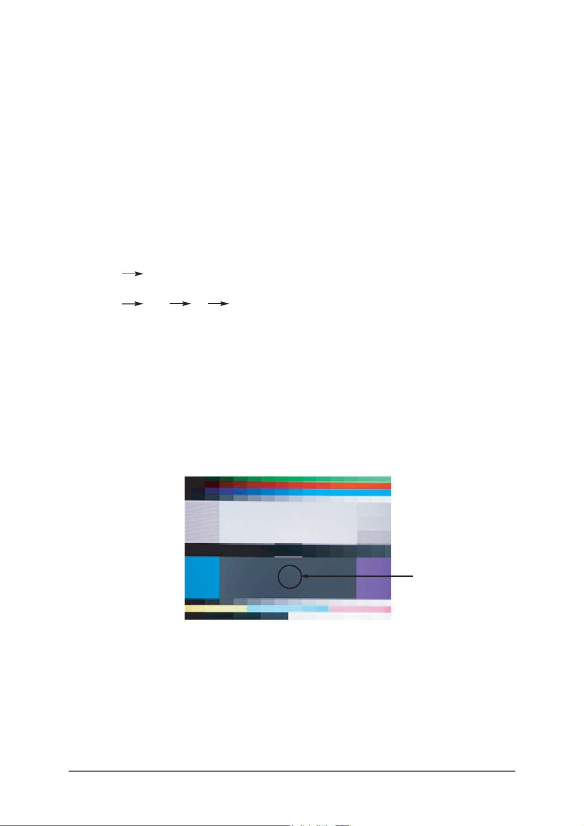
d) Adjust the high light. (Refer to table 1, 2 in adjustment position by mode)
- Adjust red gain ('x') and blue gain ('y') to the color coordinates.
* Do not adjust the green gain and sub-contrast (Y) data.
Picture 4-2 Flat W/B Pattern
Low light
Measurement point
3 Alignments and Adjustments
3-13
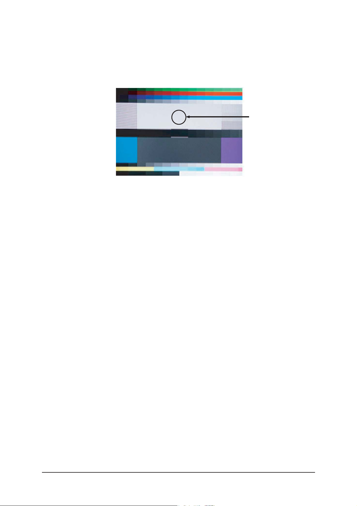
d) Adjust the high light. (Refer to table 1, 2 in adjustment position by mode)
- Adjust red gain ('x') and blue gain ('y') to the color coordinates.
* Do not adjust the green gain and sub-contrast (Y) data.
Picture 4-3 Flat W/B Pattern
High light
Measurement point
3 Alignments and Adjustments
3-14
3-5 Software Upgrade
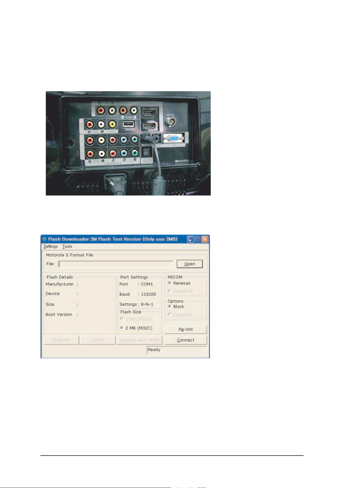
3-5-1 How to Update Flash ROM
1. Install the Flash Downloader
ConnectSet(Service Jack)and Jig Cable to execute Program Update.
2. Flash Downloader program update
-Before Turning on the set,Click "connect"which is under of OSD Screen!
-Turn on the Set.
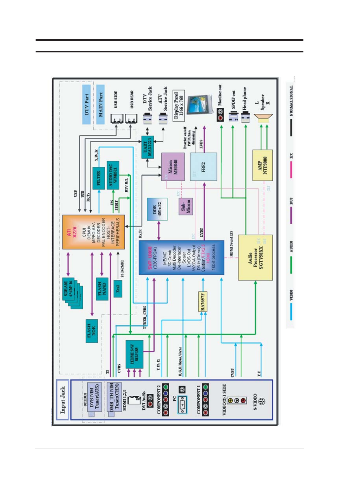
7 Block Diagrams
7-1
7 Block Diagram
- This Document can not be used without Samsung’s authorization

7 Block Diagrams
7-2
Memo
13 Circuit Descriptions
13-1
13 Circuit Descriptions
13-1 Main Signal Description
13-2 DTV Signal Description
13 Circuit Descriptions
13-2
13 Circuit Descriptions
13-3
13-3 RF/DTV Tuner (DNOS403MH261B(S)) SPEC.
1. Description
1-1 Receiving System : Designed to cover all bands in VHF and UHF including digital terrestrial(DVB-T)
and hyper channels for CCIR system.
1-2 It built in COFDM-Demod IC & Analog Demod IC (PAL B/G, I, D/K, SECAM L/L')
1-3 Receiving Channel : 47MHz ~ 862MHz
1-4 Intermediate Frequency : Digital(center) 36.167 MHz, Analog(picture) 38.9MHz
1-5 Input Impedance : 75§Ù, Unbalanced.
1-6 Terminals name and function
2. Mechanical Characteristics
2-1 Dimensions : refer Fig1
2-2 Weight : 60g
2-3 RF input : DIN jack(female)
2-4 Holding Strength of Ant jack.
Initial Inserting Force : 5.0kg max.
Extracting Force After 5 Cycles : 0.7kg min.
2-5 Terminal Strength
The terminal shall not withdraw to the inside
when a force of 1.0Kgf(9.8N) is applied to the end.
Fig - 2
Pin No
1
2
3
4
5
6
7
8
9
10
11
12
13
14
Pin No
15
16
17
18
19
20
21
22
23
24
25
26
27
28
Connection
N.C
SYNC
VALID
MD7
MD6
MD5
MD4
MD4
MD2
MD1
MD0
MPEG CLK
SDA
SCL
Connection
LNA 9V
RF AGC
5V
AFT
30V
N.C (AS)
RESET
ERROR
VIDEO OUT
N.C
SIF OUT
3.3V
GND
N.C
Remark
Only Analog part
Initial power-up,
Reset need Low status ¡Ã50mS
Remark
MPEG data output7
MPEG data output6
MPEG data output5
MPEG data output4
MPEG data output3
MPEG data output2
MPEG data output1
MPEG data output0

13 Circuit Descriptions
13-4
3. General Characteristics
3-1 Temperature Range
Storage Temperature : -20℃ ~ 45℃
Operation Temperature : 10℃ ~ 40℃
3-2 Test conditions : All data hold under following conditions
T(amb.) : +25±2℃ / Humidity : 45 ~ 65 % RH
Supply voltage(5V) : +5V ± 2%
Supply voltage(9V) : +9V ± 2%
Tuning voltage (BT) : +30V ± 2%
Supply voltage(3.3V) : +3.3V ± 2%
3-3 Current Consumption
Supply Voltage (5V) : Typ 210mA, Max 240mA
Supply Voltage (9V) : Typ 40mA, Max 70mA
Tuning Voltage(30V) : Max 2mA
Supply Voltage(3.3V) : Max 240mA Max 260mA
4. Electrical Characteristics ( RF block & Digital Demodulation )
4-1 Input Frequency Range
Analog VHF-Low Band : 48.25MHz ~ 168.25MHz
VHF-High Band : 175.25MHz ~ 463.25MHz
UHF Band : 471.25MHz ~ 855.25MHz
DVB-T VHF-High Band : 174(177.5)MHz ~ 230(226.5)MHz
UHF Band : 470(474)MHz ~ 862(858)MHz
4-2 Input Signal Level : -80dBm ~ -10dBm (AveragePower, 64QAM, 2/3CR)
4-3 Voltage Gain
1st IF : 40dB typ. 38dBmin.
4-4 Noise Figure
1st IF : 4.5dB typ. 6.5dB max. (at max. gain)
4-5 OFDM-Demod IC : MT5131 (produced by MediaTek)
4-6 Input Impedance : 75Ω
4-7 RF Input/Output Return Loss : -8dB typ. -6dB min.
4-8 IF Frequency
1) Digital center frequency : 36.125MHz
2) Analog (PAL B/G, I, D/K, SECAM L/L')
Picture intermediate frequency :
38.9MHz(PAL B/G & SECAM L), 33.9MHz(SECAM L')
Sound intermediate frequency :
33.4MHz(B/G), 32.9MHz(I), 32.4MHz(D/K,SECAM L), 40.4MHz(SECAM L')
4-9 Spurious Signals at Input Terminal
Local Oscillator Leakage : 46dBuV max.
4-10 Reference Frequency
The X-tal for the RF block's PLL : 4MHz

13 Circuit Descriptions
13-5
4-11 Phase Noise (step frequency 166.67kHz for digital)
@ 1kHz : -84dBc/Hz typ. -75dBc/Hz max.
@ 10kHz : -90dBc/Hz typ. -80dBc/Hz max.
4-12 Control Data Bus : I
2
C
4-13 Control Data Format : refer 5 section
4-14 Image PAL Interference Protection Ratio
: -49dB typ. -46dB min (at 2K, 8K mode) Note1.
4-15 Adjacent PAL Interference Protection Ratio. (N ±1 channel)
: -38dB typ. -35dB min (at 2K, 8K mode) Note1.
4-16 Adjacent DVB-T Interference Protection Ratio. (N ¡¾1 channel)
: -33dB typ. -30dB min (at 2K, 8K mode) Note1.
4-17 Co-Channel PAL Interference Ratio.
: +1dB typ. +4dB min (at 2K, 8K mode) Note1.
◆ Note1 :
Desire input signal condition
a : Modulation - 64QAM
b : Guard Interval - 1/32
c : Puncture Rate - 2/3
Undesired input signal condition :
PAL : Video 75% color bars
FM sound : 1kHz tone (P/S : 13dB, ± 50kHz deviation, freq. P/S : 6.0MHz)
※ Adjacent & Image channel PAL interference test procedure
a. Turn DVB-T source off ; adjust PAL PSP level to -25dBm
b. Turn PAL off ; turn DVB-T on
c. Adjust DVB-T to -25dBm
d. Turn PAL on and increase step PAL level to see the pixelation on the screen
e. Note protection ratio as the difference value between DVB-Tand PAL's level
※ Co-Channel PAL interference test procedure
a. Turn PAL source off ; adjust DVB-T level to -50dBm
b. Turn DVB-T off ; turn PAL on
c. Adjust PAL to -50dBm
d. Turn DVB-T on and increase step attenuator in PAL channel until QEF.
4-18 Input Carrier to Noise (Additive White Gaussian Noise, QEF. Condition)
: 17.4dB typ. 18.4dB max. (64QAM, 2K,8K Mode, Code rate:2/3, input level:-50dBm)
: 22.5dB typ. 23.5dB max. (64QAM, 2K,8K Mode, Code rate:7/8, input level:-50dBm)
4-19 Sensitivity (QEF. Condition)
: -80dBm typ. -78.5dBm max.(64QAM, 2K,8K Mode, Code rate:2/3,Guard Interval 1/32)
: -76dBm typ. -74.7dBm max.(64QAM, 2K,8K Mode, Code rate:7/8,Guard Interval 1/32)
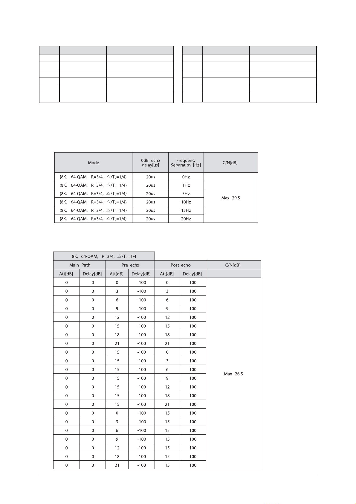
4-20 Multipath channel Interference (64QAM, 2K, 2/3code rate, 1/32G.I)
4-21 C(N+1) Performance in Single Frequency Networks outside the guard interval
- NorDig Unified Test Specification, ver 1.0 (Task 3.28)
13 Circuit Descriptions
13-6
Pin No
1
2
3
4
5
6
Delay(us)
0
0.05
0.4
1.45
2.3
2.8
Relative Attenuation(dB)
2.8
0
3.8
0.1
2.6
1.3
Pin No
1
2
3
4
5
6
Delay(us)
0
5
14
35
54
75
Relative Attenuation(dB)
0
9
22
25
27
28
13 Circuit Descriptions
13-7
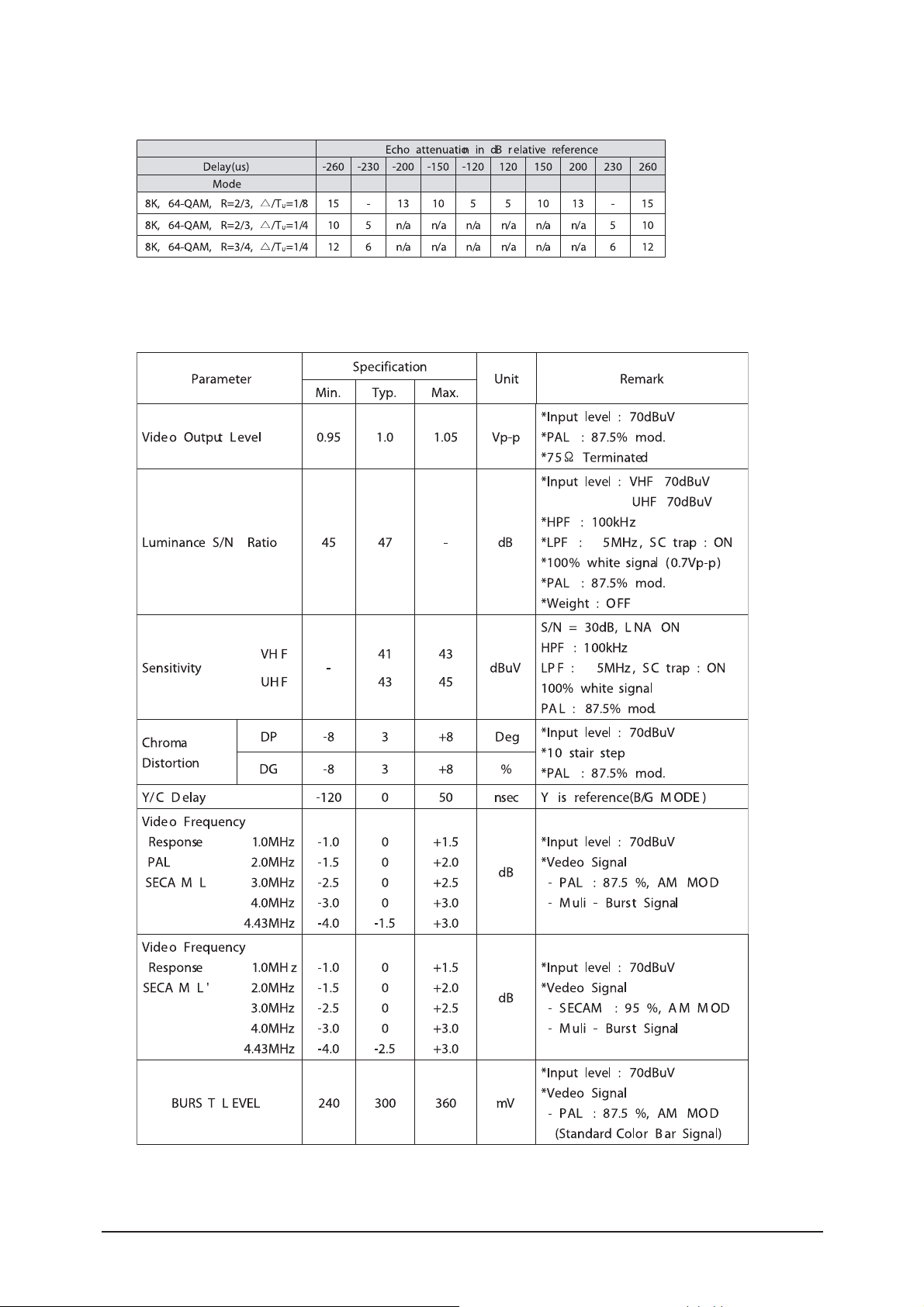
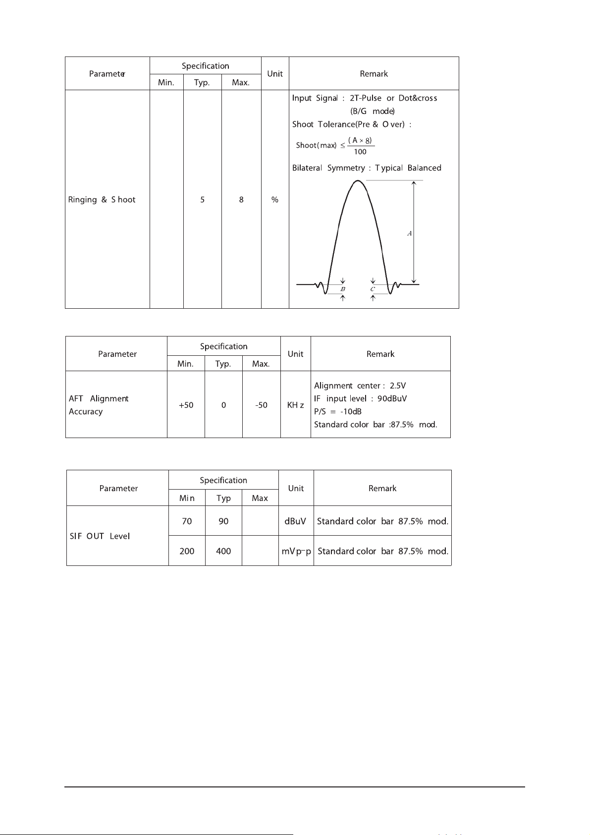
5. Electrical Characteristics ( Analog Demodulation )
5-1 PIF characteristics
13 Circuit Descriptions
13-8

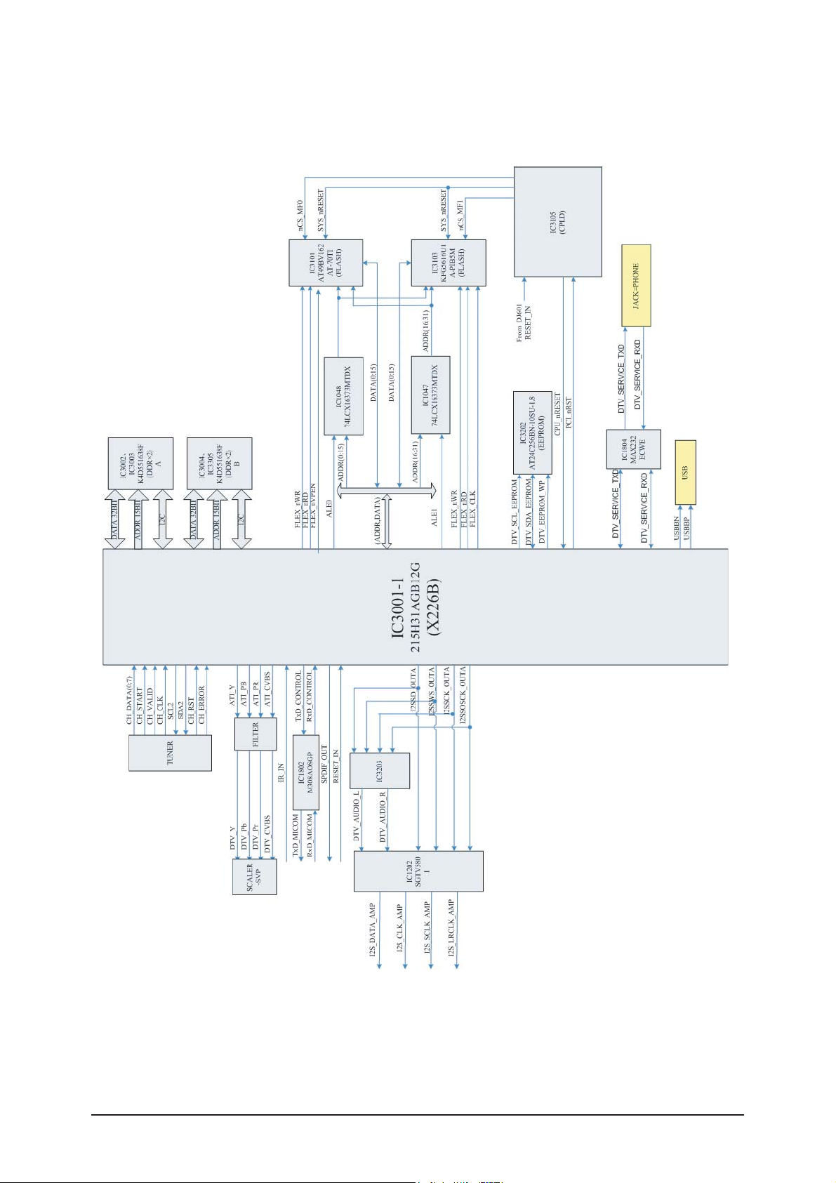
13 Circuit Descriptions
13-9
In almost all cases, the X226B is backward compatible in software and functionality with the X226A. In addition,
the X226B has the following significant feature enhancements over X226A:
Support for Simultaneous DVI (YCbCr601/YCbCr709/RGB) Out and DAC (YPbPr) Output on the Primary Display
with Constraint Image
- Support embedded CGMS-A (EIA/CEA-805, EIA-J-1204-2) information in the primary DAC HD YPbPr Output.
- Support 50Hz capture and display (but no frame rate convention from 50Hz to 60Hz, or vice versa), complaint with the
EIA/CEA-861-B standard for DAC Out and DVI Out, and the ANSI/SMPTE 295M-1997 standard for primary display
DAC Out only
- Support 12-bit or 15-bit DDR DVI Output up to 80MHz pixel clock with separate HSYNC, VSYNC, DE polarity control,
dither 10 bit to 8 bit for 12-bit DDR DVI Output, and flexible On-Screen Display (OSD) indicators.
- Support 8-bit ITU-656 Out HREF and VREF (DVSHREFC and DVSVREFC) on DVSYDATC(8) and DVSYDATC(9).
- Support Video / Video Alpha Blending using Global Alpha on PIP Windows at Video Scalar Output on Primary Display path.
- Support non-linear horizontal anamorphic scaling on secondary and third video scalars (besides primary video scalar).
Support programmable 10-bit lookup table for gamma correction on the primary display
Support "Serrated Edge Removal Algorithm" (SERATM) that performs motion adaptive jagged edge correction by removing
objectionable artifacts on moving diagonals of Standard Definition (SD) interlaced content
Support 24-bit SDR and 12-bit DDR PC Graphics RGB Input for DVI IN up to 108MHz pixel clock.
Wavegen to improve PLL pulling/stepping for HDTV mode - Use the fourth primary DAC (DAC3) to digitally synthesize a
pullable clock, route through external filters and input to PLL (through new LPBK_PCLK pin or IDE_DMARQ pin).
Bi-directional I/O 2nd IR Port for HDMI CEC signaling.
Additional Pin Multiplexing:
- DVI Input 12-bit DDR or 24-bit SDR input DVICLK from GPIOB(7) instead of GPIOA(13), and DVIHSYNC from GPIOB(6)
instead of GPIOB(7).
- Smart Card B SMVCCB multiplex through GPIOA(13) instead of GPIOB(6) to avoid conflict with DVIHSYNC above,
and swap SMDETECTB from GPIOB(18) to GPIOB(19), and swap SMDATAB from GPIOB(19) to GPIOB(18).
- DVI Input 24-bit SDR upper 12 bits data multiplex through IDE pins.
- DVI Output 12-bit or 15-bit DDR multiplex through one bit Graphics Alpha on FlexBus, Smart Card A and Shopping,
and 1st IR pins to avoid conflict with DVI Input on GPIOB bus, and avoid conflict with FlexBus FAD[15:8], FCEb(1) and
FALE(1) for NOR flash and POD host. For 12-bit DVI Output, optionally, NRSSCLKA can be used as a GPIO pin
(e.g. HDMI Output CEC function implement in GPIO instead of new IRBIDB pin) instead of being used as DVI Output Monitor
Sense (DVOMSEN).
- Either graphics alpha bit 2 to 0, or DVI Out DDC I2C multiplex through VCXO & PWM ports.
- Added GPIO capability on FCEb(1) pin (e.g. HDMI Input CEC function implemented through GPIO instead of through the
new IRBIDB pin).
- 3rd Serial Port/UART Port C multiplex through new RDC/TDC pins to avoid conflict with DVI Input on GPIOB(3:2).
- FlexBus Interrupt FINTR(6:4) multiplex through GPIOA(4:3,12) pins to avoid conflict with DVI Out on Smart Card Shopping pins.
- FRDYb multiplex through FCEb(1) pin to avoid conflict with VCXO_INB pin or DVOVSYNC on FRDYb pin.
- Display loopback PLL clock LPBK_PCLK input on either new LPBK_PCLK pin or IDE_DMARQ pin from DAC3 output
through external filters.
- 2nd IR multiplex on new RDC/TDC pin to avoid conflict with DVI Input on GPIOB(3:2).
- Bi-directional I/O 2nd IR port on new IRBIDB pin.
13-4 DTV MAIN ChipSet
13-5-1 ATIX226B SPEC.
 Loading...