

Page 1
LCD-TV
Chassis : N65E
Model : LE32B53*P7N
Manual
SERVICE
TFT-LCD TV contents
1. Precautions
2. Product specications
3. Disassembly and
4. Troubleshootin
5. Exploded View & Part Lis
6. Wiring Diagra
Reassembly
g
t
m
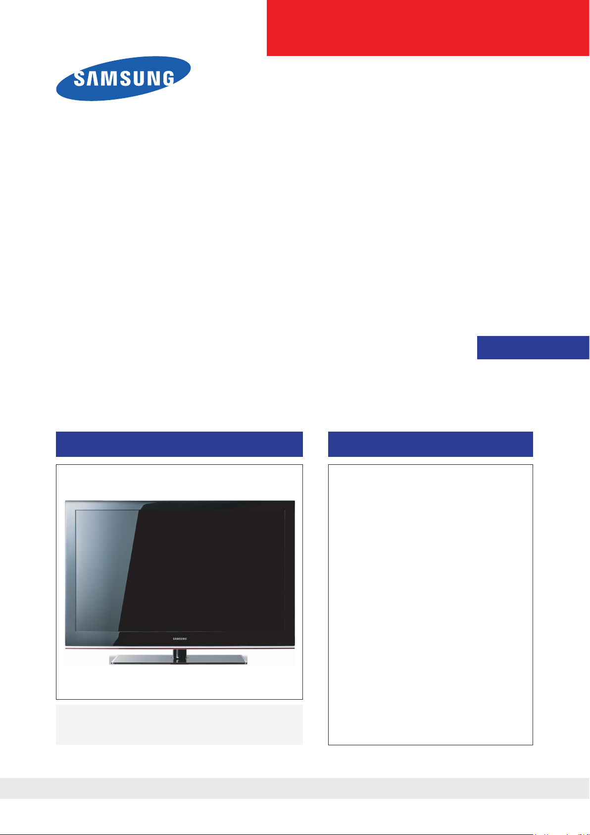
LE32B53*P7N
Refer to the service manual in the GSPN (see the rear cover) for the more information.
Page 2

Contents
1. Precautions .............................................................................................................. 1-1
1-1. Safety Precautions ......................................................................................................... 1-1
1-2. Servicing Precautions .....................................................................................................1-2
1-3. Electrostatically Sensitive Devices (ESD) Precautions .................................................. 1-2
1-4. Installation Precautions .................................................................................................. 1-3
2. Product specications ............................................................................................ 2-1
2-1. Feature & Specications ................................................................................................. 2-1
2-2. New Features explanation .............................................................................................. 2-5
2-3. Specication Comparison to Old Models ........................................................................ 2-6
2-4. Accessories .................................................................................................................... 2-7
3. Disassembly and Reassembly ............................................................................... 3-1
3-1. Disassembly and Reassembly ....................................................................................... 3-1
4. Troubleshooting ...................................................................................................... 4-1
4-1. Troubleshooting .............................................................................................................. 4-1
4-2. Alignments and Adjustments ........................................................................................ 4-25
4-3. Factory Mode Adjustments ........................................................................................... 4-26
4-4. White Balance - Calibration .......................................................................................... 4-37
4-5. White Ratio (Balance) Adjustment ................................................................................ 4-37
4-6. Servicing Information .................................................................................................... 4-38
4-7. S/W UPDATE MANUAL (use ISP TOOL & JIG) ........................................................... 4-39
4-8. Mechanical diagram ..................................................................................................... 4-42
5. Exploded View & Part List ...................................................................................... 5-1
5-1. LE32B53*P7N Exploded View ........................................................................................ 5-1
5-2. LE32B53*P7N Parts List ................................................................................................ 5-3
6. Wiring Diagram ........................................................................................................ 6-1
6-1. Wiring Diagram 32” ......................................................................................................... 6-1
6-2. Connector Functions ...................................................................................................... 6-5
6-3. Cables ............................................................................................................................ 6-5
Page 3

GSPN (Global Service Partner Network)
Area Web Site
North America
Latin America
CIS http://cis.samsungportal.com
Europe http://europe.samsungportal.com
China http://china.samsungportal.com
Asia http://asia.samsungportal.com
Mideast & Africa
This Service Manual is a property of Samsung Electronics Co.,Ltd.
Any unauthorized use of Manual can be punished under applicable
International and/or domestic law.
http://service.samsungportal.com
http://latin.samsungportal.com
http://mea.samsungportal.com
© 2009 Samsung Electronics Co.,Ltd.
All rights reserved.
Printed in Korea
P/N: BN82-00658A-00
Page 4
1. Precautions
1. Precautions
1-1. Safety Precautions
Follow these safety, servicing and ESD precautions to prevent damage and to protect against potential hazards such as
electrical shock.
1-1-1. Warnings
1.
For continued safety, do not attempt to modify the circuit board.
2.
Disconnect the AC power and DC power jack before servicing.
1-1-2. Servicing the LCD TV
1.
When servicing the LCD TV, Disconnect the AC line cord from the AC outlet.
2.
It is essential that service technicians have an accurate voltage meter available at all times.
Check the calibration of this meter periodically.
1-1-3. Fire and Shock Hazard
Before returning the LCD TV to the user, perform the following safety checks:
1.
Inspect each lead dress to make certain that the leads are not pinched or that hardware is not lodged between the
chassis and other metal parts in the LCD TV.
2.
Inspect all protective devices such as nonmetallic control knobs, insulating materials, cabinet backs, adjustment and
compartment covers or shields, isolation resistorcapacitor networks, mechanical insulators, etc.
3.
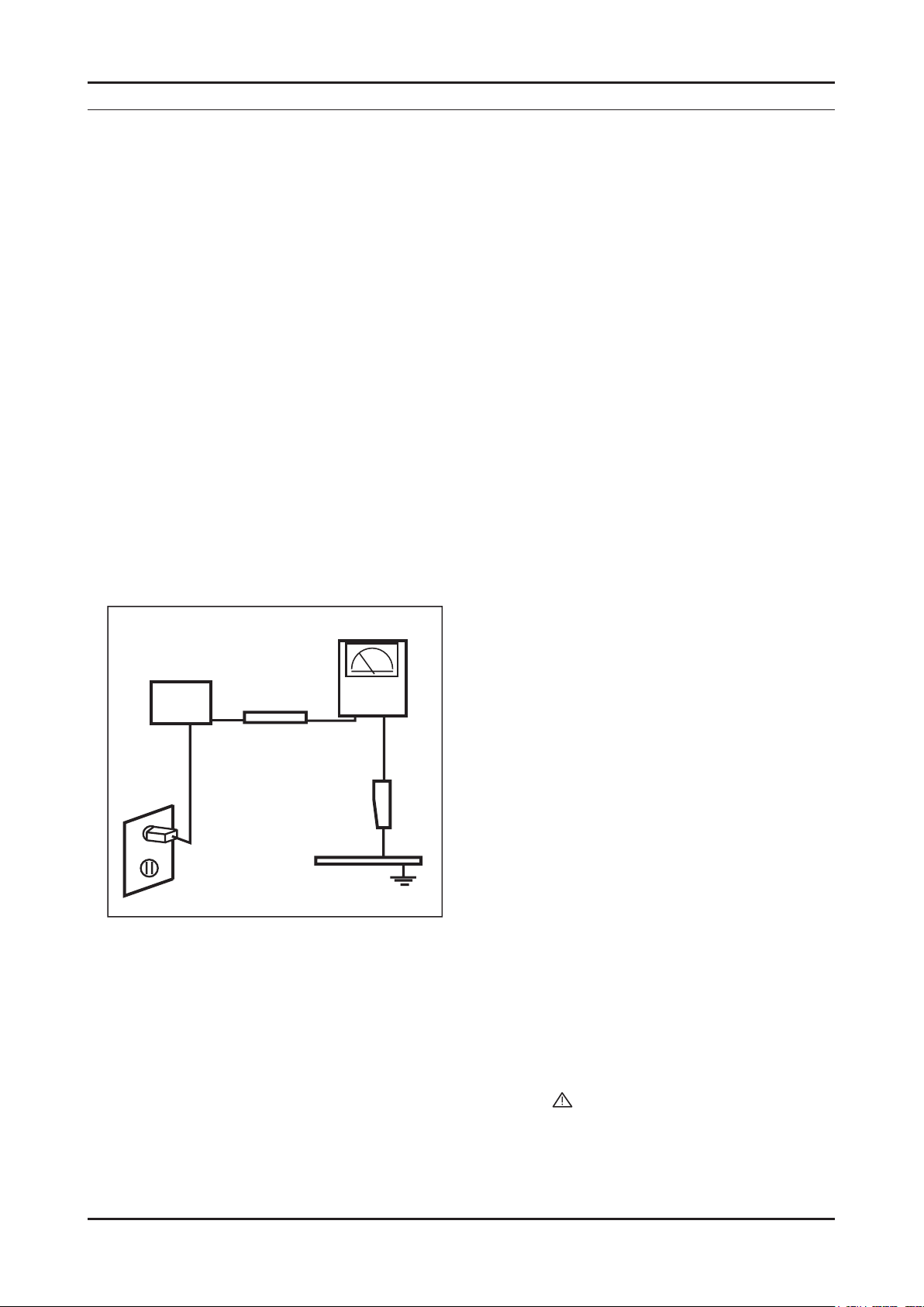
Leakage Current Hot Check (Figure 1-1):
WARNING : Do not use an isolation transformer during this test.
Use a leakage current tester or a metering system that complies with American National Standards Institute (ANSI
C101.1, Leakage Current for Appliances), and Underwriters Laboratories (UL Publication UL1410, 59.7).
(READING SHOULD)
NOT BE ABOVE 0.5mA
DEVICE
UNDER
TEST
TEST ALL
EXPOSED METAL
SURFACES
2-WIRE CORD
*ALSO TEST WITH
PLUG REVERSED
(USING AC ADAPTER
PLUG AS REQUIRED)
4.
With the unit completely reassembled, plug the AC line cord directly into a 120V AC outlet. With the unit’s AC switch
LEAKAGE
CURRENT
TESTER
EARTH
GROUND
Figure 1-1. Leakage Current Test Circuit
rst in the ON position and then OFF, measure the current between a known earth ground (metal water pipe, conduit,
etc.) and all exposed metal parts, including: metal cabinets, screwheads and control shafts.
The current measured should not exceed 0.5 milliamp.
Reverse the power-plug prongs in the AC outlet and repeat the test.
1-1-4. Product Safety Notices
Some electrical and mechanical parts have special safetyrelated characteristics which are often not evident from visual
inspection. The protection they give may not be obtained by replacing them with components rated for higher voltage,
wattage, etc. Parts that have special safety characteristics are identied by on schematics and parts lists. A substitute
replacement that does not have the same safety characteristics as the recommended replacement part might create
shock, re and/or other hazards. Product safety is under review continuously and new instructions are issued whenever
appropriate.
1-1
Page 5

1-2
1. Precautions
1-2. Servicing Precautions
WARNING: An electrolytic capacitor installed with the wrong polarity might explode.
Caution: Before servicing units covered by this service manual, read and follow the Safety Precautions section of
this manual.
Note:
1-2-1 General Servicing Precautions
1.
Always unplug the unit’s AC power cord from the AC power source and disconnect the DC Power Jack before
attempting to:
(a) remove or reinstall any component or assembly, (b) disconnect PCB plugs or connectors, (c) connect a test
component in parallel with an electrolytic capacitor.
2.
Some components are raised above the printed circuit board for safety. An insulation tube or tape is sometimes
used. The internal wiring is sometimes clamped to prevent contact with thermally hot components. Reinstall all such
elements to their original position.
3.
After servicing, always check that the screws, components and wiring have been correctly reinstalled. Make sure that
the area around the serviced part has not been damaged.
4.
Check the insulation between the blades of the AC plug and accessible conductive parts (examples: metal panels,
input terminals and earphone jacks).
5.
Insulation Checking Procedure: Disconnect the power cord from the AC source and turn the power switch ON.
Connect an insulation resistance meter (500 V) to theblades of the AC plug.
The insulation resistance between each blade of the AC plug and accessible conductive parts (see above) should be
greater than 1 megohm.
6.
Always connect a test instrument’s ground lead to the instrument chassis ground before connecting the positive lead;
always remove the instrument’s ground lead last.
If unforeseen circumstances create conict between the following servicing precautions and any of the
safety precautions, always follow the safety precautions.
1-3. Electrostatically Sensitive Devices (ESD) Precautions
Some semiconductor (solid state) devices can be easily damaged by static electricity. Such components are commonly
called Electrostatically Sensitive Devices (ESD). Examples of typical ESD are integrated circuits and some eld-effect
transistors. The following techniques will reduce the incidence of component damage caused by static electricity.
1.
Immediately before handling any semiconductor components or assemblies, drain the electrostatic charge from your
body by touching a known earth ground. Alternatively, wear a discharging wrist-strap device. To avoid a shock hazard,
be sure to remove the wrist strap before applying power to the LCD TV.
2.
After removing an ESD-equipped assembly, place it on a conductive surface such as aluminum foil to prevent
accumulation of an electrostatic charge.
3.
Do not use freon-propelled chemicals. These can generate electrical charges sufcient to damage ESDs.
4.
Use only a grounded-tip soldering iron to solder or desolder ESDs.
5.
Use only an anti-static solder removal device. Some solder removal devices not classied as “anti-static” can generate
electrical charges sufcient to damage ESDs.
6.
Do not remove a replacement ESD from its protective package until you are ready to install it. Most replacement ESDs
are packaged with leads that are electrically shorted together by conductive foam, aluminum foil or other conductive
materials.
7.
Immediately before removing the protective material from the leads of a replacement ESD, touch the protective
material to the chassis or circuit assembly into which the device will be installed.
Caution: Be sure no power is applied to the chassis or circuit and observe all other safety precautions.
8.
Minimize body motions when handling unpackaged replacement ESDs. Motions such as brushing clothes together,
or lifting your foot from a carpeted oor can generate enough static electricity to damage an ESD.
Page 6

1. Precautions
1-4. Installation Precautions
For safety reasons, more than a people are required for carrying the product.
1.
Keep the power cord away from any heat emitting devices, as a melted covering may cause re or electric shock.
2.
Do not place the product in areas with poor ventilation such as a bookshelf or closet. The increased internal
3.
temperature may cause re.
Bend the external antenna cable when connecting it to the product. This is a measure to protect it from being exposed
4.
to moisture. Otherwise, it may cause a re or electric shock.
Make sure to turn the power off and unplug the power cord from the outlet before repositioning the product. Also check
5.
the antenna cable or the external connectors if they are fully unplugged. Damage to the cord may cause re or electric
shock.
Keep the antenna far away from any high-voltage cables and install it rmly. Contact with the highvoltage cable or the
6.
antenna falling over may cause re or electric shock.
When installing the product, leave enough space (0.4m) between the product and the wall for ventilation purposes.
7.
A rise in temperature within the product may cause re.
1-3
Page 7

1. Precautions
Memo
1-4
Page 8
2. Product specications
2-1. Feature & Specications
Model LE32B53*P7N
Feature
DTV/ATV, 3-HDMI, 1-Component, 1-A/V, D-SUB, 1-SCART
�
Brightness : 500cd/m
�
High Contrast Ratio : 50,000:1
�
Response Time : 6.5ms
�
Item Description
LCD Panel DTV/ATV, 3-HDMI, 1-Component, 1-A/V, D-SUB, 1-SCART
Scanning Frequency Horizontal : 30 kHz ~ 80 kHz (Automatic)
Display Colors 16.7 million colors
Maximum resolution Horizontal : 1920 Pixels
2
Specications
Vertical : 47 Hz ~ 75 Hz (Automatic)
Vertical : 1080 pixels
2. Product specications
Input Signal Analog 0.7 Vp-p ± 5% positive at 75Ω , internally terminated
Input Sync Signal H/V Separate, TTL, P. or N.
Maximum Pixel Clock rate 310MHz
Active Display
Horizontal/Vertical
AC power voltage & Frequency AC 110V ~ 220V, 60 Hz
Power Consumption <130W (<1W, stand by )
Dimensions
Set (W x D x H)
Weight 12.9 kg
TV System Tunning Frequency Synthesize (Refer to detailed Frequency Table)
Environmental Considerations Operating Temperature : 50˚F ~ 104˚F (10˚C ~ 40˚C)
Audio Spec. - MAX Internal speaker Out : Right => 10W, Left => 10W
27.47 x 15.44 inches (697.68(H) x 392.26(V)mm)
801 x 87.7 x 158.1 mm_with stand
801 x 220.2 x 562.5 mm_without stand
System DVB-T/C, PAL, SECAM, NT4.43
Sound BG, DK, L/L’, NICAM, MPEG1, DD, DD+, HE-AAC
Operating Humidity : 10% ~ 80%, non-condensing
Storage temperature : -13˚F ~ 113˚F (-25˚C ~ 45˚C)
Storage Humidity : 5% ~ 95%, non-condensing
- BASS Control Range : -8 dB ~ + 8dB
- TREBLE Control Range : -8 dB ~ +8 dB
- Headphone Out : 10 mW MAX
- Output Frequency : RF : 80 Hz ~ 15 kHz
A/V : 80 Hz ~ 20 kHz
Note: TruSurround HD, Film Mode, Energy Saving, Anynet+
2-1
Page 9
2. Product specications
Channel UK France Germany Italy Spain Sweden Finland
VHF
[A] 56
[B] 64.5
[C] 84.5
[D] 177.5
[5] 178.75 [5] 177.5 [E] 186 [5] 177.5 [5] 177.5
[6] 186.75 [6] 184.5 [F] 194.5 [6] 184.5 [6] 184.5
[7] 194.75 [7] 191.5 [G] 203.5 [7] 191.5 [7] 191.5
[8] 202.75 [8] 198.5 [H] 212.5 [8] 198.5 [8] 198.5
[9] 210.75 [9] 205.5 [H1] 219.5 [9] 205.5 [9] 205.5
[10] 218.75
[10] 212.5 [H2] 226.5 [10] 212.5
[10] 212.5
[11] 219.5 [11] 219.5
[11] 219.5
[12] 226.5 [12] 226.5
[12] 226.5
UHF
21 474 474 474 474 474 474 474
22 482 482 482 482 482 482 482
23 490 490 490 490 490 490 490
24 498 498 498 498 498 498 498
25 506 506 506 506 506 506 506
26 514 514 514 514 514 514 514
27 522 522 522 522 522 522 522
28 530 530 530 530 530 530 530
29 538 538 538 538 538 538 538
30 546 546 546 546 546 546 546
31 554 554 554 554 554 554 554
32 562 562 562 562 562 562 562
33 570 570 570 570 570 570 570
34 578 578 578 578 578 578 578
35 586 586 586 586 586 586 586
36 594 594 594 594 594 594 594
37 602 602 602 602 602 602 602
38 610 610 610 610 610 610 610
39 618 618 618 618 618 618 618
40 626 626 626 626 626 626 626
41 634 634 634 634 634 634 634
42 642 642 642 642 642 642 642
43 650 650 650 650 650 650 650
44 658 658 658 658 658 658 658
45 666 666 666 666 666 666 666
46 674 674 674 674 674 674 674
47 682 682 682 682 682 682 682
48 690 690 690 690 690 690 690
49 698 698 698 698 698 698 698
50 706 706 706 706 706 706 706
51 714 714 714 714 714 714 714
52 722 722 722 722 722 722 722
53 730 730 730 730 730 730 730
54 738 738 738 738 738 738 738
55 746 746 746 746 746 746 746
56 754 754 754 754 754 754 754
57 762 762 762 762 762 762 762
58 770 770 770 770 770 770 770
59 778 778 778 778 778 778 778
60 786 786 786 786 786 786 786
61 794 794 794 794 794 794 794
62 802 802 802 802 802 802 802
63 810 810 810 810 810 810 810
64 818 818 818 818 818 818 818
65 826 826 826 826 826 826 826
66 834 834 834 834 834 834 834
67 842 842 842 842 842 842 842
68 850 850 850 850 850 850 850
69 858 858 858 858 858 858
Frequency (DTV)
2-2
Page 10
Australia Netherlands China Hongkong Taiwan
[0] 48.5 [1]52. 5
[1] 59.5
[2]60.5
[2] 66.5
[3]68.5
[3] 88.5
[4]80
[4] 97.5 [5] 174.5
[5]88
[5] 104.5 [6] 181.5
[6]171
[5A] 140.5 [7] 188.5
[7]179
[6] 177.5 [8] 195.5
[8]187
[7] 184.5 [9] 202.5
[9]195
[8] 191.5 [10] 209.5
[10]203
[9] 198.5 [11] 216.5
[11]211
[9A] 205.5 [12] 223.5
[12]219
[10] 212.5
[11] 219.5
[12] 226.5
474 [13]474 [21]474 [14]473
482 [14]482 [22]482 [15]479
490 [15]490 [23]490 [16]485
498 [16]498 [24]498 [17]491
506 [17]506 [25]506 [18]497
514 [18]514 [26]514 [19]503
520~526, 6MHz
522 [19]522 [27]522 [20]509
529.5 530 [20]530 [28]530 [21]515
536.5 538 [21]538 [29]538 [22]521
543.5 546 [22]546 [30]546 [23]527
550.5 554 [23]554 [31]554 [24]533
557.5 562 [24]562 [32]562 [25]539
564.5 570 [25]610 [33]570 [26]545
571.5 578 [26]618 [34]578 [27]551
578.5 586 [27]626 [35]586 [28]557
585.5 594 [28]634 [36]594 [29]563
592.5 602 [29]642 [37]602 [30]569
599.5 610 [30]650 [38]610 [31]575
606.5 618 [31]658 [39]618 [32]581
613.5 626 [32]666 [40]626 [33]587
620.5 634 [33]674 [41]634 [34]593
627.5 642 [34]682 [42]642 [35]599
634.5 650 [35]690 [43]650 [36]605
641.5 658 [36]698 [44]658 [37]611
648.5 666 [37]706 [45]666 [38]617
655.5 674 [38]714 [46]674 [39]623
662.5 682 [39]722 [47]682 [40]629
669.5 690 [40]730 [48]690 [41]635
676.5 698 [41]738 [49]698 [42]641
683.5 706 [42]746 [50]706 [43]647
690.5 714 [43]754 [51]714 [44]653
697.5 722 [44]762 [52]722 [45]659
704.5 730 [45]770 [53]730 [46]665
711.5 738 [46]778 [54]738 [47]671
718.5 746 [47]786 [55]746 [48]677
725.5 754 [48]794 [56]754 [49]683
732.5 762 [49]802 [57]762 [50]689
739.5 770 [50]810 [58]770 [51]695
746.5 778 [51]818 [59]778 [52]701
753.5 786 [52]826 [60]786 [53]707
760.5 794 [53]834 [61]794 [54]713
767.5 802 [54]842 [62]802 [55]719
774.5 810 [55]850 [63]810 [56]725
781.5 818 [56]858 [64]818 [57]731
788.5 826 [57]866 [65]826 [58]737
795.5 834 [58]874 [66]834 [59]743
802.5 842 [59]882 [67]842 [60]749
809.5 850 [60]890 [68]850 [61]755
816.5 858 [61]898 [69]858 [62]761
[62]906 [63]767
[63]914 [64]773
[65]779
[66]785
[67]791
[68]797
[69]803
2. Product specications
2-3
Page 11
2. Product specications
CH
NEWZEAL CHINA
(PAL D/K)
1 69-855.25 49.25
69-855.25
176.00 69-855.25 45.25 49.25
2 48.25 E2-48.25 59.25 184.00 FA-47.75 55.25 57.25
3 55.25 E3-55.25 77.25 192.00 FB-55.75 62.25 65.25
4 62.25 E4-62.25 85.25 200.00
FC1-60.50
175.25 77.25
5 175.25 X -69.25 93.25 208.00 FC-53.75 182.25 85.25
6 182.25 Y -76.25 175.25 216.00 B-116.75 189.25 168.25
7 189.25 Z -83.25 183.25 C-128.25 196.25 176.25
8 196.25 Z1-90.25 191.25 D-140.75 203.25 184.25
9 203.25 Z2-97.25 199.25 E-152.75 210.25 192.25
10 210.25 S1-105.25 207.25 F-164.75 217.25 200.25
11 217.25 S2-112.25 215.25 F1-176.00 224.25 208.25
12 224.25 S3-119.25 223.25 G -176.75 216.25
13 S4-126.25 F2-184.00 471.25
14 S5-133.25 H -188.75 479.25
15 S6-140.25 F3-192.00 487.25
16 S7-147.25 F4-200.00 495.25
17 S8-154.25 I -200.75 503.25
18 S9-161.25 F5-208.00 511.25
19 S10-168.25 J -212.75 519.25
20 E5-175.25 F6-216.00 527.25
21 471.25 E6-182.25 471.25 471.25 K -224.75 535.25
22 479.25 E7-189.25 479.25 479.25 L -236.75 543.25
23 487.25 E8-196.25 487.25 487.25 M -248.75 551.25
24 495.25 E9-203.25 495.25 495.25 N -260.75 559.25
25 503.25
E10-210.25
503.25 503.25 O -272.75 607.25
26 511.25
E11-217.25
511.25 511.25 P -284.75 615.25
27 519.25
E12-224.25
519.25 519.25 Q -296.75 623.25
28 527.25
S11-231.25
527.25 527.25 631.25
29 535.25
S12-238.25
535.25 535.25 639.25
30 543.25
S13-245.25
543.25 543.25 647.25
31 551.25
S14-252.25
551.25 551.25 655.25
32 559.25
S15-259.25
559.25 559.25 663.25
33 567.25
S16-266.25
567.25 567.25 671.25
34 575.25
S17-273.25
575.25 575.25 679.25
35 583.25
S18-280.25
583.25 583.25 687.25
36 591.25
S19-287.25
591.25 591.25 695.25
37 599.25
S20-294.25
599.25 599.25 703.25
38 607.25
S21-303.25
607.25 607.25 711.25
39 615.25
S22-311.25
615.25 615.25 719.25
40 623.25
S23-319.25
623.25 623.25 727.25
41 631.25
S24-327.25
631.25 631.25 735.25
42 639.25
S25-335.25
639.25 639.25 743.25
43 647.25
S26-343.25
647.25 647.25 751.25
44 655.25
S27-351.25
655.25 655.25 759.25
45 663.25
S28-359.25
663.25 663.25 767.25
46 671.25
S29-367.25
671.25 671.25 775.25
47 679.25
S30-375.25
679.25 679.25 783.25
48 687.25
S31-383.25
687.25 687.25 791.25
49 695.25
S32-391.25
695.25 695.25 799.25
50 703.25
S33-399.25
703.25 703.25 807.25
51 711.25
S34-407.25
711.25 711.25 815.25
52 719.25
S35-415.25
719.25 719.25 823.25
53 727.25
S36-423.25
727.25 727.25 831.25
54 735.25
S37-431.25
735.25 735.25 839.25
55 743.25
S38-439.25
743.25 743.25 847.25
56 751.25
S39-447.25
751.25 751.25 855.25
57 759.25
S40-455.25
759.25 759.25 863.25
58 767.25
S41-463.25
767.25 767.25 871.25
59 775.25 775.25 775.25 879.25
60 783.25 783.25 783.25 887.25
61 791.25 791.25 791.25 895.25
62 799.25 799.25 799.25 903.25
63 807.25 807.25 807.25 911.25
64 815.25 815.25 815.25 919.25
65 823.25 823.25 823.25 927.25
66 831.25 831.25 831.25 935.25
67 839.25 839.25 839.25 943.25
68 847.25 847.25 847.25 951.25
FRANCE
(SECAM-L)
CCIR
(PAL B/G)
OIRT
(SECAM D/K)
Frequency (ATV)
2-4
Page 12
2. Product specications
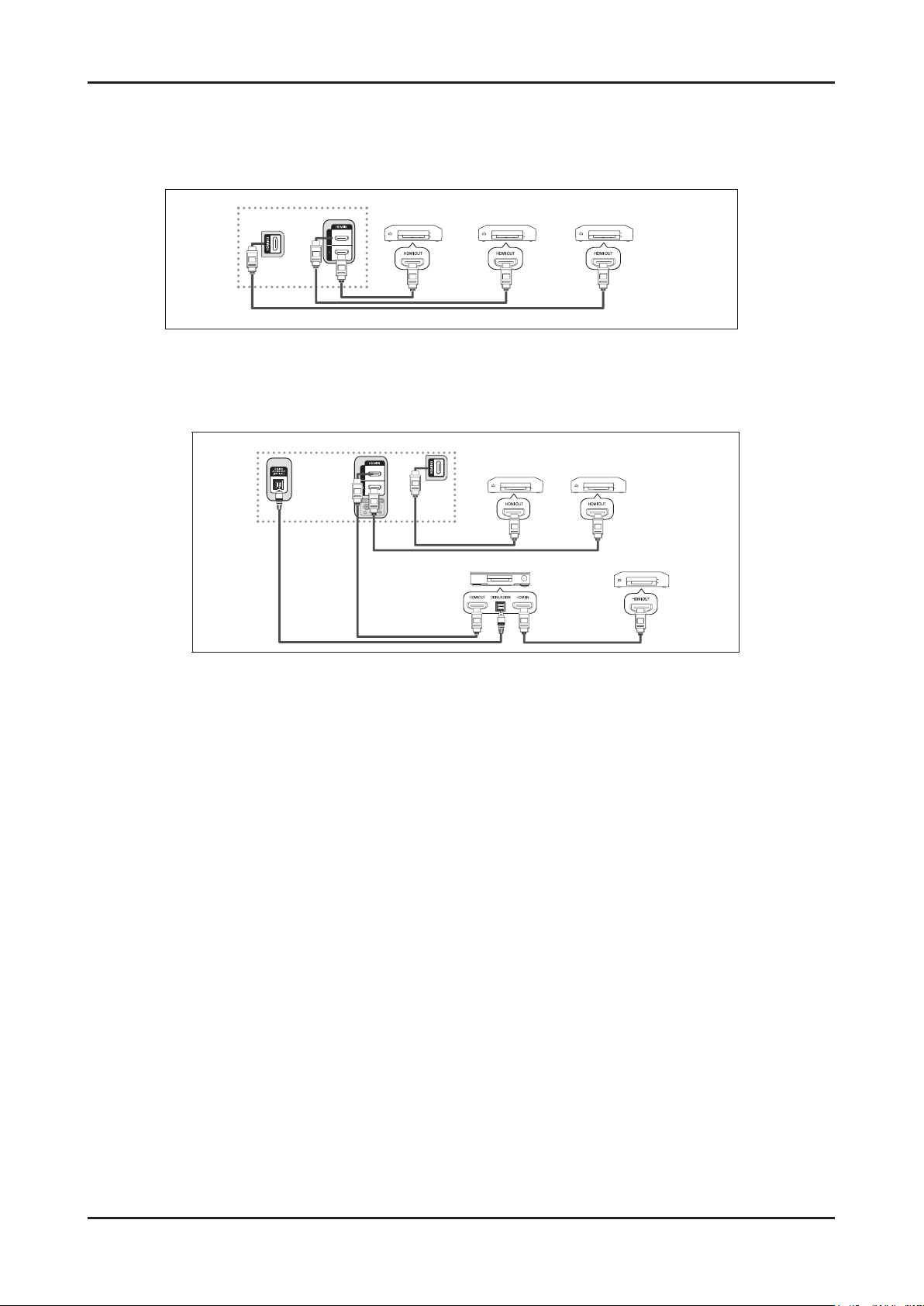
TV
Anynet+ Device 1
Anynet+ Device 2 Anynet+ Device 3
HDMI 1.3 Cable
HDMI 1.3 Cable
HDMI 1.3 Cable
TV
Anynet+ Device 1
Anynet+ Device 2
Anynet+ Device 3
HDMI 1.3 Cable
HDMI 1.3 Cable
HDMI 1.3 Cable
Optical Cable
Home Theater
HDMI 1.3 Cable
2-2. New Features explanation
Anynet+: Anynet+ is an AV network system that enables you to control all connected Samsung AV devices
�
with the TV’s remote.
To directly connect to TV
Connect the [HDMI 1], [HDMI 2] or [HDMI ] jack on the TV and the HDMI OUT jack of the corresponding
Anynet+ device using an HDMI cable.
To connect to Home Theater
Connect the [HDMI 1], [HDMI 2] or [HDMI ] jack on the TV and the HDMI OUT jack of the corresponding Anynet+
1.
device using an HDMI cable.
Connect the HDMI IN jack of the home theater and the HDMI OUT jack of the corresponding Anynet+
2.
device using the HDMI cable.
- Connect the Optical cable between [Digital Audio Out (Optical)] on your TV and Digital Audio Input on the
Home Theater.
- When following the connection above, the Optical jack only outputs 2 channel audio. You will only hear sound from
the Home Theater’s Front Left and Right speakers and the subwoofer. If you want to hear 5.1 channel audi
connect the DIGITAL AUDIO OUT (OPTICAL) jack on the DVD / Satellite Box (ie Anynet Device 1 or 2) directly
to the Ampli er or Home Theater, not the TV.
- Connect only one Home Theater.
- You can connect an Anynet+ device using the HDMI 1.3 cable. Some HDMI cables may not support Anynet+
functions.
- Anynet+ works when the AV device supporting Anynet+ is in the Standby or On status.
- Anynet+ supports up to 12 AV devices in total. Note that you can connect up to 3 devices of the same type.
2-5
Page 13
2. Product specications
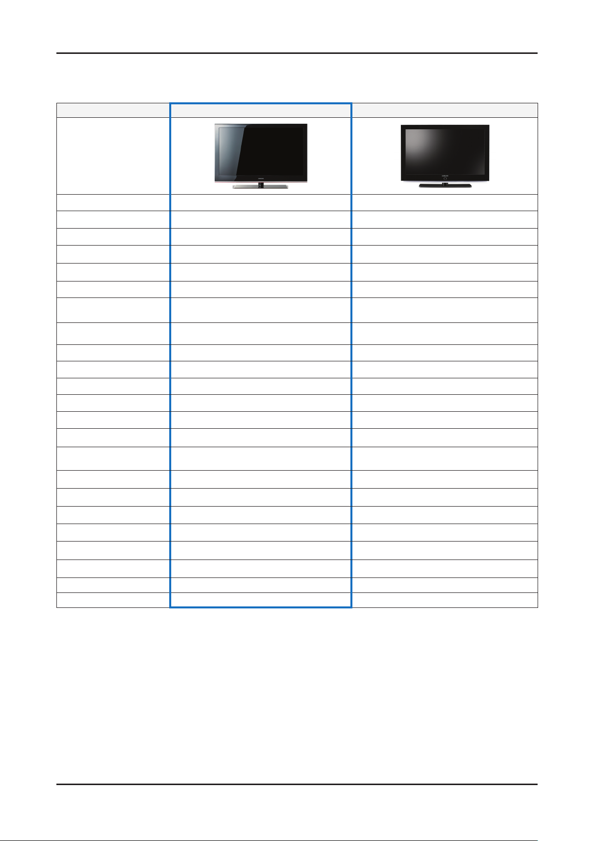
2-3. Specication Comparison to Old Models
O : application, X : non-application
※
Model B530(LE32B53*P7N) A530(LE32A53***)
Design
Display Type LCD TV LCD TV
Built-in Tuner O O
Resolution 1920 x 1080 1920 x 1080
LCD Panel TFT LCD Panel TFT LCD Panel
Screen Size 32” 32”
Picture ratio 16 : 9 16 : 9
Dimensions (W x H x D) 31.9 x 22.1 x 8.7 inchs_with stand 34.1 x 22.1 x 8.7 inchs_with stand
Weight 27.96 lbs_with stand 30.20 lbs_with stand
Brightness 500 cd
Contrast Ratio 50,000:1 50,000:1
Picture Enhacer DNIe (SEMS12) DNIe (FBE3)
Equalizer 5 Band 5 Band
Auto Volume Control O O
Surround Sound SRS TruSurround HD SRS TruSurround XT
Speaker Output 10W + 10W 10W + 10W
PIP X O
Double Window X O
TTX O O
Entertainment Mode X O
Game Mode O X
Energy Saving O O
Anynet+ O O
Antenna 1(Cable/Air) 1(Cable/Air)
2
500 cd
2
2-6
Page 14
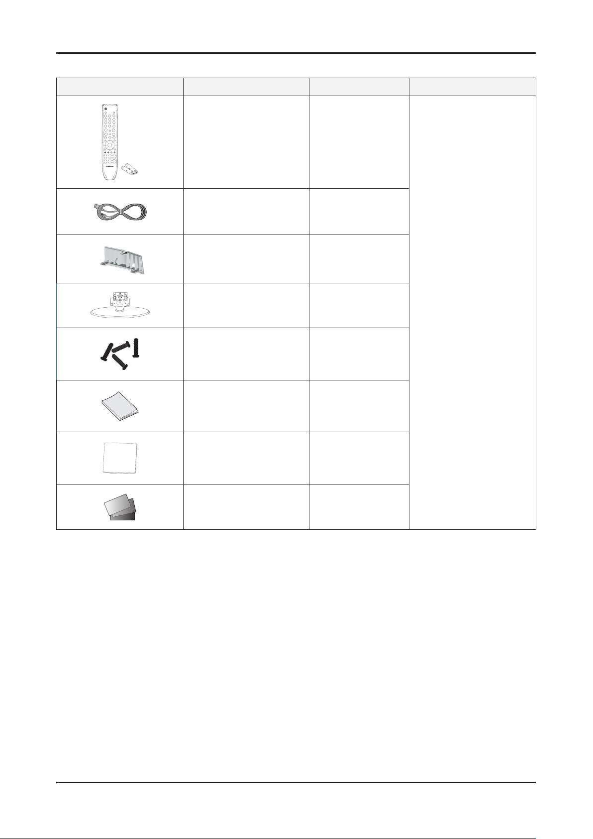
2-4. Accessories
Product Description Code. No Remark
2. Product specications
Remote Control & Batteries
(AAA x 2)
Power Cord 3903-000144
Cover-Bottom BN63-05356A
Stand BN96-09131A
Screw
(for the stand - M4, L6)
Owner’s Instructions BN68-02274A
BN59-00856A
6002-001294
Samsung Electronics
Service center
Cleaning Cloth BN-63-01798B
Warranty Card / Registration
Card / Safety Guide Manual
(Not available in all locations)
AA68-03242L
2-7
Page 15
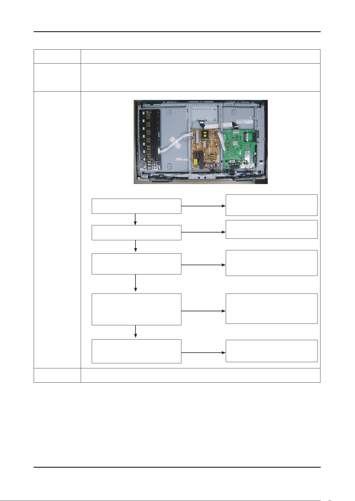
3. Disassembly and Reassembly
3. Disassembly and Reassembly
This section of the service manual describes the disassembly and reassembly procedures for the B530(LE32B53*P7N)
LCD TV.
WARNING: This LCD TV contains electrostatically sensitive devices. Use caution when handling these components.
3-1. Disassembly and Reassembly
Cautions: 1. Disconnect the LCD TV from the power source before disassembly.
2. Follow these directions carefully; never use metal instruments to pry apart the cabinet.
3. For Disassembly and Reassembly, (+) screw driver is used.
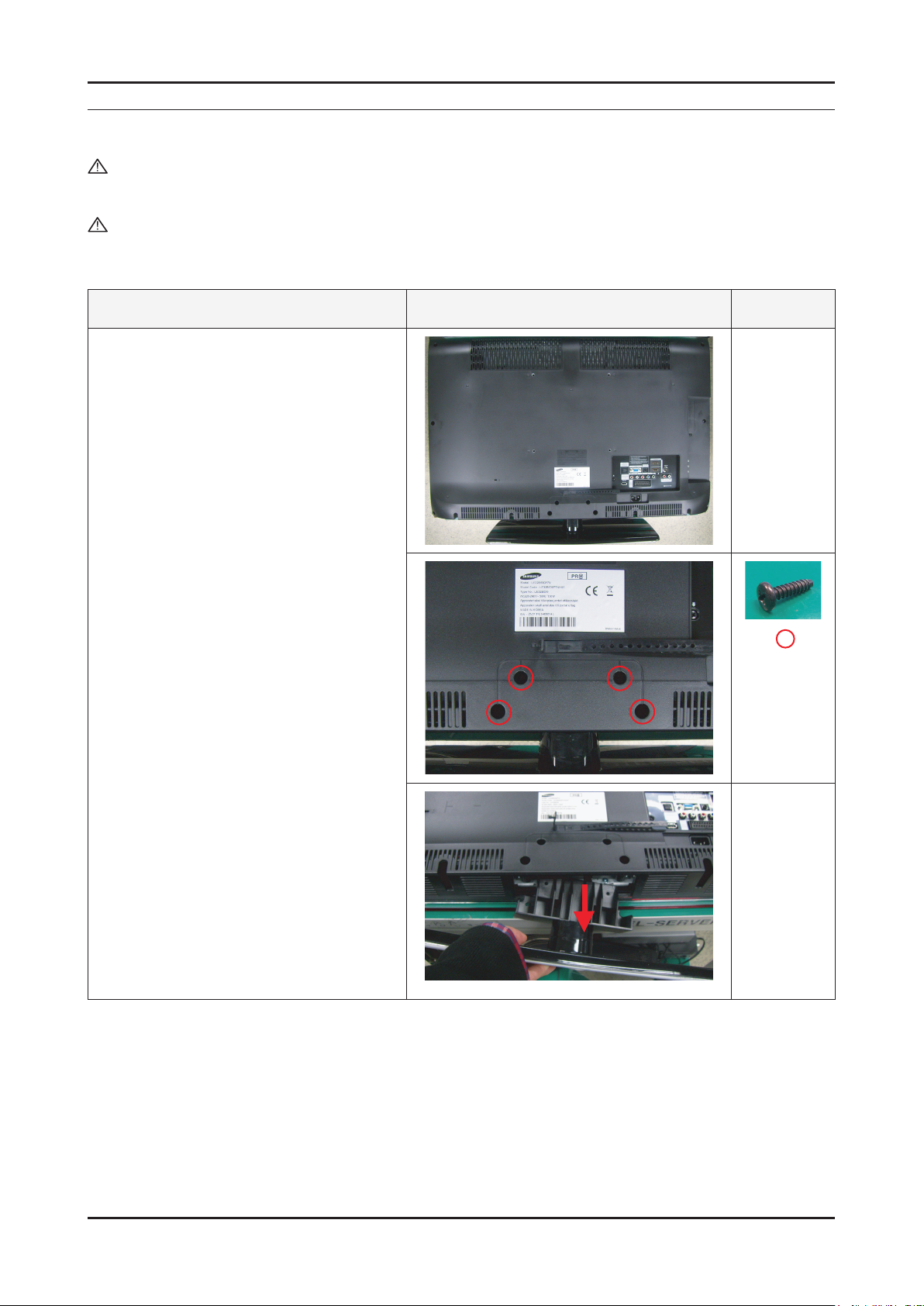
Description Picture Description Screws
1. Place the TV face down on cushioned table.
Remove 4 screws from the Stand.
Remove stand.
3-1
Page 16
3. Disassembly and Reassembly
Description Picture Description Screws
2. Remove the 14 screws of rear-cover.
3. Lift up the rear-cover.
4. Disconnect the cable.
5. Remove the left and right speaker.
3-2
Page 17
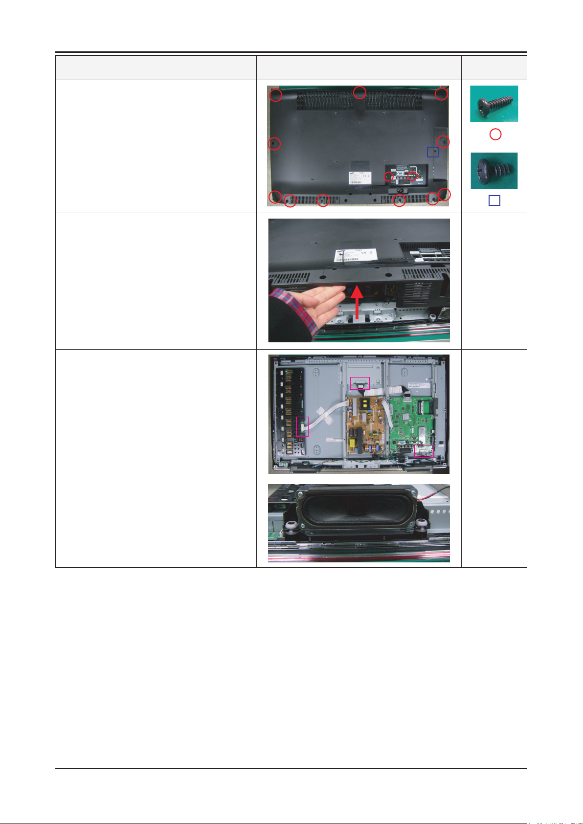
Description Picture Description Screws
TOP
BOTTOM
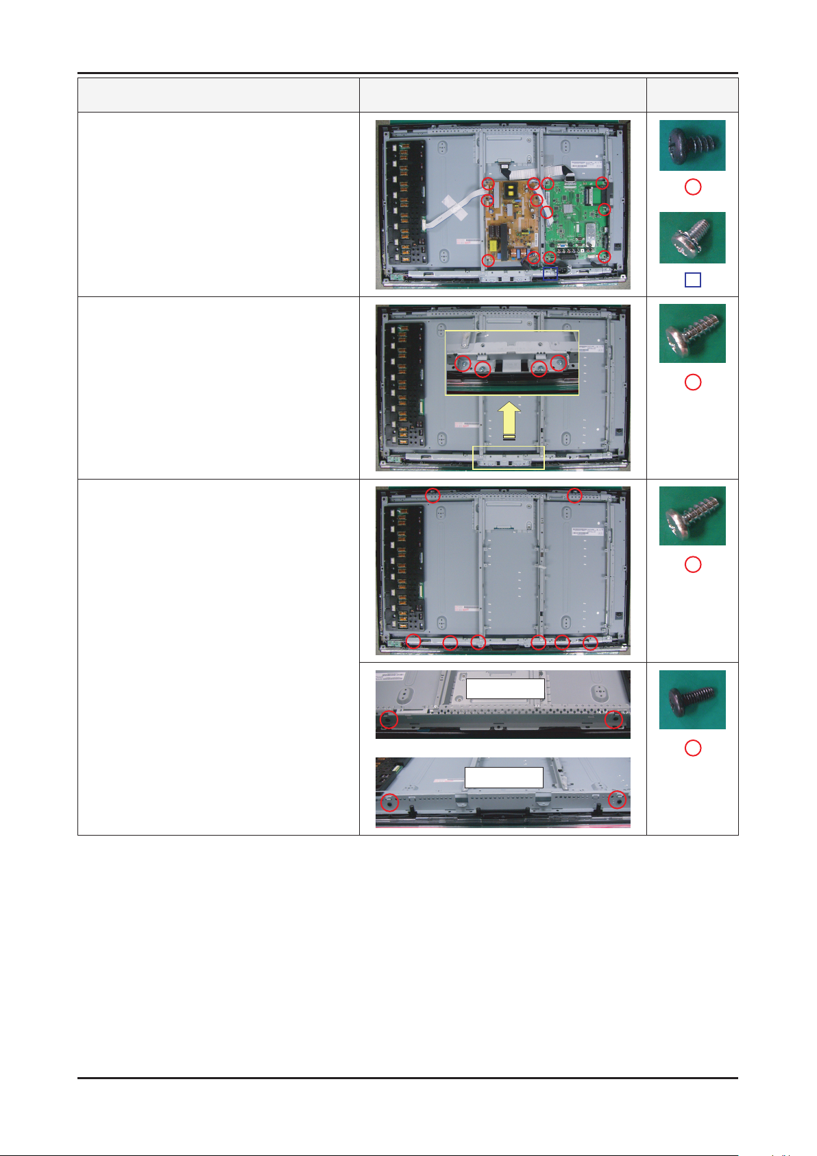
6. Remove the 6 screws of main board and
6 screws of IP board and 1 screw of inlet
socket.
7. Remove the 4 screws of bracket stand link.
3. Disassembly and Reassembly
8. Remove the 12 screws of bracket. Lift up the
bracket.
3-3
Page 18
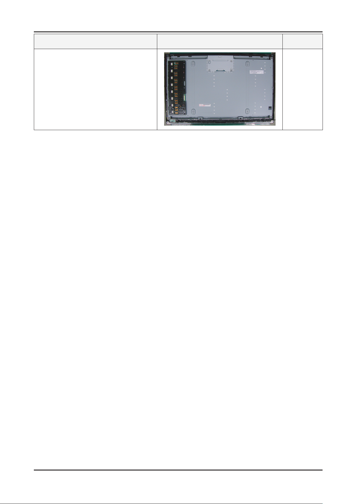
3. Disassembly and Reassembly
Description Picture Description Screws
9. Lift up the panel.
Reassembly procedures are in the reverse order of disassembly procedures.
※
3-4
Page 19

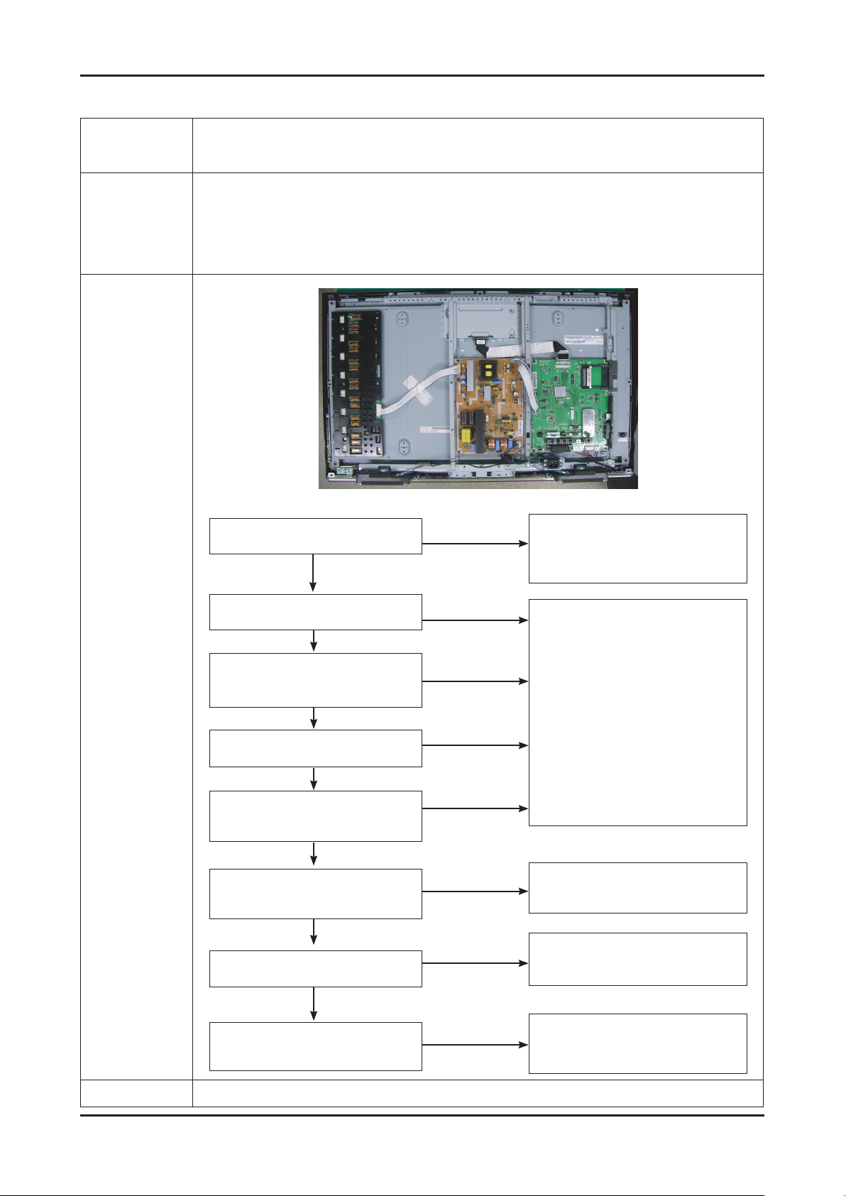
4. Troubleshooting
4-1. Troubleshooting
4-1-1. Previous check
Check the various cable connections rst.
1.
• Check to see if there is a burnt or damaged cable.
• Check to see if there is a disconnected or loose cable connection.
• Check to see if the cables are connected according to the connection diagram.
Check the power input to the Main Board.
2.
4. Troubleshooting
4-1
Page 20
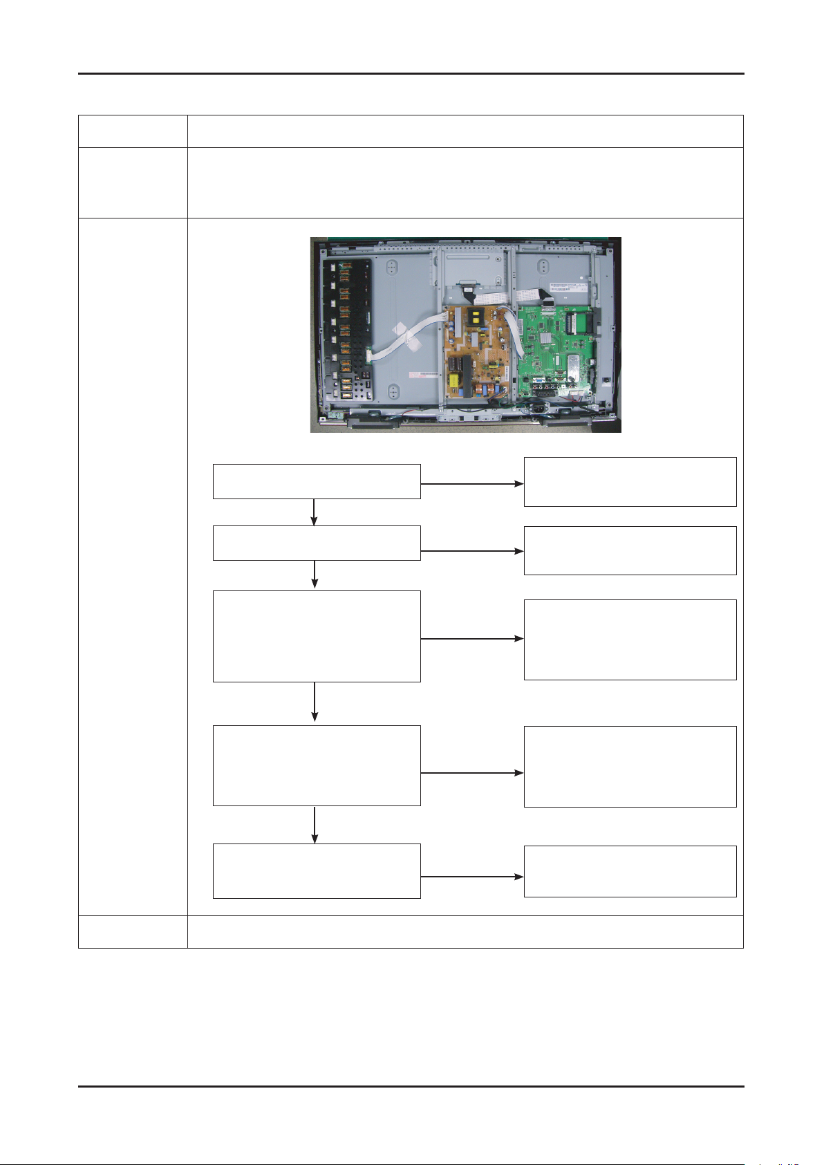
4. Troubleshooting
4-1-2. No Power
-
Symptom
Major
checkpoints
-
-
The IP relay or the LEDs on the front panel does not work when connecting the power cord if the cables are
improperly connected or the Main Board or SMPS is not functioning. In this case, check the following:
-
-
-
-
The LEDs on the front panel do not work when connecting the power cord.
The SMPS relay does not work when connecting the power cord.
The units appears to be dead.
Check the internal cable connection status inside the unit.
Check the fuses of each part.
Check the output voltage of SMPS.
Replace the Main Board.
Diagnostics
Lamp(Backlight) Off,
power indicator LED on?
Yes
Does proper Stand-By DC
A5V_PW appear at TP2004?
Yes
Does proper Main B12VS_PW,
B13V_PW, B5V_PW appear at
TP2007~8, TP2020~2, TP2013~6?
Yes
Does proper A3.3V_PW
appear at R2028?
Yes
Does proper B3.3V_PW, B1.9V_PW,
B1.25V_PW appear at
C2607, C2590, C2105?
Yes
Does proper PANEL_VCC_PW
appear at LVDS connector Pin #1~5
of T-con b’d?
Yes
No
No
No
No
No
No
Change the 30P power cable
or IP board
Change the Main Assy
Change the LVDS cable
4-2
Caution
Does proper DC B12V
appear at F1 of T-con b’d?
Yes
A power is supplied to set?
Make sure to disconnect the power before working on the IP board.
No
No
Change the T-con b’d
Check a other function
(No picture part)
Replace a LCD Panel
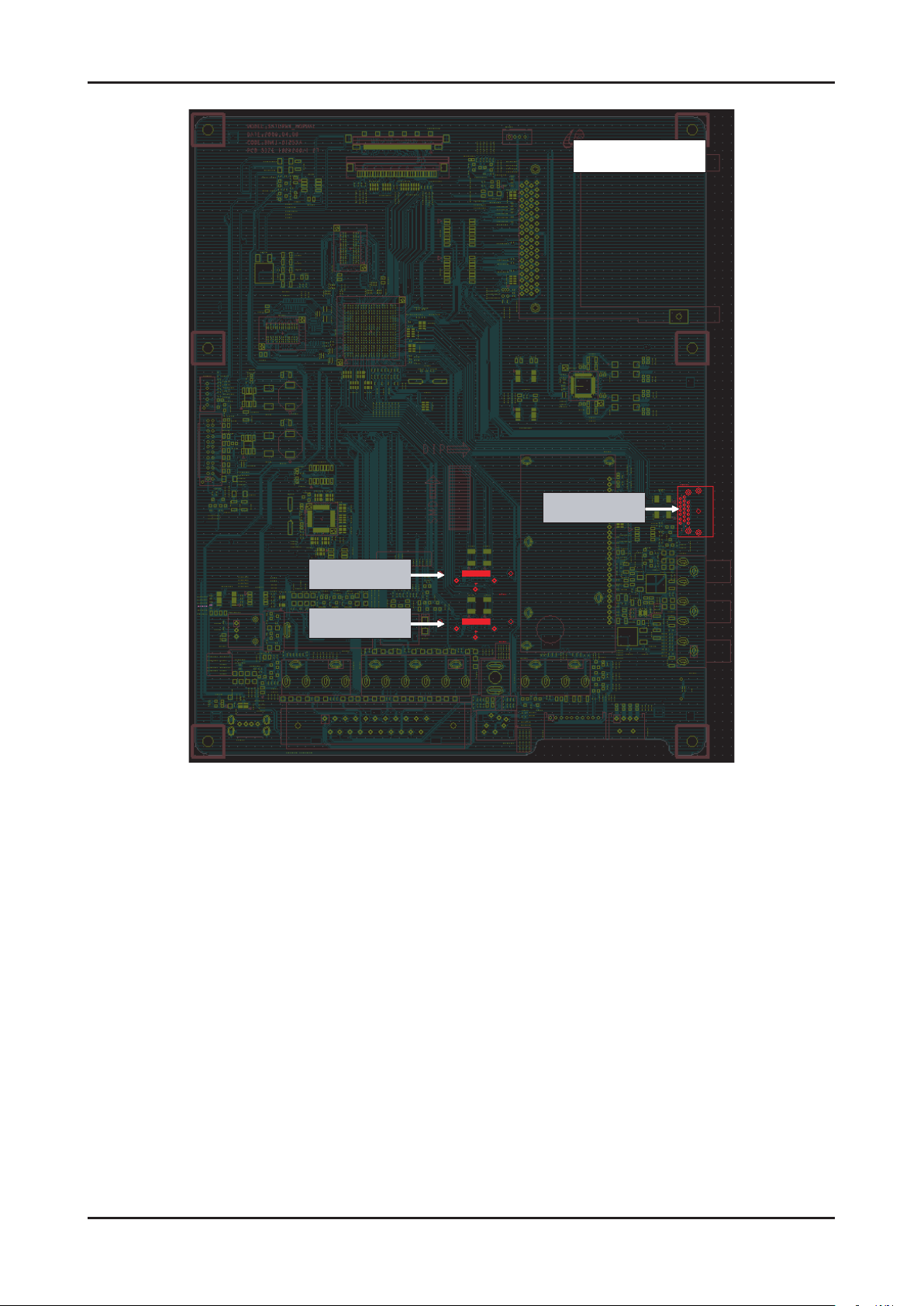
Page 21
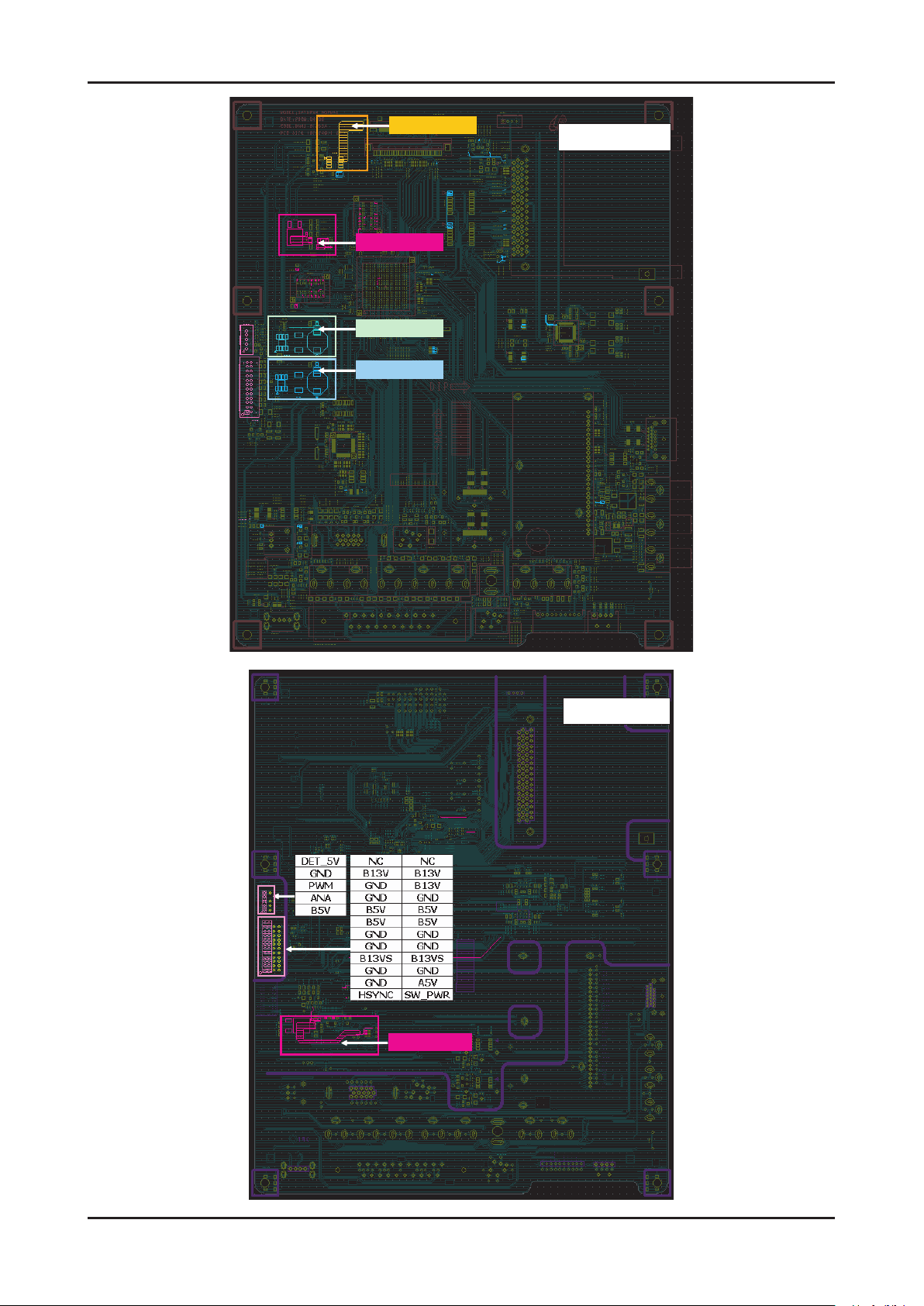
4. Troubleshooting
TOP
B3.3V_PW
B1.25V_PW
B1.25V_PW
PANEL_PW
BOTTOM
A3.3V_PW
4-3
Page 22
4. Troubleshooting
4-1-3. No Video (Analog PC signal)
Symptom Audio is normal but no picture is displayed on the screen.-
Check the PC source
Major
checkpoints
-
Check the Arsenal, Check the Chelsea.
-
This may happen when the LVDS cable connecting the Main Board and the Panel is disconnected.
-
Diagnostics
Power indicator LED is off.
Lamp(Backlight) on, no video
Yes
Check the PC source and
check the connection of D-SUB
Yes
Does the signal appear at TP5002,
1
2
5003, 5004, 5006, 5008?
Yes
Does the digital data appear at
Pin #19,20,34,35 (LVDS Data clk)
of LVDS connector?
Yes
Check the LVDS cable?
Check the T-Con B’d?
Replace the LCD panel?
No
No
No
No
No
Check a set
in the ‘Stand-by mode’ or
‘DPMS mode’
Input the analog
PC signal properly.
Check CN5001, PC cable.
Change the Main Assy
Check IC4010 (Saturn4)
Change the Main Assy
Please, Contact Tech support.
Caution Make sure to disconnect the power before working on the IP board.
4-4
Page 23
4. Troubleshooting
BOTTOM
LVDS
D-SUB
4-5
Page 24
4. Troubleshooting
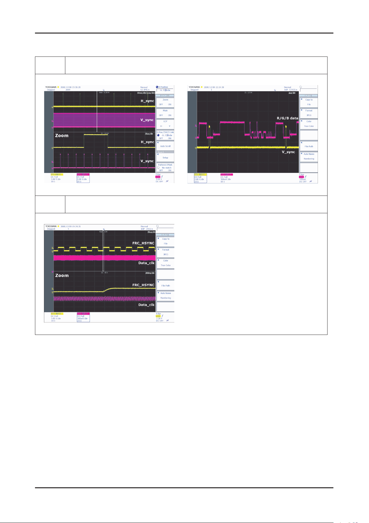
WAVEFORMS
1
2
PC input (V-sink , H-sink , R/G/B)
LVDS output
4-6
Page 25
4-1-4. No Video (HDMI 1, 2, 3 - Digital Signal)
Symptom Audio is normal but no picture is displayed on the screen.-
Check the HDMI source.
Major
checkpoints
-
Check the HDMI switch, Check the Chelsea.
-
This may happen when the LVDS cable connecting the Main Board and the Panel is disconnected.
-
4. Troubleshooting
Diagnostics
Power Indicator is off.
Lamp(Backlight) Off, no video?
Yes
Check the HDMI source and check
the connection of HDMI cable?
Yes
Does the signal appear at
3
2
CN6009 (Pin#12 , #7 )(HDMI1)
CN6002 (Pin#12 , #7 )(HDMI2)
CN6004 (Pin#12 , #7 )(HDMI3)
(HDMI RX_Clk , RX_Data)?
Yes
Does the digital data appear at
Pin #19,20,34,35 (LVDS Data clk)
of LVDS connector?
Yes
Check the LVDS cable?
Check the T-Con B’d?
Replace the LCD panel?
No
No
No
No
No
Check a set
in the ‘Stand-by mode’.
Input the HDMI signal properly
Check CN6009, CN6002, CN6004
Check HDMI cable
Change the Main Assy
Check IC4010 (Saturn4)
Change the Main Assy
Please, Contact Tech support
Caution Make sure to disconnect the power before working on the IP board.
4-7
Page 26
4. Troubleshooting
HDMI1
HDMI2
HDMI3
TOP
4-8
Page 27
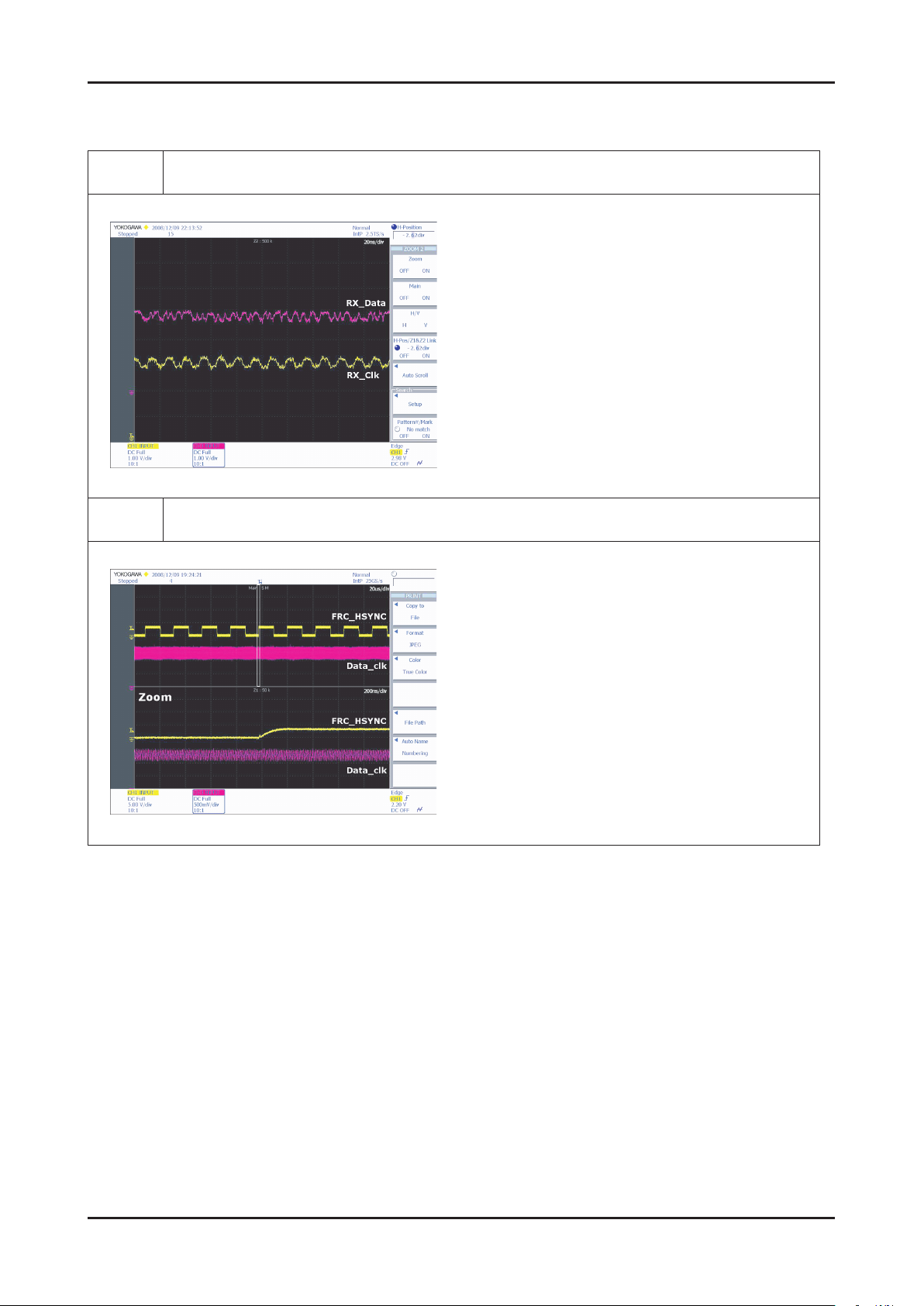
WAVEFORMS
4. Troubleshooting
3
2
HDMI input (RX_Data, RX_Clk)
LVDS output
4-9
Page 28

4. Troubleshooting
4-1-5. No Video (Tuner_CVBS)
Symptom Audio is normal but no picture is displayed on the screen.-
Check the Tuner CVBS source.
Major
checkpoints
-
Check the Tuner, Check the Chelsea.
-
This may happen when the LVDS cable connecting the Main Board and the Panel is disconnected.
-
Diagnostics
Power indicator LED is off.
Lamp(Backlight) on, no video?
Yes
Check the RF source and
check the connection of RF cable?
Yes
Does the DC TU5V_PW, TU33V_PW
appear at #3, #5 Pin of Tuner?
Yes
4
2
Does the CVBS data appear at
#9 pin of Tuner?
Yes
Does the digital data appear at
Pin #19,20,34,35 (LVDS Data clk)
of LVDS connector?
Yes
No
No
No
No
No
Check a set
in the ‘Stand-by mode’.
Input the RF source properly.
Change the Main Assy
Check Tuner
Change the Main Assy
Check IC4010 (Saturn4)
Change the Main Assy
Check the LVDS cable?
Check the T-Con B’d?
Replace the LCD panel?
Caution Make sure to disconnect the power before working on the IP board.
No
4-10
Please, Contact Tech support
Page 29

4. Troubleshooting
TUNER
TOP
4-11
Page 30

4. Troubleshooting
WAVEFORMS
CVBS OUT (Grey Bar)
4
LVDS output
2
4-12
Page 31

4-1-6. No Video (Tuner DTV)
Symptom Audio is normal but no picture is displayed on the screen.-
Check the DTV source.
Major
checkpoints
-
Check the Tuner, Check the Chelsea.
-
This may happen when the LVDS cable connecting the Main Board and the Panel is disconnected.
-
4. Troubleshooting
Diagnostics
Power indicator LED is off.
Lamp(Backlight) on, no video
Yes
Check the connection of RF cable
Yes
Check the ‘signal strength’
in Self Diagnosis menu
Strength is enough?
Yes
Does the DC B5V_VCCT_PW,
B1.25VT_PW, B3.3V_PW
appear at #3, #15, #12 Pin of Tuner?
Yes
Does the digital data appear at
Pin #19,20,34,35 (LVDS Data clk)
2
of LVDS connector?
Yes
No
No
No
No
No
Check a set
in the ‘Stand-by mode’.
Input the RF cable properly.
Check the D-TV source.
Change the Main Assy
Check IC4010 (Saturn4)
Change the Main Assy
Check the LVDS cable?
Check the T-Con B’d?
Replace the LCD panel?
Caution Make sure to disconnect the power before working on the IP board.
No
Please, Contact Tech support
4-13
Page 32

4. Troubleshooting
TUNER
TOP
4-14
Page 33

WAVEFORMS
4. Troubleshooting
2
LVDS output
4-15
Page 34

4. Troubleshooting
4-1-7. No Video (Video CVBS)
Symptom Audio is normal but no picture is displayed on the screen.-
Check the Video CVBS source
Major
checkpoints
-
Check the Chelsea.
-
This may happen when the LVDS cable connecting the Main Board and the Panel is disconnected.
-
Power indicator LED is off.
Lamp(Backlight) on, no video?
Yes
Diagnostics
4
2
Caution Make sure to disconnect the power before working on the IP board.
Check the video source and
check the connection of video cable?
Yes
Does the CVBS data appear at
TP - 7045?
Yes
Does the digital data appear at
Pin #19,20,34,35 (LVDS Data clk)
of LVDS connector?
Yes
Check the LVDS cable?
Check the T-Con B’d?
Replace the LCD panel?
No
No
No
No
No
Check a set
in the ‘Stand-by mode’.
Input the video source properly.
Check CN7005
Change the Main Assy
Check IC4010 (Saturn4)
Change the Main Assy
Please, Contact Tech support
4-16
Page 35

4. Troubleshooting
Side-AV
AV2_CVBS
BOTTOM
4-17
Page 36

4. Troubleshooting
WAVEFORMS
CVBS OUT (Grey Bar)
4
LVDS output
2
4-18
Page 37

4-1-8. No Video (Component)
Symptom Audio is normal but no picture is displayed on the screen.-
Check the Component source
Major
checkpoints
-
Check the chelsea.
-
This may happen when the LVDS cable connecting the Main Board and the Panel is disconnected.
-
4. Troubleshooting
Diagnostics
Power indicator LED is off.
Lamp(Backlight) on, no video?
Yes
Check the component source and
check the connection of
component cables(Y,Pb,Pr)?
Yes
Does the component data appear at
5
2
TP - 5100, 5024, 5025
(Comp1 / Y, Pb, Pr)?
Yes
Does the digital data appear at
Pin #19,20,34,35 (LVDS Data clk)
of LVDS connector?
Yes
Check the LVDS cable?
Check the T-Con B’d?
Replace the LCD panel?
No
No
No
No
No
Check a set
in the ‘Stand-by mode’.
Input the component
source properly.
Check CN5003
Change the Main Assy
Check IC4010 (Saturn4)
Change the Main Assy
Please, Contact Tech support
Caution Make sure to disconnect the power before working on the IP board.
4-19
Page 38

4. Troubleshooting
COMPONEN T
YPbPr
BOTTOM
4-20
Page 39

WAVEFORMS
4. Troubleshooting
5
2
Compnent_Y (Gray scale) / Pb / Pr (Color bar)
LVDS output
4-21
Page 40

4. Troubleshooting
4-1-9. No Sound
Symptom Video is normal but there is no sound..-
Major
checkpoints
-
-
-
When the speaker connectors are disconnected or damaged.
When the sound processing part of the Main Board is not functioning.
Speaker defect..
Check the source and
check the connection of sound cable
(Comp/PC/DVI to HDMI).
Yes
No
Input the sound source properly.
Diagnostics
7
Caution Make sure to disconnect the power before working on the IP board.
Does the sound data appear at
CN5002(COMP), CN5011(PC, DVI),
CN7005(AV), JA3201_EU(SCART)?
Yes
Does the B12VS_PW
appear at TP2007~8?
Yes
Does the sound data appear at
TP - L-, L+, R-, R+?
Yes
Replace speaker
No
No
No
No
Check CN5002(COMP), CN5011
(PC, DVI), CN7005(AV), JA3201_
EU(SCART) Change the Main Assy
Change the Main Assy
Check IC4010 (Saturn4)
Check IC9002 (Sound AMP)
Change the Main Assy
Please, Contact Tech support
4-22
Page 41

4. Troubleshooting
Side-AV
SCART
PC audio
COMPONENT
BOTTOM
TOP
Sound AMP
Speaker out
4-23
Page 42

4. Troubleshooting
WAVEFORMS
I2C Data
6
Speaker out
7
4-24
Page 43

4-2. Alignments and Adjustments
4-2-1. General Alignment Instuction
Usually, a color LCD-TV needs only slight touch-up adjustment upon installation.
1.
Check the basic characteristics such as height, horizontal and vertical sync.
Use the specied test equipment or its equivalent.
2.
Correct impedance matching is essential.
3.
Avoid overload. Excessive signal from a sweep generator might overload the front-end
4.
of the TV. When inserting signal markers, do not allow the marker generator to distort test result.
Connect the TV only to an AC power source with voltage and frequency as specied on
5.
the backcover nameplate.
Do not attempt to connect or disconnect any wire while the TV is turned on. Make sure
6.
that the power cord is disconnected before replacing any parts.
To protect against shock hazard, use an isolation transformer.
7.
4. Troubleshooting
4-25
Page 44

4. Troubleshooting
4-3. Factory Mode Adjustments
4-3-1 Entering Factory Mode
To enter ‘Service Mode’ Press the remote -control keys in this sequence :
- If you do not have Factory remote - control
INFOPower OFF MENU MUTE
4-3-2 How to Access Service Mode
Using the Customer Remote
Turn the power off and set to stand-by mode
1.
Press the remote buttons in this order; POWER OFF- INFO - MENU - MUTE to turn the set on.
2.
The set turns on and enters service mode. This may take approximately 20 seconds.
3.
Press the Power button to exit and store data in memory.
4.
- If you fail to enter service mode, repeat steps 1 and 2 above.
Initial SERVICE MODE DISPLAY State
5.
OPTION
ADC/WB
Control
Advanced
Expert
T-CRLPEUC-XXXX
T-CRLPEUFC-XXXX
T-CRLPEUS-XXXX
DTP-LP-XXXX-XX
DTP-LP-App-XXXX-XX
OPTION : F100 00
ADC : HDMI X COMP X PC X AV X
EDID : SUCCESS
HDCP : SUCCESS
Current Flash : Flash X
Build Date : XX-XX-XXXX
Date Of Purchase : XX/XX/XX
* How to enter the hidden factory mode.
a. into the factory mode
b. move the tap to Advanced
c. key input : 0 + 0 + 0 + 0
** hidden menu : Advanced
6. Buttons operations withn Service Mode
Menu Full Menu Display/Move to Parent Menu
Direction Keys /
Direction Keys /
Source
Item Selection by Moving the Cursor
Data Increase / Decrease for the Selected Item
Cycles through the active input source that are connected to the unit
4-26
Page 45

4-3-3 Factory Data
4. Troubleshooting
OPTION
ADC/WB
Factory Name Data Range
Factory Reset
Type 32L6AF1C 19D6THOC, 19I6THOC… (PANEL, INCH)
Model LB530 LB530 / LB540 / LB550 / LB460 / LB360 / LB650 / LB530S
TUNER Auto Auto/Sem_SL/Alps_SL/Sem_TC
Region EU EU/ND/ASIA/CHN
DDR SAMSUNG SAMSUNG / Etron
Light Effect Off On / Off
CH Table SUWON SUWON, SESK…(Factory Channel Type)
Medialink Type
Local Set Others Others/Russia
PDP GROUP
Factory Name
ADC
ADC Tarhet
ADC RESULT
WB
ADC
ADC Target
Factory Name Data Range
AV Calibration
Comp Calibration
PC Calibration
HDMI Calibration
Factory Name Data Range
1st_AV_Low
1st_AV_High
1st_AV_Delta
1st_COMP_Low
1st_COMP_High
1st_COMP_Delta
1st_PC_Low
1st_PC_High
1st_PC_Delta
2nd_Low
2nd_High
2nd_Delta
Success
Success
Success
Success
18
220
1
16
235
1
2
235
1
1
235
1
Success / Failure
Success / Failure
Success / Failure
Success / Failure
0 ~ 255
0 ~ 255
0 ~ 255
0 ~ 255
0 ~ 255
0 ~ 255
0 ~ 255
0 ~ 255
0 ~ 255
0 ~ 255
0 ~ 255
0 ~ 255
4-27
Page 46

4. Troubleshooting
ADC RESULT
Factory Name
1st_AV_Gain
1st_AV_Offset
1st_Comp_Gain
1st_Comp_Gain_Cb
1st_Comp_Gain_Cr
1st_Comp_Offset
1st_Comp_Offset_Cb
1st_Comp_Offset_Cr
1st_PC_R_Gain
1st_PC_G_Gain
1st_PC_B_Gain
1st_PC_R_Offset
1st_PC_G_Offset
1st_PC_B_Offset
2nd_R_Offset
2nd_G_Offset
2nd_B_Offset
2nd_R_Gain
2nd_G_Gain
2nd_B_Gain
AV / RF Component
136
136
136
107
107
107
136
136
136
107
136
136
136
107
107
107
136
136
136
107
134
134
134
67
67
67
134
134
134
67
134
134
134
67
67
67
134
134
134
67
Mode
HDMI / DTV /
HDMI-PC
136
136
136
100
100
100
136
136
136
100
136
136
136
100
100
100
136
136
136
100
PC
192
192
192
32
32
32
192
192
192
32
192
192
192
32
32
32
192
192
192
32
Range
0 ~ 255
0 ~ 255
0 ~ 255
0 ~ 255
0 ~ 255
0 ~ 255
0 ~ 255
0 ~ 255
0 ~ 255
0 ~ 255
0 ~ 255
0 ~ 255
0 ~ 255
0 ~ 255
0 ~ 255
0 ~ 255
0 ~ 255
0 ~ 255
0 ~ 255
0 ~ 255
WB
Factory Name
Sub Brightness
R_Offset
G_Offset
B_Offset
Sub Contrast
R_Gain
G_Gain
B_Gain
Movie R Offset
Movie B Offset
Movie R Gain
Movie B Gain
Mode
AV Component HDMI / DTV PC
128
512
512
512
128
512
512
512
128
512
512
512
128
512
512
512
128
512
512
512
128
512
512
512
128
512
512
512
128
512
512
512
128
512
512
512
128
512
512
512
128
512
512
512
128
512
512
512
4-28
Page 47

4. Troubleshooting
Control
EDID
Factory Name
EDID
Sub Option
PDP Option
Hotel Option
Shop Option
Sound
Cong Option
Factory Name Data Range
EDID ON/OFF
EDID WRITE ALL
EDID WRITE PC
EDID WRITE DVI
EDID WRITE HDMI1
EDID WRITE HDMI2
EDID WRITE HDMI3
EDID WRITE HDMI4
EDID VERSION
Off
Success
Success
Success
Success
Success
Success
Failure
HDMI 1.3
Success / Failure
Success / Failure
Success / Failure
Success / Failure
Success / Failure
Success / Failure
Success / Failure
HDMI 1.2 / HDMI 1.3
On / Off
4-29
Page 48

4. Troubleshooting
Sub
Option
Factory Name Data Range
Mute Time(VIDEO)
ready
TTX LIST
TTX
TTX Group
Hotplug
Hotplugcontrol
Spread Spectrum
Auto Power
Arab
NT Conversion
Mirror
HDMI EQ1
HDMI EQ2
HDMI EQ3
HDMI EQ4
EER Count
WM Calib
Panel Enter Key
Panel Display Time
CHECKSUM
View Log
Font Data Viewer
Dimm Type
Gamma
Carrier Mute
Anynet+
HPD Polarity
High Devi
Volum Curve
HotPlug Delay
HP Ident
PC Ident
Info Live
Watchdog
LVDS Format
OSD Resolution
Bus Stop
OTA Code
Panel Auto Setting
OTA Duration Test
Alternate Del
4
Failure
FLOF
On
Lang OSD
On
On
On
Off
Off
Off
Middle
Middle
Middle
Middle
XHr
0x0000
INT_NEG
0.95
Off
On
Off
EU
9
Low
On
On
JEIDA
1920*1080
0 ~ 10
Success / Failure
FLOF / LIST
On / Off
Lang OSD/ W Europe/E Europe/Russia/Greek/Turkey/Arab/Farsi/ArabHbrw
On / Off
On / Off
On / Off
On / Off
On / Off
On / Off
Low / Middle / High / Strong
Low / Middle / High / Strong
Low / Middle / High / Strong
Low / Middle / High / Strong
INT / EXT / INT_NEG / INT_POS / EXT_NEG
Off / 0.85 / 0.88 / 0.90 / 0.93 / 0.95 / 0.98
On / Off
On / Off
On / Off
NT / EU / EA
0 ~ 63
Low / High
On / Off
On / Off
JEDIA / VESA
4-30
Page 49

Spread Spectrum
Factory Name Data Range
Spread Spectrum
Step1
Step2
Range1
Range2
DDR Spread
On
149
0
215
0
2% Spread
On / Off
0~255
0~3
0~255
0~4
Off / 1% Spread / 2% Spread
4. Troubleshooting
PDP Option
Hotel Option
Factory Name Data Range
PIXEL SHIFT TEST
LOGIC CONNECT
PATTERN SELECT
PANEL VERSION
PANEL INCH
PANEL TYPE
PANEL TEMPERATURE
LOGIC SW VERSION
LOGIC SW CHECKSUM
SAPC_Timer
APC_Speed
LOGIC USB D/L
Factory Name Data Range
Hotel Mode
Power On Channel
Power On Source
Power On Volume
Min Volume
Max Volume
Panel Button Lock
Pic Menu Lock
Music Mode (AV)
Music Mode (PC)
Music Mode (Comp)
Music Mode Backlight
Menu Display
Power On Option
Ch Remap On/Off
Program Ch
Original Ch/Src
Auto PC
Energy Saving
Cloning : TV to USB
Cloning : USB to TV
Welcome Message
Off
Off
0
On
Slow
Failure
Off
3
TV
10
0
100
Off
Off
Off
Off
Off
Off
On
Last Option
Off
Off
On / off
On / off
0 ~ 31
On / off
Slow / Fast
Not Match / Match / Failure
TV / S-Video / Comp1 / PC / HDMI1 / HDMI2 / HDMI4
Standby / Power On / Last Option
Off / Low / Mid / High / Auto
On / Off
On / Off
On / Off
On / Off
On / Off
On / Off
On / Off
On / Off
On / Off
4-31
Page 50

4. Troubleshooting
Shop Option
Sound
Factory Name Data Range
Shop Mode
USB DEMO ON (SEC)
USB DEMO OFF (SEC)
Factory Name Data Range
FM Prescale
AM Prescale
Nicam Prescale
A2 M2S Threshold
A2 S2M Threshold
A2 PilotPhaseOn
A2 PilotPhaseOff
A2 Identon
A2 Identoff
A2 Carr1AmpOnThr
A2 Carr1AmpOffThr
A2 Carrier1SNRonThr
A2 Carrier1SNRoffThr
A2 Carr2AmpOnThr
A2 Carr2AmpOffThr
A2 Carrier2SNRonThr
A2 Carrier2SNRoffThr
Nicam Sig Error On
Nicam Sig Error Off
Compression mode
Dolby Test Mode
DTV Level
Master Vol
PWM Modulation
DRC1 Threshold
DRC2 Threshold
Speaker EQ
SC1 Vol
SC2 Vol
Audio Delay
SUB AMP Master Vol
SUB AMP PWM Mod
SUB DRC Thresh
SUB Speaker EQ
Off On / Off
68
49
72
0x02
0x01
0x10
0x1E
0x02
0x00
0x04
0x02
0x15
0x7F
0x08
0x03
0x10
0x18
0x23
0x3F
RF
off
-12dB
32
254
0x35
0x23
On
16
16
60
Cong Option
4-32
Factory Name Data Range
Number of AV
Number of SVIDEO
Number of COMP
Number of HDMI
Number of SCART
DVI Sound
Headphone
Number of USB PORT
LNA SUPPORT
MFT OFFSET
1
0
1
3
1
0
0
off
0 ~ 2
0 ~ 1
0 ~ 2
0 ~ 4
0 ~ 2
0 ~ 1
0 ~ 1
On / Off
Page 51

4. Troubleshooting
Advanced
WB
Movie
Factory Name
FBE
WB Movie
EPA Standard
ADJUST
YC_Delay
SHARPNESS
PE
PQ Others
Color Space
EEPROM RESET
Factory Name Data Range
WB Movie
Color Mode
Color Tone
Msub Brigh
Msub Contr
W1_RGAIN
W1_BGAIN
W1_ROFFS
W1_BOFFS
W2_RGAIN
W2_BGAIN
W2_ROFFS
W2_BOFFS
N_RGAIN
N_BGAIN
N_ROFFS
N_BOFFS
Movie Contr
Movie Brigh
Movie Color
Movie Sharp
Movie Tint
Movie BkLight
M.Gamma
M_Sub Gamma
Off
---
---
---
---
---
---
---
---
---
---
---
---
---
---
---
---
---
---
---
---
---
---
---
---
On / Off
Dynamic / Standard / Movie
Cool / Normal / Warm1 / Warm2
0 ~ 255
0 ~ 255
0 ~ 255
0 ~ 255
0 ~ 255
0 ~ 255
0 ~ 255
0 ~ 255
0 ~ 255
0 ~ 255
0 ~ 255
0 ~ 255
0 ~ 255
0 ~ 255
3 ~ 100
2 ~ 100
1 ~ 100
0 ~ 100
0 ~ 50
0 ~ 10
Off / 0.85 / 0.88 / 0.90 / 0.93 / 0.95 / 0.98 / M1 / M2 / M3 / M4
-3 ~ +3
4-33
Page 52

4. Troubleshooting
EPA Standard
ADJUST
Factory Name Data Range
Std Contr
Std Bright
Std Sharp
Std Color
Std Tint
Std Backlight
Factory Name Data Range
Dynamic Dimming
LNA Plus
Power Key Protect
Uart Select
Debug Mode
Back End Mute
PDP FRC
Visual Test
Standby Mode Time
Delete alt.ver
OTA conrm Time
OTA limit Time
Dynamic CE
FWC
1080p 48Hz
PWM Max
Quick Start
DTV LNA
HDCP Download
Test Pattern
Off
Off
Auto Wall
Debug Off
Disable
45 Min
2 Flash
90 Min
3 Hour
Off
Off
On
100
Auto
On
Off
95
45
50
50
50
8
Debug Off / Debug Smart / Debug RunTime
0 ~ 100
0 ~ 100
0 ~ 100
0 ~ 100
0 ~ 100
0 ~ 10
On / Off
On / Off
Auto Wall / Debug / MDC / On1 / On2
Disable / Enable
2 Min / 45 Min
2 Min / 90 Min
3 Min / 3 Hour
On / Off
On / Off
On / Off
1 ~ 100
Auto / On / Off
On / Off
Off / 1 ~ 13
LNA Plus
YC_Delay
Factory Name Data Range
RF dB1 Level
RF dB2 Level
RF dB3 Level
RF dB4 Level
Factory Name Data Range
PAL BG
PAL DK
PAL I
SECAM BG
SECAM DK
SECAM L
NTSC 358
NTSC 443
AV PAL
AV SECAM
AV NT358
AV NT443
AV PAL60
1
1
1
4
4
5
1
1
1
5
1
1
1
4
6
8
14
0 ~ 255
0 ~ 255
0 ~ 255
0 ~ 255
0 ~ 3
0 ~ 3
0 ~ 3
0 ~ 7
0 ~ 7
0 ~ 7
0 ~ 3
0 ~ 3
0 ~ 3
0 ~ 7
0 ~ 3
0 ~ 3
0 ~ 3
4-34
Page 53

4. Troubleshooting
SHARPNESS
SHARPNESS
Factory
Name
H1 Gain
H2 Gain
H3 Gain
H4 Gain
V1 Gain
V2 Gain
H overshoot
V overshoot
H undershoot
V undershoot
Coring TH2
Coring TH1
Comp/HDMI/
DTV 720p
20
8
8
8
20
8
FF
20
FF
20
1
1
Data
Data Range component HDMI DTV
RF CVBS SD
25
12
10
8
20
12
20
20
20
20
1
1
Data
25
12
10
8
20
12
20
20
20
20
1
1
PC / HDMI
PC
8
8
8
8
8
8
0
0
0
0
0
0
25
12
C
20
12
20
20
20
20
8
1
1
HD
(720p)
20
8
8
8
20
8
FF
20
FF
20
1
1
Range
0 ~ 3F
0 ~ 3F
0 ~ 3F
0 ~ 3F
0 ~ 3F
0 ~ 3F
0 ~ FF
0 ~ FF
0 ~ FF
0 ~ FF
0 ~ F
0 ~ F
SD
25
12
8
8
20
12
20
20
20
20
1
1
HD
(720p)
20
8
8
8
20
8
FF
20
FF
20
1
1
SD
25
12
C
8
20
12
20
20
20
20
1
1
HD
(720p)
20
8
8
8
20
8
FF
20
FF
20
1
1
PE
Factory Name
Skin x
Skin y
B_slope
DLC_ML
DLC_MH
DLC_H
Skin_SAT
Skin_HUE
M_Skin_HUE
M_Skin_x
M_Skin_y
Mid_color_level
M_Mid_color_level
RF CVBS
0
0
A0
60
70
EB
0
40
40
0
0
180
180
0
0
A0
60
70
EB
0
40
40
0
0
180
180
Data
component
SD HD
0
0
A0
60
70
EB
0
40
40
0
0
180
180
0
0
A0
60
70
EB
0
40
40
0
0
180
180
HDMI DTV
0
0
A0
60
70
EB
0
40
40
0
0
180
180
0
0
A0
60
70
EB
0
40
40
0
0
180
180
PC /
HDMI PC
0
0
80
60
70
EB
0
0
0
0
0
180
180
Range
0 ~ 11
0 ~ 11
80~FF
0~FF
0~FF
0~FF
0~F
0~7F
0~7F
0 ~ 11
0 ~ 11
0 ~ 255
0 ~ 255
4-35
Page 54

4. Troubleshooting
PQ Others
Color
Space
Factory
Name
Red Sat
Red Hue
Green Sat
Green Hue
Blue Sat
Blue Hue
Cyan Sat
Cyan Hue
Magenta Sat
Magenta Hue
Yellow Sat
Yellow Hue
FWC CB
FWC CR
Factory Name Data Range
7.5 IRE NTSC
7.5 IRE
4
7
A
A
4
2
Comp SD
HDMI SD
DTV SD
4
40
7
7F
A
50
A
50
4
40
2
40
15
15
RF
AV
Native Native Native Auto Auto Auto -
40
7F
50
50
40
40
15
15
Off
16
COMP HD
HDMI HD
DTV HD
4
40
7
7F
A
50
A
50
4
40
2
40
15
15
RF
AV
0
40
0
40
0
40
0
40
0
40
0
40
15
15
On / Off
0 ~ 60
Comp SD
HDMI SD
DTV SD
0
40
0
40
0
40
0
40
0
40
0
40
15
15
COMP HD
HDMI HD
DTV HD
0
40
0
40
0
40
0
40
0
40
0
40
15
15
PC/
HDMI PCRange
Color
Space
0
40
0
40
0
40
0
40
0
40
0
40
15
15
0~F
0~7F
0~F
0~7F
0~F
0~7F
0~F
0~7F
0~F
0~7F
0~F
0~7F
0~30
0~30
EEPROM RESET Factory Name Data
EEPROM RESET Enter - Set off
NVR All Clear Off/On
Tuner Status
(Read Only)
SNR
BER
Signal Strength
Frequency
LNA Status
BandWidth
FFT
Modulation
Code Rate
Gl
Hier Modulation
Frequency Offset
Timing Offset
AGC
UCB
PLL Type
DEMOD Type
TPS Lock
RS Lock
4-36
Page 55

4-4. White Balance - Calibration
4-4-1 White Balance -Calibration
4. Troubleshooting
1. Calibration
AV Calibration
Comp Calibration
PC Calibration
HDMI Calibration
4-4-2 White Balance - Adjustment
(low light) (hight light)
3. W/B
Sub Bright
R offset
G offset
B offset
Sub Contrast
R gain
G gain
B gain
(W/B adjustment Condition refer next page)
4-5. White Ratio (Balance) Adjustment
You can adjust the white ratio in factory mode (1:Calibration, 3:White-Balance).
1.
Since the adjustment value and the data value vary depending on the input source, you have to
2.
adjust these in CVBS, Component 1 and HDMI 1 modes.
The optimal values for each mode are congured by default. (Refer to Table 1, 2)
3.
It varies with Panel’s size and Specication.
- Equipment : CS-210
- Pattern: MIK K-7256 #92 “Flat W/B Pattern” as standard
- Use other equipment only after comparing the result with
that of the Master equipment.
- Set Aging time : 60min
- Calibration and Manual setting for WB adjustment.
HDMI : Calibration at #24 Chessboard Pattern Manual adjustment #92 pattern (720p)
COMP: Calibration at #24 Chessboard Pattern Manual adjustment at #92 pattern (720p)
CVBS: Calibration at #24 Chessboard Pattern Manual adjustment at #92 pattern (PAL)
- If nishing in HDMI mode, adjustment coordinate is almost same in AV/COMP mode.
- White Balance Manual Adjustment
4-37
Page 56

4. Troubleshooting
P-Mode
CVBS
(PAL)
COMP
(720P)
HDMI
(720P)
x y Y (Luminance) T(K) + MPCD
H/L 272 278
L/L 272 278
H/L 272 278
L/L 272 278
H/L 272 278
L/L 272 278
Adjustment Coordinate
-
(Sub_CT:130)
12.6cd/m
(Sub_CT:130)
13.0cd/m
(Sub_CT:130)
13.0cd/m
2
(3.7 Ft)
-
2
(3.8 Ft)
-
2
(3.8 Ft)
12,000 (±0)
12,000 (±0)
12,000 (±0)
12,000 (±0)
12,000 (±0)
12,000 (±0)
- Adjustment Specication
White Balance : High light (±1), Low light (±3)
Luminance : High light (Don’t care), Low light (±0.2 Ft/L)
4-6. Servicing Information
4-6-1 USB Download Method
Samsung may offer upgrades for TV’s rmware in the future. Please contact the Samsung call center at 1-800-
SAMSUNG (726-7864) to receive information about downloading upgrades and using a USB drive. Upgrades will be
possible by connecting a USB drive to the USB port located on your TV.
Insert a USB drive containing the rmware upgrade into the
1.
USB port on the rear of the TV.
Press the MENU button to display the menu.
2.
Press the or button to select “Support”, then press the
ENTER button.
Press the or button to select “SW Upgrade”, then press
3.
the ENTER button.
The message “Scanning for USB. It may take up to 30
seconds.” is displayed.
The message “Upgrade version XXXX to version XXXX?
4.
The system will be reset after upgrade.” is displayed.
Press the or to select the “OK”, then press the ENTER
button.
Please be careful to not disconnect the power or remove the
USB drive while upgrades are being applied. The TV will turn off
and turn on automatically after completing the rmware upgrade.
Please check the rmware version after the upgrades are
complete. When software is upgraded, video and audio settings
you have made will return to their default (factory) settings.
We recommend you write down your settings so that you can
easily reset them after the upgrade.
4-38
Page 57

4-7. S/W UPDATE MANUAL (use ISP TOOL & JIG)
Order Description
Connect Mstar JIG to the TV Set with
1
D-SUB cable.
Enter the factory mode and Check the
2
Flash of current S/W.
4. Troubleshooting
Open the Flash Downloader.
3
(ISP TOOL)
Select the ‘Read’ Tab and Choose the
4
S/W. (merge.bin)
4-39
Page 58

4. Troubleshooting
Order Description
Select the ‘Connect’ Tab and Check
5
the Device Type Message.
Select the ‘Device’ Tab and
6
Check ‘WP Pin pull to high during
ISP’.
Select the ‘Auto’ Tab and Check
‘Multi Flashes’. After you can see the
7
“SpiFlash_X” menu. Check the same
Flash no. that Current Flash
on factory menu.
8 Check all process and push ‘Run’.
4-40
Page 59

Order Description
Check the Verify OK,
9
and ‘PASS’ message.
4. Troubleshooting
10
Select the ‘Dis Con’ Tab
And disconnect the JIG.
4-41
Page 60

4. Troubleshooting
4-8. Mechanical diagram
Set Size
(With stand)
Set Size
(W/O stand)
Opening Size 699 x 393.8
USA
Packing Size
ETC
Net(Set) Weight
(With Stand)
Net(Set) Weight
(W/O Stand)
Gross Weight
(After Packing)
USA -
EUR 12.86
USA -
EUR 10.88
USA -
EUR 16.7
KOR -
801.0*220.2*562.5
801.0*87.7*518.1
905*615*200KOR
4-42
Page 61

5. Exploded View & Part List
T0003
M0027
M0013
M0115
T0764
T0522
M0014
M0254
M0107
M0215
T0447
5-1. LE32B53*P7N Exploded View
5. Exploded View & Part List
5-1
Page 62

5. Exploded View & Part List
5-1-1. LE32B53*P7N Parts List
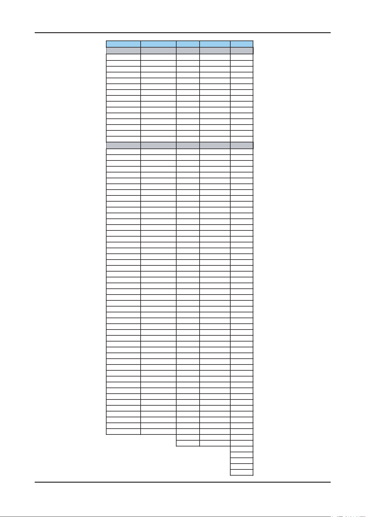
Location No. Code No. Description & Specication Q’ty S.A/S.N.A Remark
T0003 BN96-09658R ASSY COVER P-FRONT;LB530 32,EO(08),ABS+P 1 S.A
M0013 BN96-06947G ASSY COVER P-REAR;LB530 32,EO(08),HIPS,H 1 S.A
M0215
T0447 BN96-04681G ASSY BRACKET P-PANEL;-,32R81,-,-,-,-,CMO 1 S.N.A
M0014 BN94-02665A ASSY PCB MAIN;PN58B850Y1FXZA 1 S.A
M0107 BN63-03039A SHIELD-COVER;MURANO40,PCM,T0.5,IDTV 1 S.A
T0764
M0254 BN61-05651A HOLDER-SIDE AV;08’ PANEL,HIPS,BK500,HB, 1 S.N.A
T0522 BN96-06818B ASSY SPEAKER P-ASSY SPEAKER P;8ohm,CORAL 1 S.A
M0115 BN61-03706A BRACKET-STAND LINK;BRACKET-STAND-LINK 32 1 S.N.A
M0027 BN96-09131A ASSY STAND P-BASE;LB530 32,ABS+PMMA,HB,B 1 S.A
BN07-00512A
BN07-00574A
BN44-00216A
BN44-00234A
LCD-PANEL;T315HW01 V0
LCD-PANEL; LTF320HA03
SMPS-LCDTV;MK37P5T,SEM,AC/DC,171W,AC100~
SMPS-LCD TV;MK37P6,DYREL
1 S.A
1 S.A
5-2
Page 63

5. Exploded View & Part List
5-2. LE32B53*P7N Parts List
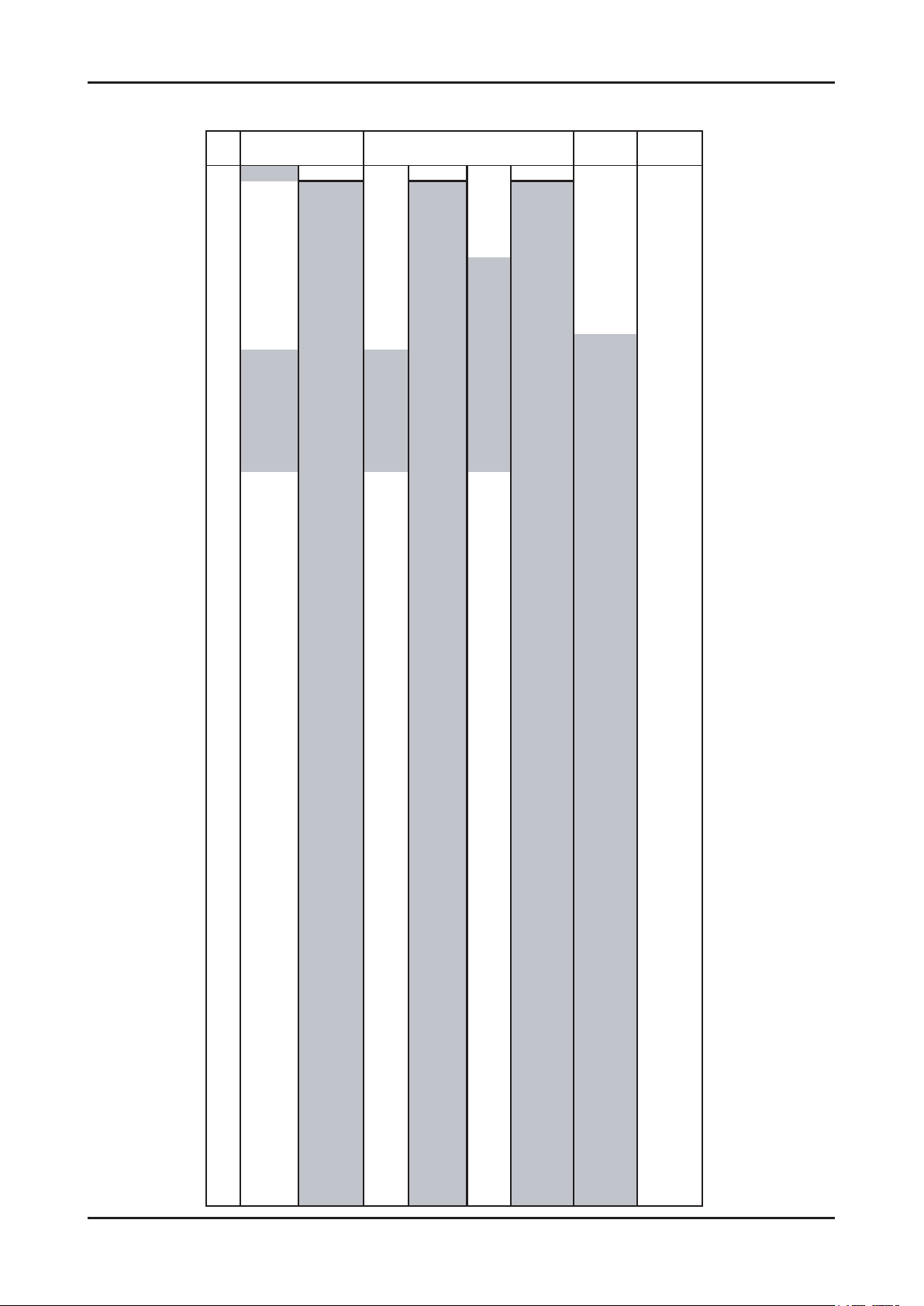
Level Location No. Code No. Description & Specication Q’ty SA/SNA Remark
LE32B530P7NXXC LE32B530P7N,N65E/32AP7-G5P,32,LCD-TV,SPA
0.1 M0002 BN90-01550H ASSY COVER REAR;LB530 32(08) 1 S.N.A
..2 T0081 6002-001294 SCREW-TAPPING;BH,+,,M4,L16,ZPC(BLK) 1 S.N.A
..2 T0081 6002-001294 SCREW-TAPPING;BH,+,,M4,L16,ZPC(BLK) 11 S.N.A
..2 T0081 6002-001294 SCREW-TAPPING;BH,+,,M4,L16,ZPC(BLK) 1 S.N.A
..2 M0013 BN96-06947G ASSY COVER P-REAR;LB530 32,EO(08),HIPS,H 1 S.A
...3 BR/WALL+C/ 6003-001188 SCREW-TAPTYPE;BH,+,-,B,M4,L10,ZPC(WHT),S 4 S.N.A
...3 T0101 BN61-03348A BRACKET-WALL;LCD TV 32,SECC T1.2 4 S.N.A
...3 M0006 BN63-04366F COVER-REAR;L530 32,EO,HIPS,HB,BK500 1 S.N.A
...3 T0071 BN64-01134A INLAY-TERMINAL;LA530,EO,PS SHEET,T0.5,BL 1 S.N.A
0.1 M0001 BN90-01949K ASSY COVER FRONT;LB530 32 1 S.N.A
..2 T0522 BN96-06818B ASSY SPEAKER P-ASSY SPEAKER P;8ohm,CORAL 1 S.A
..2 T0003 BN96-09658R ASSY COVER P-FRONT;LB530 32,EO(08),ABS+P 1 S.A
...3 IR-PCB+H/B 6003-001188 SCREW-TAPTYPE;BH,+,-,B,M4,L10,ZPC(WHT),S 1 S.N.A
...3 K/C+C/F 6003-001188 SCREW-TAPTYPE;BH,+,-,B,M4,L10,ZPC(WHT),S 2 S.N.A
...3 T0069 AA60-00091J SPACER-FELT;FELT,330X10,BLK,T0.5 2 S.N.A
...3 T0069 AA60-00091N SPACER-FELT;FELT,70X10,BLK,T1.0 1 S.N.A
...3 T0069 AA60-00171Q SPACER-FELT;56L3,FELT,690,T0.35,8 2 S.N.A
...3 BN61-04692A BOSS-PRIMER;#94,clear,35cps 0.58 S.N.A
...3 BN63-01925A FELT-VIBRATION;42D5,FELT,T0.35,10,370 2 S.N.A
...3 CCM1 BN63-02183F COVER-SHEET;Rhcm,PE Vinyl,T0.05,900mm,20 2.1 S.N.A
...3 M0112 BN63-04364H COVER-FRONT;LB530 32,EO,ABS+PMMA,HB,BK23 1 S.N.A
...3 CCM1 BN63-04755A COVER-SHEET;AMBER,PE,T0.05,W150mm,200M,6 3 S.N.A
...3 T0059 BN64-00379A INDICATOR LED;ROME-II,23,PC,CLEAR 1 S.N.A
...3 T0061 BN64-00453A WINDOW-REMOCON;32R71,PC,VIOLET 1 S.N.A
...3 T0022 BN64-00755A KNOB-CONTROL;32L450,ABS,V0,BK07 1 S.N.A
...3 BN64-00991B DECORATION-BOTTOM;32,LB530,PC CLEAR,RED 1 S.N.A
...3 BN96-06930B ASSY HOLDER P-BOSS;32L530,HIPS,HB,BK500 1 S.N.A
....4 BN61-03261J BOSS-TAPE;Tulip,ACRYL,T1.1,W16.0mm,GRAY, 0.62 S.N.A
....4 BN61-03885B HOLDER-BOSS BOTTOM;32L530,HIPS,HB,BK500 1 S.N.A
....4 BN61-04692A BOSS-PRIMER;#94,clear,35cps 0.001 S.N.A
...3 M0145 BN96-07269A ASSY BOARD P-FUNCTION;LN40A450C1D,CT5000 1 S.A
...3 M0146 BN96-07270R ASSY BOARD P-POWER & IR;LE32A466C2MXZF,C 1 S.N.A
0.1 M0216 BN90-02228A ASSY STAND;LB530 32,UO(08) 1 S.N.A
..2 BN61-05213A GUIDE-STAND NECK;32,LB530,ABS+PMMA,HB 1 S.N.A
..2 M0027 BN96-09131A ASSY STAND P-BASE;LB530 32,ABS+PMMA,HB,B 1 S.A
...3 T0081 6002-001294 SCREW-TAPPING;BH,+,,M4,L16,ZPC(BLK) 4 S.N.A
...3 C/STANDBOT 6003-001239 SCREW-TAPTYPE;FH,+,B,M4,L10,ZPC(WHT),SWR 6 S.N.A
...3 BN61-02232A HOLDER-SWIVEL RING;32R71,ACETAL NATUAL,N 1 S.N.A
...3 BN61-02233A HOLDER-SWIVEL RING;32R71,ACETAL NATUAL,N 1 S.N.A
...3 BN61-02236A BRACKET-HINGE SWIVEL;BORDEAUX 32,SECC,T1 1 S.N.A
...3 BN61-03707A BRACKET-STAND BOTTOM;PEARL 32,SECC,T2.0 1 S.N.A
...3 BN61-03872A GUIDE-STAND BOTTOM;L450 32INCH,PC+GF(20% 1 S.N.A
....4 BN61-02932B BRACKET-STOPPER NUT;L450,M4,OD8,L24,MOLD 3 S.N.A
...3 CCM1 BN63-02183D COVER-SHEET;Rhcm,PE Vinyl,T0.05,680mm,20 0.4 S.N.A
5-3
Page 64

5. Exploded View & Part List
Level Location No. Code No. Description & Specication Q’ty SA/SNA Remark
...3 T0004 BN63-05520A COVER-STAND BASE;32,LB530,ABS+PMMA,HB 1 S.N.A
...3 M0126 BN73-00052C RUBBER-FOOT;LCD TV,CR RUBBER,T2.0 DIA19, 6 S.N.A
..2 BN96-11175A ASSY COVER P-GUIDE STAND;LB530 32,UO(08) 1 S.N.A
...3 T0920 BN61-04993A GUIDE-STAND;32,LB530,PC+GF(20%) V0,BLK 1 S.N.A
0.1 BN91-01964R ASSY LCD-AUO;LE32A556P1CXXE,AUO 1 S.N.A
..2 M0215 BN07-00512A LCD-PANEL;T315HW01 V0 1 S.A
0.1 M0017 BN91-04302A ASSY CHASSIS;LE32B530P7NXXC 1 S.N.A
..2 M0014 BN94-02665A ASSY PCB MAIN;PN58B850Y1FXZA 1 S.N.A
...3 0202-001557 SOLDER-CREAM;LST57-A,D38-63,42SN/57BI/1A 11 S.N.A
...3 CN6004 3701-001388 CONNECTOR-HDMI;20P,Phosphor Bronze,ANGLE 1 S.A
...3 CN5001 3701-001480 CONNECTOR-DSUB;15P,3R,FEMAIL,STAMPED PIN 1 S.A
...3 CN906 3707-001081 CONNECTOR-OPTICAL;STRAIGHT,SPDIF 1 S.A
...3 CN1001_EU 3709-001551 CONNECTOR-CARD SLOT;68P,1.27mm,DIP,AU50U 1 S.A
...3 CN330 3711-004379 HEADER-BOARD TO CABLE;BOX,4P,1R,2mm,STRA 1 S.A
...3 CN330 3711-004531 HEADER-BOARD TO CABLE;BOX,10P,1R,2mm,ANG 1 S.A
...3 CN330 3711-006715 HEADER-BOARD TO CABLE;BOX,4P,1R,2.5mm,AN 1 S.N.A
...3 CN330 3711-006765 HEADER-BOARD TO CABLE;BOX,5P,1R,2mm,STRA 1 S.N.A
...3 CN330 3711-006766 HEADER-BOARD TO CABLE;BOX,24P,2R,2mm,STR 1 S.A
...3 JA3201_EU 3722-000498 JACK-SCART;21P,SN,BLK 1 S.A
...3 JA330 3722-001061 JACK-PHONE;1P,3.6PI,AG,BLK,N 1 S.A
...3 CN6001 3722-002516 JACK-USB;4P/1C,AU30U,BLK,STRAIGHT,A TYPE 1 S.A
...3 JA333 3722-002690 JACK-PIN;3P,Ni,RED/WHT/YEL,ANGLE 1 S.A
...3 JA333 3722-002691 JACK-PIN;2P,Ni,WHT/RED,STRAIGHT 1 S.A
...3 JA333 3722-002691 JACK-PIN;2P,Ni,WHT/RED,STRAIGHT 1 S.A
...3 JA333 3722-002703 JACK-PIN;3P,Ni,GRN/BLU/RED,STRAIGHT 1 S.A
...3 CIS3 BN40-00137A TUNER;DNOQ403SH151A(S),DNOQ403SH151A(S), 1 S.A
...3 X1005 BN61-04928A BRACKET-SUPPORT PCB;SPCC,T 0.8,SCREW-M4 1 S.N.A
...3 HDCP BN97-00688A ASSY HDCP;BN46-00018A,PS-42V6S,D73A,GENE 1 S.N.A
....4 BN46-00018A KEY CODE-CERTIFICATE;(HDCP KEY)PPM42M5S, 1 S.N.A
...3 T0174 BN97-03599A ASSY SMD;LE32B530P7NXXC 1 S.N.A
....4 SUB05 0202-001477 SOLDER-CREAM;LST309-M,D20~45um,96.5Sn/3A 1 S.N.A
....4 D2101 0401-001056 DIODE-SWITCHING;MMBD4148SE,100V,200mA,SO 1 S.A
....4 D3003_530 0401-001056 DIODE-SWITCHING;MMBD4148SE,100V,200mA,SO 1 S.A
....4 D5002 0401-001056 DIODE-SWITCHING;MMBD4148SE,100V,200mA,SO 1 S.A
....4 D5005 0401-001056 DIODE-SWITCHING;MMBD4148SE,100V,200mA,SO 1 S.A
....4 D5010 0401-001056 DIODE-SWITCHING;MMBD4148SE,100V,200mA,SO 1 S.A
....4 D6003 0401-001056 DIODE-SWITCHING;MMBD4148SE,100V,200mA,SO 1 S.A
....4 D6009 0401-001056 DIODE-SWITCHING;MMBD4148SE,100V,200mA,SO 1 S.A
....4 D6011 0401-001056 DIODE-SWITCHING;MMBD4148SE,100V,200mA,SO 1 S.A
....4 D6025 0401-001056 DIODE-SWITCHING;MMBD4148SE,100V,200mA,SO 1 S.A
....4 D6027 0401-001056 DIODE-SWITCHING;MMBD4148SE,100V,200mA,SO 1 S.A
....4 D6630 0401-001056 DIODE-SWITCHING;MMBD4148SE,100V,200mA,SO 1 S.A
....4 D7028 0401-001056 DIODE-SWITCHING;MMBD4148SE,100V,200mA,SO 1 S.A
....4 D7030 0401-001056 DIODE-SWITCHING;MMBD4148SE,100V,200mA,SO 1 S.A
....4 D7031 0401-001056 DIODE-SWITCHING;MMBD4148SE,100V,200mA,SO 1 S.A
....4 D7032 0401-001056 DIODE-SWITCHING;MMBD4148SE,100V,200mA,SO 1 S.A
....4 D3100_530 0401-001099 DIODE-SWITCHING;1N4148WS,75V,150mA,SOD-3 1 S.N.A
....4 D6100 0401-001099 DIODE-SWITCHING;1N4148WS,75V,150mA,SOD-3 1 S.N.A
....4 D9001 0401-001099 DIODE-SWITCHING;1N4148WS,75V,150mA,SOD-3 1 S.N.A
5-4
Page 65

5. Exploded View & Part List
Level Location No. Code No. Description & Specication Q’ty SA/SNA Remark
....4 D9002 0401-001099 DIODE-SWITCHING;1N4148WS,75V,150mA,SOD-3 1 S.N.A
....4 D9004 0401-001099 DIODE-SWITCHING;1N4148WS,75V,150mA,SOD-3 1 S.N.A
....4 D9005 0401-001099 DIODE-SWITCHING;1N4148WS,75V,150mA,SOD-3 1 S.N.A
....4 D9006 0401-001099 DIODE-SWITCHING;1N4148WS,75V,150mA,SOD-3 1 S.N.A
....4 D9015 0401-001099 DIODE-SWITCHING;1N4148WS,75V,150mA,SOD-3 1 S.N.A
....4 D9016 0401-001099 DIODE-SWITCHING;1N4148WS,75V,150mA,SOD-3 1 S.N.A
....4 D2008 0402-001098 DIODE-RECTIFIER;SK34,40V,3A,SMC,TP 1 S.N.A
....4 D2100 0402-001098 DIODE-RECTIFIER;SK34,40V,3A,SMC,TP 1 S.N.A
....4 D10001_EU 0403-000771 DIODE-ZENER;VLZ6V2B,5.96-6.27V,500mW,SOD 1 S.A
....4 D4001 0403-000771 DIODE-ZENER;VLZ6V2B,5.96-6.27V,500mW,SOD 1 S.A
....4 D4331 0403-000771 DIODE-ZENER;VLZ6V2B,5.96-6.27V,500mW,SOD 1 S.A
....4 D4332 0403-000771 DIODE-ZENER;VLZ6V2B,5.96-6.27V,500mW,SOD 1 S.A
....4 D5001 0403-000771 DIODE-ZENER;VLZ6V2B,5.96-6.27V,500mW,SOD 1 S.A
....4 D5003 0403-000771 DIODE-ZENER;VLZ6V2B,5.96-6.27V,500mW,SOD 1 S.A
....4 D5004 0403-000771 DIODE-ZENER;VLZ6V2B,5.96-6.27V,500mW,SOD 1 S.A
....4 D5006 0403-000771 DIODE-ZENER;VLZ6V2B,5.96-6.27V,500mW,SOD 1 S.A
....4 D5007 0403-000771 DIODE-ZENER;VLZ6V2B,5.96-6.27V,500mW,SOD 1 S.A
....4 D5008 0403-000771 DIODE-ZENER;VLZ6V2B,5.96-6.27V,500mW,SOD 1 S.A
....4 D5009 0403-000771 DIODE-ZENER;VLZ6V2B,5.96-6.27V,500mW,SOD 1 S.A
....4 D5011 0403-000771 DIODE-ZENER;VLZ6V2B,5.96-6.27V,500mW,SOD 1 S.A
....4 D5012 0403-000771 DIODE-ZENER;VLZ6V2B,5.96-6.27V,500mW,SOD 1 S.A
....4 D5013 0403-000771 DIODE-ZENER;VLZ6V2B,5.96-6.27V,500mW,SOD 1 S.A
....4 D5014 0403-000771 DIODE-ZENER;VLZ6V2B,5.96-6.27V,500mW,SOD 1 S.A
....4 D5016 0403-000771 DIODE-ZENER;VLZ6V2B,5.96-6.27V,500mW,SOD 1 S.A
....4 D5017 0403-000771 DIODE-ZENER;VLZ6V2B,5.96-6.27V,500mW,SOD 1 S.A
....4 D5100_FA 0403-000771 DIODE-ZENER;VLZ6V2B,5.96-6.27V,500mW,SOD 1 S.A
....4 D5101_FA 0403-000771 DIODE-ZENER;VLZ6V2B,5.96-6.27V,500mW,SOD 1 S.A
....4 D6001 0403-000771 DIODE-ZENER;VLZ6V2B,5.96-6.27V,500mW,SOD 1 S.A
....4 D6002 0403-000771 DIODE-ZENER;VLZ6V2B,5.96-6.27V,500mW,SOD 1 S.A
....4 D6017 0403-000771 DIODE-ZENER;VLZ6V2B,5.96-6.27V,500mW,SOD 1 S.A
....4 D6018 0403-000771 DIODE-ZENER;VLZ6V2B,5.96-6.27V,500mW,SOD 1 S.A
....4 D6302 0403-000771 DIODE-ZENER;VLZ6V2B,5.96-6.27V,500mW,SOD 1 S.A
....4 D6418 0403-000771 DIODE-ZENER;VLZ6V2B,5.96-6.27V,500mW,SOD 1 S.A
....4 D6631 0403-000771 DIODE-ZENER;VLZ6V2B,5.96-6.27V,500mW,SOD 1 S.A
....4 D7004 0403-000771 DIODE-ZENER;VLZ6V2B,5.96-6.27V,500mW,SOD 1 S.A
....4 D7008 0403-000771 DIODE-ZENER;VLZ6V2B,5.96-6.27V,500mW,SOD 1 S.A
....4 D7009 0403-000771 DIODE-ZENER;VLZ6V2B,5.96-6.27V,500mW,SOD 1 S.A
....4 D7012 0403-000771 DIODE-ZENER;VLZ6V2B,5.96-6.27V,500mW,SOD 1 S.A
....4 D7014 0403-000771 DIODE-ZENER;VLZ6V2B,5.96-6.27V,500mW,SOD 1 S.A
....4 D7016 0403-000771 DIODE-ZENER;VLZ6V2B,5.96-6.27V,500mW,SOD 1 S.A
....4 D7100_EU 0403-000771 DIODE-ZENER;VLZ6V2B,5.96-6.27V,500mW,SOD 1 S.A
....4 D7101_EU 0403-000771 DIODE-ZENER;VLZ6V2B,5.96-6.27V,500mW,SOD 1 S.A
....4 D7102_EU 0403-000771 DIODE-ZENER;VLZ6V2B,5.96-6.27V,500mW,SOD 1 S.A
....4 D7103_EU 0403-000771 DIODE-ZENER;VLZ6V2B,5.96-6.27V,500mW,SOD 1 S.A
....4 D7105 0403-000771 DIODE-ZENER;VLZ6V2B,5.96-6.27V,500mW,SOD 1 S.A
....4 D7106 0403-000771 DIODE-ZENER;VLZ6V2B,5.96-6.27V,500mW,SOD 1 S.A
....4 D7116 0403-000771 DIODE-ZENER;VLZ6V2B,5.96-6.27V,500mW,SOD 1 S.A
....4 D7117 0403-000771 DIODE-ZENER;VLZ6V2B,5.96-6.27V,500mW,SOD 1 S.A
....4 D7118 0403-000771 DIODE-ZENER;VLZ6V2B,5.96-6.27V,500mW,SOD 1 S.A
....4 D7202 0403-000771 DIODE-ZENER;VLZ6V2B,5.96-6.27V,500mW,SOD 1 S.A
....4 D9003 0403-000771 DIODE-ZENER;VLZ6V2B,5.96-6.27V,500mW,SOD 1 S.A
5-5
Page 66

5. Exploded View & Part List
Level Location No. Code No. Description & Specication Q’ty SA/SNA Remark
....4 D0254 0404-001271 DIODE-SCHOTTKY;SSA34,40V,3000mA,SMA,TP 1 S.A
....4 D6030 0406-001200 DIODE-TVS;RCLAMP0504F,6/-/-V,150W,SC-70 1 S.A
....4 D6005 0406-001299 DIODE-TVS;CM1224-04MR,MSOP-10 1 S.A
....4 D6007 0406-001299 DIODE-TVS;CM1224-04MR,MSOP-10 1 S.A
....4 D6008 0406-001299 DIODE-TVS;CM1224-04MR,MSOP-10 1 S.A
....4 D6010 0406-001299 DIODE-TVS;CM1224-04MR,MSOP-10 1 S.A
....4 D6012 0406-001299 DIODE-TVS;CM1224-04MR,MSOP-10 1 S.A
....4 D6013 0406-001299 DIODE-TVS;CM1224-04MR,MSOP-10 1 S.A
....4 D6032 0407-000114 DIODE-ARRAY;-,80V,100mA,CA2-3,SOT-23,TP 1 S.N.A
....4 D6033 0407-000114 DIODE-ARRAY;-,80V,100mA,CA2-3,SOT-23,TP 1 S.N.A
....4 D6034 0407-000114 DIODE-ARRAY;-,80V,100mA,CA2-3,SOT-23,TP 1 S.N.A
....4 Q11001 0501-000445 TR-SMALL SIGNAL;KTC3875S-Y,NPN,150mW,SOT 1 S.A
....4 Q2001 0501-000445 TR-SMALL SIGNAL;KTC3875S-Y,NPN,150mW,SOT 1 S.A
....4 Q2002 0501-000445 TR-SMALL SIGNAL;KTC3875S-Y,NPN,150mW,SOT 1 S.A
....4 Q2004 0501-000445 TR-SMALL SIGNAL;KTC3875S-Y,NPN,150mW,SOT 1 S.A
....4 Q3002 0501-000445 TR-SMALL SIGNAL;KTC3875S-Y,NPN,150mW,SOT 1 S.A
....4 Q3109 0501-000445 TR-SMALL SIGNAL;KTC3875S-Y,NPN,150mW,SOT 1 S.A
....4 Q4003_ANA 0501-000445 TR-SMALL SIGNAL;KTC3875S-Y,NPN,150mW,SOT 1 S.A
....4 Q6003 0501-000445 TR-SMALL SIGNAL;KTC3875S-Y,NPN,150mW,SOT 1 S.A
....4 Q7003 0501-000445 TR-SMALL SIGNAL;KTC3875S-Y,NPN,150mW,SOT 1 S.A
....4 Q7006 0501-000445 TR-SMALL SIGNAL;KTC3875S-Y,NPN,150mW,SOT 1 S.A
....4 Q7008 0501-000445 TR-SMALL SIGNAL;KTC3875S-Y,NPN,150mW,SOT 1 S.A
....4 Q9005 0501-000445 TR-SMALL SIGNAL;KTC3875S-Y,NPN,150mW,SOT 1 S.A
....4 Q7005 0501-000669 TR-SMALL SIGNAL;KTA1505Y,PNP,150mW,SOT-2 1 S.A
....4 Q409 0505-000110 FET-SILICON;2N7002,N,60V,115mA,7.5ohm,0. 1 S.A
....4 Q409 0505-000110 FET-SILICON;2N7002,N,60V,115mA,7.5ohm,0. 1 S.A
....4 Q409 0505-000110 FET-SILICON;2N7002,N,60V,115mA,7.5ohm,0. 1 S.A
....4 Q409 0505-000110 FET-SILICON;2N7002,N,60V,115mA,7.5ohm,0. 1 S.A
....4 Q409 0505-000110 FET-SILICON;2N7002,N,60V,115mA,7.5ohm,0. 1 S.A
....4 Q409 0505-001170 FET-SILICON;SI9933ADY-T1,P,-20V,3.4A,0.0 1 S.A
....4 IC104 0801-002198 IC-CMOS LOGIC;74LVC14,INVERTER,SOP,14P,1 1 S.A
....4 IC104 0801-002779 IC-CMOS LOGIC;74LVC1G125,BUS BUFFER,SOT- 1 S.N.A
....4 IC112 1103-000129 IC-EEPROM;24C02,2Kbit,256x8,SOP,8P,5x4mm 1 S.A
....4 IC112 1103-000129 IC-EEPROM;24C02,2Kbit,256x8,SOP,8P,5x4mm 1 S.A
....4 IC112 1103-000129 IC-EEPROM;24C02,2Kbit,256x8,SOP,8P,5x4mm 1 S.A
....4 IC112 1103-000129 IC-EEPROM;24C02,2Kbit,256x8,SOP,8P,5x4mm 1 S.A
....4 IC112 1103-001441 IC-EEPROM;24C1024,1Mbit,128Kx8,SOP,8P,4. 1 S.A
....4 IC8005 1105-001931 IC-DDR2 SDRAM;K4T51163Q,DDR2-800,512Mbit 1 S.N.A
....4 IC8006 1105-001931 IC-DDR2 SDRAM;K4T51163Q,DDR2-800,512Mbit 1 S.N.A
....4 IC115 1107-001777 IC-FLASH MEMORY;MX25L6405DMI-12G,64Mbit, 1 S.A
....4 T0124 1201-002797 IC-POWER AMP;NTP-3200,QFN,56P,8x8mm,DUAL 1 S.A
....4 T0085 1201-002849 IC-AUDIO AMP;DRV603,TSSOP,14P,5x4.4mm,DU 1 S.A
....4 T0085 1201-002849 IC-AUDIO AMP;DRV603,TSSOP,14P,5x4.4mm,DU 1 S.A
....4 T0087 1203-001815 IC-POSI.FIXED REG.;78M09,TO-252,3P,PLAST 1 S.A
....4 T0087 1203-002842 IC-POSI.FIXED REG.;AP1117D-33A,TO-252,3P 1 S.A
....4 IC012 1203-002995 IC-POSI.ADJUST REG.;AP1117D-A,TO-252,3P, 1 S.A
....4 IC012 1203-002995 IC-POSI.ADJUST REG.;AP1117D-A,TO-252,3P, 1 S.A
....4 IC3002 1203-004363 IC-VOL. DETECTOR;RT9818C-29PV,SOT-23,3P, 1 S.A
....4 IC9003 1203-004364 IC-VOL. DETECTOR;RT9818C-42PV,SOT-23,3P, 1 S.A
....4 IC2009 1203-005279 IC-DC/DC CONVERTER;MP2372DN,SOP,8P,4.9x3 1 S.A
....4 IC2010 1203-005279 IC-DC/DC CONVERTER;MP2372DN,SOP,8P,4.9x3 1 S.A
5-6
Page 67

5. Exploded View & Part List
Level Location No. Code No. Description & Specication Q’ty SA/SNA Remark
....4 T0170 1203-005463 IC-SWITCH VOL. REG.;MIC2605YML,MLF,8P,2x 1 S.A
....4 IC4010 1204-002999 IC-DECODER;SEMS12-LF,LFBGA,375P,21x21mm, 1 S.A
....4 IC3007 1205-003201 IC-BUS SWITCH;TC7WB125FK,SSOP,8P,2x2.3mm 1 S.A
....4 IC5090 1205-003201 IC-BUS SWITCH;TC7WB125FK,SSOP,8P,2x2.3mm 1 S.A
....4 IC1002_EU 1205-003479 IC-SWITCH;TPS2051BDBVR,SOT-23,5P,2.9x1.6 1 S.A
....4 IC6005 1205-003479 IC-SWITCH;TPS2051BDBVR,SOT-23,5P,2.9x1.6 1 S.A
....4 D5015 1405-001233 VARISTOR;30Vdc,5A,1.6x0.8x0.8mm,TP 1 S.A
....4 D5018 1405-001233 VARISTOR;30Vdc,5A,1.6x0.8x0.8mm,TP 1 S.A
....4 D5019 1405-001233 VARISTOR;30Vdc,5A,1.6x0.8x0.8mm,TP 1 S.A
....4 D5020 1405-001233 VARISTOR;30Vdc,5A,1.6x0.8x0.8mm,TP 1 S.A
....4 D7003_EU 1405-001233 VARISTOR;30Vdc,5A,1.6x0.8x0.8mm,TP 1 S.A
....4 D7007 1405-001233 VARISTOR;30Vdc,5A,1.6x0.8x0.8mm,TP 1 S.A
....4 D7010_EU 1405-001233 VARISTOR;30Vdc,5A,1.6x0.8x0.8mm,TP 1 S.A
....4 D7013 1405-001233 VARISTOR;30Vdc,5A,1.6x0.8x0.8mm,TP 1 S.A
....4 D7024 1405-001233 VARISTOR;30Vdc,5A,1.6x0.8x0.8mm,TP 1 S.A
....4 D7025 1405-001233 VARISTOR;30Vdc,5A,1.6x0.8x0.8mm,TP 1 S.A
....4 D9100 1405-001233 VARISTOR;30Vdc,5A,1.6x0.8x0.8mm,TP 1 S.A
....4 D9101 1405-001233 VARISTOR;30Vdc,5A,1.6x0.8x0.8mm,TP 1 S.A
....4 R2102 2007-000067 R-CHIP;15Kohm,1%,1/10W,TP,1608 1 S.N.A
....4 R11065 2007-000090 R-CHIP;10Kohm,5%,1/10W,TP,1608 1 S.A
....4 R6800 2007-000090 R-CHIP;10Kohm,5%,1/10W,TP,1608 1 S.A
....4 R4554 2007-000094 R-CHIP;22Kohm,5%,1/10W,TP,1608 1 S.A
....4 R4578 2007-000094 R-CHIP;22Kohm,5%,1/10W,TP,1608 1 S.A
....4 R9214 2007-000096 R-CHIP;30Kohm,5%,1/10W,TP,1608 1 S.A
....4 R9215 2007-000096 R-CHIP;30Kohm,5%,1/10W,TP,1608 1 S.A
....4 R9218 2007-000096 R-CHIP;30Kohm,5%,1/10W,TP,1608 1 S.A
....4 R9219 2007-000096 R-CHIP;30Kohm,5%,1/10W,TP,1608 1 S.A
....4 R9900_EU 2007-000096 R-CHIP;30Kohm,5%,1/10W,TP,1608 1 S.A
....4 R9902_EU 2007-000096 R-CHIP;30Kohm,5%,1/10W,TP,1608 1 S.A
....4 R9903_EU 2007-000096 R-CHIP;30Kohm,5%,1/10W,TP,1608 1 S.A
....4 R9904_EU 2007-000096 R-CHIP;30Kohm,5%,1/10W,TP,1608 1 S.A
....4 R4592 2007-000121 R-CHIP;820ohm,5%,1/10W,TP,1608 1 S.N.A
....4 R10003_EU 2007-000138 R-CHIP;100ohm,5%,1/16W,TP,1005 1 S.N.A
....4 R10134_EU 2007-000138 R-CHIP;100ohm,5%,1/16W,TP,1005 1 S.N.A
....4 R3010 2007-000138 R-CHIP;100ohm,5%,1/16W,TP,1005 1 S.N.A
....4 R3018 2007-000138 R-CHIP;100ohm,5%,1/16W,TP,1005 1 S.N.A
....4 R3021 2007-000138 R-CHIP;100ohm,5%,1/16W,TP,1005 1 S.N.A
....4 R3046 2007-000138 R-CHIP;100ohm,5%,1/16W,TP,1005 1 S.N.A
....4 R3200_530 2007-000138 R-CHIP;100ohm,5%,1/16W,TP,1005 1 S.N.A
....4 R4036 2007-000138 R-CHIP;100ohm,5%,1/16W,TP,1005 1 S.N.A
....4 R4046 2007-000138 R-CHIP;100ohm,5%,1/16W,TP,1005 1 S.N.A
....4 R4343 2007-000138 R-CHIP;100ohm,5%,1/16W,TP,1005 1 S.N.A
....4 R4640_NON_ 2007-000138 R-CHIP;100ohm,5%,1/16W,TP,1005 1 S.N.A
....4 R5003 2007-000138 R-CHIP;100ohm,5%,1/16W,TP,1005 1 S.N.A
....4 R5005 2007-000138 R-CHIP;100ohm,5%,1/16W,TP,1005 1 S.N.A
....4 R5006 2007-000138 R-CHIP;100ohm,5%,1/16W,TP,1005 1 S.N.A
....4 R5022 2007-000138 R-CHIP;100ohm,5%,1/16W,TP,1005 1 S.N.A
....4 R5023 2007-000138 R-CHIP;100ohm,5%,1/16W,TP,1005 1 S.N.A
....4 R5042 2007-000138 R-CHIP;100ohm,5%,1/16W,TP,1005 1 S.N.A
....4 R7022_EU 2007-000138 R-CHIP;100ohm,5%,1/16W,TP,1005 1 S.N.A
....4 R7024_EU 2007-000138 R-CHIP;100ohm,5%,1/16W,TP,1005 1 S.N.A
5-7
Page 68

5. Exploded View & Part List
Level Location No. Code No. Description & Specication Q’ty SA/SNA Remark
....4 R9113 2007-000138 R-CHIP;100ohm,5%,1/16W,TP,1005 1 S.N.A
....4 R9114 2007-000138 R-CHIP;100ohm,5%,1/16W,TP,1005 1 S.N.A
....4 R9177 2007-000138 R-CHIP;100ohm,5%,1/16W,TP,1005 1 S.N.A
....4 R11099 2007-000140 R-CHIP;1Kohm,5%,1/16W,TP,1005 1 S.N.A
....4 R6012 2007-000140 R-CHIP;1Kohm,5%,1/16W,TP,1005 1 S.N.A
....4 R6049 2007-000140 R-CHIP;1Kohm,5%,1/16W,TP,1005 1 S.N.A
....4 R6303 2007-000140 R-CHIP;1Kohm,5%,1/16W,TP,1005 1 S.N.A
....4 R9190 2007-000140 R-CHIP;1Kohm,5%,1/16W,TP,1005 1 S.N.A
....4 R3100 2007-000141 R-CHIP;2.2Kohm,5%,1/16W,TP,1005 1 S.N.A
....4 R4076 2007-000141 R-CHIP;2.2Kohm,5%,1/16W,TP,1005 1 S.N.A
....4 R4082 2007-000141 R-CHIP;2.2Kohm,5%,1/16W,TP,1005 1 S.N.A
....4 R5019 2007-000141 R-CHIP;2.2Kohm,5%,1/16W,TP,1005 1 S.N.A
....4 R5020 2007-000141 R-CHIP;2.2Kohm,5%,1/16W,TP,1005 1 S.N.A
....4 R11039 2007-000143 R-CHIP;4.7Kohm,5%,1/16W,TP,1005 1 S.N.A
....4 R2005 2007-000143 R-CHIP;4.7Kohm,5%,1/16W,TP,1005 1 S.N.A
....4 R2015 2007-000143 R-CHIP;4.7Kohm,5%,1/16W,TP,1005 1 S.N.A
....4 R2021 2007-000143 R-CHIP;4.7Kohm,5%,1/16W,TP,1005 1 S.N.A
....4 R3101 2007-000143 R-CHIP;4.7Kohm,5%,1/16W,TP,1005 1 S.N.A
....4 R3102 2007-000143 R-CHIP;4.7Kohm,5%,1/16W,TP,1005 1 S.N.A
....4 R3103 2007-000143 R-CHIP;4.7Kohm,5%,1/16W,TP,1005 1 S.N.A
....4 R3108 2007-000143 R-CHIP;4.7Kohm,5%,1/16W,TP,1005 1 S.N.A
....4 R4667_FHD 2007-000143 R-CHIP;4.7Kohm,5%,1/16W,TP,1005 1 S.N.A
....4 R4668_2DDR 2007-000143 R-CHIP;4.7Kohm,5%,1/16W,TP,1005 1 S.N.A
....4 R5090 2007-000143 R-CHIP;4.7Kohm,5%,1/16W,TP,1005 1 S.N.A
....4 R6017 2007-000143 R-CHIP;4.7Kohm,5%,1/16W,TP,1005 1 S.N.A
....4 R6051 2007-000143 R-CHIP;4.7Kohm,5%,1/16W,TP,1005 1 S.N.A
....4 R6064 2007-000143 R-CHIP;4.7Kohm,5%,1/16W,TP,1005 1 S.N.A
....4 R6304 2007-000143 R-CHIP;4.7Kohm,5%,1/16W,TP,1005 1 S.N.A
....4 R7079 2007-000143 R-CHIP;4.7Kohm,5%,1/16W,TP,1005 1 S.N.A
....4 R7086 2007-000143 R-CHIP;4.7Kohm,5%,1/16W,TP,1005 1 S.N.A
....4 R9028 2007-000143 R-CHIP;4.7Kohm,5%,1/16W,TP,1005 1 S.N.A
....4 R9030 2007-000143 R-CHIP;4.7Kohm,5%,1/16W,TP,1005 1 S.N.A
....4 R9031 2007-000143 R-CHIP;4.7Kohm,5%,1/16W,TP,1005 1 S.N.A
....4 R9032 2007-000143 R-CHIP;4.7Kohm,5%,1/16W,TP,1005 1 S.N.A
....4 R9033 2007-000143 R-CHIP;4.7Kohm,5%,1/16W,TP,1005 1 S.N.A
....4 R7019 2007-000146 R-CHIP;6.8Kohm,5%,1/16W,TP,1005 1 S.N.A
....4 R10007_EU 2007-000148 R-CHIP;10Kohm,5%,1/16W,TP,1005 1 S.N.A
....4 R10008_EU 2007-000148 R-CHIP;10Kohm,5%,1/16W,TP,1005 1 S.N.A
....4 R10031_EU 2007-000148 R-CHIP;10Kohm,5%,1/16W,TP,1005 1 S.N.A
....4 R10032_EU 2007-000148 R-CHIP;10Kohm,5%,1/16W,TP,1005 1 S.N.A
....4 R10101_EU 2007-000148 R-CHIP;10Kohm,5%,1/16W,TP,1005 1 S.N.A
....4 R10121_EU 2007-000148 R-CHIP;10Kohm,5%,1/16W,TP,1005 1 S.N.A
....4 R10122_EU 2007-000148 R-CHIP;10Kohm,5%,1/16W,TP,1005 1 S.N.A
....4 R10135_EU 2007-000148 R-CHIP;10Kohm,5%,1/16W,TP,1005 1 S.N.A
....4 R10136_EU 2007-000148 R-CHIP;10Kohm,5%,1/16W,TP,1005 1 S.N.A
....4 R10200_EU 2007-000148 R-CHIP;10Kohm,5%,1/16W,TP,1005 1 S.N.A
....4 R11089 2007-000148 R-CHIP;10Kohm,5%,1/16W,TP,1005 1 S.N.A
....4 R2014 2007-000148 R-CHIP;10Kohm,5%,1/16W,TP,1005 1 S.N.A
....4 R2018 2007-000148 R-CHIP;10Kohm,5%,1/16W,TP,1005 1 S.N.A
....4 R2020 2007-000148 R-CHIP;10Kohm,5%,1/16W,TP,1005 1 S.N.A
....4 R3014 2007-000148 R-CHIP;10Kohm,5%,1/16W,TP,1005 1 S.N.A
5-8
Page 69

5. Exploded View & Part List
Level Location No. Code No. Description & Specication Q’ty SA/SNA Remark
....4 R3015 2007-000148 R-CHIP;10Kohm,5%,1/16W,TP,1005 1 S.N.A
....4 R3051 2007-000148 R-CHIP;10Kohm,5%,1/16W,TP,1005 1 S.N.A
....4 R3059 2007-000148 R-CHIP;10Kohm,5%,1/16W,TP,1005 1 S.N.A
....4 R3060 2007-000148 R-CHIP;10Kohm,5%,1/16W,TP,1005 1 S.N.A
....4 R3061 2007-000148 R-CHIP;10Kohm,5%,1/16W,TP,1005 1 S.N.A
....4 R3066 2007-000148 R-CHIP;10Kohm,5%,1/16W,TP,1005 1 S.N.A
....4 R3099 2007-000148 R-CHIP;10Kohm,5%,1/16W,TP,1005 1 S.N.A
....4 R4081 2007-000148 R-CHIP;10Kohm,5%,1/16W,TP,1005 1 S.N.A
....4 R4104_ANA 2007-000148 R-CHIP;10Kohm,5%,1/16W,TP,1005 1 S.N.A
....4 R4106_ANA 2007-000148 R-CHIP;10Kohm,5%,1/16W,TP,1005 1 S.N.A
....4 R4130 2007-000148 R-CHIP;10Kohm,5%,1/16W,TP,1005 1 S.N.A
....4 R4140 2007-000148 R-CHIP;10Kohm,5%,1/16W,TP,1005 1 S.N.A
....4 R4200_ANA 2007-000148 R-CHIP;10Kohm,5%,1/16W,TP,1005 1 S.N.A
....4 R4475 2007-000148 R-CHIP;10Kohm,5%,1/16W,TP,1005 1 S.N.A
....4 R4484 2007-000148 R-CHIP;10Kohm,5%,1/16W,TP,1005 1 S.N.A
....4 R4489 2007-000148 R-CHIP;10Kohm,5%,1/16W,TP,1005 1 S.N.A
....4 R4490 2007-000148 R-CHIP;10Kohm,5%,1/16W,TP,1005 1 S.N.A
....4 R4491 2007-000148 R-CHIP;10Kohm,5%,1/16W,TP,1005 1 S.N.A
....4 R4541 2007-000148 R-CHIP;10Kohm,5%,1/16W,TP,1005 1 S.N.A
....4 R4542 2007-000148 R-CHIP;10Kohm,5%,1/16W,TP,1005 1 S.N.A
....4 R4544 2007-000148 R-CHIP;10Kohm,5%,1/16W,TP,1005 1 S.N.A
....4 R4626 2007-000148 R-CHIP;10Kohm,5%,1/16W,TP,1005 1 S.N.A
....4 R4627 2007-000148 R-CHIP;10Kohm,5%,1/16W,TP,1005 1 S.N.A
....4 R4628_TCON 2007-000148 R-CHIP;10Kohm,5%,1/16W,TP,1005 1 S.N.A
....4 R4900_DET 2007-000148 R-CHIP;10Kohm,5%,1/16W,TP,1005 1 S.N.A
....4 R5017 2007-000148 R-CHIP;10Kohm,5%,1/16W,TP,1005 1 S.N.A
....4 R5018 2007-000148 R-CHIP;10Kohm,5%,1/16W,TP,1005 1 S.N.A
....4 R5024 2007-000148 R-CHIP;10Kohm,5%,1/16W,TP,1005 1 S.N.A
....4 R5025 2007-000148 R-CHIP;10Kohm,5%,1/16W,TP,1005 1 S.N.A
....4 R5068 2007-000148 R-CHIP;10Kohm,5%,1/16W,TP,1005 1 S.N.A
....4 R6026 2007-000148 R-CHIP;10Kohm,5%,1/16W,TP,1005 1 S.N.A
....4 R6028 2007-000148 R-CHIP;10Kohm,5%,1/16W,TP,1005 1 S.N.A
....4 R6029 2007-000148 R-CHIP;10Kohm,5%,1/16W,TP,1005 1 S.N.A
....4 R6057 2007-000148 R-CHIP;10Kohm,5%,1/16W,TP,1005 1 S.N.A
....4 R6058 2007-000148 R-CHIP;10Kohm,5%,1/16W,TP,1005 1 S.N.A
....4 R6059 2007-000148 R-CHIP;10Kohm,5%,1/16W,TP,1005 1 S.N.A
....4 R6065 2007-000148 R-CHIP;10Kohm,5%,1/16W,TP,1005 1 S.N.A
....4 R6310 2007-000148 R-CHIP;10Kohm,5%,1/16W,TP,1005 1 S.N.A
....4 R6311 2007-000148 R-CHIP;10Kohm,5%,1/16W,TP,1005 1 S.N.A
....4 R6312 2007-000148 R-CHIP;10Kohm,5%,1/16W,TP,1005 1 S.N.A
....4 R7023 2007-000148 R-CHIP;10Kohm,5%,1/16W,TP,1005 1 S.N.A
....4 R7025 2007-000148 R-CHIP;10Kohm,5%,1/16W,TP,1005 1 S.N.A
....4 R7039 2007-000148 R-CHIP;10Kohm,5%,1/16W,TP,1005 1 S.N.A
....4 R7063 2007-000148 R-CHIP;10Kohm,5%,1/16W,TP,1005 1 S.N.A
....4 R7064 2007-000148 R-CHIP;10Kohm,5%,1/16W,TP,1005 1 S.N.A
....4 R9019 2007-000148 R-CHIP;10Kohm,5%,1/16W,TP,1005 1 S.N.A
....4 R9025 2007-000148 R-CHIP;10Kohm,5%,1/16W,TP,1005 1 S.N.A
....4 R9216 2007-000148 R-CHIP;10Kohm,5%,1/16W,TP,1005 1 S.N.A
....4 R9217 2007-000148 R-CHIP;10Kohm,5%,1/16W,TP,1005 1 S.N.A
....4 R9901_EU 2007-000148 R-CHIP;10Kohm,5%,1/16W,TP,1005 1 S.N.A
....4 R9905_EU 2007-000148 R-CHIP;10Kohm,5%,1/16W,TP,1005 1 S.N.A
5-9
Page 70

5. Exploded View & Part List
Level Location No. Code No. Description & Specication Q’ty SA/SNA Remark
....4 R7058 2007-000151 R-CHIP;15Kohm,5%,1/16W,TP,1005 1 S.N.A
....4 R2009 2007-000153 R-CHIP;22Kohm,5%,1/16W,TP,1005 1 S.N.A
....4 R2013_12V 2007-000153 R-CHIP;22Kohm,5%,1/16W,TP,1005 1 S.N.A
....4 R2017 2007-000153 R-CHIP;22Kohm,5%,1/16W,TP,1005 1 S.N.A
....4 R4477_EU 2007-000153 R-CHIP;22Kohm,5%,1/16W,TP,1005 1 S.N.A
....4 R4568_EU 2007-000153 R-CHIP;22Kohm,5%,1/16W,TP,1005 1 S.N.A
....4 R7057 2007-000153 R-CHIP;22Kohm,5%,1/16W,TP,1005 1 S.N.A
....4 R3004_530 2007-000155 R-CHIP;27Kohm,5%,1/16W,TP,1005 1 S.N.A
....4 R7007_EU 2007-000157 R-CHIP;47Kohm,5%,1/16W,TP,1005 1 S.N.A
....4 R7009_EU 2007-000157 R-CHIP;47Kohm,5%,1/16W,TP,1005 1 S.N.A
....4 R9115 2007-000157 R-CHIP;47Kohm,5%,1/16W,TP,1005 1 S.N.A
....4 R9116 2007-000157 R-CHIP;47Kohm,5%,1/16W,TP,1005 1 S.N.A
....4 R4045 2007-000170 R-CHIP;1Mohm,5%,1/16W,TP,1005 1 S.N.A
....4 R11128_TCO 2007-000171 R-CHIP;0ohm,5%,1/16W,TP,1005 1 S.N.A
....4 R11129_TCO 2007-000171 R-CHIP;0ohm,5%,1/16W,TP,1005 1 S.N.A
....4 R11130_TCO 2007-000171 R-CHIP;0ohm,5%,1/16W,TP,1005 1 S.N.A
....4 R11204_FHD 2007-000171 R-CHIP;0ohm,5%,1/16W,TP,1005 1 S.N.A
....4 R11205_FHD 2007-000171 R-CHIP;0ohm,5%,1/16W,TP,1005 1 S.N.A
....4 R2300_ANA 2007-000171 R-CHIP;0ohm,5%,1/16W,TP,1005 1 S.N.A
....4 R5910_FA 2007-000171 R-CHIP;0ohm,5%,1/16W,TP,1005 1 S.N.A
....4 R5911_FA 2007-000171 R-CHIP;0ohm,5%,1/16W,TP,1005 1 S.N.A
....4 R6016 2007-000172 R-CHIP;10ohm,5%,1/16W,TP,1005 1 S.N.A
....4 R6050 2007-000172 R-CHIP;10ohm,5%,1/16W,TP,1005 1 S.N.A
....4 R6350 2007-000172 R-CHIP;10ohm,5%,1/16W,TP,1005 1 S.N.A
....4 R8306 2007-000173 R-CHIP;22ohm,5%,1/16W,TP,1005 1 S.N.A
....4 R8307 2007-000173 R-CHIP;22ohm,5%,1/16W,TP,1005 1 S.N.A
....4 R8323 2007-000173 R-CHIP;22ohm,5%,1/16W,TP,1005 1 S.N.A
....4 R8325 2007-000173 R-CHIP;22ohm,5%,1/16W,TP,1005 1 S.N.A
....4 R8326 2007-000173 R-CHIP;22ohm,5%,1/16W,TP,1005 1 S.N.A
....4 R8333 2007-000173 R-CHIP;22ohm,5%,1/16W,TP,1005 1 S.N.A
....4 R8335 2007-000173 R-CHIP;22ohm,5%,1/16W,TP,1005 1 S.N.A
....4 R8336 2007-000173 R-CHIP;22ohm,5%,1/16W,TP,1005 1 S.N.A
....4 R8349 2007-000173 R-CHIP;22ohm,5%,1/16W,TP,1005 1 S.N.A
....4 R8355 2007-000173 R-CHIP;22ohm,5%,1/16W,TP,1005 1 S.N.A
....4 R8357 2007-000173 R-CHIP;22ohm,5%,1/16W,TP,1005 1 S.N.A
....4 R8358 2007-000173 R-CHIP;22ohm,5%,1/16W,TP,1005 1 S.N.A
....4 R8404 2007-000173 R-CHIP;22ohm,5%,1/16W,TP,1005 1 S.N.A
....4 R8430 2007-000173 R-CHIP;22ohm,5%,1/16W,TP,1005 1 S.N.A
....4 R8438 2007-000173 R-CHIP;22ohm,5%,1/16W,TP,1005 1 S.N.A
....4 R8496 2007-000173 R-CHIP;22ohm,5%,1/16W,TP,1005 1 S.N.A
....4 R8638 2007-000173 R-CHIP;22ohm,5%,1/16W,TP,1005 1 S.N.A
....4 R3402 2007-000174 R-CHIP;47ohm,5%,1/16W,TP,1005 1 S.N.A
....4 R3403 2007-000174 R-CHIP;47ohm,5%,1/16W,TP,1005 1 S.N.A
....4 R4005 2007-000174 R-CHIP;47ohm,5%,1/16W,TP,1005 1 S.N.A
....4 R4006 2007-000174 R-CHIP;47ohm,5%,1/16W,TP,1005 1 S.N.A
....4 R4017 2007-000174 R-CHIP;47ohm,5%,1/16W,TP,1005 1 S.N.A
....4 R4021 2007-000174 R-CHIP;47ohm,5%,1/16W,TP,1005 1 S.N.A
....4 R4022 2007-000174 R-CHIP;47ohm,5%,1/16W,TP,1005 1 S.N.A
....4 R4333 2007-000174 R-CHIP;47ohm,5%,1/16W,TP,1005 1 S.N.A
....4 R4334 2007-000174 R-CHIP;47ohm,5%,1/16W,TP,1005 1 S.N.A
....4 R4344 2007-000174 R-CHIP;47ohm,5%,1/16W,TP,1005 1 S.N.A
5-10
Page 71

5. Exploded View & Part List
Level Location No. Code No. Description & Specication Q’ty SA/SNA Remark
....4 R4345 2007-000174 R-CHIP;47ohm,5%,1/16W,TP,1005 1 S.N.A
....4 R4590 2007-000174 R-CHIP;47ohm,5%,1/16W,TP,1005 1 S.N.A
....4 R4591 2007-000174 R-CHIP;47ohm,5%,1/16W,TP,1005 1 S.N.A
....4 R5015 2007-000174 R-CHIP;47ohm,5%,1/16W,TP,1005 1 S.N.A
....4 R5016 2007-000174 R-CHIP;47ohm,5%,1/16W,TP,1005 1 S.N.A
....4 R5028 2007-000174 R-CHIP;47ohm,5%,1/16W,TP,1005 1 S.N.A
....4 R5029 2007-000174 R-CHIP;47ohm,5%,1/16W,TP,1005 1 S.N.A
....4 R5031 2007-000174 R-CHIP;47ohm,5%,1/16W,TP,1005 1 S.N.A
....4 R5055 2007-000174 R-CHIP;47ohm,5%,1/16W,TP,1005 1 S.N.A
....4 R5056 2007-000174 R-CHIP;47ohm,5%,1/16W,TP,1005 1 S.N.A
....4 R6034 2007-000174 R-CHIP;47ohm,5%,1/16W,TP,1005 1 S.N.A
....4 R6035 2007-000174 R-CHIP;47ohm,5%,1/16W,TP,1005 1 S.N.A
....4 R6061 2007-000174 R-CHIP;47ohm,5%,1/16W,TP,1005 1 S.N.A
....4 R6062 2007-000174 R-CHIP;47ohm,5%,1/16W,TP,1005 1 S.N.A
....4 R6313 2007-000174 R-CHIP;47ohm,5%,1/16W,TP,1005 1 S.N.A
....4 R6314 2007-000174 R-CHIP;47ohm,5%,1/16W,TP,1005 1 S.N.A
....4 R7034 2007-000174 R-CHIP;47ohm,5%,1/16W,TP,1005 1 S.N.A
....4 R7035 2007-000174 R-CHIP;47ohm,5%,1/16W,TP,1005 1 S.N.A
....4 R7036 2007-000174 R-CHIP;47ohm,5%,1/16W,TP,1005 1 S.N.A
....4 R5064 2007-000640 R-CHIP;270ohm,1%,1/10W,TP,1608 1 S.A
....4 R5067 2007-000640 R-CHIP;270ohm,1%,1/10W,TP,1608 1 S.A
....4 R9020 2007-000695 R-CHIP;3.3ohm,5%,1/10W,TP,1608 1 S.A
....4 R9021 2007-000695 R-CHIP;3.3ohm,5%,1/10W,TP,1608 1 S.A
....4 R9022 2007-000695 R-CHIP;3.3ohm,5%,1/10W,TP,1608 1 S.A
....4 R9023 2007-000695 R-CHIP;3.3ohm,5%,1/10W,TP,1608 1 S.A
....4 R2032 2007-000708 R-CHIP;3.9Kohm,1%,1/10W,TP,1608 1 S.A
....4 R5571 2007-000763 R-CHIP;330ohm,1%,1/10W,TP,1608 1 S.N.A
....4 R4587 2007-000821 R-CHIP;390ohm,1%,1/10W,TP,1608 1 S.N.A
....4 R2103 2007-000828 R-CHIP;39Kohm,1%,1/10W,TP,1608 1 S.A
....4 R11054 2007-000932 R-CHIP;470ohm,5%,1/16W,TP,1005 1 S.N.A
....4 R5087 2007-000932 R-CHIP;470ohm,5%,1/16W,TP,1005 1 S.N.A
....4 R7043 2007-000932 R-CHIP;470ohm,5%,1/16W,TP,1005 1 S.N.A
....4 R7077 2007-000932 R-CHIP;470ohm,5%,1/16W,TP,1005 1 S.N.A
....4 R9080 2007-000932 R-CHIP;470ohm,5%,1/16W,TP,1005 1 S.N.A
....4 R9931_EU 2007-000932 R-CHIP;470ohm,5%,1/16W,TP,1005 1 S.N.A
....4 R9932_EU 2007-000932 R-CHIP;470ohm,5%,1/16W,TP,1005 1 S.N.A
....4 R9935 2007-000932 R-CHIP;470ohm,5%,1/16W,TP,1005 1 S.N.A
....4 R9936 2007-000932 R-CHIP;470ohm,5%,1/16W,TP,1005 1 S.N.A
....4 R3404_530 2007-001038 R-CHIP;56Kohm,1%,1/10W,TP,1608 1 S.A
....4 R2101 2007-001175 R-CHIP;8.2Kohm,1%,1/10W,TP,1608 1 S.A
....4 R7054 2007-001217 R-CHIP;82ohm,5%,1/16W,TP,1005 1 S.N.A
....4 R6055 2007-001285 R-CHIP;5.6ohm,5%,1/16W,TP,1005 1 S.A
....4 R6056 2007-001285 R-CHIP;5.6ohm,5%,1/16W,TP,1005 1 S.A
....4 R2400 2007-001292 R-CHIP;33ohm,5%,1/16W,TP,1005 1 S.N.A
....4 R4132 2007-001292 R-CHIP;33ohm,5%,1/16W,TP,1005 1 S.N.A
....4 R4133 2007-001292 R-CHIP;33ohm,5%,1/16W,TP,1005 1 S.N.A
....4 R4134 2007-001292 R-CHIP;33ohm,5%,1/16W,TP,1005 1 S.N.A
....4 R4142 2007-001292 R-CHIP;33ohm,5%,1/16W,TP,1005 1 S.N.A
....4 R4143 2007-001292 R-CHIP;33ohm,5%,1/16W,TP,1005 1 S.N.A
....4 R4144 2007-001292 R-CHIP;33ohm,5%,1/16W,TP,1005 1 S.N.A
....4 R4401 2007-001292 R-CHIP;33ohm,5%,1/16W,TP,1005 1 S.N.A
5-11
Page 72

5. Exploded View & Part List
Level Location No. Code No. Description & Specication Q’ty SA/SNA Remark
....4 R4402 2007-001292 R-CHIP;33ohm,5%,1/16W,TP,1005 1 S.N.A
....4 R4403 2007-001292 R-CHIP;33ohm,5%,1/16W,TP,1005 1 S.N.A
....4 R4404 2007-001292 R-CHIP;33ohm,5%,1/16W,TP,1005 1 S.N.A
....4 R4405 2007-001292 R-CHIP;33ohm,5%,1/16W,TP,1005 1 S.N.A
....4 R4406 2007-001292 R-CHIP;33ohm,5%,1/16W,TP,1005 1 S.N.A
....4 R4407 2007-001292 R-CHIP;33ohm,5%,1/16W,TP,1005 1 S.N.A
....4 R4408 2007-001292 R-CHIP;33ohm,5%,1/16W,TP,1005 1 S.N.A
....4 R4409 2007-001292 R-CHIP;33ohm,5%,1/16W,TP,1005 1 S.N.A
....4 R4410 2007-001292 R-CHIP;33ohm,5%,1/16W,TP,1005 1 S.N.A
....4 R4411 2007-001292 R-CHIP;33ohm,5%,1/16W,TP,1005 1 S.N.A
....4 R4412 2007-001292 R-CHIP;33ohm,5%,1/16W,TP,1005 1 S.N.A
....4 R4413 2007-001292 R-CHIP;33ohm,5%,1/16W,TP,1005 1 S.N.A
....4 R7055 2007-001298 R-CHIP;51ohm,5%,1/16W,TP,1005 1 S.N.A
....4 R8017 2007-001306 R-CHIP;150ohm,5%,1/16W,TP,1005 1 S.A
....4 R8117 2007-001306 R-CHIP;150ohm,5%,1/16W,TP,1005 1 S.A
....4 R2036 2007-001325 R-CHIP;3.3Kohm,5%,1/16W,TP,1005 1 S.N.A
....4 R5013 2007-001325 R-CHIP;3.3Kohm,5%,1/16W,TP,1005 1 S.N.A
....4 R5014 2007-001325 R-CHIP;3.3Kohm,5%,1/16W,TP,1005 1 S.N.A
....4 R9079 2007-001325 R-CHIP;3.3Kohm,5%,1/16W,TP,1005 1 S.N.A
....4 R5021 2007-001333 R-CHIP;18Kohm,5%,1/16W,TP,1005 1 S.N.A
....4 R5026 2007-001333 R-CHIP;18Kohm,5%,1/16W,TP,1005 1 S.N.A
....4 R5027 2007-001333 R-CHIP;18Kohm,5%,1/16W,TP,1005 1 S.N.A
....4 R5034 2007-001333 R-CHIP;18Kohm,5%,1/16W,TP,1005 1 S.N.A
....4 R7011_EU 2007-001333 R-CHIP;18Kohm,5%,1/16W,TP,1005 1 S.N.A
....4 R7030 2007-001333 R-CHIP;18Kohm,5%,1/16W,TP,1005 1 S.N.A
....4 R7032 2007-001333 R-CHIP;18Kohm,5%,1/16W,TP,1005 1 S.N.A
....4 R7067 2007-001333 R-CHIP;18Kohm,5%,1/16W,TP,1005 1 S.N.A
....4 R7068 2007-001333 R-CHIP;18Kohm,5%,1/16W,TP,1005 1 S.N.A
....4 R2035 2007-002906 R-CHIP;200Kohm,1%,1/10W,TP,1608 1 S.A
....4 R2100 2007-002906 R-CHIP;200Kohm,1%,1/10W,TP,1608 1 S.A
....4 R5043 2007-002906 R-CHIP;200Kohm,1%,1/10W,TP,1608 1 S.A
....4 R6001 2007-002906 R-CHIP;200Kohm,1%,1/10W,TP,1608 1 S.A
....4 R6038 2007-002906 R-CHIP;200Kohm,1%,1/10W,TP,1608 1 S.A
....4 R10011_EU 2007-007009 R-CHIP;75ohm,5%,1/16W,TP,1005 1 S.N.A
....4 R10012_EU 2007-007009 R-CHIP;75ohm,5%,1/16W,TP,1005 1 S.N.A
....4 R10013_EU 2007-007009 R-CHIP;75ohm,5%,1/16W,TP,1005 1 S.N.A
....4 R10123_EU 2007-007009 R-CHIP;75ohm,5%,1/16W,TP,1005 1 S.N.A
....4 R10124_EU 2007-007009 R-CHIP;75ohm,5%,1/16W,TP,1005 1 S.N.A
....4 R10125_EU 2007-007009 R-CHIP;75ohm,5%,1/16W,TP,1005 1 S.N.A
....4 R5004 2007-007009 R-CHIP;75ohm,5%,1/16W,TP,1005 1 S.N.A
....4 R5008 2007-007009 R-CHIP;75ohm,5%,1/16W,TP,1005 1 S.N.A
....4 R5009 2007-007009 R-CHIP;75ohm,5%,1/16W,TP,1005 1 S.N.A
....4 R5010 2007-007009 R-CHIP;75ohm,5%,1/16W,TP,1005 1 S.N.A
....4 R5011 2007-007009 R-CHIP;75ohm,5%,1/16W,TP,1005 1 S.N.A
....4 R5012 2007-007009 R-CHIP;75ohm,5%,1/16W,TP,1005 1 S.N.A
....4 R5044 2007-007009 R-CHIP;75ohm,5%,1/16W,TP,1005 1 S.N.A
....4 R7001 2007-007009 R-CHIP;75ohm,5%,1/16W,TP,1005 1 S.N.A
....4 R7010 2007-007009 R-CHIP;75ohm,5%,1/16W,TP,1005 1 S.N.A
....4 R7012_EU 2007-007009 R-CHIP;75ohm,5%,1/16W,TP,1005 1 S.N.A
....4 R7014 2007-007009 R-CHIP;75ohm,5%,1/16W,TP,1005 1 S.N.A
....4 R7015 2007-007009 R-CHIP;75ohm,5%,1/16W,TP,1005 1 S.N.A
5-12
Page 73

5. Exploded View & Part List
Level Location No. Code No. Description & Specication Q’ty SA/SNA Remark
....4 R7020_EU 2007-007009 R-CHIP;75ohm,5%,1/16W,TP,1005 1 S.N.A
....4 R7056 2007-007009 R-CHIP;75ohm,5%,1/16W,TP,1005 1 S.N.A
....4 R7052 2007-007096 R-CHIP;160ohm,5%,1/16W,TP,1005 1 S.N.A
....4 R4594 2007-007107 R-CHIP;100Kohm,1%,1/16W,TP,1005 1 S.N.A
....4 R5046 2007-007107 R-CHIP;100Kohm,1%,1/16W,TP,1005 1 S.N.A
....4 R9930_EU 2007-007107 R-CHIP;100Kohm,1%,1/16W,TP,1005 1 S.N.A
....4 R9933_EU 2007-007107 R-CHIP;100Kohm,1%,1/16W,TP,1005 1 S.N.A
....4 R9934 2007-007107 R-CHIP;100Kohm,1%,1/16W,TP,1005 1 S.N.A
....4 R9937 2007-007107 R-CHIP;100Kohm,1%,1/16W,TP,1005 1 S.N.A
....4 R2016 2007-007142 R-CHIP;10Kohm,1%,1/16W,TP,1005 1 S.N.A
....4 R2034 2007-007142 R-CHIP;10Kohm,1%,1/16W,TP,1005 1 S.N.A
....4 R4095 2007-007142 R-CHIP;10Kohm,1%,1/16W,TP,1005 1 S.N.A
....4 R4352 2007-007142 R-CHIP;10Kohm,1%,1/16W,TP,1005 1 S.N.A
....4 R2028 2007-007156 R-CHIP;1ohm,5%,1/16W,TP,1005 1 S.N.A
....4 R2037 2007-007156 R-CHIP;1ohm,5%,1/16W,TP,1005 1 S.N.A
....4 R2039 2007-007156 R-CHIP;1ohm,5%,1/16W,TP,1005 1 S.N.A
....4 R5899 2007-007156 R-CHIP;1ohm,5%,1/16W,TP,1005 1 S.N.A
....4 R5570 2007-007297 R-CHIP;110ohm,1%,1/10W,TP,1608 1 S.A
....4 R3110 2007-007318 R-CHIP;1Kohm,1%,1/16W,TP,1005 1 S.N.A
....4 R4105_ANA 2007-007318 R-CHIP;1Kohm,1%,1/16W,TP,1005 1 S.N.A
....4 R4316 2007-007318 R-CHIP;1Kohm,1%,1/16W,TP,1005 1 S.N.A
....4 R8329 2007-007318 R-CHIP;1Kohm,1%,1/16W,TP,1005 1 S.N.A
....4 R8330 2007-007318 R-CHIP;1Kohm,1%,1/16W,TP,1005 1 S.N.A
....4 R8363 2007-007318 R-CHIP;1Kohm,1%,1/16W,TP,1005 1 S.N.A
....4 R8364 2007-007318 R-CHIP;1Kohm,1%,1/16W,TP,1005 1 S.N.A
....4 R2022 2007-007319 R-CHIP;390ohm,1%,1/16W,TP,1005 1 S.N.A
....4 R2027 2007-007650 R-CHIP;274ohm,1%,1/10W,TP,1608 1 S.A
....4 R2026 2007-007721 R-CHIP;560ohm,1%,1/10W,TP,1608 1 S.A
....4 R4094 2007-007791 R-CHIP;9.1Kohm,1%,1/16W,TP,1005 1 S.N.A
....4 R4351 2007-007791 R-CHIP;9.1Kohm,1%,1/16W,TP,1005 1 S.N.A
....4 RA3007 2011-000515 R-NETWORK;4.7Kohm,5%,1/16W,L,CHIP,8P,TP, 1 S.N.A
....4 RA4000 2011-000651 R-NETWORK;10ohm,5%,1/16W,L,CHIP,8P,TP,32 1 S.N.A
....4 RA4001 2011-000651 R-NETWORK;10ohm,5%,1/16W,L,CHIP,8P,TP,32 1 S.N.A
....4 RA4002 2011-000651 R-NETWORK;10ohm,5%,1/16W,L,CHIP,8P,TP,32 1 S.N.A
....4 RA4003 2011-000651 R-NETWORK;10ohm,5%,1/16W,L,CHIP,8P,TP,32 1 S.N.A
....4 RA4004 2011-000651 R-NETWORK;10ohm,5%,1/16W,L,CHIP,8P,TP,32 1 S.N.A
....4 RA4005 2011-000651 R-NETWORK;10ohm,5%,1/16W,L,CHIP,8P,TP,32 1 S.N.A
....4 R11102 2011-001001 R-NETWORK;0ohm,5%,1/16W,L,CHIP,8P,TP,3.2 1 S.A
....4 R11103 2011-001001 R-NETWORK;0ohm,5%,1/16W,L,CHIP,8P,TP,3.2 1 S.A
....4 R11107_FHD 2011-001001 R-NETWORK;0ohm,5%,1/16W,L,CHIP,8P,TP,3.2 1 S.A
....4 R11108_FHD 2011-001001 R-NETWORK;0ohm,5%,1/16W,L,CHIP,8P,TP,3.2 1 S.A
....4 RA3001 2011-001011 R-NETWORK;10Kohm,5%,1/16W,L,CHIP,8P,TP,3 1 S.A
....4 RA4102 2011-001011 R-NETWORK;10Kohm,5%,1/16W,L,CHIP,8P,TP,3 1 S.A
....4 R10004_EU 2011-001087 R-NETWORK;75ohm,5%,1/16W,L,CHIP,8P,TP,3. 1 S.A
....4 R10010_EU 2011-001087 R-NETWORK;75ohm,5%,1/16W,L,CHIP,8P,TP,3. 1 S.A
....4 R10126_EU 2011-001087 R-NETWORK;75ohm,5%,1/16W,L,CHIP,8P,TP,3. 1 S.A
....4 R10127_EU 2011-001087 R-NETWORK;75ohm,5%,1/16W,L,CHIP,8P,TP,3. 1 S.A
....4 R3024 2011-001093 R-NETWORK;100ohm,5%,1/16W,L,CHIP,8P,TP,3 1 S.A
....4 R3025 2011-001093 R-NETWORK;100ohm,5%,1/16W,L,CHIP,8P,TP,3 1 S.A
....4 RA3002 2011-001093 R-NETWORK;100ohm,5%,1/16W,L,CHIP,8P,TP,3 1 S.A
....4 RA3003 2011-001093 R-NETWORK;100ohm,5%,1/16W,L,CHIP,8P,TP,3 1 S.A
5-13
Page 74

5. Exploded View & Part List
Level Location No. Code No. Description & Specication Q’ty SA/SNA Remark
....4 RA3004 2011-001093 R-NETWORK;100ohm,5%,1/16W,L,CHIP,8P,TP,3 1 S.A
....4 RA3005 2011-001093 R-NETWORK;100ohm,5%,1/16W,L,CHIP,8P,TP,3 1 S.A
....4 RA3006 2011-001093 R-NETWORK;100ohm,5%,1/16W,L,CHIP,8P,TP,3 1 S.A
....4 RA4100 2011-001093 R-NETWORK;100ohm,5%,1/16W,L,CHIP,8P,TP,3 1 S.A
....4 RA4101 2011-001093 R-NETWORK;100ohm,5%,1/16W,L,CHIP,8P,TP,3 1 S.A
....4 RA4014 2011-001261 R-NETWORK;33ohm,5%,1/16W,L,CHIP,8P,TP,2. 1 S.A
....4 R8321 2011-001262 R-NETWORK;22ohm,5%,1/16W,L,CHIP,8P,TP,2. 1 S.A
....4 R8322 2011-001262 R-NETWORK;22ohm,5%,1/16W,L,CHIP,8P,TP,2. 1 S.A
....4 R8324 2011-001262 R-NETWORK;22ohm,5%,1/16W,L,CHIP,8P,TP,2. 1 S.A
....4 R8327 2011-001262 R-NETWORK;22ohm,5%,1/16W,L,CHIP,8P,TP,2. 1 S.A
....4 R8401 2011-001262 R-NETWORK;22ohm,5%,1/16W,L,CHIP,8P,TP,2. 1 S.A
....4 R8402 2011-001262 R-NETWORK;22ohm,5%,1/16W,L,CHIP,8P,TP,2. 1 S.A
....4 R8403 2011-001262 R-NETWORK;22ohm,5%,1/16W,L,CHIP,8P,TP,2. 1 S.A
....4 R8405 2011-001262 R-NETWORK;22ohm,5%,1/16W,L,CHIP,8P,TP,2. 1 S.A
....4 R8406 2011-001262 R-NETWORK;22ohm,5%,1/16W,L,CHIP,8P,TP,2. 1 S.A
....4 R8407 2011-001262 R-NETWORK;22ohm,5%,1/16W,L,CHIP,8P,TP,2. 1 S.A
....4 R8408 2011-001262 R-NETWORK;22ohm,5%,1/16W,L,CHIP,8P,TP,2. 1 S.A
....4 R8409 2011-001262 R-NETWORK;22ohm,5%,1/16W,L,CHIP,8P,TP,2. 1 S.A
....4 R8410 2011-001262 R-NETWORK;22ohm,5%,1/16W,L,CHIP,8P,TP,2. 1 S.A
....4 R8433 2011-001262 R-NETWORK;22ohm,5%,1/16W,L,CHIP,8P,TP,2. 1 S.A
....4 R8434 2011-001262 R-NETWORK;22ohm,5%,1/16W,L,CHIP,8P,TP,2. 1 S.A
....4 R8435 2011-001262 R-NETWORK;22ohm,5%,1/16W,L,CHIP,8P,TP,2. 1 S.A
....4 R8436 2011-001262 R-NETWORK;22ohm,5%,1/16W,L,CHIP,8P,TP,2. 1 S.A
....4 R8437 2011-001262 R-NETWORK;22ohm,5%,1/16W,L,CHIP,8P,TP,2. 1 S.A
....4 R8504 2011-001262 R-NETWORK;22ohm,5%,1/16W,L,CHIP,8P,TP,2. 1 S.A
....4 RA9000 2011-001262 R-NETWORK;22ohm,5%,1/16W,L,CHIP,8P,TP,2. 1 S.A
....4 C9047 2203-000125 C-CER,CHIP;1.2nF,10%,50V,X7R,TP,1608,- 1 S.A
....4 C9048 2203-000125 C-CER,CHIP;1.2nF,10%,50V,X7R,TP,1608,- 1 S.A
....4 C9049 2203-000125 C-CER,CHIP;1.2nF,10%,50V,X7R,TP,1608,- 1 S.A
....4 C9050 2203-000125 C-CER,CHIP;1.2nF,10%,50V,X7R,TP,1608,- 1 S.A
....4 C5027 2203-000221 C-CER,CHIP;100nF,20%,50V,Y5V,TP,3216 1 S.A
....4 C7003 2203-000233 C-CER,CHIP;0.1nF,5%,50V,C0G,1005 1 S.A
....4 C7009_EU 2203-000233 C-CER,CHIP;0.1nF,5%,50V,C0G,1005 1 S.A
....4 C9096 2203-000233 C-CER,CHIP;0.1nF,5%,50V,C0G,1005 1 S.A
....4 C9930_EU 2203-000233 C-CER,CHIP;0.1nF,5%,50V,C0G,1005 1 S.A
....4 C9933_EU 2203-000233 C-CER,CHIP;0.1nF,5%,50V,C0G,1005 1 S.A
....4 C9934 2203-000233 C-CER,CHIP;0.1nF,5%,50V,C0G,1005 1 S.A
....4 C9937 2203-000233 C-CER,CHIP;0.1nF,5%,50V,C0G,1005 1 S.A
....4 C9313 2203-000330 C-CER,CHIP;0.012nF,5%,50V,C0G,1005 1 S.A
....4 C9319 2203-000330 C-CER,CHIP;0.012nF,5%,50V,C0G,1005 1 S.A
....4 C9901_EU 2203-000330 C-CER,CHIP;0.012nF,5%,50V,C0G,1005 1 S.A
....4 C9904_EU 2203-000330 C-CER,CHIP;0.012nF,5%,50V,C0G,1005 1 S.A
....4 C11043 2203-000438 C-CER,CHIP;1nF,10%,50V,X7R,1005 1 S.A
....4 C3006 2203-000438 C-CER,CHIP;1nF,10%,50V,X7R,1005 1 S.A
....4 C4041 2203-000438 C-CER,CHIP;1nF,10%,50V,X7R,1005 1 S.A
....4 C4322 2203-000438 C-CER,CHIP;1nF,10%,50V,X7R,1005 1 S.A
....4 C4353 2203-000438 C-CER,CHIP;1nF,10%,50V,X7R,1005 1 S.A
....4 C4422 2203-000438 C-CER,CHIP;1nF,10%,50V,X7R,1005 1 S.A
....4 C8332 2203-000438 C-CER,CHIP;1nF,10%,50V,X7R,1005 1 S.A
....4 C8367 2203-000438 C-CER,CHIP;1nF,10%,50V,X7R,1005 1 S.A
....4 C9075 2203-000438 C-CER,CHIP;1nF,10%,50V,X7R,1005 1 S.A
5-14
Page 75

5. Exploded View & Part List
Level Location No. Code No. Description & Specication Q’ty SA/SNA Remark
....4 C9400 2203-000438 C-CER,CHIP;1nF,10%,50V,X7R,1005 1 S.A
....4 C4178 2203-000491 C-CER,CHIP;2.2nF,10%,50V,X7R,1608 1 S.A
....4 C4455 2203-000491 C-CER,CHIP;2.2nF,10%,50V,X7R,1608 1 S.A
....4 C4478_EU 2203-000491 C-CER,CHIP;2.2nF,10%,50V,X7R,1608 1 S.A
....4 C4479_EU 2203-000491 C-CER,CHIP;2.2nF,10%,50V,X7R,1608 1 S.A
....4 C3010 2203-000626 C-CER,CHIP;0.022nF,5%,50V,C0G,1608 1 S.N.A
....4 C3011 2203-000626 C-CER,CHIP;0.022nF,5%,50V,C0G,1608 1 S.N.A
....4 C9033 2203-000838 C-CER,CHIP;0.39NF,5%,50V,C0G,TP,1608 1 S.A
....4 C9034 2203-000838 C-CER,CHIP;0.39NF,5%,50V,C0G,TP,1608 1 S.A
....4 C9035 2203-000838 C-CER,CHIP;0.39NF,5%,50V,C0G,TP,1608 1 S.A
....4 C9036 2203-000838 C-CER,CHIP;0.39NF,5%,50V,C0G,TP,1608 1 S.A
....4 C2104 2203-000925 C-CER,CHIP;470nF,+80-20%,50V,Y5V,2012 1 S.A
....4 C9037 2203-000925 C-CER,CHIP;470nF,+80-20%,50V,Y5V,2012 1 S.A
....4 C9038 2203-000925 C-CER,CHIP;470nF,+80-20%,50V,Y5V,2012 1 S.A
....4 C9010 2203-000995 C-CER,CHIP;0.047nF,5%,50V,C0G,1005 1 S.A
....4 C9014 2203-000995 C-CER,CHIP;0.047nF,5%,50V,C0G,1005 1 S.A
....4 C2102 2203-001103 C-CER,CHIP;6.8nF,10%,50V,X7R,1608 1 S.A
....4 C2605 2203-001103 C-CER,CHIP;6.8nF,10%,50V,X7R,1608 1 S.A
....4 C4038 2203-001412 C-CER,CHIP;0.03nF,5%,50V,NP0,TP,1005 1 S.N.A
....4 C4039 2203-001412 C-CER,CHIP;0.03nF,5%,50V,NP0,TP,1005 1 S.N.A
....4 C4492 2203-001412 C-CER,CHIP;0.03nF,5%,50V,NP0,TP,1005 1 S.N.A
....4 C5001 2203-001412 C-CER,CHIP;0.03nF,5%,50V,NP0,TP,1005 1 S.N.A
....4 C5005 2203-001412 C-CER,CHIP;0.03nF,5%,50V,NP0,TP,1005 1 S.N.A
....4 C5007 2203-001412 C-CER,CHIP;0.03nF,5%,50V,NP0,TP,1005 1 S.N.A
....4 C5009 2203-001412 C-CER,CHIP;0.03nF,5%,50V,NP0,TP,1005 1 S.N.A
....4 C5010 2203-001412 C-CER,CHIP;0.03nF,5%,50V,NP0,TP,1005 1 S.N.A
....4 C7004_EU 2203-001412 C-CER,CHIP;0.03nF,5%,50V,NP0,TP,1005 1 S.N.A
....4 C7025 2203-001412 C-CER,CHIP;0.03nF,5%,50V,NP0,TP,1005 1 S.N.A
....4 C7035 2203-001412 C-CER,CHIP;0.03nF,5%,50V,NP0,TP,1005 1 S.N.A
....4 C2006 2203-001596 C-CER,CHIP;2200nF,+80-20%,50V,Y5V,2012 1 S.A
....4 C4025 2203-001598 C-CER,CHIP;2200nF,+80-20%,16V,Y5V,2012 1 S.N.A
....4 C4026 2203-001598 C-CER,CHIP;2200nF,+80-20%,16V,Y5V,2012 1 S.N.A
....4 C4029 2203-001598 C-CER,CHIP;2200nF,+80-20%,16V,Y5V,2012 1 S.N.A
....4 C4030 2203-001598 C-CER,CHIP;2200nF,+80-20%,16V,Y5V,2012 1 S.N.A
....4 C4031 2203-001598 C-CER,CHIP;2200nF,+80-20%,16V,Y5V,2012 1 S.N.A
....4 C4032 2203-001598 C-CER,CHIP;2200nF,+80-20%,16V,Y5V,2012 1 S.N.A
....4 C4034 2203-001598 C-CER,CHIP;2200nF,+80-20%,16V,Y5V,2012 1 S.N.A
....4 C4046 2203-001598 C-CER,CHIP;2200nF,+80-20%,16V,Y5V,2012 1 S.N.A
....4 C4047 2203-001598 C-CER,CHIP;2200nF,+80-20%,16V,Y5V,2012 1 S.N.A
....4 C10009_EU 2203-002285 C-CER,CHIP;10nF,10%,50V,X7R,1005 1 S.N.A
....4 C10034_EU 2203-002285 C-CER,CHIP;10nF,10%,50V,X7R,1005 1 S.N.A
....4 C2602 2203-002285 C-CER,CHIP;10nF,10%,50V,X7R,1005 1 S.N.A
....4 C2603 2203-002285 C-CER,CHIP;10nF,10%,50V,X7R,1005 1 S.N.A
....4 C2700 2203-002285 C-CER,CHIP;10nF,10%,50V,X7R,1005 1 S.N.A
....4 C3005 2203-002285 C-CER,CHIP;10nF,10%,50V,X7R,1005 1 S.N.A
....4 C7036 2203-002285 C-CER,CHIP;10nF,10%,50V,X7R,1005 1 S.N.A
....4 C7037 2203-002285 C-CER,CHIP;10nF,10%,50V,X7R,1005 1 S.N.A
....4 C7041 2203-002285 C-CER,CHIP;10nF,10%,50V,X7R,1005 1 S.N.A
....4 C5008 2203-002525 C-CER,CHIP;0.56nF,10%,50V,X7R,TP,1005 1 S.N.A
....4 C5012 2203-002525 C-CER,CHIP;0.56nF,10%,50V,X7R,TP,1005 1 S.N.A
....4 C5013 2203-002525 C-CER,CHIP;0.56nF,10%,50V,X7R,TP,1005 1 S.N.A
5-15
Page 76

5. Exploded View & Part List
Level Location No. Code No. Description & Specication Q’ty SA/SNA Remark
....4 C5015 2203-002525 C-CER,CHIP;0.56nF,10%,50V,X7R,TP,1005 1 S.N.A
....4 C7002_EU 2203-002525 C-CER,CHIP;0.56nF,10%,50V,X7R,TP,1005 1 S.N.A
....4 C7006_EU 2203-002525 C-CER,CHIP;0.56nF,10%,50V,X7R,TP,1005 1 S.N.A
....4 C7011 2203-002525 C-CER,CHIP;0.56nF,10%,50V,X7R,TP,1005 1 S.N.A
....4 C7013 2203-002525 C-CER,CHIP;0.56nF,10%,50V,X7R,TP,1005 1 S.N.A
....4 C7026 2203-002525 C-CER,CHIP;0.56nF,10%,50V,X7R,TP,1005 1 S.N.A
....4 C7027 2203-002525 C-CER,CHIP;0.56nF,10%,50V,X7R,TP,1005 1 S.N.A
....4 C11050 2203-002720 C-CER,CHIP;10nF,10%,25V,X7R,1005 1 S.N.A
....4 C9023 2203-005065 C-CER,CHIP;1000nF,+80-20%,10V,Y5V,1608 1 S.N.A
....4 C9027 2203-005065 C-CER,CHIP;1000nF,+80-20%,10V,Y5V,1608 1 S.N.A
....4 C9028 2203-005065 C-CER,CHIP;1000nF,+80-20%,10V,Y5V,1608 1 S.N.A
....4 C9029 2203-005065 C-CER,CHIP;1000nF,+80-20%,10V,Y5V,1608 1 S.N.A
....4 C9018 2203-005249 C-CER,CHIP;100nF,10%,50V,X7R,TP,1608 1 S.N.A
....4 C9025 2203-005249 C-CER,CHIP;100nF,10%,50V,X7R,TP,1608 1 S.N.A
....4 C9026 2203-005249 C-CER,CHIP;100nF,10%,50V,X7R,TP,1608 1 S.N.A
....4 C9030 2203-005249 C-CER,CHIP;100nF,10%,50V,X7R,TP,1608 1 S.N.A
....4 C9039 2203-005249 C-CER,CHIP;100nF,10%,50V,X7R,TP,1608 1 S.N.A
....4 C9040 2203-005249 C-CER,CHIP;100nF,10%,50V,X7R,TP,1608 1 S.N.A
....4 C9041 2203-005249 C-CER,CHIP;100nF,10%,50V,X7R,TP,1608 1 S.N.A
....4 C9042 2203-005249 C-CER,CHIP;100nF,10%,50V,X7R,TP,1608 1 S.N.A
....4 C9043 2203-005249 C-CER,CHIP;100nF,10%,50V,X7R,TP,1608 1 S.N.A
....4 C9044 2203-005249 C-CER,CHIP;100nF,10%,50V,X7R,TP,1608 1 S.N.A
....4 C9045 2203-005249 C-CER,CHIP;100nF,10%,50V,X7R,TP,1608 1 S.N.A
....4 C9046 2203-005249 C-CER,CHIP;100nF,10%,50V,X7R,TP,1608 1 S.N.A
....4 C2105 2203-005834 C-CER,CHIP;22000nF,+80-20%,10V,Y5V,3216 1 S.A
....4 C2505 2203-005834 C-CER,CHIP;22000nF,+80-20%,10V,Y5V,3216 1 S.A
....4 C2508 2203-005834 C-CER,CHIP;22000nF,+80-20%,10V,Y5V,3216 1 S.A
....4 C2509 2203-005834 C-CER,CHIP;22000nF,+80-20%,10V,Y5V,3216 1 S.A
....4 C2510 2203-005834 C-CER,CHIP;22000nF,+80-20%,10V,Y5V,3216 1 S.A
....4 C2511 2203-005834 C-CER,CHIP;22000nF,+80-20%,10V,Y5V,3216 1 S.A
....4 C2590 2203-005834 C-CER,CHIP;22000nF,+80-20%,10V,Y5V,3216 1 S.A
....4 C2600 2203-005834 C-CER,CHIP;22000nF,+80-20%,10V,Y5V,3216 1 S.A
....4 C2607 2203-005834 C-CER,CHIP;22000nF,+80-20%,10V,Y5V,3216 1 S.A
....4 C5028 2203-005834 C-CER,CHIP;22000nF,+80-20%,10V,Y5V,3216 1 S.A
....4 C5030 2203-005834 C-CER,CHIP;22000nF,+80-20%,10V,Y5V,3216 1 S.A
....4 C7028 2203-005834 C-CER,CHIP;22000nF,+80-20%,10V,Y5V,3216 1 S.A
....4 C7029 2203-005834 C-CER,CHIP;22000nF,+80-20%,10V,Y5V,3216 1 S.A
....4 C2020 2203-006104 C-CER,CHIP;1000nF,10%,50V,X7R,3225 1 S.A
....4 C2022 2203-006104 C-CER,CHIP;1000nF,10%,50V,X7R,3225 1 S.A
....4 C4004 2203-006126 C-CER,CHIP;47NF,10%,16V,X7R,TP,1005 1 S.N.A
....4 C4005 2203-006126 C-CER,CHIP;47NF,10%,16V,X7R,TP,1005 1 S.N.A
....4 C4007 2203-006126 C-CER,CHIP;47NF,10%,16V,X7R,TP,1005 1 S.N.A
....4 C4009 2203-006126 C-CER,CHIP;47NF,10%,16V,X7R,TP,1005 1 S.N.A
....4 C4014 2203-006126 C-CER,CHIP;47NF,10%,16V,X7R,TP,1005 1 S.N.A
....4 C4018 2203-006126 C-CER,CHIP;47NF,10%,16V,X7R,TP,1005 1 S.N.A
....4 C4019 2203-006126 C-CER,CHIP;47NF,10%,16V,X7R,TP,1005 1 S.N.A
....4 C4021 2203-006126 C-CER,CHIP;47NF,10%,16V,X7R,TP,1005 1 S.N.A
....4 C4312 2203-006126 C-CER,CHIP;47NF,10%,16V,X7R,TP,1005 1 S.N.A
....4 C4313 2203-006126 C-CER,CHIP;47NF,10%,16V,X7R,TP,1005 1 S.N.A
....4 C4319 2203-006126 C-CER,CHIP;47NF,10%,16V,X7R,TP,1005 1 S.N.A
....4 C4320 2203-006126 C-CER,CHIP;47NF,10%,16V,X7R,TP,1005 1 S.N.A
5-16
Page 77

5. Exploded View & Part List
Level Location No. Code No. Description & Specication Q’ty SA/SNA Remark
....4 C4321 2203-006126 C-CER,CHIP;47NF,10%,16V,X7R,TP,1005 1 S.N.A
....4 C4323 2203-006126 C-CER,CHIP;47NF,10%,16V,X7R,TP,1005 1 S.N.A
....4 C11041 2203-006141 C-CER,CHIP;1000nF,10%,16V,X5R,1608 1 S.N.A
....4 C2029 2203-006141 C-CER,CHIP;1000nF,10%,16V,X5R,1608 1 S.N.A
....4 C4035 2203-006141 C-CER,CHIP;1000nF,10%,16V,X5R,1608 1 S.N.A
....4 C4400_ANA 2203-006141 C-CER,CHIP;1000nF,10%,16V,X5R,1608 1 S.N.A
....4 C9003 2203-006141 C-CER,CHIP;1000nF,10%,16V,X5R,1608 1 S.N.A
....4 C9004 2203-006141 C-CER,CHIP;1000nF,10%,16V,X5R,1608 1 S.N.A
....4 C9316 2203-006141 C-CER,CHIP;1000nF,10%,16V,X5R,1608 1 S.N.A
....4 C9317 2203-006141 C-CER,CHIP;1000nF,10%,16V,X5R,1608 1 S.N.A
....4 C9318 2203-006141 C-CER,CHIP;1000nF,10%,16V,X5R,1608 1 S.N.A
....4 C9902_EU 2203-006141 C-CER,CHIP;1000nF,10%,16V,X5R,1608 1 S.N.A
....4 C9903_EU 2203-006141 C-CER,CHIP;1000nF,10%,16V,X5R,1608 1 S.N.A
....4 C9906_EU 2203-006141 C-CER,CHIP;1000nF,10%,16V,X5R,1608 1 S.N.A
....4 C10033_EU 2203-006158 C-CER,CHIP;100nF,10%,16V,X7R,1005 1 S.N.A
....4 C10035_EU 2203-006158 C-CER,CHIP;100nF,10%,16V,X7R,1005 1 S.N.A
....4 C10037_EU 2203-006158 C-CER,CHIP;100nF,10%,16V,X7R,1005 1 S.N.A
....4 C11044 2203-006158 C-CER,CHIP;100nF,10%,16V,X7R,1005 1 S.N.A
....4 C2002 2203-006158 C-CER,CHIP;100nF,10%,16V,X7R,1005 1 S.N.A
....4 C2017 2203-006158 C-CER,CHIP;100nF,10%,16V,X7R,1005 1 S.N.A
....4 C2019 2203-006158 C-CER,CHIP;100nF,10%,16V,X7R,1005 1 S.N.A
....4 C2048 2203-006158 C-CER,CHIP;100nF,10%,16V,X7R,1005 1 S.N.A
....4 C2051 2203-006158 C-CER,CHIP;100nF,10%,16V,X7R,1005 1 S.N.A
....4 C2053 2203-006158 C-CER,CHIP;100nF,10%,16V,X7R,1005 1 S.N.A
....4 C2064 2203-006158 C-CER,CHIP;100nF,10%,16V,X7R,1005 1 S.N.A
....4 C2068 2203-006158 C-CER,CHIP;100nF,10%,16V,X7R,1005 1 S.N.A
....4 C2070 2203-006158 C-CER,CHIP;100nF,10%,16V,X7R,1005 1 S.N.A
....4 C2078 2203-006158 C-CER,CHIP;100nF,10%,16V,X7R,1005 1 S.N.A
....4 C2082 2203-006158 C-CER,CHIP;100nF,10%,16V,X7R,1005 1 S.N.A
....4 C2084 2203-006158 C-CER,CHIP;100nF,10%,16V,X7R,1005 1 S.N.A
....4 C2086 2203-006158 C-CER,CHIP;100nF,10%,16V,X7R,1005 1 S.N.A
....4 C2089 2203-006158 C-CER,CHIP;100nF,10%,16V,X7R,1005 1 S.N.A
....4 C2500 2203-006158 C-CER,CHIP;100nF,10%,16V,X7R,1005 1 S.N.A
....4 C2604 2203-006158 C-CER,CHIP;100nF,10%,16V,X7R,1005 1 S.N.A
....4 C3002 2203-006158 C-CER,CHIP;100nF,10%,16V,X7R,1005 1 S.N.A
....4 C3007 2203-006158 C-CER,CHIP;100nF,10%,16V,X7R,1005 1 S.N.A
....4 C3008 2203-006158 C-CER,CHIP;100nF,10%,16V,X7R,1005 1 S.N.A
....4 C4001 2203-006158 C-CER,CHIP;100nF,10%,16V,X7R,1005 1 S.N.A
....4 C4002 2203-006158 C-CER,CHIP;100nF,10%,16V,X7R,1005 1 S.N.A
....4 C4008 2203-006158 C-CER,CHIP;100nF,10%,16V,X7R,1005 1 S.N.A
....4 C4013 2203-006158 C-CER,CHIP;100nF,10%,16V,X7R,1005 1 S.N.A
....4 C4020 2203-006158 C-CER,CHIP;100nF,10%,16V,X7R,1005 1 S.N.A
....4 C4022 2203-006158 C-CER,CHIP;100nF,10%,16V,X7R,1005 1 S.N.A
....4 C4023 2203-006158 C-CER,CHIP;100nF,10%,16V,X7R,1005 1 S.N.A
....4 C4024 2203-006158 C-CER,CHIP;100nF,10%,16V,X7R,1005 1 S.N.A
....4 C4033 2203-006158 C-CER,CHIP;100nF,10%,16V,X7R,1005 1 S.N.A
....4 C4037 2203-006158 C-CER,CHIP;100nF,10%,16V,X7R,1005 1 S.N.A
....4 C4040 2203-006158 C-CER,CHIP;100nF,10%,16V,X7R,1005 1 S.N.A
....4 C4310 2203-006158 C-CER,CHIP;100nF,10%,16V,X7R,1005 1 S.N.A
....4 C4311 2203-006158 C-CER,CHIP;100nF,10%,16V,X7R,1005 1 S.N.A
....4 C4314 2203-006158 C-CER,CHIP;100nF,10%,16V,X7R,1005 1 S.N.A
5-17
Page 78

5. Exploded View & Part List
Level Location No. Code No. Description & Specication Q’ty SA/SNA Remark
....4 C4324 2203-006158 C-CER,CHIP;100nF,10%,16V,X7R,1005 1 S.N.A
....4 C4354 2203-006158 C-CER,CHIP;100nF,10%,16V,X7R,1005 1 S.N.A
....4 C5014 2203-006158 C-CER,CHIP;100nF,10%,16V,X7R,1005 1 S.N.A
....4 C5024 2203-006158 C-CER,CHIP;100nF,10%,16V,X7R,1005 1 S.N.A
....4 C5026 2203-006158 C-CER,CHIP;100nF,10%,16V,X7R,1005 1 S.N.A
....4 C5029 2203-006158 C-CER,CHIP;100nF,10%,16V,X7R,1005 1 S.N.A
....4 C5031 2203-006158 C-CER,CHIP;100nF,10%,16V,X7R,1005 1 S.N.A
....4 C6001 2203-006158 C-CER,CHIP;100nF,10%,16V,X7R,1005 1 S.N.A
....4 C6004 2203-006158 C-CER,CHIP;100nF,10%,16V,X7R,1005 1 S.N.A
....4 C6024 2203-006158 C-CER,CHIP;100nF,10%,16V,X7R,1005 1 S.N.A
....4 C6111 2203-006158 C-CER,CHIP;100nF,10%,16V,X7R,1005 1 S.N.A
....4 C6112 2203-006158 C-CER,CHIP;100nF,10%,16V,X7R,1005 1 S.N.A
....4 C6113 2203-006158 C-CER,CHIP;100nF,10%,16V,X7R,1005 1 S.N.A
....4 C6114 2203-006158 C-CER,CHIP;100nF,10%,16V,X7R,1005 1 S.N.A
....4 C6411 2203-006158 C-CER,CHIP;100nF,10%,16V,X7R,1005 1 S.N.A
....4 C6412 2203-006158 C-CER,CHIP;100nF,10%,16V,X7R,1005 1 S.N.A
....4 C6500 2203-006158 C-CER,CHIP;100nF,10%,16V,X7R,1005 1 S.N.A
....4 C7008 2203-006158 C-CER,CHIP;100nF,10%,16V,X7R,1005 1 S.N.A
....4 C7017 2203-006158 C-CER,CHIP;100nF,10%,16V,X7R,1005 1 S.N.A
....4 C7031 2203-006158 C-CER,CHIP;100nF,10%,16V,X7R,1005 1 S.N.A
....4 C7051 2203-006158 C-CER,CHIP;100nF,10%,16V,X7R,1005 1 S.N.A
....4 C8331 2203-006158 C-CER,CHIP;100nF,10%,16V,X7R,1005 1 S.N.A
....4 C8365 2203-006158 C-CER,CHIP;100nF,10%,16V,X7R,1005 1 S.N.A
....4 C8503 2203-006158 C-CER,CHIP;100nF,10%,16V,X7R,1005 1 S.N.A
....4 C8505 2203-006158 C-CER,CHIP;100nF,10%,16V,X7R,1005 1 S.N.A
....4 C9006 2203-006158 C-CER,CHIP;100nF,10%,16V,X7R,1005 1 S.N.A
....4 C9007 2203-006158 C-CER,CHIP;100nF,10%,16V,X7R,1005 1 S.N.A
....4 C9008 2203-006158 C-CER,CHIP;100nF,10%,16V,X7R,1005 1 S.N.A
....4 C9009 2203-006158 C-CER,CHIP;100nF,10%,16V,X7R,1005 1 S.N.A
....4 C9022 2203-006158 C-CER,CHIP;100nF,10%,16V,X7R,1005 1 S.N.A
....4 C2015 2203-006307 C-CER,CHIP;1000nF,10%,25V,X5R,2012 1 S.N.A
....4 C2016 2203-006307 C-CER,CHIP;1000nF,10%,25V,X5R,2012 1 S.N.A
....4 C2021 2203-006307 C-CER,CHIP;1000nF,10%,25V,X5R,2012 1 S.N.A
....4 C11051 2203-006336 C-CER,CHIP;10000nF,10%,25V,X5R,3216 1 S.A
....4 C2014 2203-006336 C-CER,CHIP;10000nF,10%,25V,X5R,3216 1 S.A
....4 C9019 2203-006336 C-CER,CHIP;10000nF,10%,25V,X5R,3216 1 S.A
....4 C9024 2203-006336 C-CER,CHIP;10000nF,10%,25V,X5R,3216 1 S.A
....4 C9031 2203-006336 C-CER,CHIP;10000nF,10%,25V,X5R,3216 1 S.A
....4 C9032 2203-006336 C-CER,CHIP;10000nF,10%,25V,X5R,3216 1 S.A
....4 C9110 2203-006992 C-CER,CHIP;0.33nF,5%,50V,C0G,1005 1 S.N.A
....4 C9111 2203-006992 C-CER,CHIP;0.33nF,5%,50V,C0G,1005 1 S.N.A
....4 C2010 2203-007176 C-CER,CHIP;10000nF,10%,16V,X5R,TP,2012 ( 1 S.N.A
....4 C2042 2203-007176 C-CER,CHIP;10000nF,10%,16V,X5R,TP,2012 ( 1 S.N.A
....4 C2043 2203-007176 C-CER,CHIP;10000nF,10%,16V,X5R,TP,2012 ( 1 S.N.A
....4 C2044 2203-007176 C-CER,CHIP;10000nF,10%,16V,X5R,TP,2012 ( 1 S.N.A
....4 C2045 2203-007176 C-CER,CHIP;10000nF,10%,16V,X5R,TP,2012 ( 1 S.N.A
....4 C2046 2203-007176 C-CER,CHIP;10000nF,10%,16V,X5R,TP,2012 ( 1 S.N.A
....4 C2071 2203-007176 C-CER,CHIP;10000nF,10%,16V,X5R,TP,2012 ( 1 S.N.A
....4 C2081 2203-007176 C-CER,CHIP;10000nF,10%,16V,X5R,TP,2012 ( 1 S.N.A
....4 C2083 2203-007176 C-CER,CHIP;10000nF,10%,16V,X5R,TP,2012 ( 1 S.N.A
....4 C2085 2203-007176 C-CER,CHIP;10000nF,10%,16V,X5R,TP,2012 ( 1 S.N.A
5-18
Page 79

5. Exploded View & Part List
Level Location No. Code No. Description & Specication Q’ty SA/SNA Remark
....4 C2088 2203-007176 C-CER,CHIP;10000nF,10%,16V,X5R,TP,2012 ( 1 S.N.A
....4 C2090 2203-007176 C-CER,CHIP;10000nF,10%,16V,X5R,TP,2012 ( 1 S.N.A
....4 C2302 2203-007176 C-CER,CHIP;10000nF,10%,16V,X5R,TP,2012 ( 1 S.N.A
....4 C2609 2203-007176 C-CER,CHIP;10000nF,10%,16V,X5R,TP,2012 ( 1 S.N.A
....4 C2610 2203-007176 C-CER,CHIP;10000nF,10%,16V,X5R,TP,2012 ( 1 S.N.A
....4 C3009 2203-007176 C-CER,CHIP;10000nF,10%,16V,X5R,TP,2012 ( 1 S.N.A
....4 C4036 2203-007176 C-CER,CHIP;10000nF,10%,16V,X5R,TP,2012 ( 1 S.N.A
....4 C5025 2203-007176 C-CER,CHIP;10000nF,10%,16V,X5R,TP,2012 ( 1 S.N.A
....4 C5032 2203-007176 C-CER,CHIP;10000nF,10%,16V,X5R,TP,2012 ( 1 S.N.A
....4 C5040 2203-007176 C-CER,CHIP;10000nF,10%,16V,X5R,TP,2012 ( 1 S.N.A
....4 C7010 2203-007176 C-CER,CHIP;10000nF,10%,16V,X5R,TP,2012 ( 1 S.N.A
....4 C7024 2203-007176 C-CER,CHIP;10000nF,10%,16V,X5R,TP,2012 ( 1 S.N.A
....4 C8502 2203-007176 C-CER,CHIP;10000nF,10%,16V,X5R,TP,2012 ( 1 S.N.A
....4 C8504 2203-007176 C-CER,CHIP;10000nF,10%,16V,X5R,TP,2012 ( 1 S.N.A
....4 C9005 2203-007176 C-CER,CHIP;10000nF,10%,16V,X5R,TP,2012 ( 1 S.N.A
....4 C9078 2203-007176 C-CER,CHIP;10000nF,10%,16V,X5R,TP,2012 ( 1 S.N.A
....4 C9314 2203-007176 C-CER,CHIP;10000nF,10%,16V,X5R,TP,2012 ( 1 S.N.A
....4 C9315 2203-007176 C-CER,CHIP;10000nF,10%,16V,X5R,TP,2012 ( 1 S.N.A
....4 C9900_EU 2203-007176 C-CER,CHIP;10000nF,10%,16V,X5R,TP,2012 ( 1 S.N.A
....4 C9905_EU 2203-007176 C-CER,CHIP;10000nF,10%,16V,X5R,TP,2012 ( 1 S.N.A
....4 C9931_EU 2203-007176 C-CER,CHIP;10000nF,10%,16V,X5R,TP,2012 ( 1 S.N.A
....4 C9932_EU 2203-007176 C-CER,CHIP;10000nF,10%,16V,X5R,TP,2012 ( 1 S.N.A
....4 C9935 2203-007176 C-CER,CHIP;10000nF,10%,16V,X5R,TP,2012 ( 1 S.N.A
....4 C9936 2203-007176 C-CER,CHIP;10000nF,10%,16V,X5R,TP,2012 ( 1 S.N.A
....4 CA2000 2503-001051 C-NETWORK;100nFx4,20%,16V,2012 1 S.A
....4 CA2002 2503-001051 C-NETWORK;100nFx4,20%,16V,2012 1 S.A
....4 CA2003 2503-001051 C-NETWORK;100nFx4,20%,16V,2012 1 S.A
....4 CA2004 2503-001051 C-NETWORK;100nFx4,20%,16V,2012 1 S.A
....4 CA2005 2503-001051 C-NETWORK;100nFx4,20%,16V,2012 1 S.A
....4 CA2006 2503-001051 C-NETWORK;100nFx4,20%,16V,2012 1 S.A
....4 CA2007 2503-001051 C-NETWORK;100nFx4,20%,16V,2012 1 S.A
....4 CA2008 2503-001051 C-NETWORK;100nFx4,20%,16V,2012 1 S.A
....4 CA2009 2503-001051 C-NETWORK;100nFx4,20%,16V,2012 1 S.A
....4 CA2010 2503-001051 C-NETWORK;100nFx4,20%,16V,2012 1 S.A
....4 CA2011 2503-001051 C-NETWORK;100nFx4,20%,16V,2012 1 S.A
....4 CA2012 2503-001051 C-NETWORK;100nFx4,20%,16V,2012 1 S.A
....4 CA2013 2503-001051 C-NETWORK;100nFx4,20%,16V,2012 1 S.A
....4 CA2014 2503-001051 C-NETWORK;100nFx4,20%,16V,2012 1 S.A
....4 T0052 2703-000398 INDUCTOR-SMD;10uH,10%,3225 1 S.A
....4 T0052 2703-000398 INDUCTOR-SMD;10uH,10%,3225 1 S.A
....4 T0052 2703-000398 INDUCTOR-SMD;10uH,10%,3225 1 S.A
....4 T0052 2703-001778 INDUCTOR-SMD;3.3uH,20%,3225 1 S.A
....4 T0052 2703-002916 INDUCTOR-SMD;10uH,20%,8080 1 S.A
....4 T0052 2703-002916 INDUCTOR-SMD;10uH,20%,8080 1 S.A
....4 L9001 2704-000018 INDUCTOR-SMD-ARRAY;15uH,2000mA,2,0.124oh 1 S.N.A
....4 L9002 2704-000018 INDUCTOR-SMD-ARRAY;15uH,2000mA,2,0.124oh 1 S.N.A
....4 X202 2801-003326 CRYSTAL-SMD;24MHZ,30PPM,28-ABX,20PF,50OH 1 S.A
....4 X202 2801-003773 CRYSTAL-SMD;12MHz,30ppm,28-AAN,20pF,50oh 1 S.A
....4 T0568 3301-000314 BEAD-SMD;120ohm,1.6x0.8x0.8mm,-,-,- 1 S.N.A
....4 T0568 3301-000314 BEAD-SMD;120ohm,1.6x0.8x0.8mm,-,-,- 1 S.N.A
....4 T0568 3301-001145 BEAD-SMD;60ohm,4516,TP,70ohm/45MHz,82ohm 1 S.N.A
5-19
Page 80

5. Exploded View & Part List
Level Location No. Code No. Description & Specication Q’ty SA/SNA Remark
....4 T0568 3301-001145 BEAD-SMD;60ohm,4516,TP,70ohm/45MHz,82ohm 1 S.N.A
....4 T0568 3301-001145 BEAD-SMD;60ohm,4516,TP,70ohm/45MHz,82ohm 1 S.N.A
....4 T0568 3301-001145 BEAD-SMD;60ohm,4516,TP,70ohm/45MHz,82ohm 1 S.N.A
....4 T0568 3301-001145 BEAD-SMD;60ohm,4516,TP,70ohm/45MHz,82ohm 1 S.N.A
....4 T0568 3301-001145 BEAD-SMD;60ohm,4516,TP,70ohm/45MHz,82ohm 1 S.N.A
....4 T0568 3301-001145 BEAD-SMD;60ohm,4516,TP,70ohm/45MHz,82ohm 1 S.N.A
....4 T0568 3301-001145 BEAD-SMD;60ohm,4516,TP,70ohm/45MHz,82ohm 1 S.N.A
....4 T0568 3301-001163 BEAD-SMD;80ohm,2012,TP,192ohm/867MHz 1 S.N.A
....4 T0568 3301-001236 BEAD-SMD;60ohm,1608 1 S.N.A
....4 T0568 3301-001236 BEAD-SMD;60ohm,1608 1 S.N.A
....4 T0568 3301-001236 BEAD-SMD;60ohm,1608 1 S.N.A
....4 T0568 3301-001236 BEAD-SMD;60ohm,1608 1 S.N.A
....4 T0568 3301-001236 BEAD-SMD;60ohm,1608 1 S.N.A
....4 T0568 3301-001236 BEAD-SMD;60ohm,1608 1 S.N.A
....4 T0568 3301-001236 BEAD-SMD;60ohm,1608 1 S.N.A
....4 T0568 3301-001236 BEAD-SMD;60ohm,1608 1 S.N.A
....4 T0568 3301-001236 BEAD-SMD;60ohm,1608 1 S.N.A
....4 T0568 3301-001404 BEAD-SMD;30ohm,2012,TP,15.9OHM/30MHz 1 S.A
....4 T0568 3301-001404 BEAD-SMD;30ohm,2012,TP,15.9OHM/30MHz 1 S.A
....4 T0568 3301-001404 BEAD-SMD;30ohm,2012,TP,15.9OHM/30MHz 1 S.A
....4 T0568 3301-001404 BEAD-SMD;30ohm,2012,TP,15.9OHM/30MHz 1 S.A
....4 T0568 3301-001404 BEAD-SMD;30ohm,2012,TP,15.9OHM/30MHz 1 S.A
....4 T0568 3301-001404 BEAD-SMD;30ohm,2012,TP,15.9OHM/30MHz 1 S.A
....4 T0568 3301-001404 BEAD-SMD;30ohm,2012,TP,15.9OHM/30MHz 1 S.A
....4 T0568 3301-001404 BEAD-SMD;30ohm,2012,TP,15.9OHM/30MHz 1 S.A
....4 T0568 3301-001404 BEAD-SMD;30ohm,2012,TP,15.9OHM/30MHz 1 S.A
....4 T0568 3301-001404 BEAD-SMD;30ohm,2012,TP,15.9OHM/30MHz 1 S.A
....4 T0568 3301-001404 BEAD-SMD;30ohm,2012,TP,15.9OHM/30MHz 1 S.A
....4 T0568 3301-001404 BEAD-SMD;30ohm,2012,TP,15.9OHM/30MHz 1 S.A
....4 T0568 3301-001404 BEAD-SMD;30ohm,2012,TP,15.9OHM/30MHz 1 S.A
....4 T0568 3301-001404 BEAD-SMD;30ohm,2012,TP,15.9OHM/30MHz 1 S.A
....4 T0568 3301-001404 BEAD-SMD;30ohm,2012,TP,15.9OHM/30MHz 1 S.A
....4 T0568 3301-001404 BEAD-SMD;30ohm,2012,TP,15.9OHM/30MHz 1 S.A
....4 T0568 3301-001404 BEAD-SMD;30ohm,2012,TP,15.9OHM/30MHz 1 S.A
....4 T0568 3301-001404 BEAD-SMD;30ohm,2012,TP,15.9OHM/30MHz 1 S.A
....4 T0568 3301-001404 BEAD-SMD;30ohm,2012,TP,15.9OHM/30MHz 1 S.A
....4 T0568 3301-001404 BEAD-SMD;30ohm,2012,TP,15.9OHM/30MHz 1 S.A
....4 T0568 3301-001404 BEAD-SMD;30ohm,2012,TP,15.9OHM/30MHz 1 S.A
....4 T0568 3301-001404 BEAD-SMD;30ohm,2012,TP,15.9OHM/30MHz 1 S.A
....4 T0568 3301-001404 BEAD-SMD;30ohm,2012,TP,15.9OHM/30MHz 1 S.A
....4 F1001 3601-001374 FUSE-SURFACE MOUNT;32V,5A,FAST-ACTING,Hi 1 S.N.A
....4 F1002 3601-001374 FUSE-SURFACE MOUNT;32V,5A,FAST-ACTING,Hi 1 S.N.A
....4 CN6002 3701-001367 CONNECTOR-HDMI;19P,2R,FEMALE,SMD,AU 1 S.A
....4 CN6009 3701-001367 CONNECTOR-HDMI;19P,2R,FEMALE,SMD,AU 1 S.A
....4 CN330 3711-005925 HEADER-BOARD TO CABLE;BOX,51P,1R,0.5mm,S 1 S.N.A
....4 T0077 BN41-01252A PCB MAIN;LB530-normal,FR-4,4,1.0,1.2,192 1 S.N.A
....4 M0107 BN61-03858A BRACKET-PCB;L450,BRASS(H62Y),T0.4,5mm,7m 1 S.N.A
....4 M0107 BN61-03858A BRACKET-PCB;L450,BRASS(H62Y),T0.4,5mm,7m 1 S.N.A
....4 M0107 BN61-03858A BRACKET-PCB;L450,BRASS(H62Y),T0.4,5mm,7m 1 S.N.A
....4 M0107 BN61-03858A BRACKET-PCB;L450,BRASS(H62Y),T0.4,5mm,7m 1 S.N.A
....4 M0107 BN61-03858A BRACKET-PCB;L450,BRASS(H62Y),T0.4,5mm,7m 1 S.N.A
5-20
Page 81

5. Exploded View & Part List
Level Location No. Code No. Description & Specication Q’ty SA/SNA Remark
....4 M0107 BN61-03858A BRACKET-PCB;L450,BRASS(H62Y),T0.4,5mm,7m 1 S.N.A
....4 M0018 BN97-03104A ASSY MICOM;T-CRLPEUS-1007,N65A,2009.03.1 1 S.N.A
.....5 IC520 0903-001552 IC-MICROCONTROLLER;WT61P8-RG480WT,LQFP,4 1 S.N.A
....4 M0018 BN97-03104B ASSY MICOM;0x1C4F,N65A,2008.11.04,T-CRLP 1 S.N.A
.....5 IC115 1107-001777 IC-FLASH MEMORY;MX25L6405DMI-12G,64Mbit, 1 S.A
....4 R2004 2007-000124 R-CHIP;2.2Kohm,5%,1/10W,TP,1608 1 S.N.A
...3 T0066 BP62-00017A HEAT SINK-ES;SP-50L2HX,A6063S,T2.0,26.2, 1 S.N.A
0.1 BN91-04303B ASSY SHIELD-AAE;LE32B530P7NXXC 1 S.N.A
..2 T0081 6002-001294 SCREW-TAPPING;BH,+,,M4,L16,ZPC(BLK) 1 S.N.A
..2 C/R+B/G/MA 6003-000115 SCREW-TAPTYPE;BH,+,B,M3,L6,ZPC(BLK),SWRC 1 S.N.A
..2 M/PCB+BRKT 6003-000115 SCREW-TAPTYPE;BH,+,B,M3,L6,ZPC(BLK),SWRC 4 S.N.A
..2 SMPS+BRKT 6003-000115 SCREW-TAPTYPE;BH,+,B,M3,L6,ZPC(BLK),SWRC 4 S.N.A
..2 PANEL+C/F 6003-001024 SCREW-TAPTYPE;RWH,+,B,M4,L12,ZPC(WHT),SW 2 S.N.A
..2 B/LINK+BRK 6003-001188 SCREW-TAPTYPE;BH,+,-,B,M4,L10,ZPC(WHT),S 2 S.N.A
..2 B/LINK+H/B 6003-001188 SCREW-TAPTYPE;BH,+,-,B,M4,L10,ZPC(WHT),S 2 S.N.A
..2 BRKT+C/F 6003-001188 SCREW-TAPTYPE;BH,+,-,B,M4,L10,ZPC(WHT),S 8 S.N.A
..2 BRKT+PANEL 6003-001334 SCREW-TAPTYPE;BH,+,S,M4,L14,ZPC(BLK),SWR 4 S.N.A
..2 GROUND 6003-001439 SCREW-TAPTYPE;BH,+,S,M4,L8,ZPC(WHT),SWRC 1 S.N.A
..2 M2893 BH39-00362B LEAD CONNECTOR;RE32**,UL1007#26,5P,150mm 1 S.A
..2 T0076 BN39-00615D CBF HARNESS;BORDEAUX,1617#22,3P,1P,RING, 1 S.A
..2 M2893 BN39-00802B LEAD CONNECTOR;LE40R86BDX,UL1007#26,24PI 1 S.A
..2 M2893 BN39-00849G LEAD CONNECTOR;LE26A450,UL1007 #26,14P,2 1 S.A
..2 T0764 BN44-00216A SMPS-LCDTV;MK37P5T,SEM,AC/DC,171W,AC100~ 1 S.A
..2 M0115 BN61-03706A BRACKET-STAND LINK;BRACKET-STAND-LINK 32 1 S.N.A
..2 M0254 BN61-05651A HOLDER-SIDE AV;08’ PANEL,HIPS,BK500,HB, 1 S.N.A
..2 M0107 BN63-03039A SHIELD-COVER;MURANO40,PCM,T0.5,IDTV 1 S.A
..2 T0447 BN96-04681G ASSY BRACKET P-PANEL;-,32R81,-,-,-,-,CMO 1 S.N.A
...3 T0069 AA60-00171G SPACER-FELT;43L2,FELT,505,T0.5,10 1 S.N.A
...3 M0131 AA63-01437A GASKET;Bordeaux,Conductive Fabric,20mm,9 1 S.N.A
...3 M0131 AA63-01438A GASKET;Bordeaux,Conductive Fabric,7mm,8m 1 S.N.A
...3 BN61-02199B BRACKET-GUIDE POWER;Bordeaux 32,SECC,T1. 1 S.N.A
...3 BN61-02200A BRACKET-GUIDE POWER L;Bordeaux 32,SECC,T 1 S.N.A
...3 M0146 BN61-02970A BRACKET-PANEL TOP;32 BORDEAUX PLUS,SECC, 1 S.N.A
...3 BN61-02974A BRACKET-PANEL BOTTOM;32 BORDEAUX PLUS,SE 1 S.N.A
...3 BN61-02978A BRACKET-GUIDE MAIN;32 BORDEAUX PLUS,SECC 1 S.N.A
...3 M0131 BN63-03327A GASKET;BORDEAUX PLUS,Conductive Fabric,2 1 S.N.A
...3 B/G+B/P 6003-000115 SCREW-TAPTYPE;BH,+,B,M3,L6,ZPC(BLK),SWRC 6 S.N.A
...3 M0114 BN61-02500A HOLDER-WIRE;NYLON6.6,NATURAL 4 S.N.A
..2 M0214 BN96-07518C ASSY CABLE P-FLAT LVDS;LE32A550P1RXXC,FF 1 S.A
..2 BN81-01805C A/S-TAPE-FILAMENT;ELMATIT,T0.1,W12,L1200 0.3 S.N.A
0.1 M0003 BN92-04277B ASSY BOX;LB530 32 1 S.N.A
..2 BN69-03472B BOX-01,SET;32LB530,CB,A1,DW2,YEL,W890,D6 1 S.N.A
0.1 M0019 BN92-04303A ASSY LABEL;LE32B530P7WXXC 1 S.N.A
0.1 M0113 BN92-05002A ASSY P/MATERIAL;LB530 32,UO(08) 1 S.N.A
..2 T0524 6902-000519 BAG PE;HDPE/NITRON,T0.015/T0.05(DOUBLE), 1 S.N.A
..2 AA01-00004A FOIL;2000,2000,NTR,SEH 0.042 S.N.A
..2 BN69-03934A WRAP STRETCH FILM;All,HDPE,0.012,500,300 2.1 S.N.A
5-21
Page 82

5. Exploded View & Part List
Level Location No. Code No. Description & Specication Q’ty SA/SNA Remark
..2 T0214 BN74-00008A TAPE-OPP MASKING;OPP-2,T0.05,W100,L800M, 2.09 S.N.A
..2 BN81-02321A BAG-AIR;LIGHT FLEX PLASTIK,PE WHITE,L120 0.004 S.N.A
0.1 M0045 BN92-05215A ASSY ACCESSORY;LE32B530P7NXXC 1 S.N.A
..2 M0045 BN96-11658A ASSY ACCESSORY-MANUAL;LE32B530P7NXXC 1 S.A
...3 AA68-03242Q MANUAL FLYER-02,SAFETY GUIDE;comm,Samsun 1 S.N.A
...3 BN68-00514E MANUAL FLYER-03,WARRANTY CARD;comm,Samsu 1 S.N.A
...3 T0511 BN68-02274A MANUAL USERS;B530,SAMSUNG,9LANGS,W.EUROP 1 S.N.A
..2 M0045 BN96-11658B ASSY ACCESSORY-CABLE;LE32B530P7NXXC 1 S.A
...3 T0268 3903-000145 CBF-POWER CORD;DT,EU,FP3/YES,U(IEC C13-R 1 S.A
...3 T0074 BN59-00863A REMOCON;LCD450,TM950,EUROPE,WHITE,48,124 1 S.A
...3 M9889 BN63-01798B CLOTH-CLEAN;cloth,180,200,sea blue,ToC 1 S.N.A
...3 T0531 BN63-05581B COVER-BOTTOM;32B530,HIPS,HB,BK500,08’ PA 1 S.A
...3 M0560 BN96-01800A ASSY ACCESSORY-SCREW ZIPPER;ROME32,SCREW 1 S.N.A
....4 T0081 6002-001294 SCREW-TAPPING;BH,+,,M4,L16,ZPC(BLK) 4 S.N.A
....4 6902-000683 BAG ZIPPER;LDPE,T0.05,W60,L60,TRP,4-PE M 1 S.N.A
...3 M0560 BN96-01800D ASSY ACCESSORY-SCREW ZIPPER;CORAL,Withou 1 S.N.A
....4 6902-000683 BAG ZIPPER;LDPE,T0.05,W60,L60,TRP,4-PE M 1 S.N.A
....4 G/S-TOP+G/ 6003-001334 SCREW-TAPTYPE;BH,+,S,M4,L14,ZPC(BLK),SWR 3 S.N.A
5-22
Page 83

6. Wiring Diagram
Driver
IP Board MAIN Board
T-CON
Function & IR Speaker
CN1
CNM803
CNM804
CNM801
CNM802
CN2002
CN1120_FHD
CN2001
CN7008
CN9001
CN1
6-1. Wiring Diagram 32”
6. Wiring Diagram
6-1
Page 84

6. Wiring Diagram
CN1120_FHD
1
NC
2
NC
3
NC
4
NC
5
NC
6
NC
7
LVDS opt
8
SDA_Panel
9
W/P(T_Con)
10
NC
11
SDA_Panel
12
SCL_Panel
13
GND
14
NC
15
NC
16
EVEN[3]+
17
EVEN[3]-
18
GND
19
EVENCLK+
20
EVENCLK-
21
GND
22
EVEN[2]+
23
EVEN[2]-
24
EVEN[1]+
25
EVEN[1]-
26
EVEN[0]+
27
28
29
30
31
32
33
34
35
36
37
38
39
40
41
42
43
44
45
46
47
48
49
50
51
EVEN[0]GND
NC
NC
ODD[3]+
ODD[3]GND
ODDCLK+
ODDCLKGND
ODD[2]+
ODD[2]ODD[1]+
ODD[1]ODD[0]+
ODD[0]GND
GND
GND
NC
Panel_VCC
Panel_VCC
Panel_VCC
Panel_VCC
Panel_VCC
CN6009 (HDMI1)
1
HDMI1_RX2+ 12
2
GND
3
HDMI1_RX2-
4
HDMI1_RX1+ 15
5
GND
6
HDMI1_RX1-
7
HDMI1_RX0+ 18
8
GND
9
HDMI1_RX0-
10
HDMI1_RXCLK+
11
GND
CN6002 (HDMI2)
1
HDMI2_RX2+ 12
2
GND
3
HDMI1_RX2-
4
HDMI2_RX1+ 15
5
GND
6
HDMI2_RX1-
7
HDMI2_RX0+ 18
8
GND
9
HDMI2_RX0-
10
HDMI2_RXCLK+
11
GND
CN5011
1
2
3
4
5
6
7
CN9001
1
2
3
4
CN6001
1
2
3
4
CN7005
1
2
3
4
5
6
7
8
9
GND
PC_SR_IN
PC_SL_IN
PC_SL_IN
PC_SL_IN
PC_SR_IN
PC_SR_IN
R+
RL+
L-
USB VCC
USBN 2.0
USBP 2.0
GND
GND
VIDEO_IDENT
VIDEO_CVBS
GND
VIDEO_SR_IN
VIDEO_SL_IN
GND
VIDEO_SL_IN
VIDEO_SR_IN
6-2
CN2001
1
H-SYNC
2
Power On/Off
3
GND
4
A5V
5
GND
6
GND
7
B12V
8
B12V
9
GND
10
GND
11
GND
12
GND
13
B5V
14
B5V
15
B5V
16
B5V
17
GND
18
GND
19
GND
20
B13V
21
B13V
22
B13V
23
I-PWM (ANA)
24
SW_INVETER
25
GND
26
E-PWM (PWM)
27
NC
28
DET_5V
29
NC
30
NC
CN6004
1
HDMI3_RX2+ 12
2
GND
3
HDMI3_RX2-
4
HDMI3_RX1+ 15
5
GND
6
HDMI3_RX1-
7
HDMI3_RX0+ 18
8
GND
9
HDMI3_RX0-
10
HDMI3_RXCLK+
11
GND
Page 85

6. Wiring Diagram
CN7008 (to Function IR)
1
IR
2
GND
3
A5V
4
LED_INDICATOR
5
BUZZER
CN2001
1
SR_OUT
2
SR_IN
3
SL_OUT
4
GND
5
GND
6
SL_IN
7
NC
8
IDENT
9
GND
10
NC
11
NC
12
NC
13
GND
14
GND
15
NC
16
NC
17
GND
18
GND
19
CVBS-OUT
20
CVBS_IN
21
GND
6
KEY_1
7
KEY_2
8
GND
9
SDA
10
LED_Control
22
23
24
25
26
27
28
29
30
31
32
33
34
35
36
37
38
39
40
41
42
SR_OUT
SR_IN
SL_OUT
GND
GND
SL_IN
B
IDENT
GND
NC
G
NC
GND
GND
R
FB
GND
GND
CVBS_OUT
CVBS_IN
GND
CN5001
1
PC_RED
2
PC_GREEN
3
PC_BLUE
4
GND
5
GND
6
GND
7
GND
8
GND
9
PC_5V
10
PC_IDENT
11
GND
12
EMU_SDA
13
PC_H_SYNC
14
PC_V_SYNC
15
EMU_SCL
JA9002
1
GND
2
MONITOR_SL_OUT
3
MONITOR_SL_OUT
4
GND
5
MONITOR_SR_OUT
6
MONITOR_SR_OUT
CN5002
1
GND
2
COMP_SR_IN
3
COMP_SL_IN
4
GND
5
COMP_SL_IN
6
COMP_SR_IN
CN5003
1
GND
2
COMP_IDENT
3
COMP_Y_CVBS
4
GND
5
COMP_PB
6
COMP_PB
7
GND
8
COMP_PR
9
COMP_PR
6-3
Page 86

6. Wiring Diagram
JA3201_EU
1
SR_OUT
2
SR_IN
3
SL_OUT
4
GND
5
GND
6
SL_IN
7
NC
8
IDENT
9
GND
10
NC
11
NC
12
NC
13
GND
14
GND
15
NC
16
NC
17
GND
18
GND
19
CVBS-OUT
20
CVBS_IN
21
GND
22
23
24
25
26
27
28
29
30
31
32
33
34
35
36
37
38
39
40
41
42
SR_OUT
SR_IN
SL_OUT
GND
GND
SL_IN
B
IDENT
GND
NC
G
NC
GND
GND
R
FB
GND
GND
CVBS_OUT
CVBS_IN
GND
6-4
Page 87

6-2. Connector Functions
Connector Functions
CN2001 <-> CNM802(TP) Supply main power from IP,SMPS to Main Board.
CN2002 <-> CNM801(TP) Supply dimming power from IP,SMPS to Main Board.
CN1120_FHD <-> CN1(T-CON) The LVDS signal transfered Panel to Main Board.
CNM803(IP)<->CN1(Driver) Supply power and signal from IP, SMPS to Panel Driver.
6-3. Cables
Use Main IP (30P) Main - TCON
Code BN96-11874A (LVDS) BH39-00362B (5p)
Photo
6. Wiring Diagram
Use IP - BalanceBD(L) (2P) IP - BalanceBD (7P)
Code BN39-00849G (14p) BN39-00802B (24p)
Photo
6-5
 Loading...