

Preliminary
ORDERING INFORMATION
KS2508 OSD PROCESSOR FOR MONITOR
OVERVIEW
The KS2508 is used to display some characters or symbols on
a screen of monitor. Basically, the operation is to control the
internal memory on chip and generate the R,G,B signals for
some characters or symbols. The R,G,B signals are synchronized with the horizontal sync. Then the R,G,B signals are
mixed with the main video signal in the Video Amp IC.
The font data for characters or symbols are stored in the internal ROM. This stored data are accessed and controlled by the
control data from a micro controller. The control data are transmitted through the I2C bus. All timing control signals including
the system clock are synchronized with the horizontal sync.
Therefore there is a PLL circuitry on chip.
FEATURES
• 256 ROM fonts (Each font consists of 12 x 18 dots.)
• Full Screen Memory Architecture
• Wide range PLL available (15 kHz ~ 120 kHz)
• Programmable vertical height of character
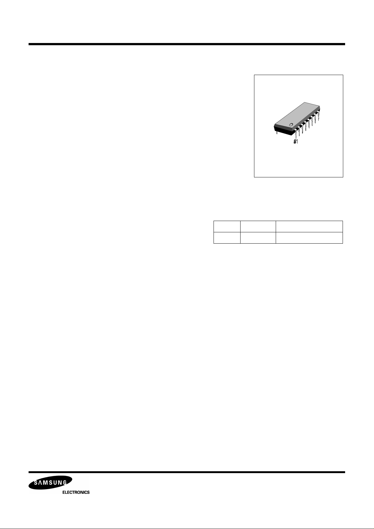
16-DIP-300
Device Package Operating Temperature
KS2508 16-DIP-300 0°C ~ 70°C
• Programmable vertical and horizontal positioning
• Character color selection up to 16 different colors
• Programmable background color (Up to 16 colors)
• Character blinking, bordering and shadowing
• Color blinking
• Character scrolling
• Fade-in and fade-out
• Box drawing
• Character sizing up to four times
• 96 MHz pixel frequency from on-chip PLL
• IIC Protocol Data Transmission (Slave Address : BAH)
1

Preliminary
KS2508 OSD PROCESSOR FOR MONITOR
BLOCK DIAGRAM
SDA
SCL
HFLB
VFLB
ROM
Addr
9
Display
Control
Timing
Controller
Single Color ROM
(256 x 18x12)
Font
12
Data
Output
Stage
H/V/CLK
Control
15
14
13
12
11
INT
R_OU T
G_OUT
B_OUT
FBLK
Control
Data
Control
Control
Control
Control
RAM
Data
16
Frame
Row
Frame
Row
RAM
(480 x 16)
Font
Control
Display
Controller
H/V/CLK
Control
7
8
Data
Receiver
16
Control Register
CLK
6
OSD
_PLL
9
H-Pulse
V-Pulse
2 3 5 1 4 10 16
VCO_IN
VREF1
VREF
VSS_A
VDD_A
VSS_D
VDD_D
Figure 1. Functional Block Diagram
2
Preliminary
KS2508 OSD PROCESSOR FOR MONITOR
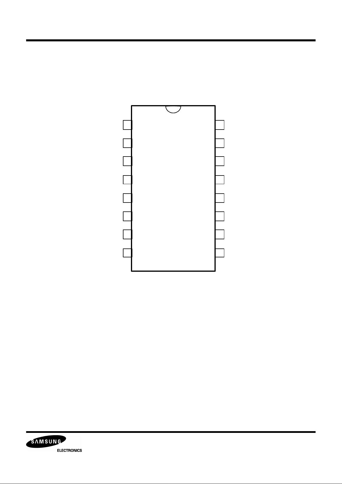
PIN CONFIGURATIONS
VSS-A 1
VCO-IN
VREF1
VDD- A 4
VREF 5
HFLB
SDA
SCL 8
VDD _D16
2
3
15
14
INT
R_OUT
G_OUT13
KS2508
B_OUT12
6
7
11
10
FBLK
VSS_D
VFLB9
Figure 2. Pin Configurations
3
Preliminary
KS2508 OSD PROCESSOR FOR MONITOR
PIN DESCRIPTIONS
Table 1. Pin Descriptions
Pin No. Signal Active I/O Description
1 VSS_A - - Ground (Analog Part)
2 VCO_IN - Input This voltage is generated at the external loop filter and
goes into the input stage of the VCO.
3 VREF1 - Input 1.26 V DC Voltage from the Bandgap Reference.
Connected to ground through a resistor to make internal
reference current (Typical 36 KΩ for 27µA)
4 VDD_A - - +5 V Supply Voltage for Analog Part
5 VREF - Input Bandgap Reference Voltage (Typical 1.26 V)
6 HFLB Low Input Horizontal Flyback Signal
7 SDA - In/Out
8 SCL - In/Out
9 VFLB Low Input Vertical Flyback Signal
10 VSS_D - - Ground for Digital Part
11 FBLK - Output Fast Blank Signal
12 B_OUT - Output Video Signal Output (B)
13 G_OUT - Output Video Signal Output (G)
14 R_OUT - Output Video Signal Output (R)
15 INT - Output Intensity Signal Output
16 VDD_D - - +5 V SUpply Voltage for Dogital Part
Serial Data (I2C)
Serial Clock (I2C)
4

Preliminary
KS2508 OSD PROCESSOR FOR MONITOR
ABSOLUTE MAXIMUM RATINGS
Parameters Symbol Value Unit
Min. Typ. Max.
Maximum Supply Voltage VDD - - 7.0 V
Input Voltage V
Operating Temperature Range T
Storage Temperature Range T
Power Dissipation P
I
OPR
STG
D
- - 7.0 V
-20 - 70
-40 125
- - 1200 mW
NOTE: PKG Thermal Resistance : 64.2 °C/W
ELECTRICAL CHARACTERISTICS
DC Electrical Characteristics
(Ta = 25 °C, VDD = 5 V)
Table 2. DC Electrical Characteristics
Parameters (Conditions) Symbol Min. Typ. Max. Unit
Supply Voltage VDD 4.75 5.00 5.25 V
Supply Current
(No load on any output)
Input Voltage
I
V
V
DD
- - 25 mA
IH
IL
0.8VDD
-
-
-
- V
VSS + 0.4 V
°C
°C
Output Voltage
(lout = 1mA)
Input Leakage Current I
VCO Input Voltage V
V
V
VCO
OH
OL
IL
0.8VDD
- -
-10
-
- V
VSS + 0.4 V
-
10 µA
2.5 V
5
Preliminary
KS2508 OSD PROCESSOR FOR MONITOR
OPERATION TIMINGS
Table 3. Operation Timings
Parameters (Conditions) Symbol Min. Typ. Max. Unit
Output Signal - R/G/B_OUT, INT, FBLK (Ta = 25°C VDDA = VDD = 5 V , CLOAD = 30pF)
Rise Time t
Fall Time t
Input Signal - HFLB, VFLB
Horizontal Flyback Signal Frequency f
Vertical Flyback Signal Frequency f
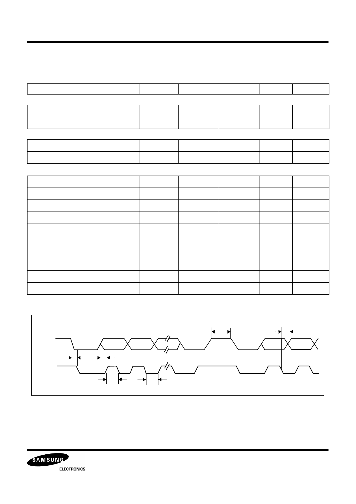
I2C Interface - SDA, SCL (Refer to Figure 3)
SCL Clock Frequency f
Hold Time for start condition t
Set Up Time for stop condition t
Low Duration of clock t
High Duration of clock t
Hold Time for data t
Set Up Time for data t
Time between 2 access t
Fall Time of SDA t
R
F
HFLB
VFLB
SCL
hs
sus
low
high
hd
sud
ss
fSDA
- - 6 nsec
- - 6 nsec
- - 120 kHz
- - 200 Hz
- - 300 kHz
500 - - ns
500 - - ns
400 - - ns
400 - - ns
0 - - ns
500 - - ns
500 - - ns
- - 20 ns
Rise Time of both SCL and SDA t
SDA
SCL
t
hs
t
t
high
sud
t
Figure 3. I2C Bus Timing Diagram
low
rSDA
- - - ns
t
t
ss
hd
6
Preliminary
KS2508 OSD PROCESSOR FOR MONITOR
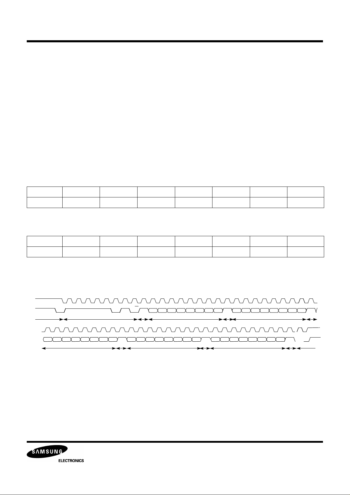
FUNCTIONAL DESCRIPTIONS
Data Transmission to the KS2508
According to the I2C protocol, the KS2508 receives the data from a micro controller. The SDA line and the SCL line
are shown in Figure 4. As shown in Figure 4, after the starting pulse, the slave address with R/W* bit and an
acknowledge are transmitted in sequence, an internal register address of the KS2508 is followed. The first 8-bit
byte is the upper 8bits of the register address. The lower 8bits of the register address are followed after the second
acknowledge. There is a data transmission format and are two address bit patterns in the KS2508 as following.
The slave address of the KS2508 is BAH(in hexadecimal).
Data Transmission Format
Row Address -> Column Address -> Data Byte N -> Data Byte N+1 -> Data Byte N+2 -> ....
Address Bit Pattern for Display Registers Data
(a) Row Address Bit Pattern R3 - R0: Valid Data for Row Address
A15 A14 A13 A12 A11 A10 A9 A8
X X X X R3 R2 R1 R0
(b) Column Address Bit Pattern C4 - C0: Valid Data for Column Address
A7 A6 A5 A4 A3 A2 A1 A0
X X X C4 C3 C2 C1 C0
After addressing, data bytes are followed as the above data transmission format. The Figure 4 describes the data
transmission with the I2C bus protocol.
SCL
SDA
START IIC SLAVE ADDRESS ACK MSB ADDRESS ACK LSB ADDRESS ACK
SCL
D1 D0D2D3D4D5D6D7
DATA BYTE N(MSB DATA)
R/W
D1 D0D2D3D4D5D6D7SDA D1 D0D2D3D4D5D6D7
ACK DATA BYTE N(MSB DATA) ACK STOPACK DATA BYTE N(LSB DATA)
A5 A4 A3 A2 A1 A0A6A7A9 A8A10A11A12A13A14A15
...
...
Figure 4. SDA line and SCL line (Write Operation)
7
 Loading...