

Page 1

Chapter 3
IC Description &
3-1 MC68EC000...............................................3-2
3-2 STC 9604 ...................................................3-8
3-3 STL 7053 (TMC).......................................3-15
3-4 STI 9511 (QDMC).....................................3-17
3-5 TP 3404 (QDASL).....................................3-21
3-6 SBS 9401 .................................................3-24
3-7 CODEC (TP3057).....................................3-26
3-8 STL 7065..................................................3-28
3-9 TIMING CHART........................................3-29
Page 2
Chapter 3. IC Description & Timing
3-1 MC68EC000
3-1-1 General
The MC68EC000 of Motolora is used as processor for DCS COMPACT II(PLUS)main system.
MC68E000 is an economic version of MC68EC000. The MC68EC000 has supported by a
statically selectabe 8-bit or 16-bit data bus. This architecture provides a fast and efficient
processing device that can satisfy the requirements of sophisticated applications based on
high-level language.
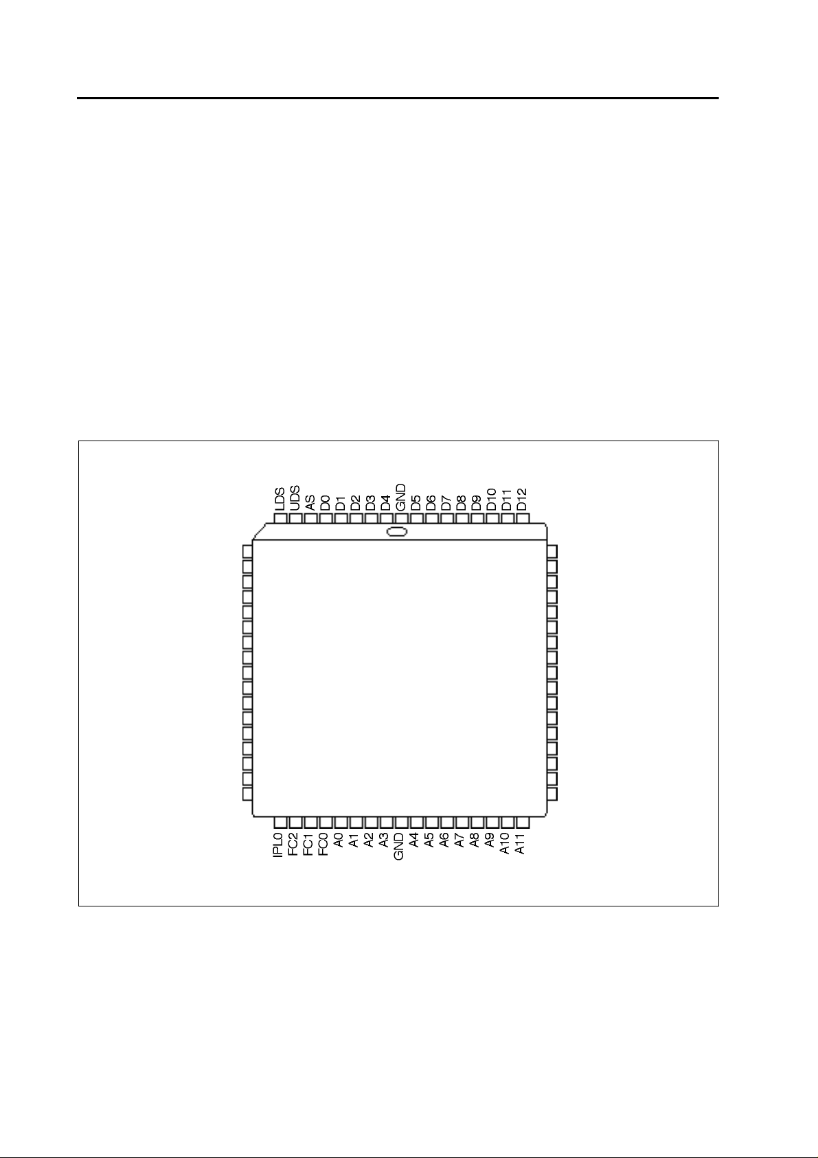
3-1-2 Pin Map
R/W
DTACK
BG
BR
Vcc
Vcc
CLK
GND
GND
MODE
HALT
RESET
NC
AVEC
BERR
IPL2
IPL1
9 68 61
10
MC68EC000
26
60
D13
D14
D15
GND
A23
A22
A21
Vcc
A20
A19
A18
A17
A16
A15
A14
A13
A12
44
4327
3-2
Page 3

Chapter 3. IC Description & Timing
3-1-3 Circuit Description
Address Bus (A0~A23)
This 24bit, unidirectional, three-state bus is capable of addressing 16Mbytes of data. It provides
the address for bus operation during all cycles except interrupt cycles. During interrupt cycles
A3, A2, and A1 reflect the level of the interrupt being serviced while A23~A4 and A0 are set to
a logic high.
Data Bus (D0~D15)
This 16bit bidirectional, three-state bus is the general-purpose data path. If the controller is
operating in the 16bit mode, the data bus transfers and accepts data in either word or byte
length. If the controller is operating in the 8 bit mode, the controller drives the entire bus during
writes, but only the lower eight bits (D7~D0) contain valid data. In the 8 bit mode, the controller
ignores the data on D15~D8 during read cycles. During and interrupt acknowledge cycle the
external device supplies the vector number on D7~D0.
Aynchronous Bus control
Aynchronous data transfers are handled using the following control signals : address strobe,
read/write, upper and lower data strobes, and data transfer acknowledge.
Address Strobe(AS)
This signal indicates a valid address on the address bus.
Read/Write (R/W)
This signal defines the data bus transfer as a read or write cycle. R/W also works in conjunction
with the data strobes as explained in the following paragraph.
3-3
Page 4
Chapter 3. IC Description & Timing
Upper and Lower Data Strobe (UDS, LDS)
These signals control the flow of data on the data bus as listed in Table. When R/W is high, the
controller reads from the data bus as indicated. When R/W is Low, the controller writes to the
data bus as shown. During operation in the 8 bit mode, the UDS is always forced high and LDS
indicates valid data.
Data Strobe Control of Data Bus for 16 Bit Mode
UDS
1
0
1
0
0
1
0
These condition are result of current implementation and may not appear on future device.
LDS
1
0
0
1
0
0
1
R/W
–
1
1
1
0
0
0
D15 ~ D8
No Valid Data
Valid Data Bits 15 ~ 8
No Valid Data
Valid Data Bits 15 ~ 8
Valid Data Bits 15 ~ 8
Valid Data Bits 7 ~ 0
Valid Data Bits 15 ~ 8
D7 ~ D0
No Valid Data
Valid Data Bits 7 ~ 0
Valid Data Bits 7 ~ 0
No Valid Data
Valid Data Bits 7 ~ 0
Valid Data Bits 7 ~ 0
Valid Data Bits 15 ~ 8
Data Transfer Acknowledge(DTACK)
This input indicates that the data transfer is complete. When the controller recognizes DTACK
during a read cycle, data is latched and the bus cycle is terminated. When DTACK is
recognized during a write cycle the bus cycle is terminated.
Bus Arbitration Control
Bus request and bus grant form a bus arbitration circuit to determine which device will be the
bus master.
Bus Request(BR)
This input indicates that an external device requires bus mastership.
3-4
Page 5

Chapter 3. IC Description & Timing
Bus Grant(BG)
This output indicates to all other potential bus master devices that the controller will release bus
control at the end of the current bus cycle.
Interrupt Control
The interrupt priority level signals and autovector signal are used in servicing external interrupts.
Interrupt Priority Level (IPL2, IPL1, IPL0)
These inputs indicate the encoded priority level of the device requesting an interrupt. Level 7 is
the highest priority; whereas, level 0 indicates that no interrupts are requested. Level 7 cannot
be masked. The least significant bit is given in IPLO, and the most significant bit is contained in
IPL2. These lines must remain stable untile the controller signals interrupt acknowledge
(FC2~FC0 are all High) to ensure that the interrupt is recognized.
Autovector(AVEC)
This input indicates that the controller should use automatic vectoring for an interrupt during an
interrupt acknowledge cycle.
NOTE : AVEC should be asserted only during an interrupt acknowledge cycle, or erratic
controller operation could occur.
3-5
Page 6

Chapter 3. IC Description & Timing
System Control
The four system control inputs are used to reset or halt the controller, to indicate that the
controller state bus errors have occurred, and to switch from 8 bit to 16 bit operating mode.
Reset (RESET)
The bidirectional signal resets (starts a system initialization sequence)the MC68EC000 in
response to an external RESET signal. An internally generated reset (result of a RESET
instruction) causes all external devices to be reset, and the internal state of the controller is not
affected A total system reset (controller and external devices) is the result of external HALT and
RESET signals applied simultaneously.
Halt(HALT)
When this bidirectional line is driven by an external device, it causes the controller to stop at the
completion of the current bus cycle. When the controller has been halted using this input, all
control signals are inactive, and all three-state lines are put in their high-inpedance state.
When the controller stop executing instructions, such as in a double bus fault condition, the
HALT line is driven by the controller to indicate to external devices that the controller has
stopped.
Bus Error (BERR)
This input informs the controller that there is a problem with the bus cycle currently being
executed.
Problems may be a result of:
°‹Nonresponding devices,
°‹Interrupt vector number acquisition failure,
°‹Illegal access request as determined by a memory management unit, or
°‹Other application-dependent errors.
The bus error signal interacts with the halt signal to determine if the current bus cycle should be
reexecuted or if exception processing should be performed.
3-6
Page 7
Chapter 3. IC Description & Timing
Mode (MODE)
The MODE input selects between the 8 bit and 16 bit operating modes. If this input is grounded
at reset, the controller will come out of reset in the 8 bit mode. If this input is tied high or floating
at reset, the controller will come out of reset in the 16 bit mode. This input should be changed
only at reset and must be stable two clocks after RESET in negated. Changing this input during
normal operation may produce unpredictable results.
Processor Status (FC2, FC1, FC0)
These function code outputs indicate the state (user or supervisor) and the cycle type currently
being executed. The information indicated by the function code outputs is valid whenever
address strobe (AS) is active.
Function Code Outputs
Function Code Output
FC2
0
0
0
0
1
1
1
1
FC1
0
0
1
1
0
0
1
1
FC0
0
1
0
1
0
1
0
1
(Undefined, Reserved)
User Data
User Program
(Undefined, Reserved)
(Undefined, Reserved)
Supervisor Data
Supervisor Program
Interrupt Acknowledge
Cycle Time
Clock (CLK)
The clock input is a TTL-compatible signal that is internally buffered for development of the
internal clock needed by the controller, The clock input should not be gated off at any time. and
the clock signal must conform of minimum and maximum pulse-width times. The clock is a
constant-frequency square wave with no stretching or shaping techniques required.
3-7
Page 8
Chapter 3. IC Description & Timing
3-2 STC-9604
3-2-1 GENERAL
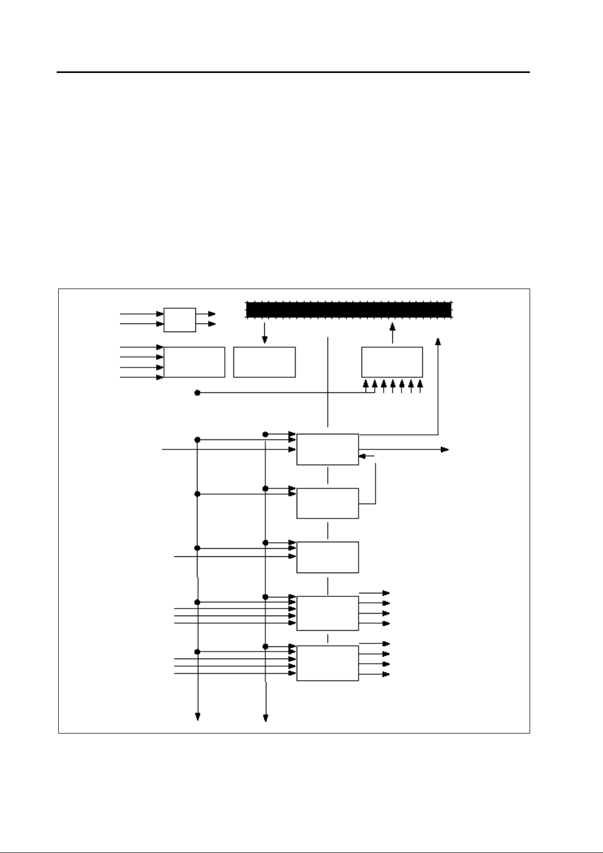
STL-9604 is ASIC which performs various functions. It controls main system. Included are
DPLL, Clock Generation, Time Switch, Digital Conference, Multi-Tone/DTMF Detector, QDASL
Control, TMC control.
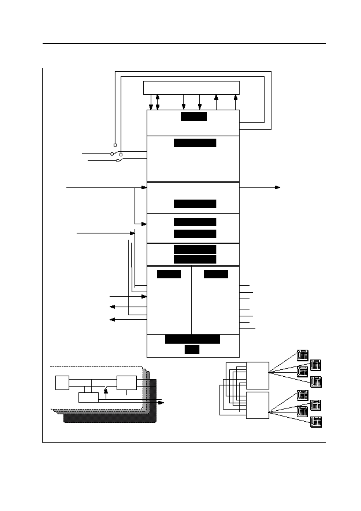
3-2-2 Block Diagram
IC8K
IACT
C10M
C4M
FOIB
T1DET
IHWR[7:0]
IDSPIN
IHOS[7:0]
IRING[7:0]
IMETGND[7:0]
DPLL
Clocks
Generation
OFOIB
OC4M
ADDRESS
Address
Decode
CPU Interface
DATA IPL
TSW &
CONFERENC
E
DTMF/TONE
Generation
DTMF/TONE
Detection
8TMC
DTACK
INT
Control
OHWX[7:0]
OPSX[7:0]
ODP[7:0]
OMUTE[7:0]
ORING[7:0]
IRXD
ICI
IDINT[1:0]
3-8
8DMC
OTXD
OCD
OCS[1:0]
OCCLK
Page 9
CPU
Chapter 3. IC Description & Timing
FOIB from T1
ADR
C16M
C4M
FOIB
T1DET
IHWR[7:0]
IDSPIN
IHOS[7:0]
IRING[7:0]
IMETGND[7:0]
OFSX[7:0]
ODP[7:0]
OMUTE[7:0]
DATA DS AS IPL
DPLL
IC8K
IACT
Clock Gen.
TSW/CONF
TSW/CONF
DETECTION
DTMF/TONE
Generation
TMC DMC
DTACK
OPOIB
OC4M
OHWX[7:0]
IRXD
ICI
IDINT[1:0]
OTXD
OCO
OCS[1:0]
OCCLK
8 Trunks
C.D.
Generation Purpose
IRXD
T
PING
F
Detect
DC
Bypass
SIO
OTXD
OINTSIO
QDASL
QDASL
3-9
Page 10
Chapter 3. IC Description & Timing
CPU
NEW
ENG
ODSPEN1B
ODSPEN1B
CPU
CPU Borad
NEW
ENG
STL
7065
STL
7065
ODSPEN1B
ODSPEN1B
IDSPCEB
IDSPCEB
AA B0rad
STL
7065
STL
7065
IDSPCEB
IDSPCEB
3-10
Page 11

3-2-3 Pin Map
Chapter 3. IC Description & Timing
105
156
OFSK
ORAFSX
OO10M
IT1DET
OO405M
IALAWUB
OC8M
GND4
IC4MI
VDD29
IPC12M
GND10
IPC8K
VDD22
OPC1544M
OPC4M
OPFOIB
OFOIBEXT
VDD25
IC16M
GND15
ORAMEN1B
ORAMEN2B
ORAMEN3B
ORAMEN4B
VDD28
IRNG7
IRNG6
IRNG5
IRNG4
IRNG3
IRNG2
IRNG1
IRNG0
GND32
IHOS7
IHOS6
IHOS5
IHOS4
IHOS3
IHOS2
IHOS1
IHOS0
VDD20
IMETER7
IMETER6
IMETER5
IMETER4
IMETER3
IMETER2
IMETER1
IMETER0
104
STC-9604
53
GND5
IFC1
IFC2
OAVECB
VDD19
OC1K
ODTACK
ISRWB
ISDSB
ISASB
OINTIDB
BND11
IEXT3B
GND11
IEXT38
OEXDENB
GND12
BSD0
BSD1
BSD2
BSD3
BSD4
BSD5
BSD6
BSD7
VDD18
OPCMCIAB
GND2
ISA0
ISA1
ISA2
ISA3
ISA4
ISA5
ISA7
ISA8
ISA9
GND16
ISA13
ISA14
ISA15
ISA16
ISA17
ISA18
ISA19
VDD31
OROMEN2B
OROMEN1B
OINTUARTB
OSTXD
ISRXD
ICODEEN
52
1
157
208
3-11
Page 12

Chapter 3. IC Description & Timing
3-2-4 Feature Description
Time switch
°‹Performs switching on 8 highways 256channels.
°‹Switching configuration is achieved by writing channel address into the switching address
field (low byte) in control memory.
°‹It is possible to control memory each channel’s high impedance state for 8 output highway.
°‹8 step gain control (2.8 to – 6dB)
Digital Conference
°‹Provides 5 way 6 group conference.
°‹Up to 6 of 256 channels can be assigned to conference member.
°‹Conference member assignment is achieved by writing the group ID to the relevant
conference group fields of the selected channel contrl memory.
°‹It is possible to control each channel’s noise suppression.
°‹8 step gain control (2.8 to - 6dB) for added speech.
°‹It is possible to show that overflow occur during conference.
°‹It is possible to mask specific conference group member channel output.
QDASL CONTROL
°‹Control 2 Quad-DASL Chip (TP3404) made by National Semiconductor.
°‹It is possible to TX/RX data with URAT for D chnnel.
°‹Programmable UART speeds (2K/4K/8K/16Kbps)
°‹B channel can do bypass matching.
°‹Microwried serial controll (16bit) matching.
TMC CONTROL
°‹Dial Pulse Generator
°‹Time Slot Generator
°‹Input detector & Output port control
°‹Each 8 ports
3-12
Page 13

Chapter 3. IC Description & Timing
COMMON
°‹Support A-law/µ-law PCM
°‹Speech memory read
°‹Control memory read/write
°‹It is possible to control Tone data output with CMH(contrl memory high byte) D7 bit.
°‹Conference Control Register Read/Write
°‹Overflow Status Register Read
°‹It is possible to control High impedance state of highway output pin.
°‹Signalling Memory Read Enable
°‹Control Memory Read Enable
S/W Control Procedure
Power on Reset
All output highway are forced high impedance status by setting the highway output control
register.
Control Memory Initialize
It is necessary to be initialized by CPU, because the control memory is not initialized with Reset
feature. Especially, high byte of conference group must be initialized to be no conference(111or
110).
CML(Address 40200H~402FFH) : Channel address write
CML(Address 40300H~403FFF) : 70H write
Highway Output Control Register Clear
Output highway is enabled by writing 00H
3-13
Page 14

Chapter 3. IC Description & Timing
Control Memory Write
°‹Write each channel’s address into the control memory low byte of two channels that is
connected. For example, if you want to connect 0 highway 3 channel address 03H and 3
highway 7 channel address 67H together, write 67H into 44003H address and 03H into
44067H address to connect both of them.
°‹Write a proper value the control memory high byte according to the connected cahnnel
attributes.
Conference Configuration
°‹Assign the noise reduction mode by setting the conference channel mask bit of the relevant
group conference control register to ON.
°‹Write its own channel address to the control memory low byte of conference member.
°‹Write conference group/gain control mode into the control memory high byte.
°‹After 2 frames, overflow can be checked during conference. Adjust the gain control mode of
control memory high byte if necessary.
Overflow status check
°‹It is possible to check overlfow during conference and adjust gain control mode of control
memory high byte, if neccesary, with reading 42006H.
3-14
Page 15

Chapter 3. IC Description & Timing
3-3 STL 7053 (TMC)
3-3-1 General
Controller IC STL7053 (TMC : Trunk Module Controller) consists of Dial pulse generator,
Channel assign generator, Relay control, and the other logics.
The dial pulse can be selected between 50mSec and 100mSec cycles, and the channel assign
generator section supports up to 5 ports and each channel assign signal has timing which
supports CODEC (specially, TP3057).
3-3-2 Pin Map
TSXB
TSEXT
EXTACT01
HWTXIN
HWRXOUT
HWTXOUT
HWRXIN
A4
VDO
A5
A6
A7
FS
CLKX
VSS
45 44 43 42 41 40 39 38 37 36 35 34 33 32 31
46
47
48
49
50
51
52
53
54
55
56
57
58
59
60
1 2 3 4 5 6 7 8 9 10 11 12 13 14 15
S T L 7 0 5 3
30
29
28
27
26
25
24
23
22
21
20
19
18
17
16
VSS
HOS1
RING1
MUTEGND1
DP1
METGND1
TS0
HOSO
VDD
RING0
MUTEGND0
DP0
METGND0
MODE
ALAWBMU
3-15
Page 16

Chapter 3. IC Description & Timing
3-3-3 Function Module Map
Mode
0
1
0
1
0
1
0
Address
A12 A7 A6 A5 A5
0 0 0 0 0
0 0 0 0 1
0 0 0 1 0
0 0 0 1 1
0 0 1 0 0
0 0 1 0 1
0 0 1 1 0
0 0 1 1 1
1 0 0 0 0
1 0 0 0 1
1 0 0 1 0
1 0 0 1 1
1 0 1 0 0
1 0 1 0 1
1 0 1 1 0
1 0 1 1 1
0 1 0 0 0
0 1 0 0 1
0 1 0 1 0
0 1 0 1 1
0 1 1 0 0
0 1 1 0 1
0 1 1 1 0
0 1 1 1 1
1 1 0 0 0
READ DATA
D7-D4 D3 D2 D1 D0
R
M
X
X
0 0 0 0 1
E
T
E
X
R
or
G
N
D
(card ID)
X
All 0°Øs
X
All 0°Øs
H
I
O
N
S
G
Dial pulse read
Dial pulse read
X
X
E
N
A
B
Contor1
L
E
EXTAT01
D7
EXTAT01
D7
Enable
Write Data
M
L
E
T
E
R
or
G
N
D
L
O
O
O
O
P
P
#
#
2
1
Gain
100msec/50msec
Dial pulse Write
100msec/50msec
Dial pulse Write
X
Ext Time slot
Dial
Number
(1-A)
Time Slot
Assign
D0
D0
1
1 1 1 0 0
X
X
Ext Time slot
3-16
Page 17

Chapter 3. IC Description & Timing
3-4 STI-9511 (QDMC)
3-4-1 General
DLI module control STI-9511 performs signalling control, channel assigning, and QDASL
(TP3404) control between the main system and digital telephone.
3-4-2 Pin Map
Test pin #7
Test pin #8
Test pin #9
Test pin #10
Vdd
DCTEST1
MODE2
Test pin # 11
Addr12
MODE1
Test pin #12
Addr7
MODE0
GND
PORB
46 31
STI-9511
(Quad DASL Controller)
60-QFP-1414A
1
16
GND
Test pin #2
INTB2
INTB1
INTB0
Vdd
Test pin#1
FS
BCLK
GND
C4M
GND
DLIENB
Test pin#0
RWB
3-17
Page 18

Chapter 3. IC Description & Timing
3-4-3 Funtional Description
Chip
Expansion
The chip expansion is determined by input pin. Up to 4 chip can be used for one board. Input
pin & ID value is as follows.
Mode#1
Pin#55
0
0
1
1
D7
S/W
Reset
Add#12
Pin#54
0
1
0
1
Mode#0
Pin#58
0
0
1
1
The rests of Decodings
Add#7
Pin#57
0
1
0
1
Card & Chip ID value
Chip#0:Card ID(07£‹h)
Chip ID(01£‹h)
Chip#1:Card ID(07£‹h)
Chip ID(02£‹h)
Chip#2:Card ID(07£‹h)
Chip ID(03£‹h)
Chip#3:Card ID(07£‹h)
Chip ID(04£‹h)
Card ID or Chip ID value can°Øt
readable(00£‹h)
D6 D5 D4 D3 D2 D1 D0
Speed
Speed
MASK
MASK
X X
sel #1
sel #0
Bit allocation table of Mode setting Register
Tx
Rx
MASK
DASL
– D7 Bit : software Reset
– D6, D5 Bit : UART speed
Speed (D6)
0
0
1
1
Speed (D5)
0
1
0
1
– D4, D3 Bit : Don’t care
– D2, D1, D0 Bit : Interrupt Masking Bit
Comments
2Kbps(Speed of D-ch Transceiver)
4Kbps(Speed of D-ch Transceiver)
8Kbps(Speed of D-ch Transceiver)
16Kbps(Speed of D-ch Transceiver)
3-18
Page 19

Chapter 3. IC Description & Timing
UART
UART performs data signalling. It transmits the values written into a register by the processor,
in accordance with the transmission speed as the serial data stream of TxD. It converts RxD
(serial input data stream) to parallel and stores into a data buffer to be read by the processor.
The main purpose is to be signalling by forming the D-channel data stream with the interface
with DASL chip.
D7 D6 D5 D4 D3 D2 D1 D0
X
sel #1
Speed
Speed
sel #0
Parity
Error
UART Status Register
Tx
Full
Tx
Empty
Rx
Full
Rx
Empty
When status change occurs, the register is active high. The bit of assigned order is as follows.
D4 : Parity Error (High if error occurs after checking even parity)
D3 : Tx full (High if 3 byte exist in Tx buffer)
D2 : Tx Empty (High if the data to be transmitted does not exist in Tx buffer).
D1 : Rx full (High if 3 byte exist in Rx buffer)
D0 : Rx Empty (If the data received does not exist in Rx buffer)
Interrupt structure
– INTRD0 (Pin#26 : UART Rx Interrupt Read)
D7 D6 D5 D4 D3 D2 D1 D0
INT Rx
Port #7
INT Rx
Port #6
INT Rx
Port #5
INT Rx
Port #4
INT Rx
Port #3
INT Rx
Port #2
INT Rx
Port #1
INT Rx
Port #0
– INTRD1 (Pin#27 : UART Tx Interrupt Read)
D7 D6 D5 D4 D3 D2 D1 D0
INT Tx
Port #7
INT Tx
Port #6
INT Tx
Port #5
INT Tx
Port #4
INT Tx
Port #3
INT Tx
Port #2
INT Tx
Port #1
– INTRD2 (Pin#28 : External Interrupt Read)
Occur interrupt with receiving signal from TP3404.
3-19
INT Tx
Port #0
Page 20

Chapter 3. IC Description & Timing
B-Channel Interface
STI-9511 concerned with B-channel controls Tx/Rx time slot allocation through Microwired
interface.
Microwired Interface
To control 2 TP3404, the output of STI-9511 (CO(Pin#38), CCLK(Pin#41), CSB0(Pin#31),
CSB1(Pin$43)) is connected to input of TP3404’s Microwired Interface (CI(Pin#21),
CCLK(Pin#19), CSB(Pin#18, 1st TP3404), CSB(Pin#18, 2nd TP3404)), and input of STI-9511
(CI(Pin#40) is connected to CO (Pin#20) of TP3404. As this method, Microwired Interface
(serial interface) can realize. Microwired interface of TP-3404 is changed to 16bit from 8bit.
There are chip enable register, address register, data register to controls 2 TP3404 with 1
STI-9511.
D1 Bit
0
0
1
D0 Bit
0
1
0
Comment
Assign to Sub-time slot this chip
1st TP3404 Microwired Enable(Active ° ∞Low°±)
2nd TP3404 Microwired Enable(Active ° ∞Low°±)
D-channel Interface
Two signal is needed to Tx/Rx D-channel’s data to TP3404 with Serial Data Stream.
RxD (Pin#34) transfers data of D-channel from TP3404 to Processor, and TxD (Pin#36) is vice
versa. UART format for D-channel interface is as follows.
Start Bit Transmission Data
Start Bit(1Bit : Low)+Transmission Data(8Bit)+Praity Bit(Even)+Stop Bit(1Bit :High)
Parity Bit Stop Bit
3-20
Page 21

Chapter 3. IC Description & Timing
3-5 TP3404 (QDASL)
3-5-1 General Description
The TP3404 is a combination 4-line transceiver for voice and data transmission on twisted pair
subscriber loops, typically in line card interface. It is companion device to the TP3401/2/3 DASL
single-channel transceivers. In addition to 4 independent transceivers, a time-slot assignment
circuit is included to support interfacing to the system backplane. Each QDASL line operates as
an ISDN “U” Interface for short loop applications, typically in a PBX evnironment, providing
transmission for 2B channels and 1D channel. Full-deplex transmission at 144kbps is achieved
on single twisted wire pairs using a burst-mode technic (Time Compression multiplexed).
Alternate mark Inversion (AMI) line coding is used to ensure low error rates in the presence of
noise with lower EMI radiation than other codes such as Biphase manchester).
3-5-2 Features
– Quad 2B plus D channel interface for PBX “U” interface.
– 144kbps full-duplex on 1 twisted pair using Burst Mode Transmmission Technique
– Loop range up to 6 kft (#24AWG)
– Alternate Mark Inversion coding with transmit Pulse Shaping DAC, Smoothing filter, and
scrmbler for low EMI radiation
– Adaptive line equalizer
– On-chip timing recovery, no external components
– Programmable Time-Slot Assignment TDM interface for B channel
– Separate interface for D channel, with Programmable Sub-Slot Assignment
– 4.096MHz master clock
– MICROWIRE compatible serial control interface
– 5V operation
– 28-pin PLC package
3-21
Page 22

Chapter 3. IC Description & Timing
3-5-3 Block Diagram
VCCD
VCCA MCLK
BCLK
FS
BO
TSB
DO
CCLK
CS
CO
INT
BI
DI
CI
TIME-SLOT
ASSIGNER
CONTROL
STATUS
REGISTER
3-5-4 Pin Description
&
Li0
NC
DO
MCLK
BCLK
FS
SCRAMBLER
FRAMER
AMI CODER
FRAME SYNC
DESCRAMBLER
LINE #1
LINE #2
LINE #3
TX DAC
RECEIVER
LINE SIGNAL
DETECT
Lo0
Li0
Lo1
Li1
Lo2
Li2
Lo3
Li3
GNDD GNDA
Lo3
Li3
DI
NC
NC
Ci
Co
CCLK
3-22
Page 23

Chapter 3. IC Description & Timing
PIN NO
1
15
28
16
11
9
10
12
13
14
7
8
19
21
17
20
18
4, 3,
26, 25
5, 2,
27, 24
PIN NAME DESCRIPTION
GNDA
GNDD
VDDA
VDDD
FS
MCLK
BCLK
BI
BO
/TSB
DI
DO
CCLK
CI
/INT
CO
/CS
Lo0, Lo1,
Lo2, Lo3
Li0, Li1,
Li2, Li3
Analog Ground or 0V. All analog signals are referenced to this pin.
Digital Ground 0V. It must connect to GNDA with a shortest possible trace. This can be
done directly underneath the part.
Possible power supply input to QDASL analog section.It must be 5V±5%.
Positive power supply input to QDASL digital section. It must be 5V±5%, and connect to
VDDA with the shortest possible trace. This can be done directly undernearth the part.
Frames Sync input: this signal is the 8KHz clock which defines the start of the transmit
and receive frames at the digital interface.
This pin is the 4.096MHz master clock input, which requires a CMOS logic level clock
from a stable source. MCLK must be synchronous with BCLK.
Bit clock logic input, which determin the data shift rate for B and D channel data at the
BI, BO, DI and DO pins. BCLK may be any multiple of 8KHz from 256KHz to 4.096KHz,
but must be synchronous with MCLK.
Time-division multiplexed input for B1 and B2 channel data to be transmitted to the 4
lines. Data on this pin is shifted in on the failling edge of BCLK into the B1 and B2
channel during selected transmit time-slots. Time-division multiplexed receive data
output bus. B1 and B2 channel data from all 4 lines is shi.
Time-division multiplexed receive data output bus. B1 and B2 channel data from all 4
lines is shifted out on the rising edge of BCLK on this pin during the assigned receive
time-slots. At all other times this output is TRI-STATE (high impedance)
This pin is an open-drain output which is normally high impedance but pulls low during
any active B channel receive time slots at the BO pin.
Time-division multiplexed input for D channel data to be transmitted to the 4 lines. Data
on this pin is shifted in on the failling edge of BCLK into the D channel during the
selected receive sub-time-slot.
Time-division multiplexed output for D channel data received from the 4 lines. Data on
this pin is shifted out on the rising edge of BCLK during the selected receive sub-timeslot.
Microwire Control Clock input. This clock shifts serial control information into CI and out
from CO when the /CS input is low, depending on the current insruction. CCLK may be
asynchronous with the other system clocks.
Control data input. Serial control information is shifted into the QDASL on this pin on the
failing edges of CCLK when /cs low.
Interrupt request Output, a latched output signal which is normally high impedance and
does low to indicate a change of status of any of the 4 loop transmission systems. This
latch is cleared when the Status Register is read by the microprocessor. Bipolar
Violation does not effect this output.
Control data output. Serial control/status information is shifted out from the QDASL on
this pin on the failling edges of CCLK when /CS low.
Chip select input. When this pin is pulled low, the Microwire interface is enabled to allow
control information to be written in to and out from the device via the CI and CO pins.
When high, this inhibits the microwire.
Line drive transmit outputs for the 4 transmission channels, Each output is an amplifier
intended to drive a transformer.
Line receive amplifier inputs for the 4 transmission channels. Each LI pin is a self-biased
impedance input which should be connected to the transformer via the recommended
line interface circuit.
3-23
Page 24
Chapter 3. IC Description & Timing
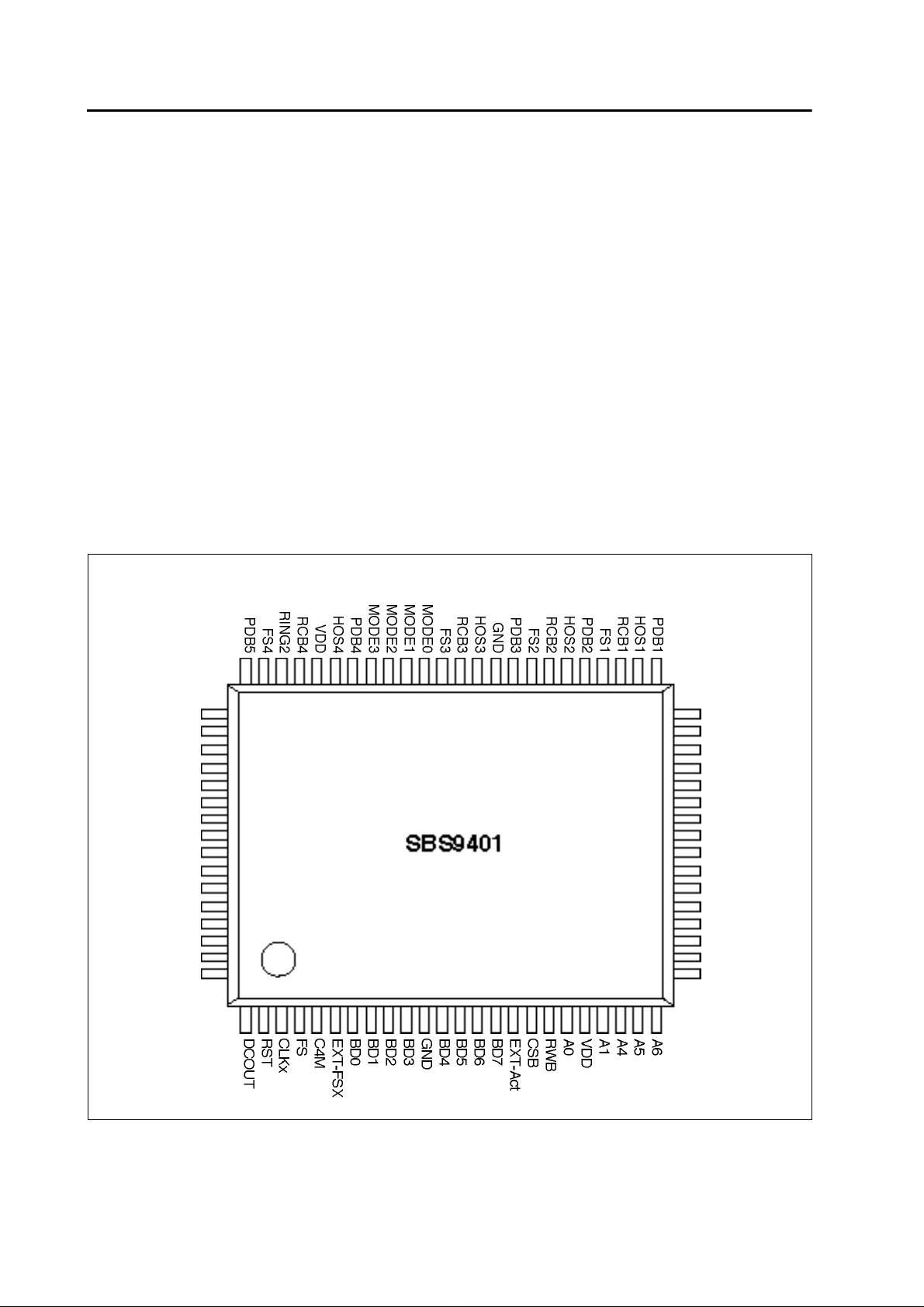
3-6 SBS 9401
3-5-1 Features
°‹8 ports TSAC (Time Slot Assignment Control)
°‹4 port UART (Universal Asynchronous Receiver & Transmitter)
°‹Signalling with 4 ports of digital telephone by controlling 4 ports RASL (Reduced Digital
Adaptor for Subscriber Loops) through microchannel control.
°‹4 ports dial pulse generating.
°‹Designed to be used for 4 trunk type, 204 DLI type, 8 SLI type or 204 SLI type.
°‹
For DCS COMPACT II (PULS) system, 8 SLI type is used. TSAC timing is the same as TMC’s
3-5-2 Pin Map
HOS5
RCB5
RING3
FS5
PDB6
HOS6
GND
RCB6
METER2
FS6
PDB7
HOS7
RCB7
METER3
FS7
GND
64
65
8 0
4 1
4 0
2 5
1
2 4
VDD
METER1
RING1
FS0
RCB0
HOS0
PDB0
METER0
RING0
CKIMS
GND
INV
CI
A12
A7
TSXB
3-24
Page 25

3-5-3 Function Module Map
(Mode Pin : M3 = “0” & M2 ~ M0 = “1”)
Chapter 3. IC Description & Timing
Address
A12 A7 A6 A5 A4 A1 A0
0 0 0 0 0 X X
0 1 X X
1 0 X X
1 1 X X
0 0 1 0 0 X X
0 0 0 0 0 X X
1 0 1 X X
1 1 0 X X
1 1 1 X X
0 1 0 0 0 X X
0 1 0 1 1 X X
1 0 0 0 0 X X
1 0 0 0 1 X X
1 0 0 1 0 X X
1 0 1 0 0 X X
1 0 1 1 0 X X
1 0 1 1 1 X X
1 1 0 0 0 X X
Read Data Write Data
D7
D6 D5 D4 D3
/
S
H
X X X X X X
X
NOT USED
NOT USED
CARD_ID READ (87/H)
NOT USED
EXTERNAL TIME SLOT READ EXT-FSX ASSIGN
D
(8)
D6XD5
/
P
D
(8)
DO : EXT ACT WRITE
NOT USED
E
N
X
X
A
B
L
E
EN
AB
X X
LE
D4
/
R
C
(8)
ASSIGNMENT
D2 D1 D0D3 D2 D1 D0XD7
X
TIME SLOT
CONTROL
(0 ~ 31)
Remark
X X X
NO D.P
¶JTRUNK
TYPE
TIME SLOT
8PORT
1 1 1 0 0 0 0
1 1 1 0 0 1 0
1 1 1 0 1 0 0
1 1 1 0 1 1 0
1 1 1 1 0 0 0
1 1 1 1 0 1 0
1 1 1 1 1 0 0
1 1 1 1 1 1 0
1 1 1 1 1 1 1
TIME SLOT PORT #0 READ
TIME SLOT PORT #1 READ
TIME SLOT PORT #2 READ
TIME SLOT PORT #3 READ
TIME SLOT PORT #4 READ
TIME SLOT PORT #5 READ
TIME SLOT PORT #6 READ
TIME SLOT PORT #7 READ
ASIC TEST ADDRESS MAP READ ASIC TEST ADDRESS MAP
NOT USED
3-25
Page 26

Chapter 3. IC Description & Timing
3-7 CODEC (TP3057)
3-7-1 General
The TP3057 consists of µ-law and A-law monolithic PCM CODEC/filters utilizing the A/D and
D/A conversion architecture and serial PCM interface.
The encode portion of each device consists of an input gain adjust amplifier, and active RC
prefilter which eleminates very high frequency noise prior to entering a switched-capacitor
band-pass filter that rejects signals below 220Hz and above 3400hz.
Also included are auto-zero circuitry and a companding coder which samples the filtered signal
and encodes it in the companded µ-law or A-law code, a low-pass filter which corrects for the
sin x/x response of the decoder output and rejects signals above 3400Hz followed by a singleended power amplifier capable of driving low impedance loads.
The deivces require two 1.536MHz, 1.544MHz or 2.048MHz transmit and receive master
clocks, which may be asynchronous; transmit and receive bit clocks, which may vary from
64KHz to 2.048MHz: and transmit and receive frame sync pulses. The timing of the frame sync
pulses and PCM data is compatible with both industry standard formats.
Complete CODEC and filtering system (COMBO) includes:
°‹Transmit high-pass and low-pass filtering
°‹Receive low-pass filter with sin x/x correction
°‹Active RC noise filters
°‹µ-law or A-law compatible coder and decoder
°‹Internal precision voltage reference
3-26
Page 27

3-7-2 Pin Map
Chapter 3. IC Description & Timing
VBB
GNDA
VFRO
VCC
FSR
DR
BCLKR/CLKSEL
MCLKR/PDN
1
2
3
4
5
6
7
8
16
15
14
13
12
11
10
9
VFXI +
VFXI -
GSX
TSX
FSX
DX
BCLKX
MCLKX
3-27
Page 28
Chapter 3. IC Description & Timing
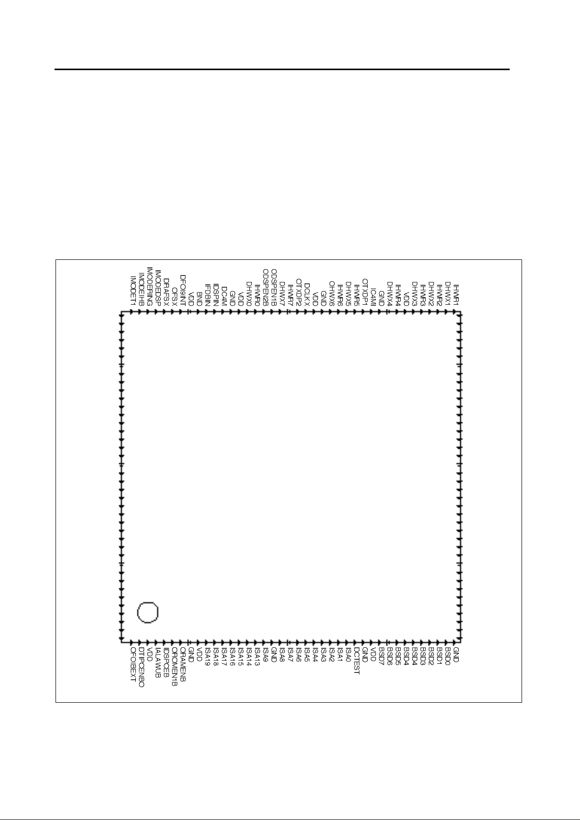
3-8 STL 7065
3-8-1 General
STL7065 is ASIC which performs various functions. It controls main system in COMPACT
System. But in COMPACT II(PLUS), it is used as DTMFR mode only at the MISC card.
3-8-2 Pin Map
121
160
ROMEN2B
DEXENB
ORSVB
OTEST7
OTEST6
OTEST5
GND
GND
OTEST4
OTEST3
OTEST2
OTEST1
OTEST0
VDD
ICODEEN
ITA7
ITA6
ITA5
ITA4
ITA3
ITA2
ITA2
ITA0
VDD
IC16M
GND
BDD
BTD7
BTD6
BTD5
BTD4
BTD3
BTD2
BTD1
BTD0
GND
ITRWB
OESFACKB
OEXFINTB
ITIPCENB
120
STL 7065
81
VDD
GND
GND
OLCOEN1B
OLCOEN2B
OLCOEN3B
OLCOEN4B
OLCOEN5B
OLCOEN6B
OLCOEN7B
OLINEENB
IPORB
OO4050M
ITIDET
OO10M
INMIB
GND
VDD
SISIOB
OCBM
IEXT2B
IEXT1B
OIPL0B
OIPL1B
OPL2B
GND
IFC0
IFC1
IFC2
OVECB
VDD
OC1K
OOAKB
ISRWB
ISDSB
ISASB
OINTIDB
GND
DEIPCENB
DESDENB
80
41
42
3-28
40
Page 29

3-9 Timing Chart
3-9-1 CLK
FOi
488n
FSx
CLKx
488nsec
4.096M
Chapter 3. IC Description & Timing
125µsec
244nsec
3-9-2 Processor
S0
CLK
FC2-FC0
A23-A0
AS
DS
R/W
DTACK
®Á
S1 S2 S3 S4 S5 S6 S7
®Ë
®È
®Í
®Î
®Ï
®Ì
®Ó
DATA OUT
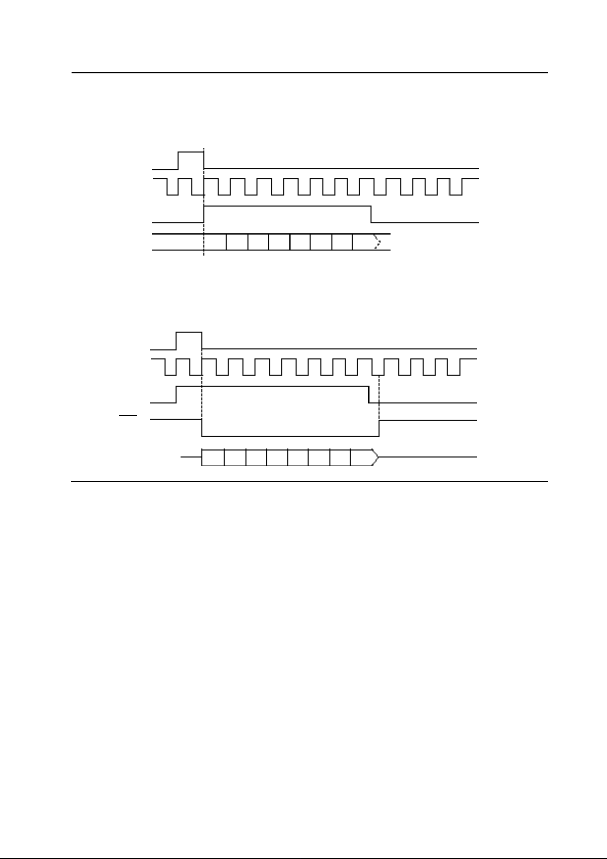
Write Cycle Timing
3-29
Page 30

Chapter 3. IC Description & Timing
min(ns) max(ns)
®Á £ ≠ 35
®Ë £ ≠ 35
®È 3 35
®Í 270 £ ≠
®Î 140 £ ≠
®Ï 5 £ ≠
®Ì 0 110
®Ó 40 £ ≠
S0
S1 S2 S3 S4 S5 S6 S7
CLK
FC2-FC0
®Á
A23-A0
®Ë
AS
DS
R/W
DTACK
DATA IN
®Î
CLK-8KHz:(S0+S1=125nsec)
min(ns) max(ns)
®Á £ ≠ 35
®Ë £ ≠ 35
®È 3 35
®Í 270 £ ≠
®Î 0 35
®Ï 5 £ ≠
®Ì 0 110
®Ó £ ≠ 90
®Ô 0 £ ≠
®È
®Í
®Ï
®Ó
®Ì
®Ô
Read Cycle Timing
3-30
Page 31
3-9-3 TMC
FSx
(2,048M)
CLKx
Time slot #0
Chapter 3. IC Description & Timing
Highway data
3-9-4 DMC
FSx
CLKx
Time slot #0
TSR
Highway data
D7 D6 D5 D4 D3 D2 D1 D0
D7 D6 D5 D4 D3 D2 D1 D0
3-31
 Loading...