


查询KMM5364005CSW供应商
DRAM MODULE KMM5364005CSW/CSWG
4Byte 4Mx36 SIMM
(4Mx16 & Quad CAS 4Mx4 base)
Revision 0.0
June 1999

DRAM MODULE KMM5364005CSW/CSWG
Revision History
Version 0.0 (June 1999)
• The 4th. generation of 64Mb DRAM components are applied for this module.
DRAM MODULE KMM5364005CSW/CSWG
KMM5364005CSW/CSWG EDO Mode
4M x 36 DRAM SIMM Using 4Mx16 & Quad CAS 4Mx4, 4K Refresh, 5V
GENERAL DESCRIPTION FEATURES
The Samsung KMM5364005C is a 4Mx36bits Dynamic RAM
high density memory module. The Samsung KMM5364005C
consists of two CMOS 4Mx16bits and one CMOS Quad CAS
4Mx4bits DRAMs in TSOP packages mounted on a 72-pin
glass-epoxy substrate. A 0.1 or 0.22uF decoupling capacitor
is mounted on the printed circuit board for each DRAM. The
KMM5364005C is a Single In-line Memory Module with edge
connections and is intended for mounting into 72 pin edge
connector sockets.
PERFORMANCE RANGE
Speed
-5 50ns 13ns 84ns 20ns
-6 60ns 15ns 104ns 25ns
tRAC tCAC tRC tHPC
• Part Identification
- KMM5364005CSW(4K cycles/64ms Ref, TSOP, Solder)
- KMM5364005CSWG(4K cycles/64ms Ref, TSOP, Gold)
• Extended Data Out Mode Operation
• CAS-before-RAS & Hidden Refresh capability
• RAS-only refresh capability
• TTL compatible inputs and outputs
• Single +5V±10% power supply
• JEDEC standard PDpin & pinout
• PCB : Height(1000mil), single sided component
PIN CONFIGURATIONS
Pin
10
11
12
13
14
15
16
17
18
19
20
21
22
23
24
25
26
27
28
29
30
31
32
33
34
35
36
Symbol
1
2
3
4
5
6
7
8
9
VSS
DQ0
DQ18
DQ1
DQ19
DQ2
DQ20
DQ3
DQ21
Vcc
NC
A0
A1
A2
A3
A4
A5
A6
A10
DQ4
DQ22
DQ5
DQ23
DQ6
DQ24
DQ7
DQ25
A7
A11
Vcc
A8
A9
NC
RAS2
DQ26
DQ8
Pin
37
38
39
40
41
42
43
44
45
46
47
48
49
50
51
52
53
54
55
56
57
58
59
60
61
62
63
64
65
66
67
68
69
70
71
72
Symbol
DQ17
DQ35
Vss
CAS0
CAS2
CAS3
CAS1
RAS0
NC
NC
W
NC
DQ9
DQ27
DQ10
DQ28
DQ11
DQ29
DQ12
DQ30
DQ13
DQ31
Vcc
DQ32
DQ14
DQ33
DQ15
DQ34
DQ16
NC
PD1
PD2
PD3
PD4
NC
Vss
PIN NAMES
Pin Name Function
A0 - A11 Address Inputs
DQ0 - 35 Data In/Out
W Read/Write Enable
RAS0, RAS2 Row Address Strobe
CAS0 - CAS3 Column Address Strobe
PD1 -PD4 Presence Detect
Vcc Power(+5V)
Vss Ground
NC No Connection
PRESENCE DETECT PINS (Optional)
Pin 50NS 60NS
PD1
PD2
PD3
PD4
SAMSUNG ELECTRONICS CO., LTD. reserves the right to
change products and specifications without notice.
Vss
NC
Vss
Vss
Vss
NC
NC
NC
DRAM MODULE KMM5364005CSW/CSWG
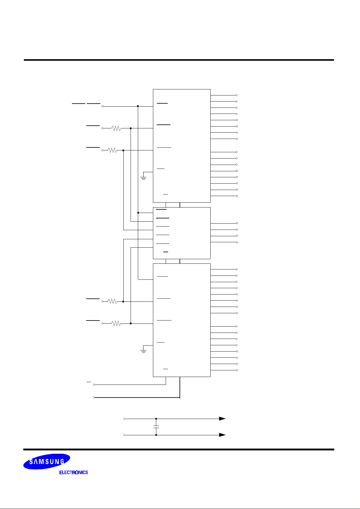
FUNCTIONAL BLOCK DIAGRAM
RAS0/RAS2
CAS0
CAS1
CAS2
CAS3
47Ω
47Ω
47Ω
47Ω
RAS
LCAS
UCAS
OE
W A0-A11
RAS
CAS0
CAS1
CAS2
CAS3
W A0-A11
RAS
LCAS
UCAS
OE
W A0-A11
U0
U1
U2
DQ0
DQ1
DQ2
DQ3
DQ4
DQ5
DQ6
DQ7
DQ8
DQ9
DQ10
DQ11
DQ12
DQ13
DQ14
DQ15
DQ0
DQ1
DQ2
DQ3
DQ0
DQ1
DQ2
DQ3
DQ4
DQ5
DQ6
DQ7
DQ8
DQ9
DQ10
DQ11
DQ12
DQ13
DQ14
DQ15
DQ0
DQ1
DQ2
DQ3
DQ4
DQ5
DQ6
DQ7
DQ9
DQ10
DQ11
DQ12
DQ13
DQ14
DQ15
DQ16
DQ8
DQ17
DQ26
DQ35
DQ18
DQ19
DQ20
DQ21
DQ22
DQ23
DQ24
DQ25
DQ27
DQ28
DQ29
DQ30
DQ31
DQ32
DQ33
DQ34
W
A0-A11
Vcc
Vss
0.1 or 0.22uF Capacitor
for each DRAM
To all DRAMs
DRAM MODULE KMM5364005CSW/CSWG
ABSOLUTE MAXIMUM RATINGS *
Item Symbol Rating Unit
Voltage on any pin relative to VSS
Voltage on VCC supply relative to VSS
Storage Temperature
Power Dissipation
Short Circuit Output Current
* Permanent device damage may occur if ABSOLUTE MAXIMUM RATINGS are exceeded. Functional operation should be restricted to
the conditions as detailed in the operational sections of this data sheet. Exposure to absolute maximum rating conditions for intended
periods may affect device reliability.
RECOMMENDED OPERATING CONDITIONS (Voltage referenced to VSS, TA = 0 to 70°C)
Item Symbol Min Typ Max Unit
Supply Voltage
Ground
Input High Voltage
Input Low Voltage
*1 : VCC+2.0V at pulse width≤20ns, which is measured at VCC.
*2 : -2.0V at pulse width≤ 20ns, which is measured at VSS.
DC AND OPERATING CHARACTERISTICS (Recommended operating conditions unless otherwise noted)
Symbol Speed
ICC1
ICC2 Don′t care - 6 mA
ICC3
ICC4
ICC5 Don′t care - 3 mA
ICC6
II(L)
IO(L)
VOH
VOL
-5
-6
-5
-6
-5
-6
-5
-6
Don′t care
Don′t care
VIN, VOUT
VCC
Tstg
Pd
IOS
VCC
VSS
VIH
VIL
KMM5364005CSW/CSWG
Min Max
-
-
-
-
-
-
-
-
-10
-5
2.4
-
4.5
2.4
-1.0
0
*2
-1 to +7.0
-1 to +7.0
-55 to +125
3
50
5.0
0
-
-
330
300
330
300
260
230
330
300
10
5
-
0.4
5.5
VCC
0.8
V
V
°C
W
mA
0
*1
V
V
V
V
Unit
mA
mA
mA
mA
mA
mA
mA
mA
uA
uA
V
V
ICC1
: Operating Current * (RAS, CAS, Address cycling @tRC=min)
ICC2
: Standby Current (RAS=CAS=W=VIH)
ICC3
: RAS Only Refresh Current * (CAS=VIH, RAS cycling @tRC=min)
ICC4
: Hyper Page Mode Current * (RAS=VIL, CAS cycling : tHPC=min)
ICC5
: Standby Current (RAS=CAS=W=Vcc-0.2V)
ICC6
: CAS-Before-RAS Refresh Current * (RAS and CAS cycling @tRC=min)
I(IL)
: Input Leakage Current (Any input 0≤VIN≤Vcc+0.5V, all other pins not under test=0 V)
I(OL)
: Output Leakage Current(Data Out is disabled, 0V≤VOUT≤Vcc)
: Output High Voltage Level (IOH = -5mA)
VOH
: Output Low Voltage Level (IOL = 4.2mA)
VOL
* NOTE : ICC1, ICC3, ICC4 and ICC6 are dependent on output loading and cycle rates. Specified values are obtained with the output open.
ICC is specified as an average current. In ICC1 and ICC3, address can be changed maximum once while RAS=VIL. In ICC4,
address can be changed maximum once within one EDO mode cycle time, tHPC.
DRAM MODULE KMM5364005CSW/CSWG
CAPACITANCE (TA = 25°C, VCC=5V, f = 1MHz)
Item Symbol Min Max Unit
Input capacitance[A0-A11]
Input capacitance[W]
Input capacitance[RAS0/RAS2]
Input capacitance[CAS0 - CAS3]
Input/Output capacitance[DQ0 - 35]
AC CHARACTERISTICS (0°C≤TA≤70°C, Vcc=5.0V±10%. See notes 1,2.)
Test condition : Vih/Vil=2.6/0.8V, Voh/Vol=2.0/0.8V, output loading CL=100pF
Parameter Symbol
Random read or write cycle time
Access time from RAS
Access time from CAS
Access time from column address
CAS to output in Low-Z
Output buffer turn-off delay from CAS
Transition time(rise and fall)
RAS precharge time
RAS pulse width
RAS hold time
CAS hold time
CAS pulse width
RAS to CAS delay time
RAS to column address delay time
CAS to RAS precharge time
Row address set-up time
Row address hold time
Column address set-up time
Column address hold time
Column address to RAS lead time
Read command set-up time
Read command hold referenced to CAS
Read command hold referenced to RAS
Write command set-up time
Write command hold time
Write command pulse width
Write command to RAS lead time
Write command to CAS lead time
Data set-up time
Data hold time
Refresh period
CAS setup time (CAS-before-RAS refresh)
CAS hold time (CAS-before-RAS refresh)
RAS to CAS precharge time
Access time from CAS precharge
tRC
tRAC
tCAC
tAA
tCLZ
tCEZ
tT
tRP
tRAS
tRSH
tCSH
tCAS
tRCD
tRAD
tCRP
tASR
tRAH
tASC
tCAH
tRAL
tRCS
tRCH
tRRH
tWCS
tWCH
tWP
tRWL
tCWL
tDS
tDH
tREF
tCSR
tCHR
tRPC
tCPA
CIN1
CIN2
CIN3
CIN4
CDQ
-5 -6
Min Max Min Max
84 104 ns
3 3 ns 3
3 13 3 13 ns 6,12
1 50 1 50 ns 2
30 40 ns
50 10K 60 10K ns
13 15 ns
38 45 ns
8 10K 10 10K ns 4
20 37 20 45 ns 9
15 25 15 30 ns
5 5 ns
0 0 ns
10 10 ns
0 0 ns
8 10 ns
25 30 ns
0 0 ns
0 0 ns 8
0 0 ns 8
0 0 ns 7
10 10 ns
10 10 ns
13 15 ns
8 10 ns
0 0 ns 9
8 10 ns 9
5 5 ns
10 10 ns
5 5 ns
-
-
-
-
-
50 60 ns 3,4,10
13 15 ns 3,4,5
25 30 ns 3,10
64 64 ms
28 35 ns 3
25
31
31
24
17
pF
pF
pF
pF
pF
Unit Note
DRAM MODULE KMM5364005CSW/CSWG
AC CHARACTERISTICS (0°C≤TA≤70°C, Vcc = 5.0V±10%. See notes 1,2.)
Test condition : Vih/Vil=2.6/0.8V, Voh/Vol=2.0/0.8V, output loading CL=100pF
Parameter Symbol
Hyper page mode cycle time
CAS precharge time (Hyper page cycle)
RAS pulse width (Hyper page cycle)
RAS hold time from CAS precharge
W to RAS precharge time(C-B-R refresh)
W to RAS hold time(C-B-R refresh)
Output data hold time
Output buffer turn off delay from RAS
Output buffer turn off delay from W
W to data delay
W pulse width
NOTES
An initial pause of 200us is required after power-up followed
1.
by any 8 RAS-only or CAS-before-RAS refresh cycles before
proper device operation is achieved.
2.
Input voltage levels are Vih/Vil. VIH(min) and VIL(max) are reference levels for measuring timing of input signals. Transition
times are measured between VIH(min) and VIL(max) and are
assumed to be 5ns for all inputs.
3.
Measured with a load equivalent to 2 TTL loads and 100pF.
tHPC
tCP
tRASP
tRHCP
tWRP
tWRH
tDOH
tREZ
tWEZ
tWED
tWPE
-5 -6
Min Max Min Max
20 25 ns 11
8 10 ns
50 200K 60 200K ns
30 35 ns
10 10 ns
10 10 ns
5 5 ns
3 13 3 15 ns 6,12
3 13 3 15 ns 6
15 15 ns
5 5 ns
8.
Either tRCH or tRRH must be satisfied for a read cycle.
9.
These parameters are referenced to the CAS leading edge in
early write cycles.
Operation within the tRAD(max) limit insures that tRAC(max)
10.
can be met. tRAD(max) is specified as reference point only. If
Unit Note
tRAD is greater than the specified tRAD(max) limit access time
is controlled by tAA.
4.
Operation within the tRCD(max) limit insures that tRAC(max)
can be met. tRCD(max) is specified as a reference point only.
If tRCD is greater than the specified tRCD(max) limit, then
access time is controlled exclusively by tCAC.
5.
Assumes that tRCD≥tRCD(max).
6.
This parameter defines the time at which the output achieves
the open circuit and is not referenced for VOH or VOL
tWCS is non-restrictive operating parameter. It is included in
7.
the data sheet as electrical characteristics only. If
tWCS≥tWCS(min), the cycle is an early write cycle and the
data out pin will remain high impedance for the duration of
the cycle.
tASC≥6ns, Assume tT=2.0ns.
11.
12.
If RAS goes high before CAS high going, the open circuit
condition of the output is achieved by CAS high going. If CAS
goes high before RAS high going , the open circuit condition
of the output is achieved by RAS going.
DRAM MODULE KMM5364005CSW/CSWG
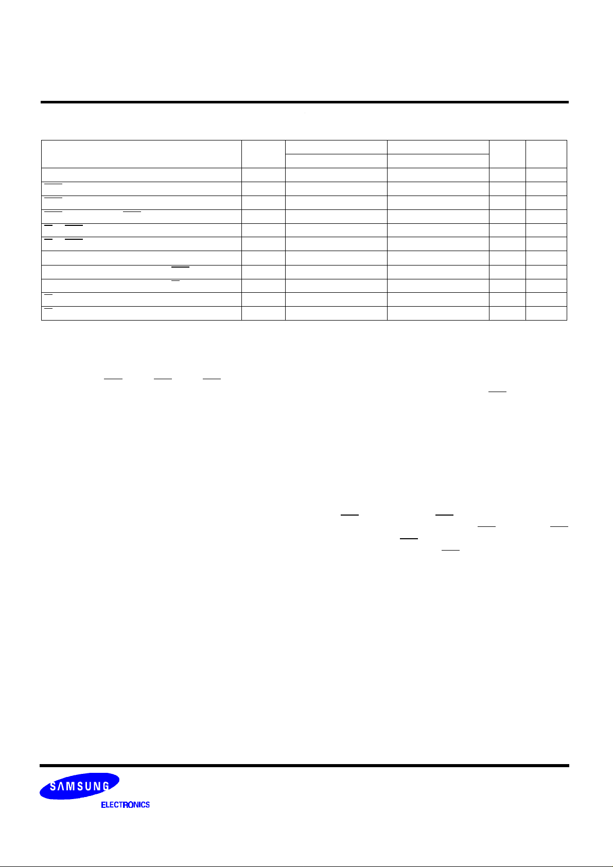
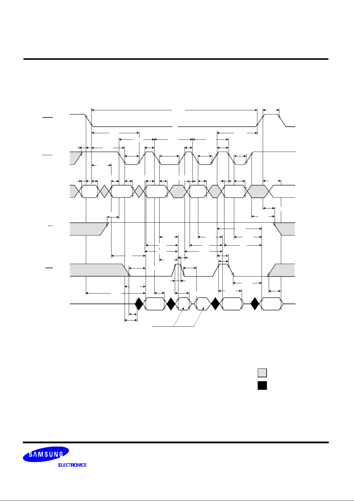
READ CYCLE
RAS
CAS
OE
DQ
A
W
VIH -
VIL -
VIH -
VIL -
VIH -
VIL -
VIH -
VIL -
VIH -
VIL -
VOH -
VOL -
tCRP
tRAD
tASR tRAH tASC
ROW
ADDRESS
tRCS
OPEN
tRAC
tRAS
tCSH
tCAH
COLUMN
ADDRESS
tCLZ
tAA
tOEA
tCAC
tRC
tCAS
tRAL
tOLZ
tRP
tRSHtRCD
tCRP
tRCH
tRRH
tWEZ
tCEZ
tOEZ
tREZ
DATA-OUT
Don′t care
Undefined
DRAM MODULE KMM5364005CSW/CSWG
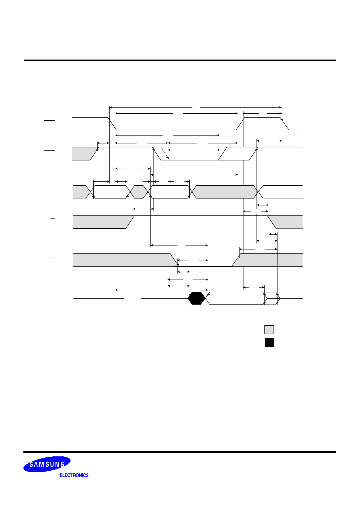
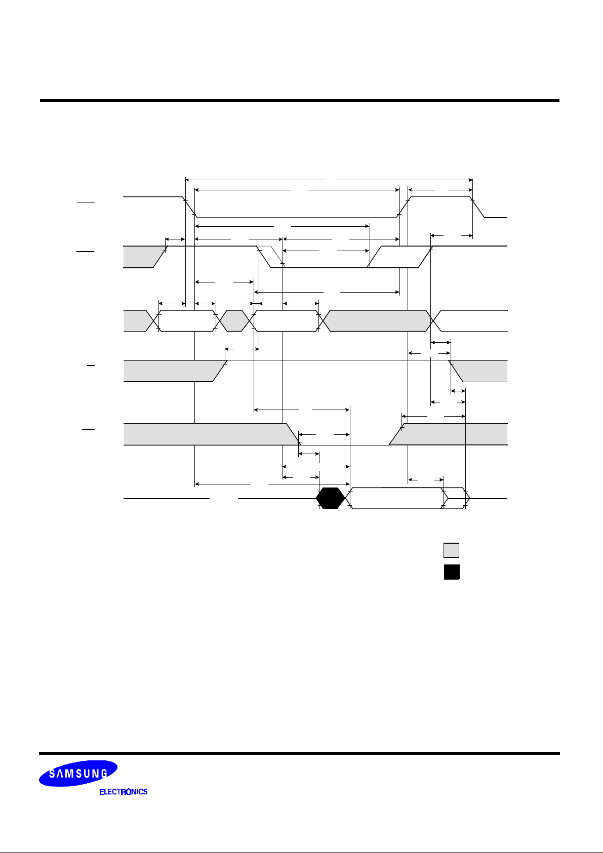
WRITE CYCLE ( EARLY WRITE )
NOTE : DOUT = OPEN
RAS
CAS
OE
DQ
W
A
VIH -
VIL -
VIH -
VIL -
VIH -
VIL -
VIH -
VIL -
VIH -
VIL -
VIH -
VIL -
tCRP
tRAD
tASR tRAH tASC
ROW
ADDRESS
tWCS
tDS
tCSH
COLUMN
ADDRESS
tWP
DATA-IN
tRAS
tCAH
tCWL
tWCH
tDH
tCAS
tRWL
tRC
tRAL
tRP
tRSHtRCD
tCRP
Don′t care
Undefined
DRAM MODULE KMM5364005CSW/CSWG
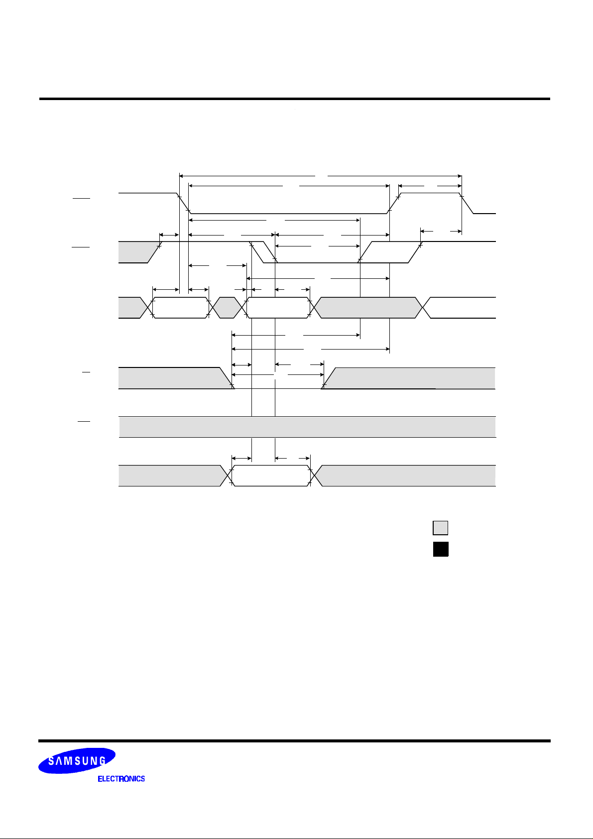
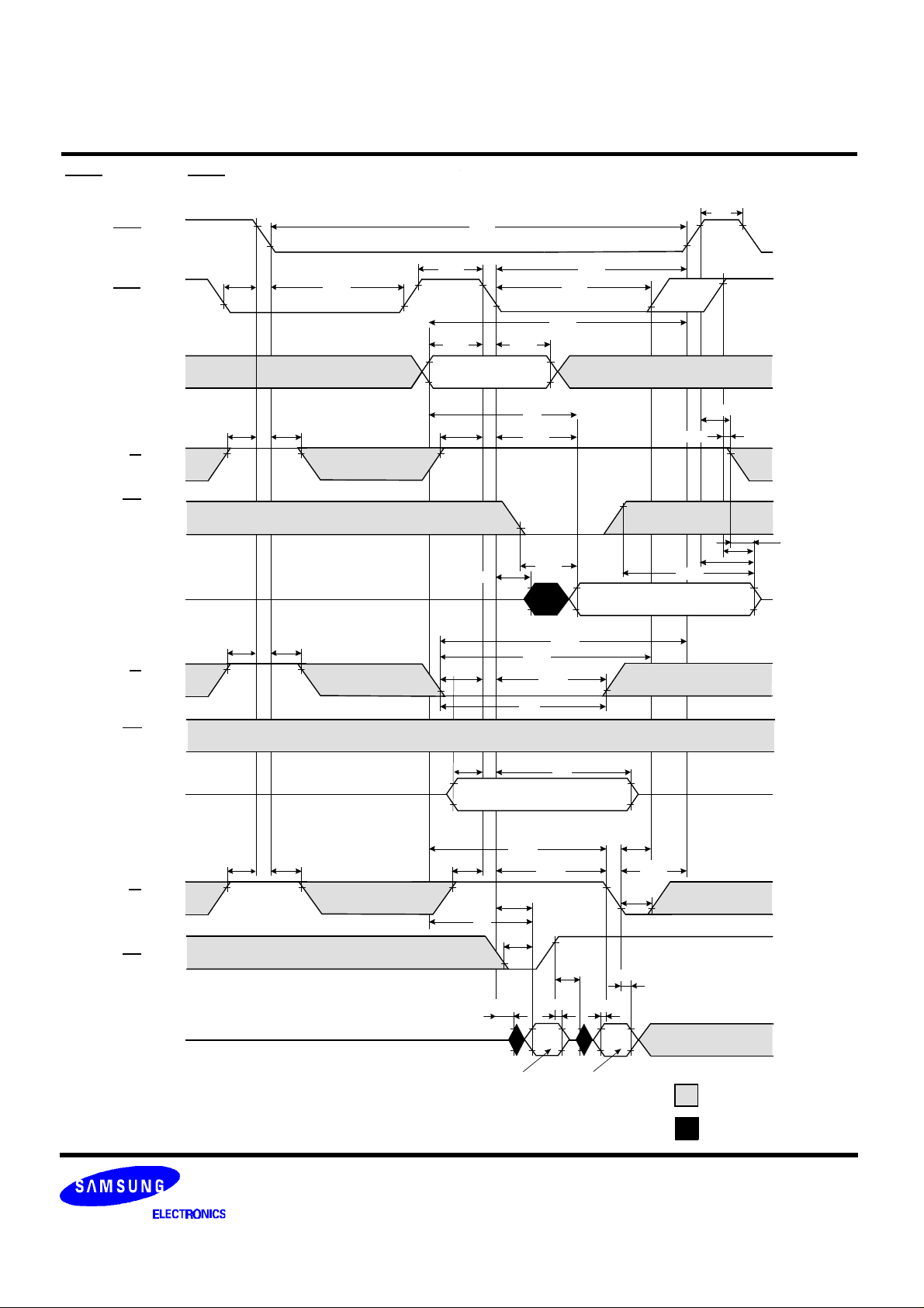
WRITE CYCLE ( OE CONTROLLED WRITE )
NOTE : DOUT = OPEN
RAS
CAS
W
OE
DQ
A
VIH -
VIL -
VIH -
VIL -
VIH -
VIL -
VIH -
VIL -
VIH -
VIL -
VIH -
VIL -
tCRP
tRAD
tASR tRAH tASC
ROW
ADDRESS
tOED
tRAS
tCSH
tCAH
COLUMN
ADDRESS
tDS
DATA-IN
tWP
tOEH
tDH
tRC
tRSHtRCD
tCAS
tRAL
tCWL
tRP
tCRP
tRWL
Don′t care
Undefined

DRAM MODULE KMM5364005CSW/CSWG
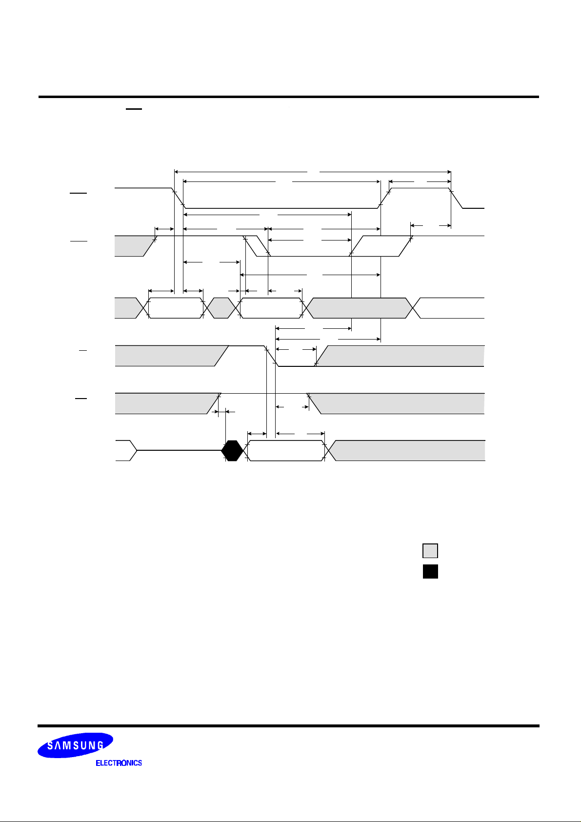
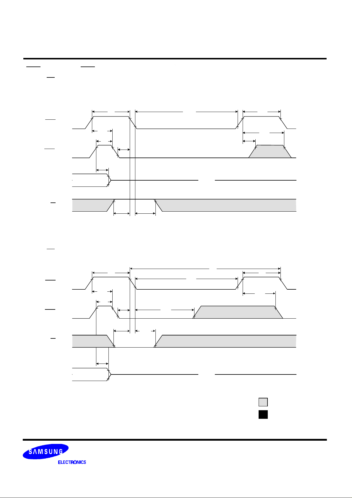
READ - MODIFY - WRITE CYCLE
RAS
CAS
OE
DQ
A
W
VI/OH -
VI/OL -
VIH -
VIL -
VIH -
VIL -
VIH -
VIL -
VIH -
VIL -
VIH -
VIL -
tCRP
tRAD
tASR tRAH tASC tCAH
ROW
ADDR
COLUMN
ADDRESS
tOEA
tOLZ
tCLZ
tCAC
tAA
tRAC
tRWD
tRAS
tAWD
tCWD
VALID
DATA-OUT
tRWC
tRSHtRCD
tOED
tOEZ
tCAS
tCSH
tWP
tDS tDH
VALID
DATA-IN
tRP
tRWL
tCWL
Don′t care
Undefined
DRAM MODULE KMM5364005CSW/CSWG
HYPER PAGE READ CYCLE
RAS
CAS
OE
DQ
A
W
VIH -
VIL -
VIH -
VIL -
VIH -
VIL -
VIH -
VIL -
VIH -
VIL -
VOH -
VOL -
tCRP
tASR
tRASP
¡ó
tCSH
tHPC tHPC tHPC
tRCD
tCP tCP tCP
tCAS tCAS tCAS tCAS
tRAD
tRAH tASC tCAH tCAH tCAH tASC tCAH
ROW
ADDR
COLUMN
ADDRESS
tASC
COLUMN
ADDRESS
tASC
COLUMN
ADDR
tRCS
tAA
tCAC
tAA
tCPA
tCAC
tOEA
tCAC
tAA
tCPA
tOCH
tOEA
tOEP
tCAC
tRAC
tOLZ
tCLZ
tDOH
VALID
DATA-OUT
VALID
DATA-OUT
tOEZ
tRHCP
COLUMN
ADDRESS
tCPA
tCHO
tOEP
tOEZ
VALID
DATA-OUT
tAA
tOEA
tCAC
tRCH
VALID
DATA-OUT
tRP
tREZ
tRRH
tOEZ
Don′t care
Undefined
DRAM MODULE KMM5364005CSW/CSWG
READ CYCLE
RAS
CAS
OE
DQ
A
W
VIH -
VIL -
VIH -
VIL -
VIH -
VIL -
VIH -
VIL -
VIH -
VIL -
VOH -
VOL -
tCRP
tRAD
tASR tRAH tASC
ROW
ADDRESS
tRCS
OPEN
tRAC
tRAS
tCSH
tCAH
COLUMN
ADDRESS
tCLZ
tAA
tOEA
tCAC
tRC
tCAS
tRAL
tOLZ
tRP
tRSHtRCD
tCRP
tRCH
tRRH
tWEZ
tCEZ
tOEZ
tREZ
DATA-OUT
Don′t care
Undefined

DRAM MODULE KMM5364005CSW/CSWG
HYPER PAGE READ-MODIFY-WRITE CYCLE
RAS
CAS
OE
DQ
A
W
VI/OH -
VI/OL -
VIH -
VIL -
VIH -
VIL -
VIH -
VIL -
VIH -
VIL -
VIH -
VIL -
tCRP
tASR
ROW
ADDR
tRCD
tRAD
tASC
tRAH
tRAC
tCLZ
COL.
ADDR
tRCS
tCSH
tRASP
tCP
tCAS tCAS
tCAH
tASC
ADDR
tCWL
tWP
tCWD
tAWD
tRWD
tOEA
tOED
tCAC
tAA
tOEZ
tDS
tDH
tCAC
tCLZ
tOLZ
VALID
DATA-OUT
VALID
DATA-IN
COL.
tAA
tCAH
tCPWD
tOEA
tAWD
tOLZ
tHPRWC
tCWD
tOEZ
tRSH
tRAL
tRWL
tCWL
tOED
VALID
DATA-OUT
tWP
tDS
tDH
VALID
DATA-IN
tRP
tCRP
Don′t care
Undefined

DRAM MODULE KMM5364005CSW/CSWG
HYPER PAGE READ AND WRITE MIXED CYCLE
RAS
CAS
DQ
A
W
OE
VIH -
VIL -
VIH -
VIL -
VIH -
VIL -
VIH -
VIL -
VIH -
VIL -
VI/OH -
VI/OL -
tRAD
tASR
READ(tCAC) READ(tCPA)
tCAS
tRAH
tASC tCAH tCAH
ROW
ADDR
COLUMN
ADDRESS
tOEA
tCAC
tAA
tRAC
tRASP
WRITE
READ(tAA)
tHPC tHPC tHPC
tCP
tASC
COLUMN
ADDRESS
tRCHtRCS tRCS tRCH
tCP tCP
tCAStCAS
tASC
tCAH
COL.
ADDR
tRCH tWCH
tCAS
tASC tCAH
COL.
ADDR
tWCS
tWPE
tCLZ
tWEZ
VALID
DATA-OUT
tCPA
tWEZ
VALID
DATA-OUT
tWED
tDH
tDS
VALID
DATA-IN
tAA
VALID
DATA-OUT
tRP
tREZ
Don′t care
Undefined

DRAM MODULE KMM5364005CSW/CSWG
RAS - ONLY REFRESH CYCLE*
NOTE : W, OE, DIN = Don′t care
DOUT = OPEN
VIH -
RAS
VIL -
tCRP
VIH -
CAS
A
VIL -
VIH -
VIL -
tASR
tRAH
ROW
ADDR
CAS - BEFORE - RAS REFRESH CYCLE
NOTE : OE , A = Don′t care
tRP
VIH -
RAS
CAS
VIL -
VIH -
VIL -
tRPC
tCP
tCSR
tCHR
tRAS
tRC
tRAS
tRC
tRP
tRPC tCRP
tRP
tRPC
W
tWRP
VIH -
VIL -
tWRH
tCEZ
VOH -
DQ
VOL -
* In RAS-only refresh cycle of 64Mb A-dile & B-die, when CAS signal transits from Low to High, the valid data may be cut off.
OPEN
Don′t care
Undefined

DRAM MODULE KMM5364005CSW/CSWG
HIDDEN REFRESH CYCLE ( READ )
RAS
CAS
W
OE
DQ
A
VIH -
VIL -
VIH -
VIL -
VIH -
VIL -
VIH -
VIL -
VIH -
VIL -
VOH -
VOL -
tCRP
tRAD
tASR tRAH tASC
ROW
ADDRESS
tRCS
OPEN
tRC
tRAS
COLUMN
ADDRESS
tCLZ
tRAC
tCAH
tAA
tOEA
tOLZ
tCAC
tRRH
tRP
tCHRtRCD tRSH
tWRH
tWRP
DATA-OUT
tRC
tRAS
tOEZ
tRP
tCEZ
tREZ
tWEZ
Don′t care
Undefined

DRAM MODULE KMM5364005CSW/CSWG
HIDDEN REFRESH CYCLE ( WRITE )
NOTE : DOUT = OPEN
RAS
CAS
OE
DQ
W
A
VIH -
VIL -
VIH -
VIL -
VIH -
VIL -
VIH -
VIL -
VIH -
VIL -
VIH -
VIL -
tCRP
tRAD
tASR tRAH tASC
ROW
ADDRESS
tWCS
tDS
tRC
tRAS
COLUMN
ADDRESS
DATA-IN
tWP
tCAH
tWCH
tDH
tRP
tRC
tRP
tRAS
tRSHtRCD
tCHR
tWRH
tWRP
Don′t care
Undefined
DRAM MODULE KMM5364005CSW/CSWG
CAS-BEFORE-RAS REFRESH COUNTER TEST CYCLE
tRP
RAS
CAS
A
VIH -
VIL -
VIH -
VIL -
VIH -
VIL -
tCSR
tCHR
tRAS
tCPT
tASC tCAH
COLUMN
ADDRESS
tRSH
tCAS
tRAL
READ CYCLE
VIH -
W
VIL VIH -
OE
VIL -
VOH -
DQ
VOL -
WRITE CYCLE
VIH -
W
VIL -
VIH -
OE
VIL -
VIH -
DQ
VIL -
tWRP tWRH
tWRP tWRH
READ-MODIFY-WRITE
tWRP tWRH
VIH -
W
VIL -
VIH -
OE
VIL -
tRCS
tWCS
tDS
tRCS
tCLZ
tAA
tWP
DATA-IN
tAWD
tCAC
tOEA
tAA
tCAC
tOEA
tCWL
tCWD
tRWL
tWCH
tDH
tOED
DATA-OUT
tRWL
tWP
tDH
tCWL
tRCH
tOEZ
tRRH
tCEZ
tREZ
tWEZ
tCLZ tOEZ
VI/OH -
DQ
VI/OL -
VALID
DATA-OUT
NOTE : This timing diagram is applied to all devices besides 64M DRAM based modules.
VALID
DATA-IN
tDS
Don′t care
Undefined
DRAM MODULE KMM5364005CSW/CSWG
CAS - BEFORE - RAS SELF REFRESH CYCLE
NOTE : OE, A = Don′t care
VIH -
RAS
VIL -
VIH -
CAS
VIL -
tCEZ
VOH -
DQ
VOL -
VIH -
W
VIL -
TEST MODE IN CYCLE
NOTE : OE , A = Don′t care
VIH -
RAS
VIL -
VIH -
CAS
VIL -
tRPC
tCP
tRPC
tCP
tRP
tCSR
tWRP tWRH
tRP
tCSR
tCHR
tRASS
tRAS
OPEN
tRC
tRPS
tRPC
tCHS
tRP
tRPC
DQ
W
VIH -
VIL -
VOH VOL -
tCEZ
tWTS
tWTH
OPEN
Don′t care
Undefined

DRAM MODULE KMM5364005CSW/CSWG
PACKAGE DIMENSIONS
Units : Inches (millimeters)
4.250(107.95)
3.984(101.19)
.133(3.38)
1.000(25.40)
.250(6.35)
.125 DIA±.002(3.18±.051)R.062(1.57)
.400(10.16)
.080(2.03)
.250(6.35)
.010(.25)MAX
.250(6.35)
3.750(95.25)
( Front view )
( Back view )
Gold/Solder Plating Lead
.050(1.27)
.041±.004(1.04±.10)
R.062±.004(R1.57±.10)
.054(1.37)
.047(1.19)
.100(2.54)
MAX
0.125
(3.20MIN)
MIN
Tolerances : ±.005(.13) unless otherwise specified
NOTE : The used device is 4Mx16 & Quad CAS 4Mx4 DRAM, TSOPII
DRAM Part No. : KMM5364005CSW/CSWG -- KM416C4104CS & KM44C4005CS(300 mil)
 Loading...