

SAMSUNG KM6164002, KM6164002E, KM6164002I Technical data

查询KM6164002供应商
PRELIMINARY
KM6164002, KM6164002E, KM6164002I CMOS SRAM
PACKAGE DIMENSIONS
44-SOJ-400
11.18±0.12
0.440±0.005
0.95
( )
0.0375
#44
#1
0.43
0.017
+0.10
-0.05
+0.004
-0.002
28.98
MAX
1.141
25.58±0.12
1.125±0.005
1.27
0.050
0.71
0.028
+0.10
-0.05
+0.004
-0.002
#23
#22
Units : Inches (millimeters)
10.16
0.400
0.69
MIN
0.027
1.19
( )
0.047
3.76
MAX
0.148
1.27
( )
0.050
9.40±0.25
0.370±0.010
0.20
0.008
0.10
MAX
0.004
+0.10
-0.05
+0.004
-0.002
- 9 -
Rev 2.0
June -1997
PRELIMINARY
KM6164002, KM6164002E, KM6164002I CMOS SRAM
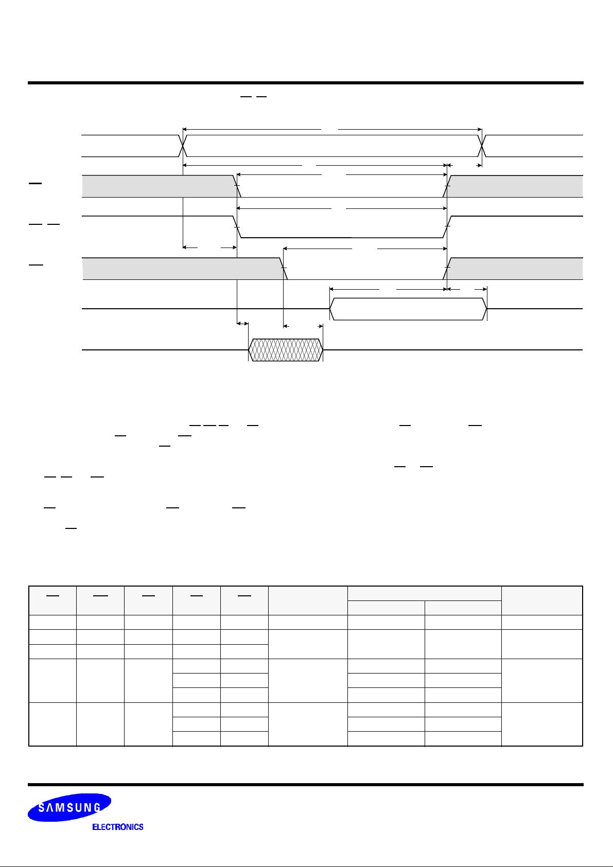
TIMING WAVE FORM OF WRITE CYCLE(4) (UB, LB Controlled)
tWC
ADD
tAW
tCW(3)
CS
tBW
UB, LB
tWR(5)
tAS(4)
WE
Data In
Data Out
NOTES (WRITE CYCLE)
1. All write cycle timing is referenced from the last valid address to the first transition address.
2. A write occurs during the overlap of a low CS,WE,LB and UB. A write begins at the latest transition CS going low and WE going low ; A write ends at
the earliest transition CS going high or WE going high. tWP is measured from the beginning of write to the end of write.
3. tCW is measured from the later of CS going low to end of write.
4. tAS is measured from the address valid to the beginning of write.
5. tWR is measured from the end of write to the address change. t WR applied in case a write ends as CS, or WE going high.
6. If OE. CS and WE are in the Read Mode during this period, the I/O pins are in the output low-Z state. Inputs of opposite phase of the output mus t not
be applied because bus contention can occur.
7. For common I/O applications, minimization or elimination of bus contention conditions is necessary during read and write cycl e.
8. If CS goes low simultaneously with WE going or after WE going low, the outputs remain high impedance state.
9. Dout is the read data of the new address.
10. When CS is low : I/O pins are in the output state. The input signals in the opposite phase leading to the output should not be applied.
High-Z
High-Z
tBLZ
tWHZ(6)
tWP(2)
tDW tDH
Data Valid
High-Z(8)
FUNCTIONAL DESCRIPTION
CS WE OE LB UB Mode
H X X* X X Not Select High-Z High-Z ISB, ISB1
L H H X X
L X X H H
L H
L H L
L L X
* NOTE : X means Don't Care.
H L High-Z DOUT
L L DOUT DOUT
L H
H L High-Z DIN
L L DIN DIN
Output Disable High-Z High-Z ICC
Read
Write
- 8 -
I/O1~I/O8 I/O9~I/O16
DOUT High-Z
I/O Pin
DIN High-Z
Supply Current
ICC
ICC
Rev 2.0
June -1997
PRELIMINARY
KM6164002, KM6164002E, KM6164002I CMOS SRAM
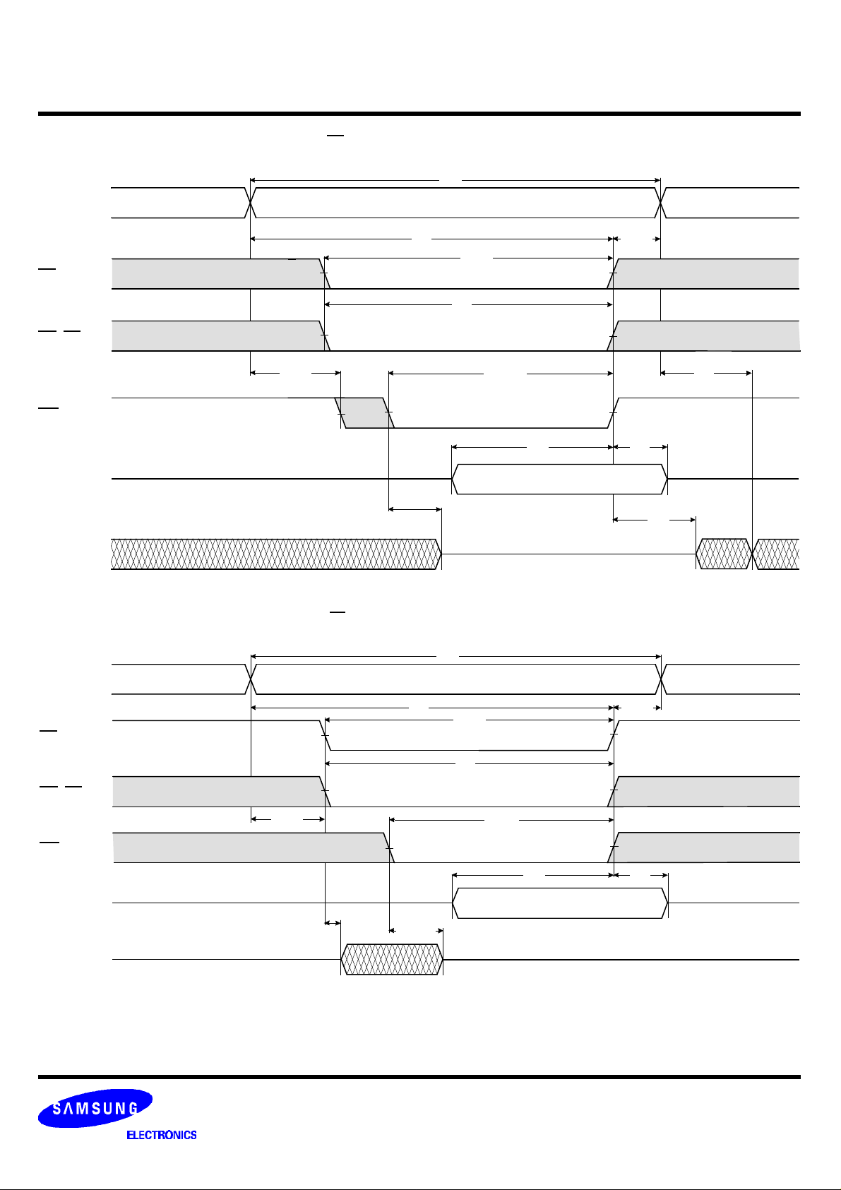
TIMING WAVE FORM OF WRITE CYCLE(2) (OE=Low Fixed)
tWC
ADD
CS
UB, LB
tAS(4)
WE
Data In
Data Out
High-Z
TIMING WAVE FORM OF WRITE CYCLE(3) (CS=Controlled)
tAW
tWHZ(6)
tCW(3)
tBW
tWP1(2)
High-Z
tWR(5)
tDW tDH
Data Valid
tOW
tOH
(10) (9)
ADD
CS
UB, LB
WE
Data In
Data Out
High-Z
High-Z
tAS(4)
tLZ
tAW
tWHZ(6)
tWC
tCW(3)
tBW
tWP(2)
tDW
Data Valid
tWR(5)
tDH
High-Z(8)
- 7 -
Rev 2.0
June -1997
 Loading...