

Samsung KM4132G271BQ-10, KM4132G271BTQ-8, KM4132G271BQR-8, KM4132G271BQR-7, KM4132G271BQR-10 Datasheet
...
KM4132G271B CMOS SGRAM
- 1 -
Rev. 2.4 (May 1998)
Revision 2.4
May 1998
8Mbit SGRAM
128K x 32bit x 2 Banks
Synchronous Graphic RAM
LVTTL
Samsung Electronics reserves the right to change products or specification without notice.

KM4132G271B CMOS SGRAM
- 2 -
Rev. 2.4 (May 1998)
Revision History
Revision 2.4 (May 1998)
• Added KM4132G271B-7 product(143MHz @ CL =3).
Revision 2.3 (March 1998)
• Added Reverse Type Package in ODERING INFORMATION and PIN CONFIGURATION.
• Removed KM4132G271B-H/12 product(-H : 100MHz @ CL =2, -12 : 83MHz @ CL=3).
• Changed the Current values of ICC1, ICC3N, ICC4, ICC5, ICC6, ICC7 in DC CHARACTERISTICS.
• Changed tSAC from 6 to 6.5 @ 125MHz, tSS from 2 to 2.5 @ 125MHz in AC PARAMETER .
• Delete a page including FREQUENCY vs. AC PARAMETER RELATIONSHIP TABLE.
Revision 2.1 (November 1997)
• Changed the Height of TQFP Package from 1.4mmMAX to 1.2mmMax in PACKAGE DIMENSIONS.
Revision 2.0 (October 1997)
• Added -H binning(100MHz @ CL =2 ).
• Changed some values in DC CHARACTERISTICS.
• Changed some values in AC PARAMETER (tSAC / tOH / tSHZ / tRP / tRC / tBPL / tBWC etc.).
• Removed a AC Parameter, tBAL(Block write data-in to Active command period) in AC PARAMETER .
• Changed some values in FREQUENCY vs. AC PARAMETER RELATIONSHIP TABLE.
• Added the Package Type description(PQFP, TQFP) in PACKAGE DIMENSIONS.
KM4132G271B CMOS SGRAM
- 3 -
Rev. 2.4 (May 1998)
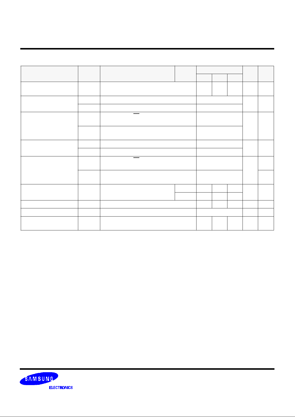
The KM4132G271B is 8,388,608 bits synchronous high data
rate Dynamic RAM organized as 2 x 131,072 words by 32 bits,
fabricated with SAMSUNG's high performance CMOS technology. Synchronous design allows precise cycle control with the
use of system clock. I/O transactions are possible on every
clock cycle. Range of operating frequencies, programmable
burst length, and programmable latencies allows the same
device to be useful for a variety of high bandwidth, high performance memory system applications.
Write per bit and 8 columns block write improves performance in
graphics systems.
• JEDEC standard 3.3V power supply
• LVTTL compatible with multiplexed address
• Dual bank / Pulse RAS
• MRS cycle with address key programs
-. CAS Latency (2, 3)
-. Burst Length (1, 2, 4, 8 & full page)
-. Burst Type (Sequential & Interleave)
• All inputs are sampled at the positive going edge of the
system clock
• Burst Read Single-bit Write operation
• DQM 0-3 for byte masking
• Auto & self refresh
• 16ms refresh period (1K cycle)
• 100 Pin PQFP, TQFP (14 x 20 mm)
• Reverse Type Package offers the best signal routing
Graphics Features
• SMRS cycle.
-. Load mask register
-. Load color register
• Write Per Bit(Old Mask)
• Block Write(8 Columns)
GENERAL DESCRIPTIONFEATURES
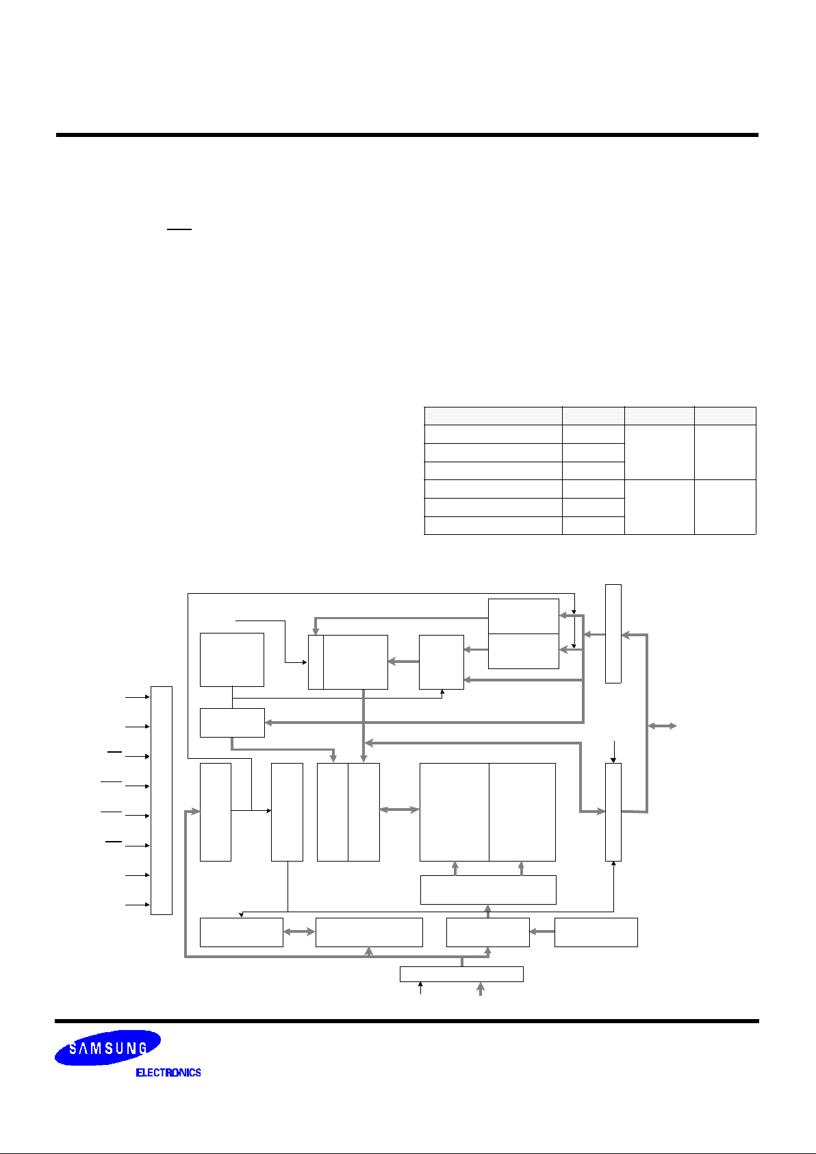
FUNCTIONAL BLOCK DIAGRAM
128K x 32Bit x 2 Banks Synchronous Graphic RAM
TIMING REGISTER
CLK
CKE
CS
RAS
CAS
WE
DSF
DQMi
BLOCK
WRITE
CONTROL
LOGIC
DQi
PROGRAMING
REGISTER
LATENCY &
BURST LENGTH
128Kx32
CELL
ARRAY
128Kx32
CELL
ARRAY
SERIAL
COUNTER
COLUMN ADDRESS
BUFFER
ROW DECORDER
BANK SELECTION
ADDRESS REGISTER
REFRESH
COUNTER
ROW ADDRESS
BUFFER
INPUT BUFFER
MASK
REGISTER
COLOR
REGISTER
MUX
WRITE
CONTROL
LOGIC
MASK
COLUMN
DECORDER
SENSE
AMPLIFIER
COLUMN
MASK
(i=0~31)DQMi
CLOCK ADDRESS(A0~A9)
DQMi
OUTPUT BUFFER
•
•
•
ORDERING INFORMATION
* ~G271BQR# / ~G271BTQR# : Reverse Type Package
Part NO. Max Freq. Interface Package
KM4132G271BQ(R)-7 143MHz
LVTTL 100 PQFP KM4132G271BQ(R)-8 125MHz
KM4132G271BQ(R)-10 100MHz
KM4132G271BTQ(R)-7 143MHz
LVTTL 100 TQFP KM4132G271BTQ(R)-8 125MHz
KM4132G271BTQ(R)-10 100MHz
KM4132G271B CMOS SGRAM
- 4 -
Rev. 2.4 (May 1998)
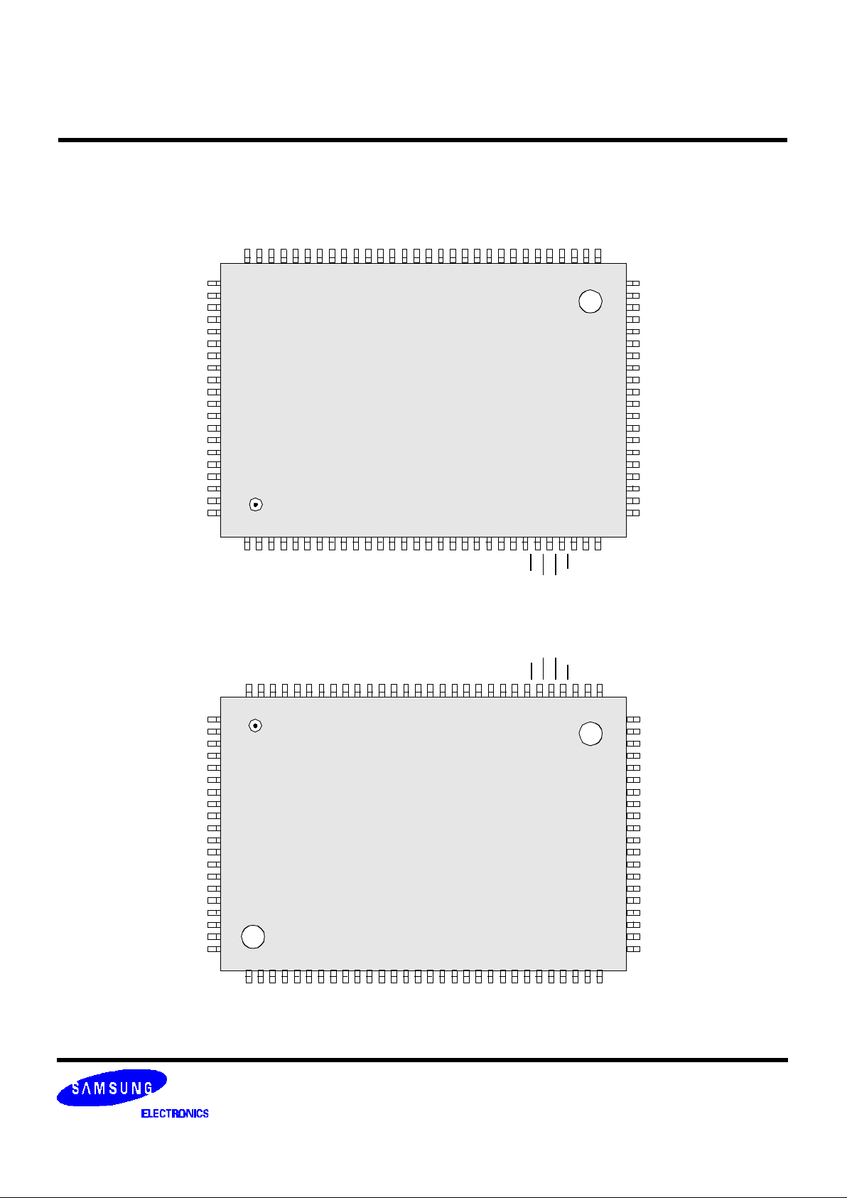
DQ29
VSSQ
DQ30
DQ31
VSS
N.C
N.C
N.C
N.C
N.C
N.C
N.C
N.C
N.C
N.C
VDD
DQ0
DQ1
VSSQ
DQ2
81
82
83
84
85
86
87
88
89
90
91
92
93
94
95
96
97
98
99
100
PIN CONFIGURATION (TOP VIEW)
DQ3
VDDQ
DQ4
DQ5
VSSQ
DQ6
DQ7
VDDQ
DQ16
DQ17
VSSQ
DQ18
DQ19
VDDQ
VDD
VSS
DQ20
DQ21
VSSQ
DQ22
DQ23
VDDQ
DQM0
DQM2
WE
CAS
RAS
CS
BA(A9)
N.C
1234567891011121314151617181920212223242526272829
30
A7
A6
A5
A4
VSS
N.C
N.C
N.C
N.C
N.C
N.C
N.C
N.C
N.C
N.C
VDD
A3
A2
A1
A0
50
49
48
47
46
45
44
43
42
41
40
39
38
37
36
35
34
33
32
31
100 Pin QFP
Forward Type
20 x 14
§±
0.65§® pin Pitch
Forward Type
DQ28
VDDQ
DQ27
DQ26
VSSQ
DQ25
DQ24
VDDQ
DQ15
DQ14
VSSQ
DQ13
DQ12
VDDQ
VSS
VDD
DQ11
DQ10
VSSQ
DQ9
DQ8
VDDQ
N.C
DQM3
DQM1
CLK
CKE
DSF
N.C
A8
8079787776757473727170696867666564636261605958575655545352
51
Reverse Type
DQ2
VSSQ
DQ1
DQ0
VDD
N.C
N.C
N.C
N.C
N.C
N.C
N.C
N.C
N.C
N.C
VSS
DQ31
DQ30
VSSQ
DQ29
100
99
98
97
96
95
94
93
92
91
90
89
88
87
86
85
84
83
82
81
DQ3
VDDQ
DQ4
DQ5
VSSQ
DQ6
DQ7
VDDQ
DQ16
DQ17
VSSQ
DQ18
DQ19
VDDQ
VDD
VSS
DQ20
DQ21
VSSQ
DQ22
DQ23
VDDQ
DQM0
DQM2WECAS
RASCSBA(A9)
N.C
123456789
101112131415161718192021222324252627282930
A0
A1
A2
A3
VDD
N.C
N.C
N.C
N.C
N.C
N.C
N.C
N.C
N.C
N.C
VSS
A4
A5
A6
A7
31
32
33
34
35
36
37
38
39
40
41
42
43
44
45
46
47
48
49
50
100 Pin QFP
Reverse Type
20 x 14
§±
0.65§® pin Pitch
DQ28
VDDQ
DQ27
DQ26
VSSQ
DQ25
DQ24
VDDQ
DQ15
DQ14
VSSQ
DQ13
DQ12
VDDQ
VSS
VDD
DQ11
DQ10
VSSQ
DQ9
DQ8
VDDQ
N.C
DQM3
DQM1
CLK
CKE
DSF
N.C
A8
8079787776757473727170696867666564636261605958575655545352
51
KM4132G271B CMOS SGRAM
- 5 -
Rev. 2.4 (May 1998)
PIN CONFIGURATION DESCRIPTION
PIN NAME INPUT FUNCTION
CLK System Clock Active on the positive going edge to sample all inputs.
CS Chip Select
Disables or enables device operation by masking or enabling all inputs except
CLK, CKE and DQMi
CKE Clock Enable
Masks system clock to freeze operation from the next clock cycle.
CKE should be enabled at least one clock +tSS prior to new command.
Disable input buffers for power down in standby.
A0 ~ A8 Address
Row / Column addresses are multiplexed on the same pins.
Row address : RA0 ~ RA8, Column address : CA0 ~ CA7
A9(BA) Bank Select Address
Selects bank to be activated during row address latch time.
Selects bank for read/write during column address latch time.
RAS Row Address Strobe
Latches row addresses on the positive going edge of the CLK with RAS low.
Enables row access & precharge.
CAS Column Address Strobe
Latches column addresses on the positive going edge of the CLK with CAS low.
Enables column access.
WE Write Enable Enables write operation and Row precharge.
DQMi Data Input/Output Mask
Makes data output Hi-Z, tSHZ after the clock and masks the output.
Blocks data input when DQM active.(Byte Masking)
DQi Data Input/Output Data inputs/outputs are multiplexed on the same pins.
DSF Define Special Function Enables write per bit, block write and special mode register set.
VDD/VSS Power Supply /Ground Power Supply : +3.3V±0.3V/Ground
VDDQ /VSSQ Data Output Power /Ground Provide isolated Power/Ground to DQs for improved noise immunity.
N.C No Connection
KM4132G271B CMOS SGRAM
- 6 -
Rev. 2.4 (May 1998)
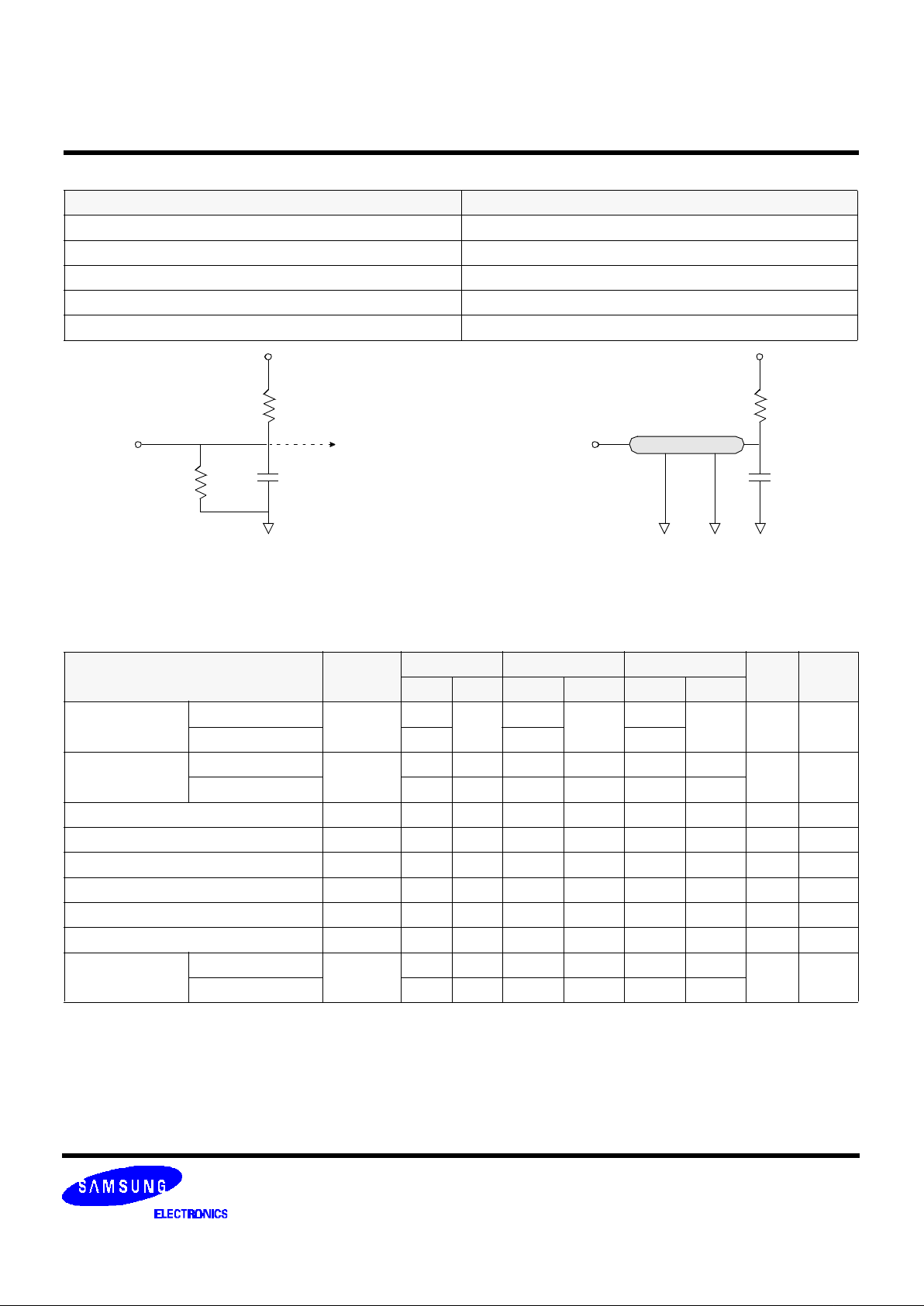
DECOUPLING CAPACITANCE GUIDE LINE
Recommended decoupling capacitance added to power line at board.
Parameter Symbol Value Unit
Decoupling Capacitance between VDD and VSS CDC1 0.1 + 0.01 uF
Decoupling Capacitance between VDDQ and VSSQ CDC2 0.1 + 0.01 uF
1. VDD and VDDQ pins are separated each other.
All VDD pins are connected in chip. All VDDQ pins are connected in chip.
2. VSS and VSSQ pins are separated each other
All VSS pins are connected in chip. All VSSQ pins are connected in chip.
Note :
ABSOLUTE MAXIMUM RATINGS(Voltage referenced to VSS)
Parameter Symbol Value Unit
Voltage on any pin relative to Vss VIN, VOUT -1.0 ~ 4.6 V
Voltage on VDD supply relative to Vss VDD, VDDQ -1.0 ~ 4.6 V
Storage temperature TSTG -55 ~ +150 °C
Power dissipation PD 1 W
Short circuit current IOS 50 mA
Permanent device damage may occur if "ABSOLUTE MAXIMUM RATINGS" are exceeded.
Functional operation should be restricted to recommended operating condition.
Exposure to higher than recommended voltage for extended periods of time could affect device reliability.
Note :
DC OPERATING CONDITIONS
Recommended operating conditions (Voltage referenced to VSS = 0V)
Parameter Symbol Min Typ Max Unit Note
Supply voltage VDD, VDDQ 3.0 3.3 3.6 V
Input high voltage VIH 2.0 3.0 VDD+0.3 V
Input low voltage VIL -0.3 0 0.8 V Note 1
Output high voltage VOH 2.4 - - V IOH = -2mA
Output low voltage VOL - - 0.4 V IOL = 2mA
Input leakage current IIL -5 - 5 uA Note 2
Output leakage current IOL -5 - 5
uA
Note 3
Output Loading Condition see figure 1
1. VIL (min) = -1.5V AC(pulse width ≤ 5ns).
2. Any input 0V ≤ VIN ≤ VDD + 0.3V, all other pins are not under test = 0V.
3. Dout is disabled, 0V ≤ VOUT ≤ VDD.
Note :
CAPACITANCE (VDD/VDDQ = 3.3V, TA = 25°C, f = 1MHz)
Parameter Symbol Min Max Unit
Input capacitance (A0 ~ A9) CIN1 - 4 pF
Input capacitance
(CLK, CKE, CS, RAS, CAS, WE, DSF & DQM)
CIN2 - 4 pF
Data input/output capacitance (DQ0 ~ DQ31) COUT - 5 pF
KM4132G271B CMOS SGRAM
- 7 -
Rev. 2.4 (May 1998)
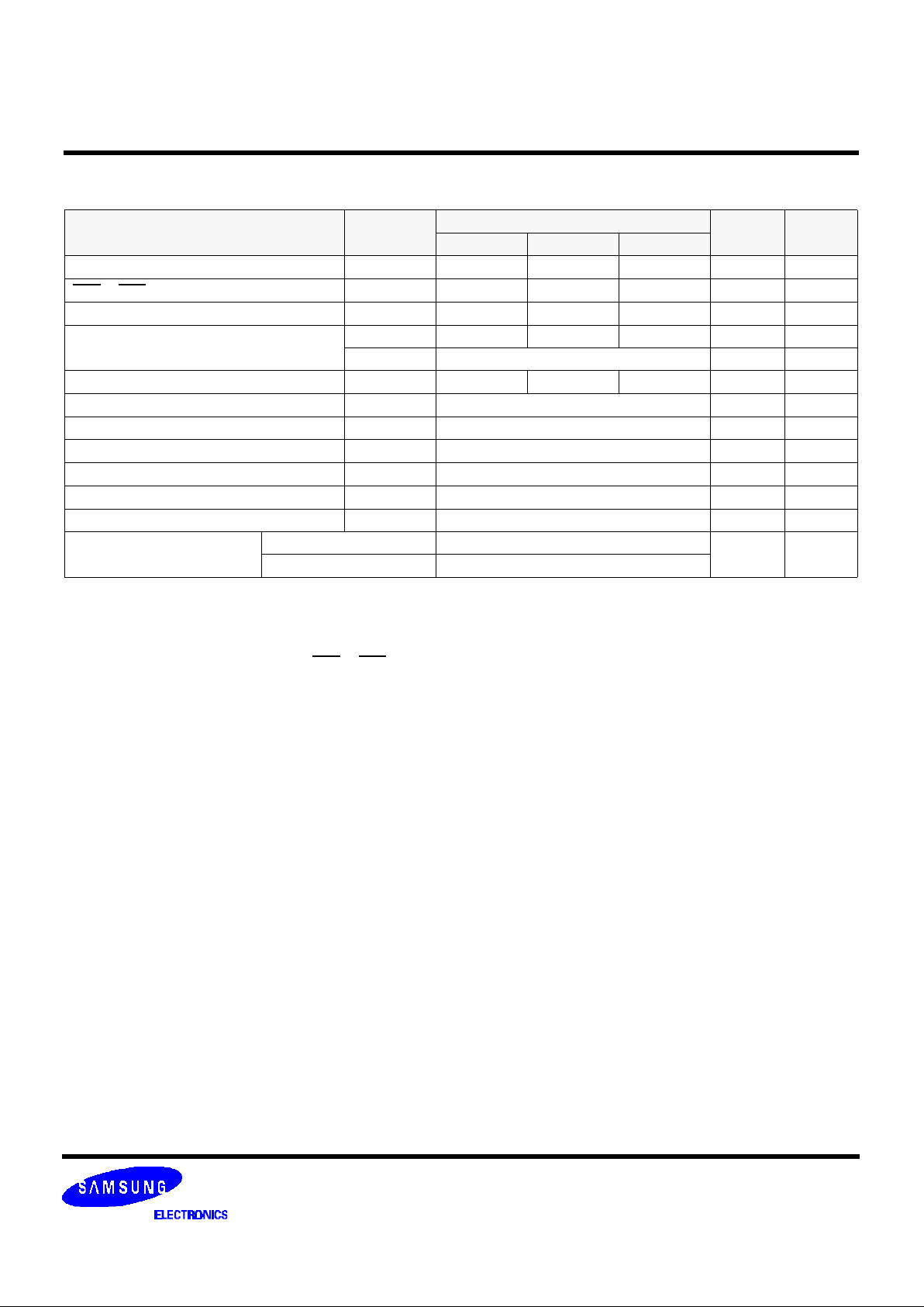
DC CHARACTERISTICS
(Recommended operating condition unless otherwise noted, TA = 0 to 70°C VIH(min) /VIL(max) =2.0V/0.8V)
Parameter Symbol Test Condition
CAS
Latency
Speed
Unit Note
-7 -8 -10
Operating Current
(One Bank Active)
ICC1
Burst Length =1
tRC ≥ tRC(min), tCC ≥ tCC(min), IOL = 0 mA
180 160 150 mA 1
Precharge Standby Current
in power-down mode
ICC2P CKE ≤ VIL(max), tCC = 15ns 2
mA
ICC2PS CKE ≤ VIL(max), CLK ≤ VIL(max), tCC = ∞ 2
Precharge Standby Current
in non power-down mode
ICC2N
CKE ≥ VIH(min), CS ≥ VIH(min), tCC = 15ns
Input signals are changed one time during 30ns
35
mA
ICC2NS
CKE ≥ VIH(min), CLK ≤ VIL(max), tCC = ∞
Input signals are stable
15
Active Standby Current
in power-down mode
ICC3P CKE ≤ VIL(max), tCC = 15ns 3
mA
ICC3PS CKE ≤ VIL(max), CLK ≤ VIL(max), tCC = ∞ 3
Active Standby Current
in non power-down mode
(One Bank Active)
ICC3N
CKE ≥ VIH(min), CS ≥ VIH(min), tCC = 15ns
Input signals are changed one time during 30ns
50
mA
ICC3NS
CKE ≥ VIH(min), CLK ≤ VIL(max), tCC = ∞
Input signals are stable
25
Operating Current
(Burst Mode)
ICC4
IOL = 0 mA, Page Burst
All bank Activated, tCCD = tCCD (min)
3 300 280 210
mA 1
2 180 180 160
Refresh Current ICC5 tRC ≥ tRC(min) 90 90 90 mA 2
Self Refresh Current ICC6 CKE ≤ 0.2V 2 mA
Operating Current
(One Bank Block Write)
ICC7 tCC ≥ tCC(min), IOL=0mA, tBWC (min) 210 190 150 mA
Note :
1. Measured with outputs open. Addresses are changed only one time during tcc(min).
2. Refresh period is 32ms. Addresses are changed only one time during tcc(min).
KM4132G271B CMOS SGRAM
- 8 -
Rev. 2.4 (May 1998)
AC OPERATING TEST CONDITIONS (VDD = 3.3V±0.3V, TA = 0 to 70°C)
Parameter Value
AC input levels Vih/Vil = 2.4V / 0.4V
Input timing measurement reference level 1.4V
Input rise and fall time(See note 3)
tR/tF=1ns/ 1ns
Output timing measurement reference level 1.4V
Output load condition See Fig. 2
3.3V
1200Ω
870Ω
Output
30pF
VOH (DC) = 2.4V, IOH = -2mA
VOL (DC) = 0.4V, IOL = 2mA
Vtt = 1.4V
50Ω
Output
30pF
Z0=50Ω
(Fig. 2) AC Output Load Circuit (Fig. 1) DC Output Load Circuit
1. Parameters depend on programmed CAS latency.
2. If clock rising time is longer than 1ns, (tr/2-0.5)ns should be added to the parameter.
3. Assumed input rise and fall time (tr & tf)=1ns.
If tr & tf is longer than 1ns, transient time compensation should be considered,
i.e., [(tr + tf)/2-1]ns should be added to the parameter.
Note :
•
•
•
•
AC CHARACTERISTICS (AC operating conditions unless otherwise noted)
* All AC parameters are measured from half to half.
Parameter Symbol
-7 -8 -10
Unit Note
Min Max Min Max Min Max
CLK cycle time
CAS Latency=3
tCC
7
1000
8
1000
10
1000 ns 1
CAS Latency=2 12 12 13
CLK to valid
output delay
CAS Latency=3
tSAC
- 6 - 6.5 - 7
ns 1, 2
CAS Latency=2 - 8 - 8 - 9
Output data hold time tOH 2.5 2.5 2.5 ns 2
CLK high pulse width tCH 2.5 3 3.5 ns 3
CLK low pulse width tCL 2.5 3 3.5 ns 3
Input setup time tSS 2 2.5 2.5 ns 3
Input hold time tSH 1 1 1 ns 3
CLK to output in Low-Z tSLZ 1 1 1 ns 2
CLK to output
in Hi-Z
CAS latency=3
tSHZ
- 6 - 6.5 - 7
ns
CAS latency=2 - 8 - 8 - 9
KM4132G271B CMOS SGRAM
- 9 -
Rev. 2.4 (May 1998)
OPERATING AC PARAMETER
1. The minimum number of clock cycles is determined by dividing the minimum time required with clock cycle time and then
rounding off to the next higher integer.
2. Minimum delay is required to complete write.
3. This parameter means minimum CAS to CAS delay at block write cycle only.
4. In case of row precharge interrupt, auto precharge and read burst stop.
Note :
(AC operating conditions unless otherwise noted)
Parameter Symbol
Version
Unit Note
-7 -8 -10
Row active to row active delay tRRD(min) 14 16 20 ns 1
RAS to CAS delay tRCD(min) 16 16 20 ns 1
Row precharge time tRP(min) 21 20 20 ns 1
Row active time
tRAS(min) 49 48 50 ns 1
tRAS(max) 100 us
Row cycle time tRC(min) 70 70 70 ns 1
Last data in to new col. address delay tCDL(min) 1 CLK 2
Last data in to row precharge tRDL(min) 1 CLK 2
Last data in to burst stop tBDL(min) 1 CLK 2
Col. address to col. address delay tCCD(min) 1 CLK 3
Block write data-in to PRE command delay tBPL(min) 1 CLK
Block write cycle time tBWC(min) 1 CLK 1, 3
Number of valid output data
CAS latency=3 2
CLK 4
CAS latency=2 1
KM4132G271B CMOS SGRAM
- 10
Rev. 2.4 (May 1998)
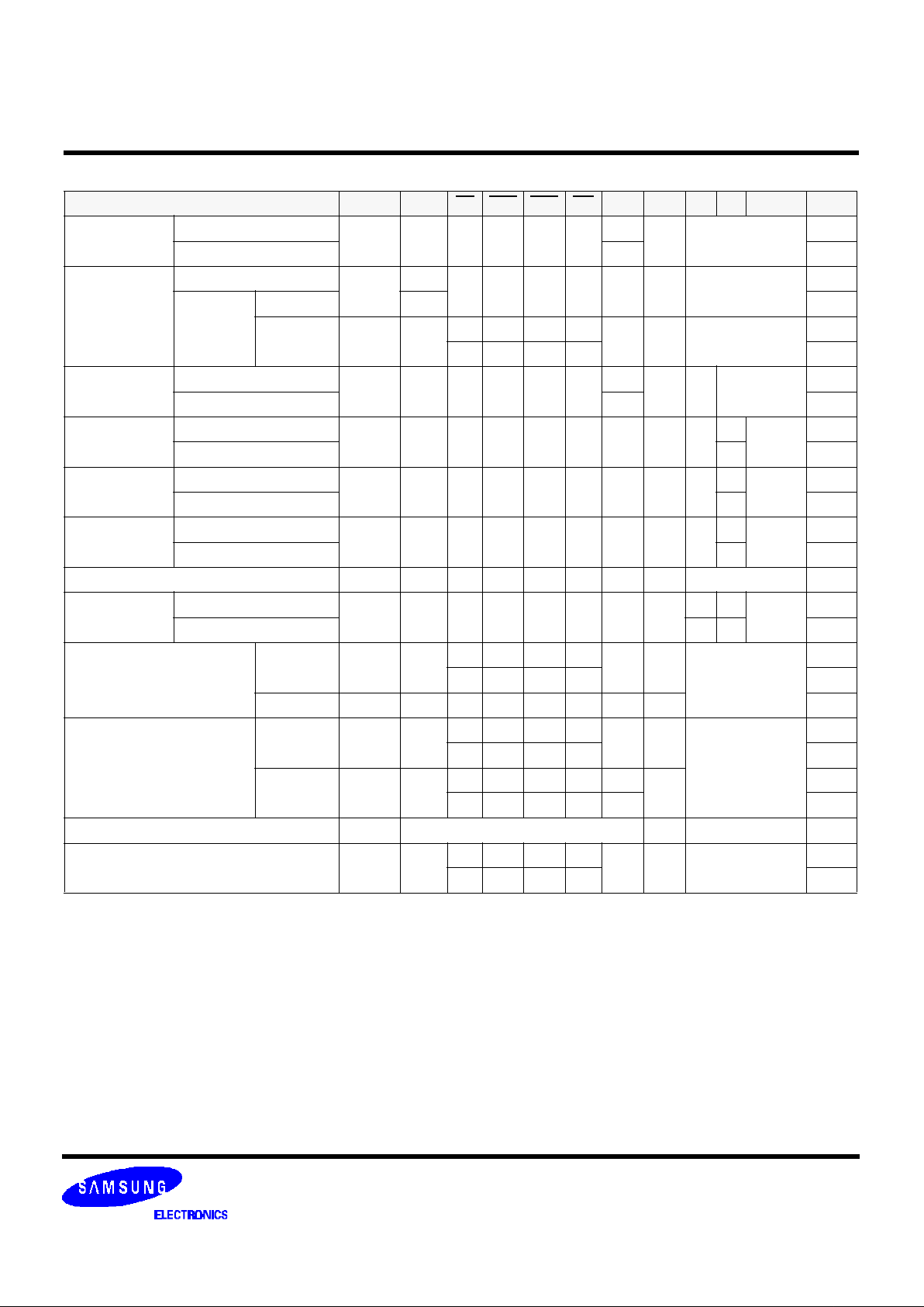
SIMPLIFIED TRUTH TABLE
(V=Valid, X=Don′t Care, H=Logic High, L=Logic Low)
COMMAND CKEn-1 CKEn CS RAS CAS WE DSF DQM A9 A8 A7~ A0 Note
Register Mode Register Set
H X L L L L
L
X OP CODE
1, 2
Special Mode Register Set H 1,2,7
Refresh Auto Refresh
H
H
L L L H L X X
3
Self
Refresh
Entry L 3
Exit L H
L H H H
X X X
3
H X X X 3
Bank Active
& Row Addr.
Write Per Bit Disable
H X L L H H
L
X V Row Address
4, 5
Write Per Bit Enable H 4,5,9
Read &
Column Address
Auto Precharge Disable
H X L H L H L X V
L Column
Address
4
Auto Precharge Enable H 4, 6
Write &
Column Address
Auto Precharge Disable
H X L H L L L X V
L Column
Address
4, 5
Auto Precharge Enable H 4,5,6,9
Block Write &
Column Addr.
Auto Precharge Disable
H X L H L L H X V
L Column
Address
4, 5
Auto Precharge Enable H 4,5,6,9
Burst Stop H X L H H L L X X 7
Precharge
Bank Selection
H X L L H L L X
V L
X
Both Banks X H
Clock Suspend or
Active Power Down
Entry H L
L H H H
X X
X
H X X X
Exit L H X X X X X X
Precharge Power Down Mode
Entry H L
L H H H
X X
X
H X X X
Exit L H
L V V V V
X
H X X X X
DQM H X V X 8
No Operation Command H X
L H H H
X X X
H X X X
1. OP Code : Operand Code
A0 ~ A9 : Program keys. (@MRS)
A5, A6 : LMR or LCR select. (@SMRS)
Color register exists only one per DQi which both banks share.
So dose Mask Register.
Color or mask is loaded into chip through DQ pin.
2. MRS can be issued only at both banks precharge state.
SMRS can be issued only if DQ′s are idle.
A new command can be issued at the next clock of MRS/SMRS.
Note :
KM4132G271B CMOS SGRAM
- 11
Rev. 2.4 (May 1998)
SGRAM vs SDRAM
If DSF is low, SGRAM functionality is identical to SDRAM functionality .
SGRAM can be used as an unified memory by the appropriate DSF control
--> SGRAM=Graphic Memory + Main Memory
Function MRS Bank Active Write
DSF L H L H L H
SGRAM
Function
MRS SMRS
Bank Active
with
Write per bit
Disable
Bank Active
with
Write per bit
Enable
Normal
Write
Block
Write
3. Auto refresh functions as same as CBR refresh of DRAM.
The automatical precharge without Row precharge command is meant by "Auto".
Auto/Self refresh can be issued only at both precharge state.
4. A9 : Bank select address.
If "Low" at read, (block) write, Row active and precharge, bank A is selected.
If "High" at read, (block) write, Row active and precharge, bank B is selected.
If A8 is "High" at Row precharge, A9 is ignored and both banks are selected.
5. It is determined at Row active cycle.
whether Normal/Block write operates in write per bit mode or not.
For A bank write, at A bank Row active, for B bank write, at B bank Row active.
Terminology : Write per bit =I/O mask
(Block) Write with write per bit mode=Masked(Block) Write
6. During burst read or write with auto precharge, new read/(block) write command cannot be issued.
Another bank read/(block) write command can be issued at tRP after the end of burst.
7. Burst stop command is valid only at full page burst length.
8. DQM sampled at positive going edge of a CLK.
masks the data-in at the very CLK(Write DQM latency is 0)
but makes Hi-Z state the data-out of 2 CLK cycles after.(Read DQM latency is 2)
9. Graphic features added to SDRAM′s original features.
If DSF is tied to low, graphic functions are disabled and chip operates as a 8M SDRAM with 32 DQ′s.
SIMPLIFIED TRUTH TABLE
KM4132G271B CMOS SGRAM
- 12
Rev. 2.4 (May 1998)
MODE REGISTER FIELD TABLE TO PROGRAM MODES
POWER UP SEQUENCE
1. Apply power and start clock, Attempt to maintain CKE= "H", DQM= "H" and the other pins are NOP condition at the inputs.
2. Maintain stable power, stable clock and NOP input condition for a minimum of 200us.
3. Issue precharge commands for all banks of the devices.
4. Issue 2 or more auto-refresh commands.
5. Issue a mode register set command to initialize the mode register.
cf.) Sequence of 4 & 5 may be changed.
The device is now ready for normal operation.
Note : 1. If A9 is high during MRS cycle, "Burst Read Single Bit Write" function will be enabled.
2. The full column burst(256bit) is available only at Sequential mode of burst type.
3. If LC and LM both high(1), data of mask and color register will be unknown.
Register Programmed with MRS
(Note 1)
Address A9 A8 A7 A6 A5 A4 A3 A2 A1 A0
Function W.B.L TM CAS Latency BT Burst Length
(Note 2)
Test Mode CAS Latency Burst Type Burst Length
A8 A7 Type A6 A5 A4 Latency A3 Type A2 A1 A0 BT=0 BT=1
0 0 Mode Register Set 0 0 0 Reserved 0 Sequential 0 0 0 1 Reserved
0 1 Vendor
Use
Only
0 0 1 - 1 Interleave 0 0 1 2 Reserved
1 0 0 1 0 2 0 1 0 4 4
1 1 0 1 1 3 0 1 1 8 8
Write Burst Length 1 0 0 Reserved 1 0 0 Reserved Reserved
A9 Length 1 0 1 Reserved 1 0 1 Reserved Reserved
0 Burst 1 1 0 Reserved 1 1 0 Reserved Reserved
1 Single Bit 1 1 1 Reserved 1 1 1 256(Full) Reserved
Special Mode Register Programmed with SMRS
Address A9 A8 A7 A6 A5 A4 A3 A2 A1 A0
Function X LC LM X
(Note 3)
Load Color Load Mask
A6 Function A5 Function
0 Disable 0 Disable
1 Enable 1 Enable
KM4132G271B CMOS SGRAM
- 13
Rev. 2.4 (May 1998)
BURST SEQUENCE (BURST LENGTH = 4)
Initial address
Sequential Interleave
A1 A0
0 0 0 1 2 3 0 1 2 3
0 1 1 2 3 0 1 0 3 2
1 0 2 3 0 1 2 3 0 1
1 1 3 0 1 2 3 2 1 0
BURST SEQUENCE (BURST LENGTH = 8)
Initial address
Sequential Interleave
A2 A1 A0
0 0 0 0 1 2 3 4 5 6 7 0 1 2 3 4 5 6 7
0 0 1 1 2 3 4 5 6 7 0 1 0 3 2 5 4 7 6
0 1 0 2 3 4 5 6 7 0 1 2 3 0 1 6 7 4 5
0 1 1 3 4 5 6 7 0 1 2 3 2 1 0 7 6 5 4
1 0 0 4 5 6 7 0 1 2 3 4 5 6 7 0 1 2 3
1 0 1 5 6 7 0 1 2 3 4 5 4 7 6 1 0 3 2
1 1 0 6 7 0 1 2 3 4 5 6 7 4 5 2 3 0 1
1 1 1 7 0 1 2 3 4 5 6 7 6 5 4 3 2 1 0
PIXEL to DQ MAPPING(at BLOCK WRITE)
Column address 3 Byte 2 Byte 1 Byte 0 Byte
A2 A1 A0 I/O31 - I/O24 I/O23 - I/O 16 I/O15 - I/O8 I/O7 - I/O0
0 0 0 DQ24 DQ16 DQ8 DQ0
0 0 1 DQ25 DQ17 DQ9 DQ1
0 1 0 DQ26 DQ18 DQ10 DQ2
0 1 1 DQ27 DQ19 DQ11 DQ3
1 0 0 DQ28 DQ20 DQ12 DQ4
1 0 1 DQ29 DQ21 DQ13 DQ5
1 1 0 DQ30 DQ22 DQ14 DQ6
1 1 1 DQ31 DQ23 DQ15 DQ7
KM4132G271B CMOS SGRAM
- 14
Rev. 2.4 (May 1998)
CLOCK (CLK)
The clock input is used as the reference for all SGRAM operations. All operations are synchronized to the positive going edge
of the clock. The clock transitions must be monotonic between
VIL and VIH. During operation with CKE high all inputs are
assumed to be in a valid state (low or high) for the duration of
set-up and hold time around positive edge of the clock for proper
functionality and ICC specifications.
CLOCK ENABLE (CKE)
The clock enable(CKE) gates the clock onto SGRAM. If CKE
goes low synchronously with clock (set-up and hold time are the
same as other inputs), the internal clock is suspended from the
next clock cycle and the state of output and burst address is frozen as long as the CKE remains low. All other inputs are ignored
from the next clock cycle after CKE goes low. When both banks
are in the idle state and CKE goes low synchronously with clock,
the SGRAM enters the power down mode from the next clock
cycle. The SGRAM remains in the power down mode ignoring
the other inputs as long as CKE remains low. The power down
exit is synchronous as the internal clock is suspended. When
CKE goes high at least "tSS + 1CLOCK " before the high going
edge of the clock, then the SGRAM becomes active from the
same clock edge accepting all the input commands.
BANK SELECT (A9)
This SGRAM is organized as two independent banks of 131,072
words x 32 bits memory arrays. The A9 inputs is latched at the
time of assertion of RAS and CAS to select the bank to be used
for the operation. When A9 is asserted low, bank A is selected.
When A9 is asserted high, bank B is selected. The bank select
A9 is latched at bank activate, read, write mode register set and
precharge operations.
ADDRESS INPUT (A0 ~ A8)
The 17 address bits required to decode the 131,072 word locations are multiplexed into 9 address input pins(A0~A8). The 9 bit
row address is latched along with RAS and A9 during bank acti-
vate command. The 8 bit column address is latched along with
CAS, WE and A9 during read or write command.
NOP and DEVICE DESELECT
When RAS, CAS and WE are high, the SGRAM performs no
operation (NOP). NOP does not initiate any new operation, but
is needed to complete operations which require more than single clock cycle like bank activate, burst read, auto refresh, etc.
The device deselect is also a NOP and is entered by asserting
CS high. CS high disables the command decoder so that RAS,
CAS, WE, DSF and all the address inputs are ignored.
DEVICE OPERATIONS
POWER-UP
The following sequence is recommended for POWER UP
MODE REGISTER SET (MRS)
The mode register stores the data for controlling the various
operating modes of SGRAM. It programs the CAS latency,
addressing mode, burst length, test mode and various vendor
specific options to make SGRAM useful for variety of different
applications. The default value of the mode register is not
defined, therefore the mode register must be written after power
up to operate the SGRAM. The mode register is written by
asserting low on CS, RAS, CAS, WE and DSF (The SGRAM
should be in active mode with CKE already high prior to writing
the mode register). The state of address pins A0 ~ A8 and A9 in
the same cycle as CS, RAS, CAS, WE and DSF going low is the
data written in the mode register. One clock cycle is required to
complete the write in the mode register. The mode register contents can be changed using the same command and clock cycle
requirements during operation as long as both banks are in the
idle state. The mode register is divided into various fields
depending on functionality. The burst length field uses A0 ~ A2,
burst type uses A3, addressing mode uses A4 ~ A6, A7 ~ A8 are
used for vendor specific options or test mode. And the write
burst length is programmed using A9. A7 ~ A8 must be set to low
for normal SGRAM operation. Refer to table for specific codes
for various burst length, addressing modes and CAS latencies.
Power must be applied to either CKE and DQM inputs to pull
them high and other pins are NOP condition at the inputs
before or along with V DD(and VDDQ ) supply.
The clock signal must also be asserted at the same time.
After VDD reaches the desired voltage, a minimum pause of
200 microseconds is required with inputs in NOP condition.
Both banks must be precharged now.
Perform a minimum of 2 Auto refresh cycles to stabilize the
internal circuitry.
Perform a MODE REGISTER SET cycle to program the CAS
latency, burst length and burst type as the default value of
mode register is undefined.
At the end of one clock cycle from the mode register set
cycle, the device is ready for operation.
When the above sequence is used for Power-up, all the outputs will be in high impedance state. The high impedance of
outputs is not guaranteed in any other power-up sequence.
cf.) Sequence of 4 & 5 may be changed.
1.
2.
3.
4.
5.

KM4132G271B CMOS SGRAM
- 15
Rev. 2.4 (May 1998)
BANK ACTIVATE
The bank activate command is used to select a random row in
an idle bank. By asserting low on RAS and CS with desired row
and bank addresses, a row access is initiated. The read or write
operation can occur after a time delay of tRCD(min) from the time
of bank activation. tRCD(min) is an internal timing parameter of
SGRAM, therefore it is dependent on operating clock frequency.
The minimum number of clock cycles required between bank
activate and read or write command should be calculated by
dividing tRCD(min) with cycle time of the clock and then rounding
off the result to the next higher integer. The SGRAM has two
internal banks on the same chip and shares part of the internal
circuitry to reduce chip area, therefore it restricts the activation
of both banks immediately. Also the noise generated during
sensing of each bank of SGRAM is high requiring some time for
power supplies to recover before the other bank can be sensed
reliably. tRRD(min) specifies the minimum time required between
activating different banks. The number of clock cycles required
between different bank activation must be calculated similar to
tRCD specification. The minimum time required for the bank to be
active to initiate sensing and restoring the complete row of
dynamic cells is determined by tRAS(min) specification before a
precharge command to that active bank can be asserted. The
maximum time any bank can be in the active state is determined
by tRAS(max). The number of cycles for both tRAS(min) and
tRAS(max) can be calculated similar to tRCD specification.
BURST READ
The burst read command is used to access burst of data on consecutive clock cycles from an active row in an active bank. The
burst read command is issued by asserting low on CS and CAS
with WE being high on the positive edge of the clock. The bank
must be active for at least tRCD(min) before the burst read com-
mand is issued. The first output appears CAS latency number of
clock cycles after the issue of burst read command. The burst
length, burst sequence and latency from the burst read command is determined by the mode register which is already programmed. The burst read can be initiated on any column
address of the active row. The address wraps around if the initial
address does not start from a boundary such that number of outputs from each I/O are equal to the burst length programmed in
the mode register. The output goes into high-impedance at the
end of the burst, unless a new burst read was initiated to keep
the data output gapless. The burst read can be terminated by
issuing another burst read or burst write in the same bank or the
other active bank or a precharge command to the same bank.
The burst stop command is valid only at full page burst length
where the output does not go into high impedance at the end of
burst and the burst is wrapped around..
BURST WRITE
The burst write command is similar to burst read command, and
is used to write data into the SGRAM on consecutive clock
DEVICE OPERATIONS
cycles in adjacent addresses depending on burst length and
burst sequence. By asserting low on CS, CAS and WE with valid
column address, a write burst is initiated. The data inputs are
provided for the initial address in the same clock cycle as the
burst write command. The input buffer is deselected at the end
of the burst length, even though the internal writing may not
have been completed yet. The writing can not complete to burst
length. The burst write can be terminated by issuing a burst
read and DQM for blocking data inputs or burst write in the same
or the other active bank. The burst stop command is valid only at
full page burst length where the writing continues at the end of
burst and the burst is wrapped around. The write burst can also
be terminated by using DQM for blocking data and precharging
the bank " tRDL" after the last data input to be written into the
active row. See DQM OPERATION also.
DQM OPERATION
The DQM is used to mask input and output operations. It works
similar to OE during read operation and inhibits writing during
write operation. The read latency is two cycles from DQM and
zero cycle for write, which means DQM masking occurs two
cycles later in the read cycle and occurs in the same cycle during write cycle. DQM operation is synchronous with the clock,
therefore the masking occurs for a complete cycle. The DQM
signal is important during burst interrupts of write with read or
precharge in the SGRAM. Due to asynchronous nature of the
internal write, the DQM operation is critical to avoid unwanted or
incomplete writes when the complete burst write is not required.
DQM is also used for device selection, byte selection and bus
control in a memory system. DQM0 controls DQ0 to DQ7,
DQM1 controls DQ8 to DQ15, DQM2 controls DQ16 to DQ23,
DQM3 controls DQ24 to DQ31. DQM masks the DQ′s by a byte
regardless that the corresponding DQ′s are in a state of WPB
masking or Pixel masking. Please refer to DQM timing diagram
also.
PRECHARGE
The precharge operation is performed on an active bank by
asserting low on CS, RAS, WE and A8 with valid A9 of the bank
to be precharged. The precharge command can be asserted
anytime after tRAS(min) is satisfied from the bank activate command in the desired bank. "tRP" is defined as the minimum time
required to precharge a bank. The minimum number of clock
cycles required to complete row precharge is calculated by
dividing "tRP" with clock cycle time and rounding up to the next
higher integer. Care should be taken to make sure that burst
write is completed or DQM is used to inhibit writing before precharge command is asserted. The maximum time any bank can
be active is specified by tRAS(max). Therefore, each bank has to
be precharged within tRAS(max) from the bank activate com-
mand. At the end of precharge, the bank enters the idle state
and is ready to be activated again.
KM4132G271B CMOS SGRAM
- 16
Rev. 2.4 (May 1998)
Entry to Power Down, Auto refresh, Self refresh and Mode register Set etc. is possible only when both banks are in idle state.
AUTO PRECHARGE
The precharge operation can also be performed by using auto
precharge. The SGRAM internally generates the timing to satisfy
tRAS(min) and "tRP" for the programmed burst length and CAS
latency. The auto precharge command is issued at the same
time as burst read or burst write by asserting high on A8. If burst
read or burst write command is issued with low on A8, the bank
is left active until a new command is asserted. Once auto precharge command is given, no new commands are possible to
that particular bank until the bank achieves idle state.
BOTH BANKS PRECHARGE
Both banks can be precharged at the same time by using Pre-
charge all command. Asserting low on CS, RAS, and WE with
high on A8 after both banks have satisfied tRAS (min) require-
ment, performs precharge on both banks. At the end of tRP after
performing precharge all, both banks are in idle state.
AUTO REFRESH
The storage cells of SGRAM need to be refreshed every 16ms
to maintain data. An auto refresh cycle accomplishes refresh of
a single row of storage cells. The internal counter increments
automatically on every auto refresh cycle to refresh all the rows.
An auto refresh command is issued by asserting low on CS,RAS
and CAS with high on CKE and WE. The auto refresh command
can only be asserted with both banks being in idle state and the
device is not in power down mode (CKE is high in the previous
cycle). The time required to complete the auto refresh operation
is specified by "tRC(min)". The minimum number of clock cycles
required can be calculated by driving "tRC" with clock cycle time
and them rounding up to the next higher integer. The auto
refresh command must be followed by NOP′s until the auto
refresh operation is completed. Both banks will be in the idle
state at the end of auto refresh operation. The auto refresh is the
preferred refresh mode when the SGRAM is being used for normal data transactions. The auto refresh cycle can be performed
once in 15.6us or a burst of 1024 auto refresh cycles once in
16ms.
DEVICE OPERATIONS (Continued)
SELF REFRESH
The self refresh is another refresh mode available in the
SGRAM. The self refresh is the preferred refresh mode for data
retention and low power operation of SGRAM. In self refresh
mode, the SGRAM disables the internal clock and all the input
buffers except CKE. The refresh addressing and timing are
internally generated to reduce power consumption.
The self refresh mode is entered from all banks idle state by
asserting low on CS, RAS, CAS and CKE with high on WE.
Once the self refresh mode is entered, only CKE state being low
matters, all the other inputs including the clock are ignored in
order to remain in the self refresh mode.
The self refresh is exited by restarting the external clock and
then asserting high on CKE. This must be followed by NOP′s
for a minimum time of "tRC" before the SGRAM reaches idle
state to begin normal operation. If the system uses burst auto
refresh during normal operation, it is recommended to use burst
1024 auto refresh cycles immediately after exiting self refresh.
DEFINE SPECIAL FUNCTION(DSF)
The DSF controls the graphic applications of SGRAM. If DSF is
tied to low, SGRAM functions as 128K x 32 x2 Bank SDRAM.
SGRAM can be used as an unified memory by the appropriate
DSF command. All the graphic function modes can be entered
only by setting DSF high when issuing commands which otherwise would be normal SDRAM commands. SDRAM functions
such as RAS Active, Write, and WCBR change to SGRAM functions such as RAS Active with WPB, Block Write and SWCBR
respectively. See the section below for the graphic functions that
DSF controls.
SPECIAL MODE REGISTER SET(SMRS)
There are two kinds of special mode registers in SGRAM.One is
color register and the other is mask register. Those usage will be
explained in the "WRITE PER BIT" and "BLOCK WRITE" sections. When A5 and DSF goes high in the same cycle as CS,
RAS, CAS and WE going low, Load Mask Register(LMR) process is executed and the mask registers are filled with the
masks for associated DQ′s through DQ pins. And when A6 and
DSF goes high in the same cycle as CS, RAS, CAS and WE
going low, Load Color Register(LCR) process is executed and
the color register is filled with color data for associated DQ′s
through the DQ pins. If both A5 and A6 are high at SMRS, data
of mask and color cycle are required to complete the write in the
mask register and the color register at LMR and LCR respectively. A new command can be issued in the next clock of LMR
or LCR. SMRS, compared with MRS, can be issued at the active
state under the condition that DQ′s are idle. As in write opera-
tion, SMRS accepts the data needed through DQ pins. Therefore bus contention must be avoided. The more detailed
materials can be obtained by referring corresponding timing diagram.
 Loading...