

Samsung KA2163 Datasheet
KA2163 I2C BUS NTSC 1 CHIP IC FOR COLOR TV
I2C BUS NTSC 1 CHIP FOR COLOR TV
The KA2163 is a monolithic integrated circuit for VIF,
SIF, chroma and deflection circuit of NTSC color TV.
The KA2163 also provides audio / video switch and
OSD interface. It combines these functions in a 56
SDIP package and the KA2163B also includes I2C bus
control functions for automatically adjustment.
FUNCTIONS
- VIF/SIF
- Video
- Chroma
- Deflection
- OSD interface
- I2C bus circuit
FEATURES
VIF CIRCUIT
- PLL type IF demodulation (bus alignment)
- Adjustment free AFT without tank coil
- RF AGC output (delay point : bus alignment)
- Dual time constant fast AGC
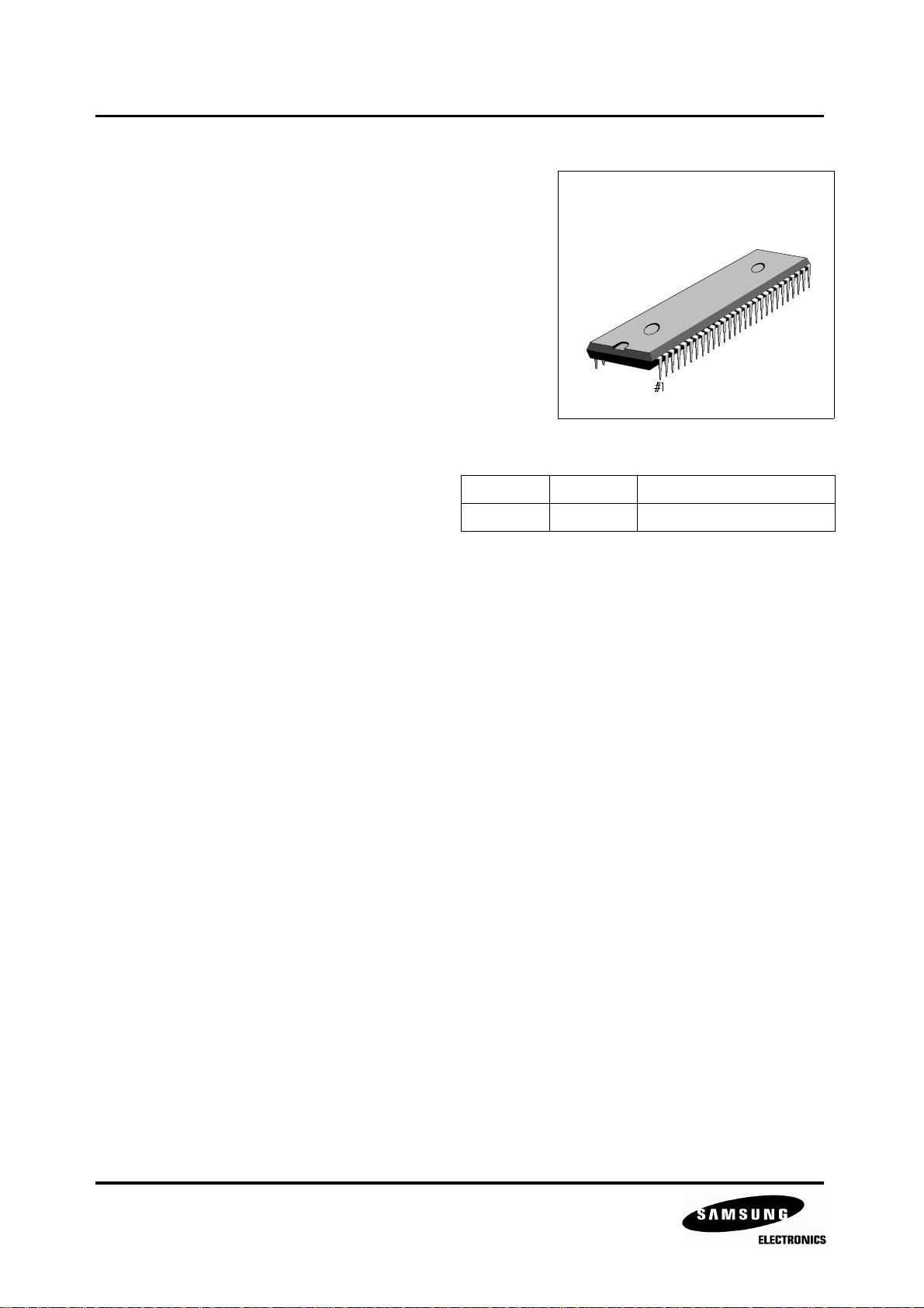
56-SDIP-600
ORDERING INFORMATION
Device Package Operating Temperature
KA2163 56 -SDIP -20¡É ~ +65¡É
OSD CIRCUIT
- Linear RGB input
- Cut off / Drive adjustment (bus adjustment)
- RGB primary color output
SIF CIRCUIT
- Inter carrier SIF system
- External sound select switch (bus select)
- Attenuator circuit
VIDEO CIRCUIT
- Black stretcher
- DC Restoration circuit
- D.L aperture compensate circuit (bus control)
- Internal filter auto-adjust circuit (fsc link type)
- Uni-color circuit(bus control)
- Y delay line circuit
CHROMA CIRCUIT
- Color control circuit (bus control)
- Tint control circuit
DEFLECTION CIRCUIT
- Auto-slicer type high performance
- Sync. separator circuit
- Adjustment free countdown system
- Sync. separation output
- X-ray protect circuit
- Vertical ramp output
- Dual time constant AFC circuit
- Horizontal and Vertical position bus adjustment
- Vertical amplitude adjustment (bus adjustment)
1
M/M-97-D008
97-05-20
KA2163 I2C BUS NTSC 1 CHIP IC FOR COLOR TV
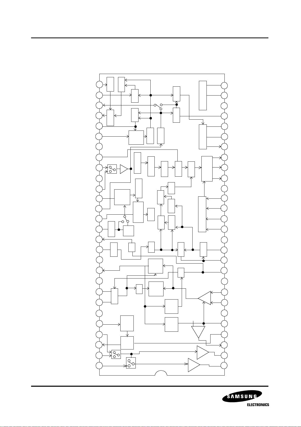
BLOCK DIAGRAM
X-RAY
FBP IN
Sync. OUT
H. OUT
H. AFC
32fHVCO
D. GND
ABL
TV IN
ACL
EXT. VIDEO
BLACK DET
AV/SW OUT
DC REST
Y IN
AFT
CHROMA IN
VCC
TV DET. OUT
SIF VCC
PIF TANK
PIF TANK
SIF GND
LIMITER IN
AUDIO TV IN
29
30
31
32
33
34
35
36
37
38
39
40
41
42
43
44
45
46
47
48
49
50
51
52
53
SDA
X-RAY
H.RAM
AFC-2AFC-1
H. OUT
32fH
VCO
H C / D
H SEPA
X2
Sharpness
Contrast
Smoothing
Black
Streatch
WPS
DC
Restoretion
Clamp
3.58
Trap
BPF
AFT
DEMO
Y-DL
Color
ACC
D
V C /
Bus Interface
V SEPA
V.RAMP
WPL
LPF
TINT
Killer
MTX
Bright
Analogue RGB
APC
VCXO
VCC
I
DET
SW
SIF
VCC
Q
90¡£
VCO
SIF
GND
Limier
DET
LOCK
DET
RF
AGC
AGC
DET
28
SCL
27
H. VCC
26
H.VCC
9.0V
V SEPA FILTER
25
V. RAMP
24
NFB
23
V. OUT
22
B OUT
21
G OUT
20
Cut-off/drive
D.VCC
R OUT
19
D. VCC
18
3.3V
ANALOG B IN
17
ANALOG R IN
16
ANALOG R IN
15
F-BLK
14
GND
13
GND
VCXO
12
APC FILTER
11
LOOP FILTER
10
PIF VCC
9
PIF
VCC
PIF IN
8
PIF IN
7
PIF GND
6
PIF
GND
AGC FILTER
5
SIF TANK
4
DE-EMPHASIS
EXT. AUDIO
EXT. AUDIO
2
54
55
56
FM
DET
M/M-97-D008
ATT
ATT
RF AGC
3
SOUND OUT
2
SOUND OUT
1
97-05-20
KA2163 I2C BUS NTSC 1 CHIP IC FOR COLOR TV
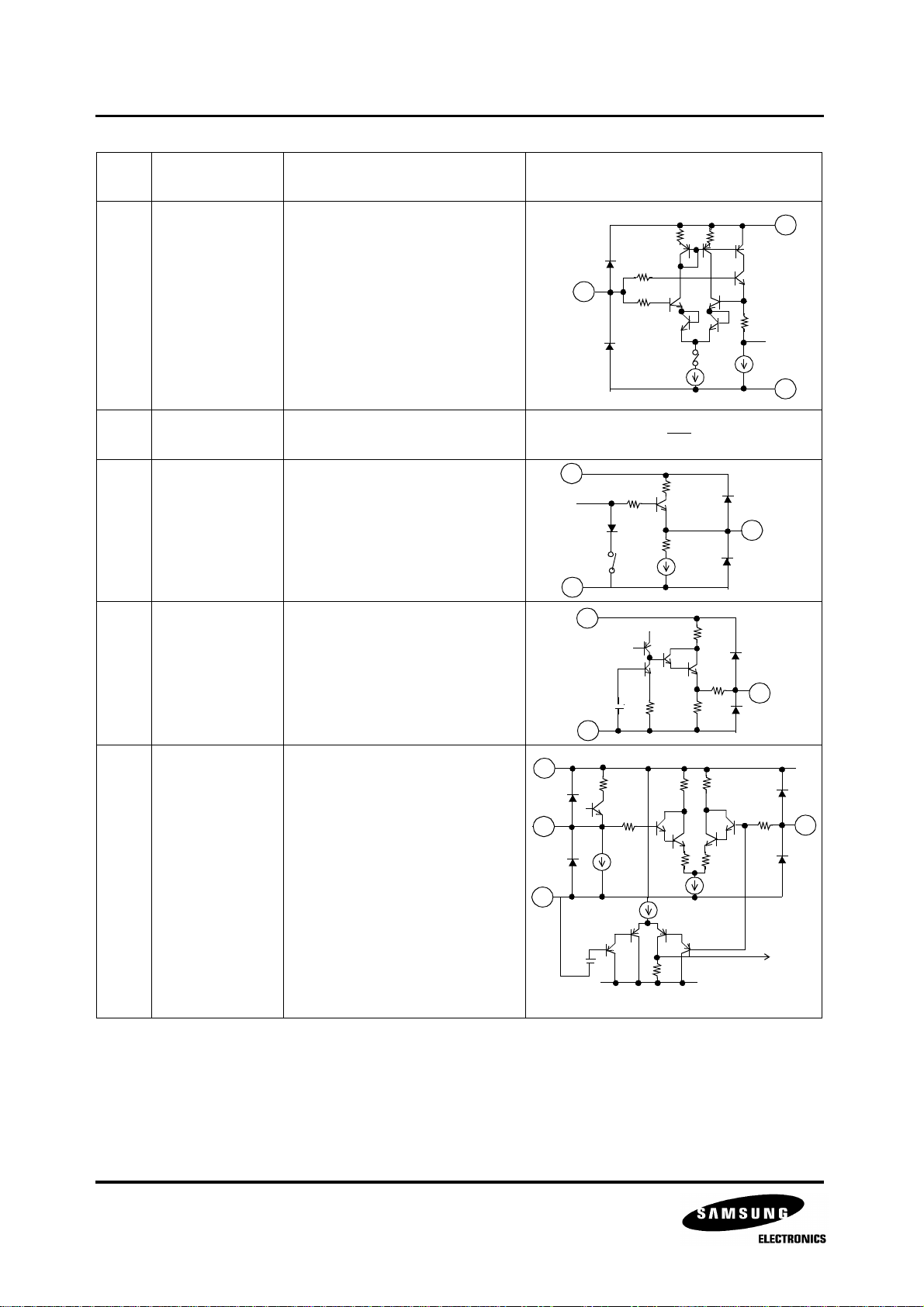
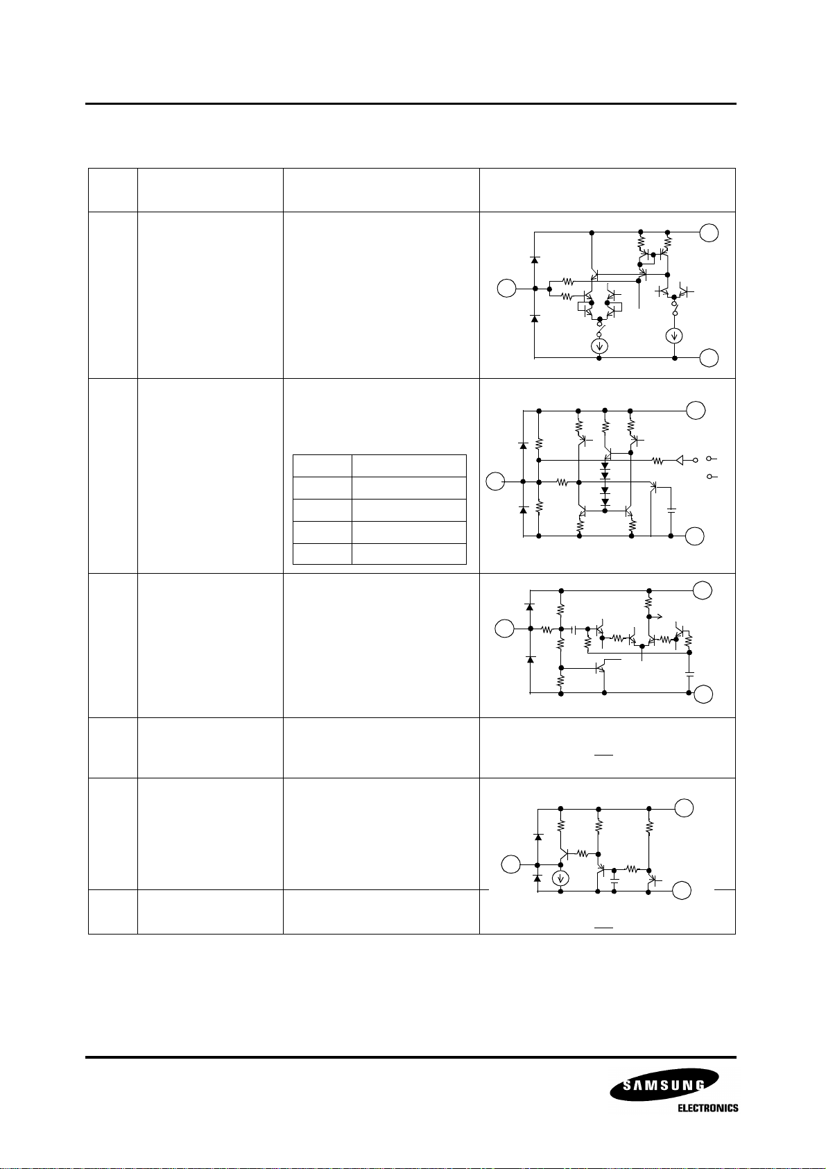
TERMINAL FUNCTION
PIN
PIN NAME FUNCTION INTERFACE CIRCUIT
NO.
1
Sound Output This terminal is for Sound
2
Output.
The maximum flew out
current of these terminals is
3.6mA. So, the minimum load
resister is 1k¥Ø.
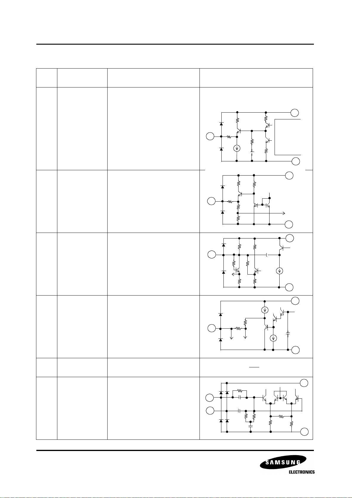
3 RF AGC This terminal is for RF AGC
output.
This terminal is for connecting
SIF detect tank coil.
4 SIF Tank Coil
This terminal is for Sound
Mute Switch, too.
If this terminal is connected to
GND, the sound output is
muted.
48
Attenuator
51
9
Monitor
6
48
500¥ìA
51
34.5k¥
4.5V
30k¥Ø
42¥Ø
3k¥
3k¥Ø
43k¥Ø
5.5PF
500¥
200¥
2
330¥ìA
500¥
300¥
3
30k¥Ø
4
100¥
5 AGC Filter This terminal is for PIF 2nd
AGC filter.
6 PIF GND This terminal is for GND of PIF
circuit.
7
8
PIF Input This terminal is for IF input.
The typical input value is
90dB¥ìV.
3
M/M-97-D008
97-05-20
9
200¥ìA
20k¥Ø
RF AGC
50¥Ø
AGC
Amplifier
100k¥Ø
20pF
20pF
1.2k¥Ø
2V
1.2k¥Ø
50¥ìA
140¥Ø
700¥Ø
100PF
6
9
700¥Ø
6
5
7
8
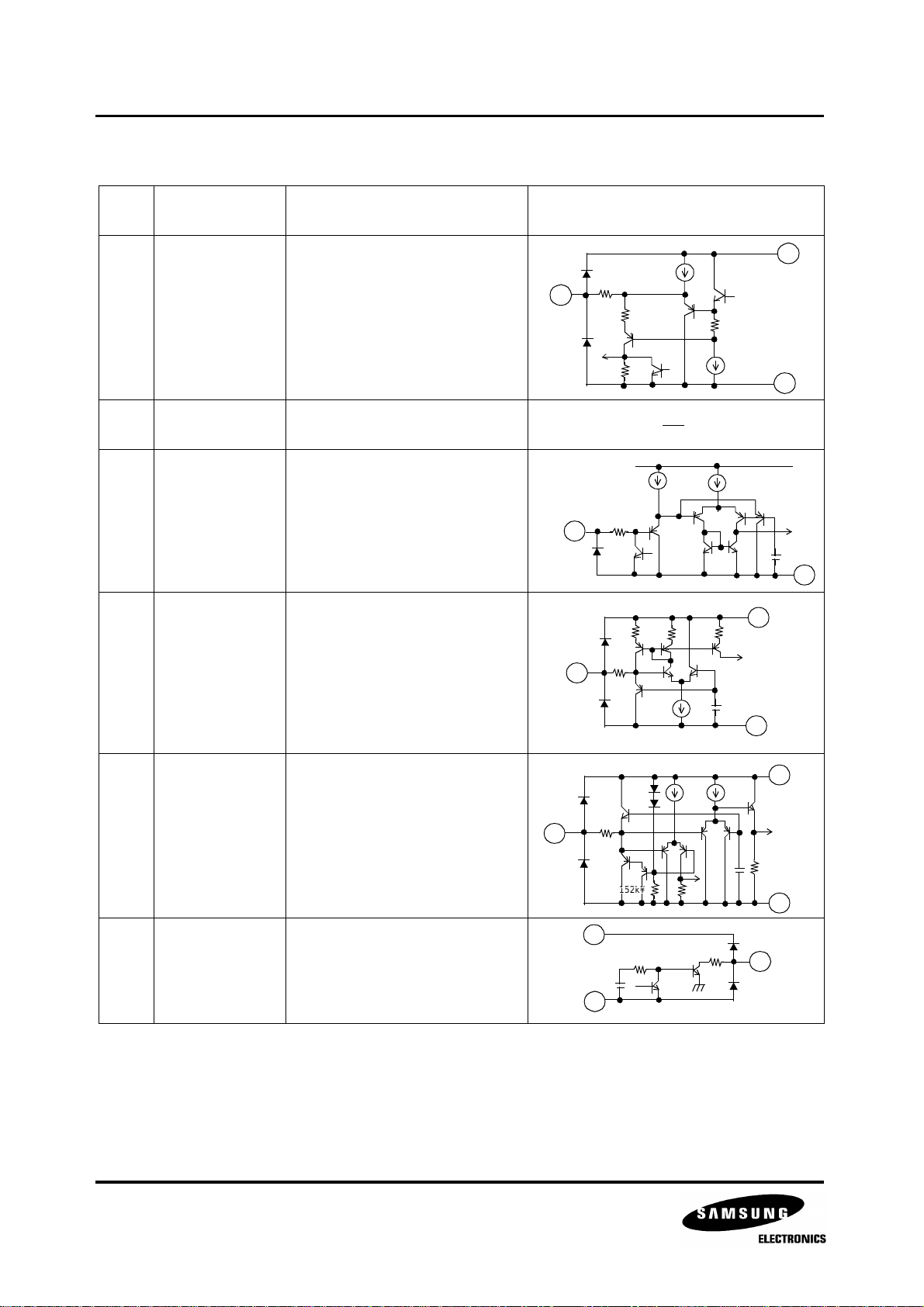
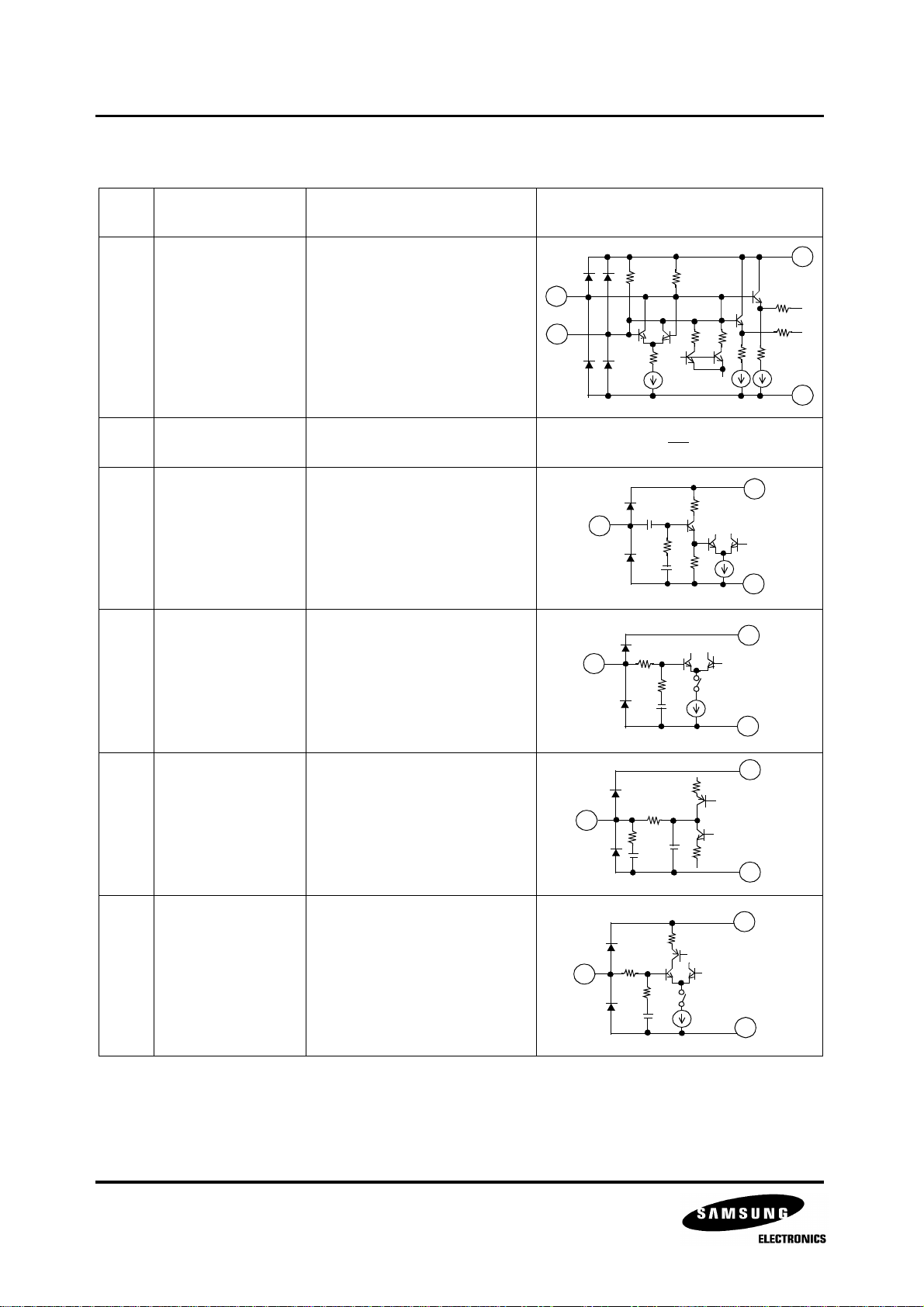
KA2163 I2C BUS NTSC 1 CHIP IC FOR COLOR TV
PIN
PIN NAME FUNCTION INTERFACE CIRCUIT
NO.
9 PIF Vcc This terminal is for Vcc of PIF
circuit.
10 Loop Filter This terminal is for PIF PLL
loop filter.
11 APC Filter This terminal is for APC filter
of fsc oscillation.
11
10
500¥Ø
5k¥Ø
APC Detection
500¥Ø
300¥Ø
300¥Ø
48
51
46
500¥Ø
12 VCXO This terminal is for X’tal of
3.58MHz VCXO.
13 GND This terminal is for V/C/D
GND.
14 Fast Blanking This terminal is for fast
blanking of RGB input.
12
14
7.5¥ìA
800¥Ø
500¥Ø
14k¥Ø
Killer
2.5k¥Ø
2.5k¥Ø
7.5¥ìA
500¥Ø
13
46
2.5k¥Ø
1.5pF
13
46
1V
13
4
M/M-97-D008
97-05-20
KA2163 I2C BUS NTSC 1 CHIP IC FOR COLOR TV
PIN
PIN NAME FUNCTION INTERFACE CIRCUIT
NO.
15
16
Analog RGB
Input
These terminals are for RGB
signal input.
17
18 Digital Vcc This terminal is for Vcc of
digital curcuit.
19
RGB Output This terminal is for RGB
20
primary color signal output.
21
5k¥Ø
15
16
17
46
13
2k¥Ø
400¥Ø
BLK
2k¥Ø
22.5¥ìA
150¥Ø
1mA
5k¥Ø
150¥Ø
46
2k¥Ø
75¥ìA
13
19
20
21
22 Vertical Output This terminal is for vertical
pulse output.
2324NFB, Vertical
Ramp.
These terminals are for NFB
input and vertical ramp
output.
13
46
24
46
13
2.8V
50¥ìA
5k¥Ø
5k¥Ø150¥Ø
1.1k¥Ø
100¥
50¥Ø
10k¥Ø
5k¥Ø
1.1k¥Ø
100¥ìA
RGB Blanking
22
5k¥Ø
13
5
M/M-97-D008
97-05-20
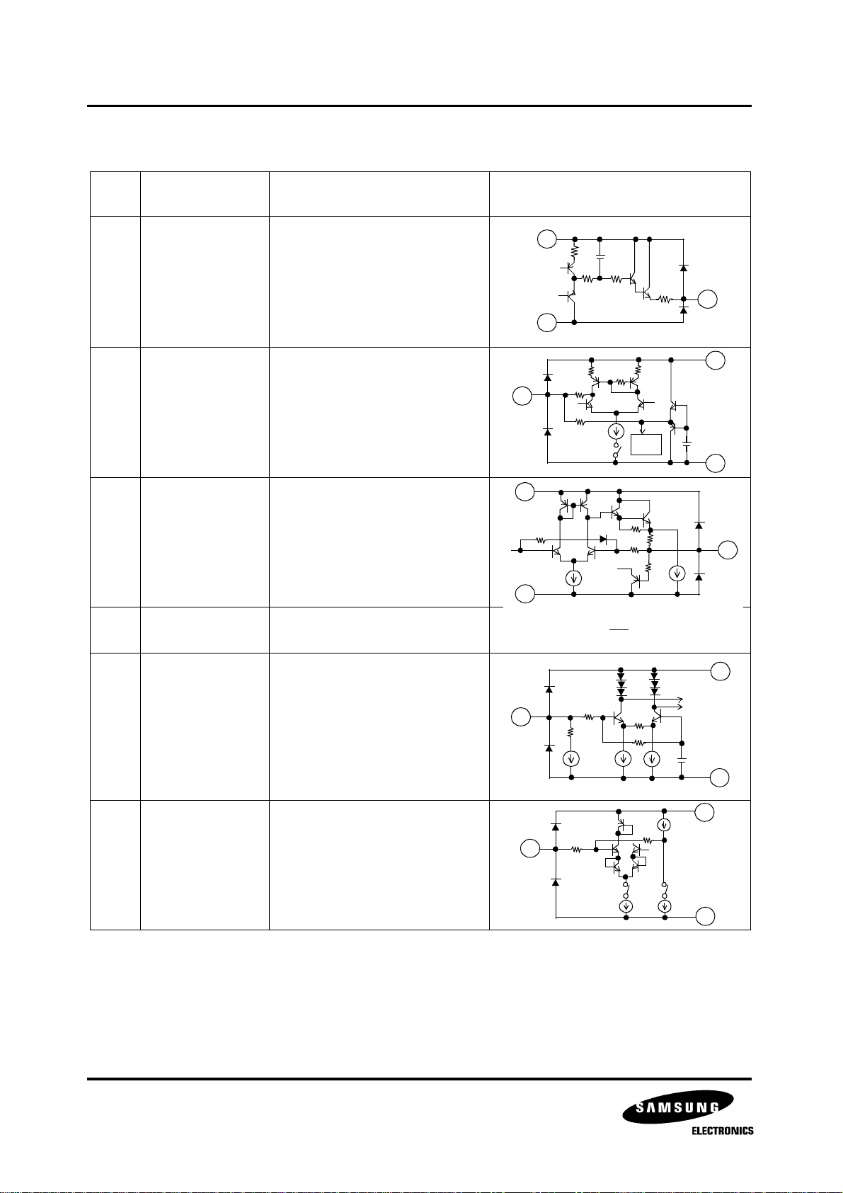
KA2163 I2C BUS NTSC 1 CHIP IC FOR COLOR TV
PIN
PIN NAME FUNCTION INTERFACE CIRCUIT
NO.
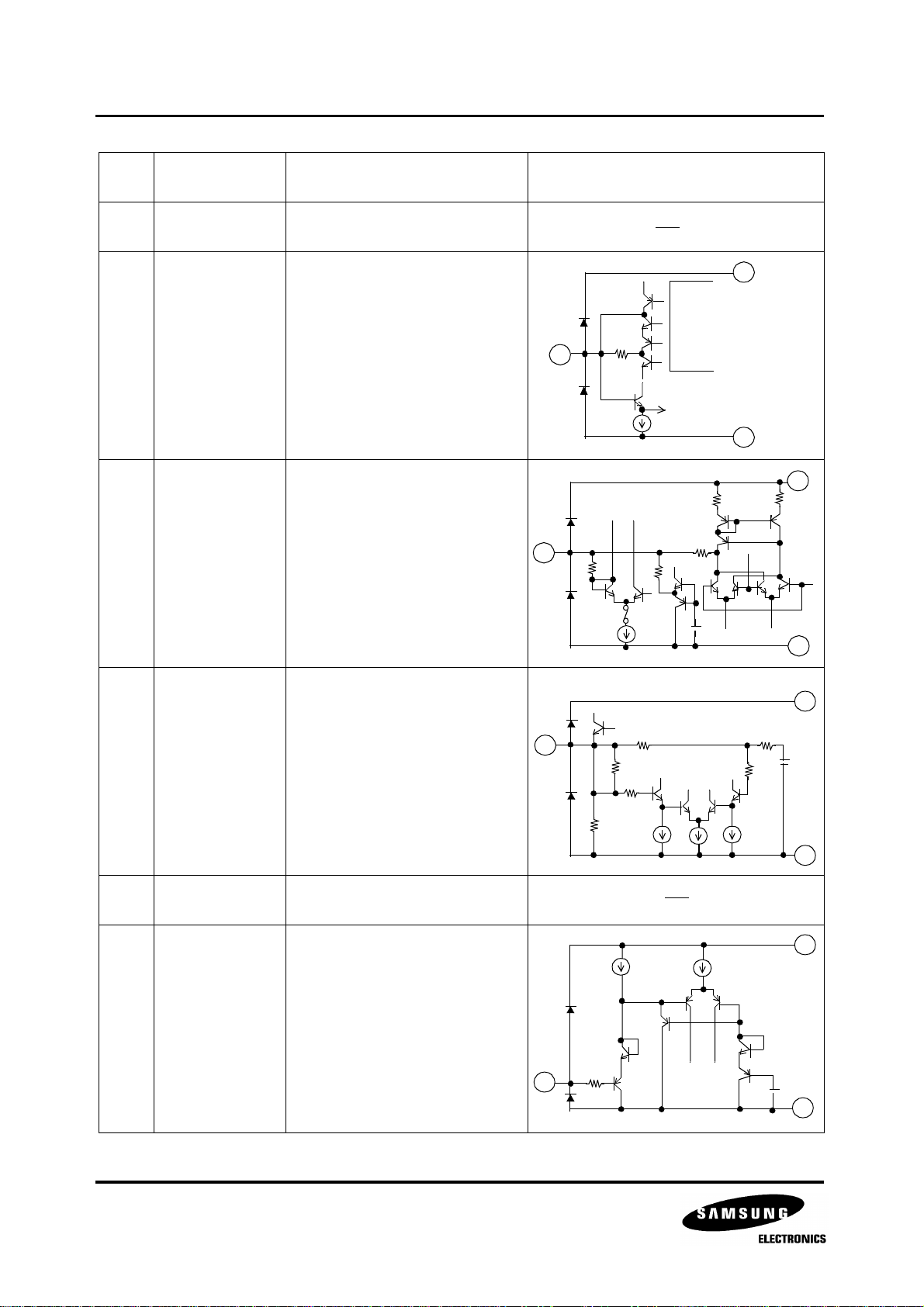
25 Vertical Sync.
Separation
This terminal is for vertical
sync. separation filter.
Filter
26 H. Vcc This terminal is for Vcc of
horizontal circuit
2728SCL, SDA These terminals are for input
and output of I2C Bus.
This terminal is for input of
X-RAY protect signal.The
threshold voltage is 3.5V
29 X-RAY
(Typ.). If applied voltage is
more than threshold voltage,
the X-RAY protect circuit will
make horizontal output a low.
27
28
25
400¥Ø
SCA 1K¥Ø
SDA 100¥Ø
29
100¥Ø
5k¥
SDA
Only
5k¥Ø
1k¥
50¥ìA
12.5¥ìA
5k¥Ø
100¥ìA
50¥ìA
3k¥Ø
150¥ìA
5k¥Ø
3.5V
13
26
13
46
3.25V
35
30 Fly-back Pulse
Input
31 Sync. Pulse
Output
6
This terminal is for Fly-back
pulse input.
The Fly-back pulse is the
reference of AFC circuit, gate
pulse and so on.
The current needs to keep
under 1mA.
This terminal is for Sync. pulse
output.
M/M-97-D008
97-05-20
30
200¥Ø
26
13
152k¥
30k¥Ø
1k¥Ø
26
HV
1.4V
13
31
KA2163 I2C BUS NTSC 1 CHIP IC FOR COLOR TV
PIN
PIN NAME FUNCTION INTERFACE CIRCUIT
NO.
32 Horizontal Output This terminal is for horizontal
pulse output.
This terminal is for horizontal
AFC filter.
33 H. AFC
The AFC circuit fits the phase
between inputed horizontal
sync. signal and horizontal
pulse which is made by
countdown 32fH.
This terminal is for connecting
ceramic oscillator. That
34 32fH VCO
constitutes 32fH (503kHz)
oscillation circuit. The
CSB503F30 (Murata) is
recommended.
33
26
13
26
13
1k¥Ø
15¥ìA
1k¥Ø
Sync.
2pF
1k¥Ø
10k¥Ø
1k¥Ø
10k¥Ø
H C.D
Input
32fH
VCO
50¥Ø
3k¥Ø
600¥ìA
32
26
13
34
35 D. GND This terminal is for GND of
digital circuit.
36 A.B.L This terminal is for A.B.L
circuit.
This terminal is for input of
37 TV Input
PIF detected signal. The typical
input amplitude is 1.0Vp-p.
36
37
1k¥Ø
1k¥Ø
100¥ìA
100¥ìA
46
10k¥Ø
10k¥
100¥ìA
3.4V
13
46
13
7
M/M-97-D008
97-05-20
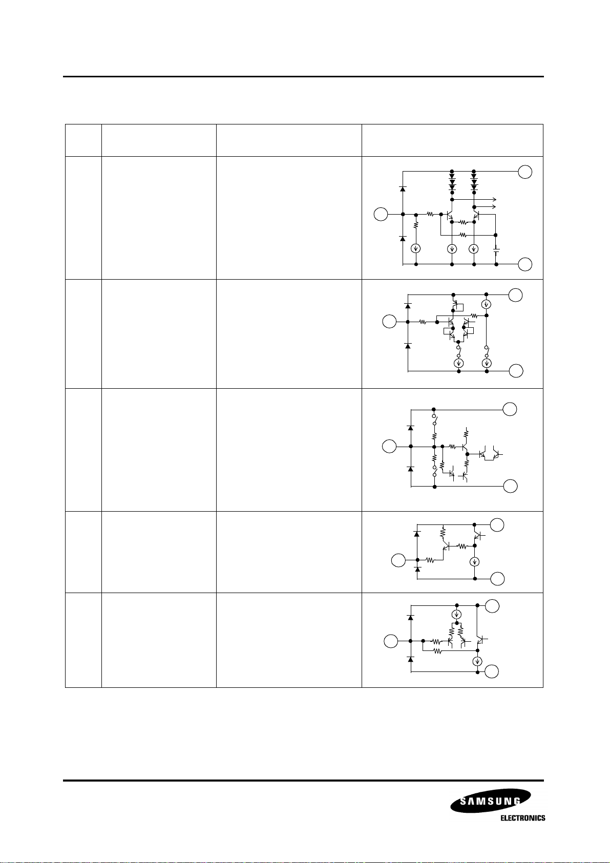
KA2163 I2C BUS NTSC 1 CHIP IC FOR COLOR TV
PIN
PIN NAME FUNCTION INTERFACE CIRCUIT
NO.
38 A.C.L This terminal is for ACL
circuit
39 External Video Input This terminal is for input of
external video signal.
38
39
1k¥Ø
1k¥Ø
100¥ìA
10k¥Ø
10k¥Ø
100¥ìA
100¥ìA
46
46
3.4V
13
46
13
40 Black Peak Detection This terminal is for filter of
black peak detection.
This terminal is for output of
41 Video Switch Output
video switch which selects
TV signal or external video.
Amplifier Gain is (Min.) 1.7
(Typ.) 1.9, (Max.) 2.1 .
42 D.C. Restoration This terminal is for filter of
APL detection.
40
42
41
3.3k¥Ø
8k¥Ø
100¥Ø
50¥
2k¥Ø
3k¥Ø
1k¥Ø
1k¥Ø
2.5k¥Ø
1.8k¥Ø
2.8k¥Ø
13
46
200¥
75¥ìA
13
46
2.5k¥
13
8
M/M-97-D008
97-05-20
KA2163 I2C BUS NTSC 1 CHIP IC FOR COLOR TV
PIN
NO.
43 Y Input
44 A.F.T.
PIN NAME FUNCTION INTERFACE CIRCUIT
3k¥Ø
This terminal is for Y signal
input.
The typical input amplitude is
1.0Vp-p.
43
1.5k¥Ø
1.5k¥Ø
150¥ìA
150¥ìA
This terminal is for AFT
output.
1k¥Ø
100¥Ø
2k¥Ø
5k¥Ø
1k¥Ø
200¥Ø
2k¥Ø
Monitor signal output mode
can be selected via Bus.
B0 B1 OUTPUT
0 0 AFT
0 1 TEST purpose only
1 0 B
1 1 RF AGC/2
180k¥Ø
44
70k¥Ø
3k¥Ø
48
RFAGC/2
X1
4.1V
51
46
13
B
This terminal is for
chrominance signal input.
The typical input signal
45 Chroma lnput
amplitude is 286mVp-p (at
burst signal).
This IC is to go to test mode
with this terminal voltage
higher than 4.5V.
This terminal is for Vcc of
46 V / C / D Vcc
video, Chroma and Deflection circuit.
47 TV Detection Output This terminal is for PIF
detected signal output.
48 S.I.F. Vcc This terminal is for Vcc of SIF
circuit.
45
47
120k¥Ø
1k¥Ø
120k¥Ø
20k¥Ø
40pF
30k¥Ø
200k¥Ø
1k¥Ø
500¥ìA
Killer
15k¥Ø
2k¥Ø
2pF
46
30k¥Ø
13
48
40k¥Ø
51
9
M/M-97-D008
97-05-20
KA2163 I2C BUS NTSC 1 CHIP IC FOR COLOR TV
PIN
PIN NAME FUNCTION INTERFACE CIRCUIT
NO.
These terminals are for
connecting a tank coil of PIF
4950P.I.F. Tank Coil
detection circuit.
TOKO Corp. products
292GJAS-7475BS(45.75MHz),
292GJAS-7476BS (58.75MHz)
are recommended.
51 S.I.F. GND This terminal is for GND of SIF
circuit.
52 Limiter lnput This terminal is for input of
SIF limiter amplifier circuit.
This terminal is for input of
53 TV Audio Signal
Input
SIF detected signal.
This terminal is connected to
pin 54 via capacitor.
49
50
53
52
600¥
30k¥
600¥
10pF
20k¥Ø
200¥
3V
3V
600¥
1k¥
1k¥
4.5k¥
23k¥Ø
Audio Switch
50¥ìA
2k¥Ø
48
200¥ìA
51
48
51
48
500¥
500¥
2k¥Ø
51
54 De-emphasis This terminal for filter of
SIF de-emphasis.
5556External Audio
Input
10
These terminals are for
external audio input.
M/M-97-D008
97-05-20
55
53
23.5k¥
23.5k¥
3V
200¥
30k¥
4.5V
10pF
48
Audio Switch
50¥ìA
48
51
51
KA2163 I2C BUS NTSC 1 CHIP IC FOR COLOR TV
Slave address : 88H
SUB
ADDRESS
00 Trap Color 0000 0000
01 C.Filter Tint 1100 0000
02 A. SW Brightnes 0000 0000
03 BLK Uni-color 0000 0000
04 Mute Sharpness 0110 0000
05 Vertical Phase Horizontal Phase 0001 0000
06 B0 B1 Audio Attenuator 0000 0000
07 B2 B3 DON’T USE (Fix on 100000) 0010 0000
08 B4 V. SW RF AGC 0000 0000
09 AFC WPL Vertical Amplitude 0010 0000
0A V.Fixed PIF VCO 0100 0000
0B R Cut OFF 0000 0000
0C G Cut OFF 0000 0000
0D B Cut Off 0000 0000
0E R Gain 0000 0000
0F B Gain 0000 0000
D7 D6 D5 D4 D3 D2 D1 D0 PRESET
FUNCTION RANGE (MIN. ~ MAX.) DEFAULT
Color -60 ~ 0dB -60dB
TINT ¡¾42¡£ 0¡£
Brightness 1.34 ~ 2.6 ~ 3.86V 1.34V
Uni-Color -24 ~ 0dB -24dB
Sharpness -18 ~ 6dB ~ 14dB (4MHz Gain) 6dB
Audio ATT -85 ~ 6dB -85dB
RF AGC 65dB¥ì ~ 105d¥ìV (0.6dB / bit), 000000 : IF Mute IF Mute
Ver. Amplitude 1.6 ~ 2.4V Center
PIF VCO ¡¾2.2MHz (35kHz / bit) Center
RGB Cut-off -0.4 ~ 0.4V -0.4V
RB Gain -3.1 ~ 3.1dB -3.1dB
11
M/M-97-D008
97-05-20
KA2163 I2C BUS NTSC 1 CHIP IC FOR COLOR TV
FUNCTION RANGE (MIN. ~ MAX.) DEFAULT
3.58 Trap ( 0 ) : On / ( 1 ) : Off On
Chroma Filter ( 0 ) : Band Pass Filter / (1) : Take Off Filter TOF
A, V SW ( 0 ) : TV Mode / (1) : EXT. Mode TV
BLK ( 0 ) : BLK On / (1) : BLK Off On
MUTE (00) : Off / (01) : Y MUTE / (10) : Hout Stop / (11) : Y MUTE + V Stop (01)
H. AFC ( 0 ) : AFC2 Normal / (1) : AFC2 x 3 ( 0 )
WPL ( 0 ) : On / (1) : Off Off
V. Fixed Mode ( 0 ) : Normal / (1) : V Frequency 60Hz Fix Normal
Pin 44’s output is selectable.
B0, B1 (Monitor)
(00) : AFT Voltage / (01) : Test Mode / (10) : Blue Output /
(11) : Half of RF AGC Voltage
AFT
Voltage
B2, B3, B4
(Test Mode)
Bits for Test Mode.
Use this IC with these bits (000). (000)
Read Mode
D7 D6 D5 D4 D3 D2 D1 D0
POR AFT IF Lock AFT - V Lock H Lock X-RAY
FUNCTION CONTENTS
POR (Power On Reset) ( 0 ) : SECOND / ( 1 ) : FIRST
AFT Refer to Following Figure
IF LOCK ( 0 ) : LOCK OUT / ( 1 ) : LOCK IN
V LOCK ( 0 ) : LOCK IN / ( 1 ) : LOCK OUT Det. Window : 262H ~ 263H
H LOCK ( 0 ) : LOCK OUT / ( 1 ) : LOCK IN This function is forced to unlock at Vp, so
data is valid after 50H.
X-RAY ( 0 ) : X-RAY OFF / ( 1 ) : X-RAY ON
¡Û Vertical Phase (3bit)
This mode is for changing vertical output timing.
(Vertical picture position is changed 0 ~ 7H as right Table.)
¡Û Horizontal Phase (5bit)
This mode is for changing horizontal picture position.
Horizontal output phase is changed ¡¾3¥ìs as maximum.
D7 D6 D5 MODE
0 0 0 Reference
0 0 1 1H Delay
0 1 0 2H Delay
¡Û AFT Read Bus
0 1 1 3H Delay
12
3.3V
1.7V
D6
D4
AFT
1 0 0 4H Delay
1 0 1 5H Delay
1 1 0 6H Delay
1 1 1 7H Delay
M/M-97-D008
97-05-20
KA2163 I2C BUS NTSC 1 CHIP IC FOR COLOR TV
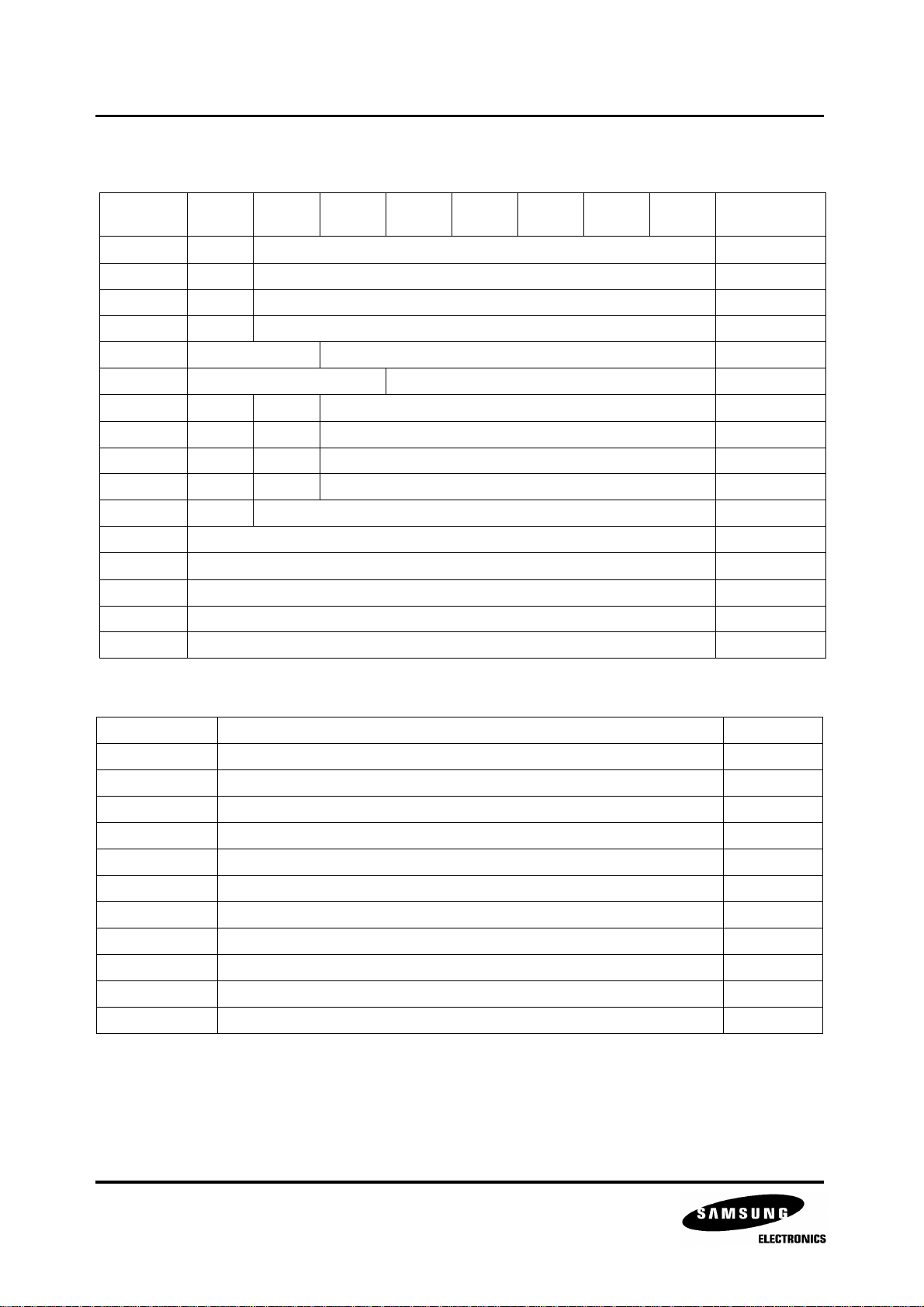
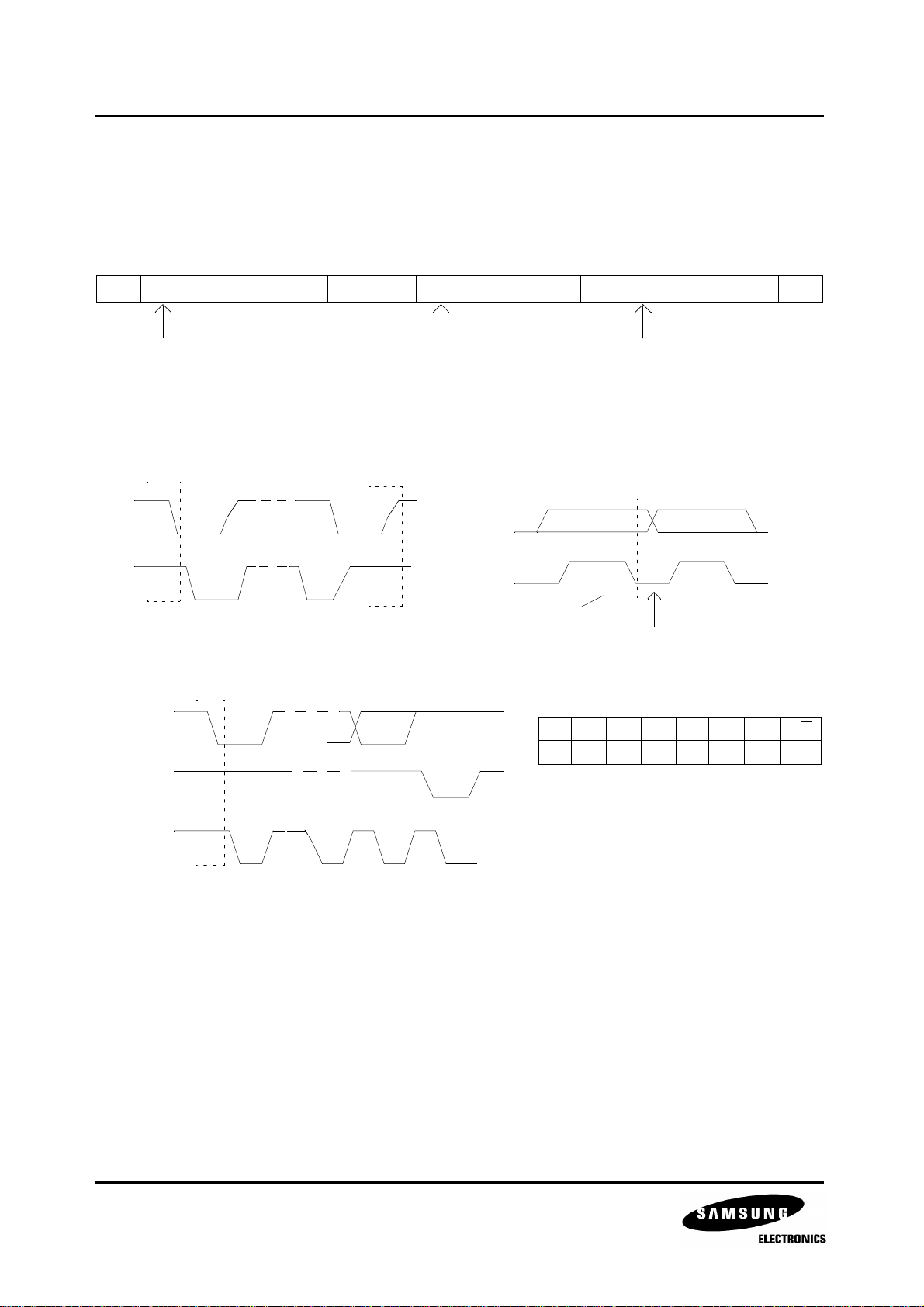
I2C BUS CONTROLLED FORMAT SUMMARY
Bus controlled format of KA2163B is based on I2C Bus Control format of Philips.
Data Transfer Format
S Slave address 0 A Sub address A Data A P
7 bit
8 bit
MSB MSB
S : Start Condition
P : Stop Condition
A : Acknowledge
(1) Start and Stop Condition (2) Bit Transfer
SDA
SDA
8 bit
SCL
S
Start Condition
P
Stop Condition
SCL
SDA cannot change.
SDA can change.
(3) Acknowledge
(4) Slave Address
SDA
from Slave
SDA
High lmpedance
High lmpedancefrom Master
A6 A5 A4 A3 A2 A1 A0 R/W
1 0 0 0 1 0 0 0
from Master
SCL
Purchase of SAMSUNG I2C components conveys a license under the Philips Iicense under the Philips I2C Patent
Rights to use these components in an I
S
1
8
2
C system, provided that the system conforms to the I2C Standard
9
Specification as defined by Philips.
13
M/M-97-D008
97-05-20
 Loading...